EP1841206A2 - Responsivity correction for electro-optical imagers - Google Patents
Responsivity correction for electro-optical imagers Download PDFInfo
- Publication number
- EP1841206A2 EP1841206A2 EP07251128A EP07251128A EP1841206A2 EP 1841206 A2 EP1841206 A2 EP 1841206A2 EP 07251128 A EP07251128 A EP 07251128A EP 07251128 A EP07251128 A EP 07251128A EP 1841206 A2 EP1841206 A2 EP 1841206A2
- Authority
- EP
- European Patent Office
- Prior art keywords
- arrangement
- correction
- performance
- coefficients
- optical
- Prior art date
- Legal status (The legal status is an assumption and is not a legal conclusion. Google has not performed a legal analysis and makes no representation as to the accuracy of the status listed.)
- Ceased
Links
- 238000012937 correction Methods 0.000 title claims abstract description 29
- 230000003287 optical effect Effects 0.000 claims abstract description 16
- 230000004044 response Effects 0.000 claims abstract description 11
- 230000000694 effects Effects 0.000 claims abstract description 8
- 238000003384 imaging method Methods 0.000 claims abstract description 7
- 230000007547 defect Effects 0.000 claims abstract description 6
- 238000000034 method Methods 0.000 abstract description 5
- 238000010586 diagram Methods 0.000 description 6
- 238000012935 Averaging Methods 0.000 description 3
- 238000012986 modification Methods 0.000 description 3
- 230000004048 modification Effects 0.000 description 3
- 238000013459 approach Methods 0.000 description 2
- 230000006870 function Effects 0.000 description 1
- 238000012545 processing Methods 0.000 description 1
- 230000003595 spectral effect Effects 0.000 description 1
- 238000001228 spectrum Methods 0.000 description 1
Images



Classifications
-
- H—ELECTRICITY
- H04—ELECTRIC COMMUNICATION TECHNIQUE
- H04N—PICTORIAL COMMUNICATION, e.g. TELEVISION
- H04N23/00—Cameras or camera modules comprising electronic image sensors; Control thereof
- H04N23/80—Camera processing pipelines; Components thereof
- H04N23/81—Camera processing pipelines; Components thereof for suppressing or minimising disturbance in the image signal generation
-
- H—ELECTRICITY
- H04—ELECTRIC COMMUNICATION TECHNIQUE
- H04N—PICTORIAL COMMUNICATION, e.g. TELEVISION
- H04N25/00—Circuitry of solid-state image sensors [SSIS]; Control thereof
- H04N25/60—Noise processing, e.g. detecting, correcting, reducing or removing noise
- H04N25/61—Noise processing, e.g. detecting, correcting, reducing or removing noise the noise originating only from the lens unit, e.g. flare, shading, vignetting or "cos4"
Definitions
- the present invention relates to imaging systems. More specifically, the present invention relates to systems and methods for nonuniformity correction for imaging systems.
- Imagers in various spectral bands are used in a variety of applications, both commercial and military.
- certain imagers exhibit a significant signal rolloff toward the edges of the display. This rolloff is due to a responsivity distortion in which the gain falls off (attenuation increases) as a function of spatial location (distance from center) within one or more optical components.
- the rolloff has been labeled as the "porthole" effect and degrades image presentation as well performance.
- the resulting image presentation is degraded due to the distracting center circular region of the display that appears brighter than the edges. Performance is also degraded due to the fact that sensor signal processing wastes display dynamic range on the rolled off signal output from center to edge.
- the porthole effect is due to optical distortion.
- Optical approaches to the correction of such optical distortion have been somewhat expensive to implement.
- the optical approaches do not allow for an inexpensive retrofit of existing systems in the field.
- the inventive system includes an arrangement for sensing the performance of an optical system and providing data in response thereto and electronically correcting nonuniformity in the performance of the optical system in response thereto.
- the nonuniformity is a porthole effect.
- the arrangement for correcting includes an arrangement for providing an inverse distortion to an output of the system electronically.
- the inverse distortion is applied by generating a plurality of spatial correction coefficients from the performance data, storing the coefficients and applying the coefficients to current data from the optical system.
- the spatial correction coefficients are statistically generated gain and level correction defect maps.
- the present teachings should enable a correction of optical distortion in nonideal electro-optical systems without requiring additional optics.
- Fig. 1 is a block diagram of an imaging system in accordance with an illustrative embodiment of the present teachings.
- the system 10 includes an image sensor 12.
- the image sensor 12 may be a camera, forward looking infrared (FLIR), or other image sensor with associated optical elements therefor.
- the image sensor 12 senses energy in the spectrum of interest and feeds sensed image data to an averaging filter 14.
- the averaged sensed data is fed from the averaging filter 14 to a correction coefficient generator 16.
- the averaging filter and correction coefficient generator are implemented in software on a general-purpose computer 18.
- the correction coefficients are generated manually using MATLAB software licensed by Mathworks.
- the correction coefficients are generated by manually fitting spatially oriented gain responsivity or attenuation performance data from the sensor 12 to an optimum or desired performance curve.
- the resulting adjustments are the correction coefficients embodied in a statistically generated gain and level correction defect map required to adjust the output of the image sensor to correct for a spatially oriented nonuniformity such as the porthole effect mentioned above.
- the correction coefficients are stored in a memory 20 and selectively retrieved by a timing and control circuit 22 via a first in first out (FIFO) memory 24.
- the timing and control circuit may be implemented with a microprocessor.
- the timing and control circuit 22 serves to access the correction coefficient associated with the current data output by the image sensor on a pixel-by-pixel basis. This is illustrated in Fig. 2.
- Fig. 2(a) is a diagram of an illustrative image showing the porthole effect.
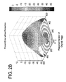
- Fig. 2(b) is a diagram showing the response variation of the original image of Fig. 2(a).
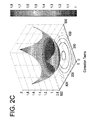
- Fig. 2(c) is a graph of a statistically generated gain and level correction defect map in accordance with the present teachings to correct the response variation of Fig. 2(b).
- Fig. 2(d) is a graph showing the response variation of the corrected image resulting the application of the correction terms of Fig. 2(c) to the original image of Fig. 2(a).
- Fig. 2(e) is a corrected image resulting from the application of the corrected terms of Fig. 2(c) to the image data of Figs. 2(a) and (b).
- the spatially oriented correction coefficients are applied through the FIFO 24 to current image data from the image sensor 12 via a multiplier 26.
- the corrected image data is forwarded to a display 30 via an optional image processor 28.
Landscapes
- Engineering & Computer Science (AREA)
- Multimedia (AREA)
- Signal Processing (AREA)
- Studio Devices (AREA)
- Photometry And Measurement Of Optical Pulse Characteristics (AREA)
- Image Processing (AREA)
- Image Input (AREA)
- Transforming Light Signals Into Electric Signals (AREA)
Abstract
Description
- The present invention relates to imaging systems. More specifically, the present invention relates to systems and methods for nonuniformity correction for imaging systems.
- Imagers in various spectral bands are used in a variety of applications, both commercial and military. Unfortunately, certain imagers exhibit a significant signal rolloff toward the edges of the display. This rolloff is due to a responsivity distortion in which the gain falls off (attenuation increases) as a function of spatial location (distance from center) within one or more optical components. The rolloff has been labeled as the "porthole" effect and degrades image presentation as well performance. The resulting image presentation is degraded due to the distracting center circular region of the display that appears brighter than the edges. Performance is also degraded due to the fact that sensor signal processing wastes display dynamic range on the rolled off signal output from center to edge.
- The porthole effect is due to optical distortion. Optical approaches to the correction of such optical distortion have been somewhat expensive to implement. In addition, the optical approaches do not allow for an inexpensive retrofit of existing systems in the field.
- Hence, a need exists in the art for an electronic system or method for improving the performance of imagers. Specifically, a need exists in the art for an electronic system or method for improving the responsivity distortion of imagers.
- The need in the art is addressed by the imaging system and method of the present invention. The inventive system includes an arrangement for sensing the performance of an optical system and providing data in response thereto and electronically correcting nonuniformity in the performance of the optical system in response thereto.
- In the illustrative application, the nonuniformity is a porthole effect. In the preferred embodiment, the arrangement for correcting includes an arrangement for providing an inverse distortion to an output of the system electronically. The inverse distortion is applied by generating a plurality of spatial correction coefficients from the performance data, storing the coefficients and applying the coefficients to current data from the optical system. The spatial correction coefficients are statistically generated gain and level correction defect maps.
- The present teachings should enable a correction of optical distortion in nonideal electro-optical systems without requiring additional optics.
-
- Fig. 1 is a block diagram of an imaging system in accordance with an illustrative embodiment of the present teachings.
- Fig. 2(a) is a diagram of an illustrative image showing the porthole effect.
- Fig. 2(b) is a diagram showing the response variation of the original image of Fig. 2(a).
- Fig. 2(c) is a graph of a defect map of correction terms generated in accordance with the present teachings to correct the response variation of Fig. 2(b).
- Fig. 2(d) is a graph showing the response variation of the corrected image resulting from the application of the correction terms of Fig. 2(c) to the original image of Fig. 2(a).
- Fig. 2(e) is a corrected image resulting from the application of the corrected terms of Fig. 2(c) to the image data of Figs. 2(a) and (b).
- Illustrative embodiments and exemplary applications will now be described with reference to the accompanying drawings to disclose the advantageous teachings of the present invention.
- While the present invention is described herein with reference to illustrative embodiments for particular applications, it should be understood that the invention is not limited thereto. Those having ordinary skill in the art and access to the teachings provided herein will recognize additional modifications, applications, and embodiments within the scope thereof and additional fields in which the present invention would be of significant utility.
- Fig. 1 is a block diagram of an imaging system in accordance with an illustrative embodiment of the present teachings. As shown in Fig. 1, the
system 10 includes animage sensor 12. Theimage sensor 12 may be a camera, forward looking infrared (FLIR), or other image sensor with associated optical elements therefor. Theimage sensor 12 senses energy in the spectrum of interest and feeds sensed image data to anaveraging filter 14. The averaged sensed data is fed from the averagingfilter 14 to acorrection coefficient generator 16. In the illustrative embodiment, the averaging filter and correction coefficient generator are implemented in software on a general-purpose computer 18. - In the preferred embodiment, the correction coefficients are generated manually using MATLAB software licensed by Mathworks. In the illustrative embodiment, the correction coefficients are generated by manually fitting spatially oriented gain responsivity or attenuation performance data from the
sensor 12 to an optimum or desired performance curve. The resulting adjustments are the correction coefficients embodied in a statistically generated gain and level correction defect map required to adjust the output of the image sensor to correct for a spatially oriented nonuniformity such as the porthole effect mentioned above. - Those skilled in the art will appreciate that the present teachings may be used to correct for other nonuniformities or to optimize the performance of the sensor in another desired manner without departing from the scope of the present teachings.
- The correction coefficients are stored in a
memory 20 and selectively retrieved by a timing andcontrol circuit 22 via a first in first out (FIFO)memory 24. The timing and control circuit may be implemented with a microprocessor. The timing andcontrol circuit 22 serves to access the correction coefficient associated with the current data output by the image sensor on a pixel-by-pixel basis. This is illustrated in Fig. 2. - Fig. 2(a) is a diagram of an illustrative image showing the porthole effect. Fig. 2(b) is a diagram showing the response variation of the original image of Fig. 2(a). Fig. 2(c) is a graph of a statistically generated gain and level correction defect map in accordance with the present teachings to correct the response variation of Fig. 2(b). Fig. 2(d) is a graph showing the response variation of the corrected image resulting the application of the correction terms of Fig. 2(c) to the original image of Fig. 2(a). Fig. 2(e) is a corrected image resulting from the application of the corrected terms of Fig. 2(c) to the image data of Figs. 2(a) and (b).
- As shown in Fig. 1, the spatially oriented correction coefficients are applied through the
FIFO 24 to current image data from theimage sensor 12 via amultiplier 26. The corrected image data is forwarded to adisplay 30 via anoptional image processor 28. - Thus, the present invention has been described herein with reference to a particular embodiment for a particular application. Those having ordinary skill in the art and access to the present teachings will recognize additional modifications applications and embodiments within the scope thereof.
- It is therefore intended by the appended claims to cover any and all such applications, modifications and embodiments within the scope of the present invention.
- Accordingly,
Claims (7)
- An imaging system (10) characterized by:an image sensor (12) for sensing the performance of an optical system and providing data in response thereto andan arrangement (18, 26) responsive to said data for electronically correcting nonuniformity in said performance of said optical system.
- The invention of Claim 1 wherein said nonuniformity is a porthole effect.
- The invention of Claim 1 wherein said arrangement for correcting includes an arrangement (18) for providing an inverse distortion to an output of said system electronically.
- The invention of Claim 3 wherein said arrangement for providing an inverse distortion includes an arrangement (16) for generating a plurality of spatial correction coefficients.
- The invention of Claim 4 wherein said system (10) includes memory (20) for storing said correction coefficients.
- The invention of Claim 5 wherein said system (10) includes a multiplier (26) for applying said correction coefficients to image data.
- The invention of Claim 6 wherein said spatial correction coefficients provide statistically generated gain and level correction defect maps.
Applications Claiming Priority (1)
| Application Number | Priority Date | Filing Date | Title |
|---|---|---|---|
| US11/393,989 US7683945B2 (en) | 2006-03-30 | 2006-03-30 | Responsivity correction for electro-optical imagers |
Publications (2)
| Publication Number | Publication Date |
|---|---|
| EP1841206A2 true EP1841206A2 (en) | 2007-10-03 |
| EP1841206A3 EP1841206A3 (en) | 2009-08-19 |
Family
ID=38222522
Family Applications (1)
| Application Number | Title | Priority Date | Filing Date |
|---|---|---|---|
| EP07251128A Ceased EP1841206A3 (en) | 2006-03-30 | 2007-03-16 | Responsivity correction for electro-optical imagers |
Country Status (2)
| Country | Link |
|---|---|
| US (1) | US7683945B2 (en) |
| EP (1) | EP1841206A3 (en) |
Citations (3)
| Publication number | Priority date | Publication date | Assignee | Title |
|---|---|---|---|---|
| EP0447187A2 (en) | 1990-03-13 | 1991-09-18 | Sony Corporation | Shading correction apparatus |
| US20040125227A1 (en) | 2002-11-13 | 2004-07-01 | Hidekazu Tsuruoka | Camera module |
| EP1447977A1 (en) | 2003-02-12 | 2004-08-18 | Dialog Semiconductor GmbH | Vignetting compensation |
Family Cites Families (7)
| Publication number | Priority date | Publication date | Assignee | Title |
|---|---|---|---|---|
| US5473426A (en) * | 1993-03-05 | 1995-12-05 | Nikon Corporation | Defect inspection apparatus |
| US5604347A (en) * | 1995-07-13 | 1997-02-18 | General Electric Company | Method and means for compensating for row variable offsets in a large area solid state x-ray detector |
| US5721427A (en) * | 1996-12-19 | 1998-02-24 | Hughes Electronics | Scene-based nonuniformity correction processor incorporating motion triggering |
| US6028309A (en) * | 1997-02-11 | 2000-02-22 | Indigo Systems Corporation | Methods and circuitry for correcting temperature-induced errors in microbolometer focal plane array |
| US6687414B1 (en) * | 1999-08-20 | 2004-02-03 | Eastman Kodak Company | Method and system for normalizing a plurality of signals having a shared component |
| US6965692B1 (en) * | 1999-12-30 | 2005-11-15 | Eastman Kodak Company | Method and apparatus for improving the quality of reconstructed information |
| US6901173B2 (en) * | 2001-04-25 | 2005-05-31 | Lockheed Martin Corporation | Scene-based non-uniformity correction for detector arrays |
-
2006
- 2006-03-30 US US11/393,989 patent/US7683945B2/en active Active
-
2007
- 2007-03-16 EP EP07251128A patent/EP1841206A3/en not_active Ceased
Patent Citations (3)
| Publication number | Priority date | Publication date | Assignee | Title |
|---|---|---|---|---|
| EP0447187A2 (en) | 1990-03-13 | 1991-09-18 | Sony Corporation | Shading correction apparatus |
| US20040125227A1 (en) | 2002-11-13 | 2004-07-01 | Hidekazu Tsuruoka | Camera module |
| EP1447977A1 (en) | 2003-02-12 | 2004-08-18 | Dialog Semiconductor GmbH | Vignetting compensation |
Non-Patent Citations (1)
| Title |
|---|
| NARENDRA P M: "Scene-based nonuniformity compensation for imaging sensors", IEEE TRANSACTIONS ON PATTERN ANALYSIS AND MACHINE INTELLIGENCE, vol. 30, no. 1, 1 January 1982 (1982-01-01) |
Also Published As
| Publication number | Publication date |
|---|---|
| US20070229681A1 (en) | 2007-10-04 |
| US7683945B2 (en) | 2010-03-23 |
| EP1841206A3 (en) | 2009-08-19 |
Similar Documents
| Publication | Publication Date | Title |
|---|---|---|
| EP3306915B1 (en) | Method and apparatus for controlling image data | |
| US8537269B2 (en) | Method, medium, and apparatus for setting exposure time | |
| US7671892B2 (en) | Image sensing apparatus, and control method, program, and storage medium of image sensing apparatus | |
| US5721427A (en) | Scene-based nonuniformity correction processor incorporating motion triggering | |
| CN106127693B (en) | Defogging system and defogging method | |
| US20090009604A1 (en) | Image processing system and method | |
| US20040218063A1 (en) | Correction apparatus | |
| US9582868B2 (en) | Image processing apparatus that appropriately performs tone correction in low-illuminance environment, image processing method therefor, and storage medium | |
| US9338366B2 (en) | Apparatus and method for compensating for back light of image | |
| JP2002027491A (en) | Image input apparatus, white balance adjustment method, and computer-readable recording medium storing program for executing the method | |
| JP6186465B2 (en) | Electronic display adjustment based on gaze tracking | |
| JP2009512303A (en) | Method and apparatus for removing vignetting in digital images | |
| JP2002323382A (en) | Apparatus for determining color temperature of ambient illumination light and method of classifying illumination light | |
| US20100245608A1 (en) | Adaptive method and system for extracting a bright image from a thermal image | |
| JP2008276482A (en) | Image processing apparatus, image processing method, and image processing program | |
| US8111308B2 (en) | Signal processing apparatus, signal processing method, and image pickup apparatus | |
| US20040047012A1 (en) | Method and device for imaging using several exposure times | |
| JP2019149764A (en) | Display device calibration device, display device calibration system, display device calibration method, and display device | |
| US20220293022A1 (en) | Display device, display control method, and non-transitory computer-readable recording medium | |
| EP1293092B1 (en) | Infrared detection system and method with histogram based manual level and gain control | |
| US7683945B2 (en) | Responsivity correction for electro-optical imagers | |
| US20030122938A1 (en) | Resolution correction apparatus, resolution correction program, and computer-readable recording medium having same program recorded thereon | |
| US8427542B2 (en) | Image calibration method and image processing system utilizing the method | |
| KR20100114343A (en) | Apparatus for correcting channel sensitivity and lens shading of a photographed image and method thereof | |
| US20170053386A1 (en) | Image processing apparatus and image processing method |
Legal Events
| Date | Code | Title | Description |
|---|---|---|---|
| PUAI | Public reference made under article 153(3) epc to a published international application that has entered the european phase |
Free format text: ORIGINAL CODE: 0009012 |
|
| AK | Designated contracting states |
Kind code of ref document: A2 Designated state(s): AT BE BG CH CY CZ DE DK EE ES FI FR GB GR HU IE IS IT LI LT LU LV MC MT NL PL PT RO SE SI SK TR |
|
| AX | Request for extension of the european patent |
Extension state: AL BA HR MK YU |
|
| PUAL | Search report despatched |
Free format text: ORIGINAL CODE: 0009013 |
|
| AK | Designated contracting states |
Kind code of ref document: A3 Designated state(s): AT BE BG CH CY CZ DE DK EE ES FI FR GB GR HU IE IS IT LI LT LU LV MC MT NL PL PT RO SE SI SK TR |
|
| AX | Request for extension of the european patent |
Extension state: AL BA HR MK RS |
|
| 17P | Request for examination filed |
Effective date: 20100104 |
|
| AKX | Designation fees paid |
Designated state(s): DE FR GB |
|
| 17Q | First examination report despatched |
Effective date: 20111125 |
|
| STAA | Information on the status of an ep patent application or granted ep patent |
Free format text: STATUS: THE APPLICATION HAS BEEN REFUSED |
|
| 18R | Application refused |
Effective date: 20120914 |