EP1841058A1 - Method and system to improve local oscillator signal rejection in single-sideband radiofrequency up-converters - Google Patents
Method and system to improve local oscillator signal rejection in single-sideband radiofrequency up-converters Download PDFInfo
- Publication number
- EP1841058A1 EP1841058A1 EP06425224A EP06425224A EP1841058A1 EP 1841058 A1 EP1841058 A1 EP 1841058A1 EP 06425224 A EP06425224 A EP 06425224A EP 06425224 A EP06425224 A EP 06425224A EP 1841058 A1 EP1841058 A1 EP 1841058A1
- Authority
- EP
- European Patent Office
- Prior art keywords
- power
- mixer
- residual
- signal
- converter
- Prior art date
- Legal status (The legal status is an assumption and is not a legal conclusion. Google has not performed a legal analysis and makes no representation as to the accuracy of the status listed.)
- Granted
Links
- 238000000034 method Methods 0.000 title claims description 25
- 230000000694 effects Effects 0.000 claims abstract description 9
- 238000010009 beating Methods 0.000 claims abstract description 7
- 230000006870 function Effects 0.000 claims description 15
- 238000001514 detection method Methods 0.000 claims description 5
- 238000006243 chemical reaction Methods 0.000 claims description 4
- 230000008859 change Effects 0.000 abstract description 3
- 230000001629 suppression Effects 0.000 description 8
- 230000032683 aging Effects 0.000 description 5
- 101100521334 Mus musculus Prom1 gene Proteins 0.000 description 4
- 230000006399 behavior Effects 0.000 description 4
- 230000010287 polarization Effects 0.000 description 4
- 238000010586 diagram Methods 0.000 description 3
- 230000009471 action Effects 0.000 description 2
- 238000002955 isolation Methods 0.000 description 2
- 239000000243 solution Substances 0.000 description 2
- 230000003595 spectral effect Effects 0.000 description 2
- 238000001228 spectrum Methods 0.000 description 2
- 230000003068 static effect Effects 0.000 description 2
- PNEYBMLMFCGWSK-UHFFFAOYSA-N aluminium oxide Inorganic materials [O-2].[O-2].[O-2].[Al+3].[Al+3] PNEYBMLMFCGWSK-UHFFFAOYSA-N 0.000 description 1
- 230000003321 amplification Effects 0.000 description 1
- 230000005540 biological transmission Effects 0.000 description 1
- 238000004891 communication Methods 0.000 description 1
- 230000003750 conditioning effect Effects 0.000 description 1
- 230000007423 decrease Effects 0.000 description 1
- 230000003247 decreasing effect Effects 0.000 description 1
- 230000001419 dependent effect Effects 0.000 description 1
- 229920005994 diacetyl cellulose Polymers 0.000 description 1
- 238000006073 displacement reaction Methods 0.000 description 1
- 238000002347 injection Methods 0.000 description 1
- 239000007924 injection Substances 0.000 description 1
- 238000004519 manufacturing process Methods 0.000 description 1
- 238000012986 modification Methods 0.000 description 1
- 230000004048 modification Effects 0.000 description 1
- 238000003199 nucleic acid amplification method Methods 0.000 description 1
- 230000009467 reduction Effects 0.000 description 1
- 230000004044 response Effects 0.000 description 1
- 230000035945 sensitivity Effects 0.000 description 1
- 239000000758 substrate Substances 0.000 description 1
- 239000010409 thin film Substances 0.000 description 1
- 230000001052 transient effect Effects 0.000 description 1
Images



Classifications
-
- H—ELECTRICITY
- H03—ELECTRONIC CIRCUITRY
- H03C—MODULATION
- H03C1/00—Amplitude modulation
- H03C1/52—Modulators in which carrier or one sideband is wholly or partially suppressed
- H03C1/60—Modulators in which carrier or one sideband is wholly or partially suppressed with one sideband wholly or partially suppressed
Definitions
- the present invention relates to the field of radio transmitters, and more precisely to a method and system to improve local oscillator signal rejection in single-sideband radiofrequency up-converters.
- Standard RF up-converters generally include mixer diodes in balanced configuration.
- the most used techniques to improve the performance are the design of very accurate balanced mixer or the use of high Q filter at RF mixer port; anyway both these solutions can show some drawbacks such us narrow band operation, low LO suppression at high frequency and expensive circuitry.
- a good method to suppress the local oscillator signal completely is to improve the mixer symmetry by biasing each of the diodes or by applying a differential voltage for two diodes. But when the frequency is changed, the bias voltage has to be readjusted. Furthermore, by effect of temperature variations and aging the grade of balancing may change during the operational life of the mixing diodes and the LO rejection is no more optimal, consequently.
- the circuitry employs well known phasing methods to build a single-sideband frequency converter by using two identical balanced or double-balanced mixer circuits 2, 3 together with power splitter and quadrature hybrids 4 and 5.
- the balanced RF signal between the outputs of the two converters 2 and 3 applied to the two ends of an interposed resistor 6, is coupled to an output RF port 7.
- Single side-sideband does not solve the problem of poor local oscillator isolation with respect to the RF output level.
- the synthesizer 1 further outputs on two distinct buses a same digital word which is the one necessary to set the frequency of the LO.
- the two digital words are used to control two identical electronic circuits which can adjust the proper bias voltages of respective mixers 2 and 3 for every used frequency.
- These are very simple circuits consisting of a PROM 8, 8' followed by a digital-to-analog converter 9, 9' and an operational amplifier 10, 10'. If, for example, 8 bits are used, the bias voltages far up to 256 channels can be stored in a memory.
- the synthesizer frequency is set, the frequency information is given to the two PROMs 8 and 8'.
- the output of PROM 8 feeds the digital-to-analog converter 9, the analog voltage from the conversion applied at the input of the operational amplifier 10 causes a bipolar output voltage for biasing the mixer 2. The same happens on the other branch.
- Polarity and value of the bias voltage is determined by said digital word.
- the two bias voltages are used as differential bias for each of the two balanced mixers 2 and 3; each voltage can have values between +V REF and in -V REF in 256 increments, this is sufficient far all cases.
- the LO-level at the mixer output is in a first step measured and, in a second step, optimized for best suppression by adjusting the bias voltages. These voltages are evaluated for each oscillator frequency and stored in the PROM. This time-consuming procedure is simplified by the use of a computer controlled measuring system consisting of a spectrum analyzer, such as the HP 8566A, and a desktop computer. As can be directly seen on the display of HP 8566A, biasing with differential bias only affects the suppression of local oscillator; upper and suppressed lower sideband and all other higher order products remain unchanged. This can be done far every used local oscillator frequency.
- Object of the present invention is to improve the LO signal rejection without that static calibration tables are needed.
- the invention achieves the declared object by providing a method to improve local oscillator LO signal rejection in single-sideband radiofrequency up-converters comprising a balanced or double-balanced mixer biased with differential currents adjustable to improve said rejection, as disclosed in claim 1.
- the method of the invention includes the following steps:
- the function f(Id1, Id2) is either derivable by means of pure theoretical considerations or experimentally by interpolating through a grid of measures involving pairs of close bias currents Id1, Id2 and corresponding quasi-continuous voltages obtained by the LO residual power down-converted to IF.
- the function f(Id1, Id2) reflects the non-linear behaviour of the mixer, let us assume the shape of f(Id1, Id2) is the same for all production lot of up-converters but slightly differently offset in respect of the axes: well, the gradient equalizes the whole functions independently of their offsets, consequently it is calculated only once and stored locally.
- object of the invention is a system to improve local oscillator signal rejection in single-sideband radiofrequency up-converter comprising a balanced or double-balanced mixer biased with differential currents and operating according to the method of above, as disclosed in a device independent claim.
- the mixer can be implemented using diodes or FETs, indifferently, although diodes are preferable.
- the system of the invention improves the rejection of the LO signal by means of a bias calibration feedback loop for recovering possible mixer unbalances .
- the bias calibration feedback loop is set to exploit the mixing effect of an RF detector that belongs to an automatic level control loop (ALC) acting on the RF power amplifier.
- ALC automatic level control loop
- Said feedback loop originates from an RF power splitter connected to an auxiliary mixer which constitutes the RF detector driven by the output RF signal power.
- ALC automatic level control loop
- the IF power originated from down conversion of residual LO is used to derive optimal bias voltage/current values across the double-balanced mixer, so as to minimize the residual power of LO.
- Any suitable known minimization algorithm can be used. Due to the wide dynamic range of the IF power, a cheap logarithmic amplifier further operating as level detector is provided at the input of conditioning circuitry.
- the latter includes a microprocessor with ADC and DACs at the input and outputs, respectively, and two operational amplifiers configured as voltage-to-current converters which pilot the double-balanced mixer with differential currents.
- the bias calibration feedback loop is made completely independent of the ALC loop.
- a first power splitter is used to derive the RF signal power at the output of the up-converter, opportunely amplified, towards the input of the bias calibration loop.
- a second power splitter is used, with or without a relaxed interstage RF filter, to derive the RF power at the output of the final RF amplifier towards the input of the ALC loop.
- the residual power of LO down-converted to IF has low dynamic range and a simple operational amplifier instead of logarithmic is used. The steady state can be reached before switching the RF power amplifier on at power up.
- the preferred and the alternative embodiments of the invention allow wideband operation and improve LO rejection without needing a narrowband interstage RF filter.
- the first embodiment is cheaper because a mixer and a power splitter is saved, but the LO residual power converted back to IF is in minor measure affected by the indirect RTPC action on the RF detector.
- the second embodiment is more expensive but allows good and stable suppression because the LO residual power is independent from the RTPC action.
- transient lack of LO suppression like it can happen for example at power-up or when a large output power variation occurs, can generally be tolerated by the two embodiments because only output power precision is affected, while spurious emission limits are always guaranteed by a diplexer filter.
- IRM Image Rejection Mixer
- the IRM block 20 includes a double-balanced diode mixer 20' pumped by a LO sinusoidal signal generated by a local oscillator 21, a first quadrature hybrid 22a, and a second quadrature hybrid 22b.
- the first quadrature hybrid 22a operates as IF splitter connected to a balanced IF port of the double-balanced diode mixer 20'.
- the second quadrature hybrid 22b operates as RF combiner connected to a balanced RF port of mixer 20', which also receives the unbalanced LO signal injected in-phase at a LO port.
- Two analog DC polarization blocks 23 and 24 individually controlled by a Mixer Control block 25 are connected to respective biasing inputs of mixer 20'.
- the IF input signal is frequency converted by the IRM block into a single-sideband RF signal which undergoes a first amplification by a RF pre-amplifier 26.
- the latter is cascaded by an RF interstage bandpass filter 28 and a variable-gain transmission power amplifier 29.
- Bandpass filter 28 is not mandatory and when is used has relaxed out of band characteristic.
- the TX power amplifier 29 is coupled to a RF power splitter 30 which splits the RF signal towards a diplexer filter 31 and a detection and control loop including a power detector and mixer diode 40 and an ALC block connected to the gain control input of the RF power amplifier 29.
- the spurious emission limits are always guaranteed by diplexer filter 31.
- the biasing calibration feedback loop includes the cascade of the following blocks: the mixer 40, an IF bandpass filter 35, a Log-detector amplifier 41, an A/D converter 38, the Mixer Control block 25, two D/A converters 42, 43, and the biasing blocks 23, 24.
- Component 40 is a diode pumped by the RF power so as to down-convert to IF at the output of the bandpass filter 35 (the IF BACK spectral line visible in the lowest ellipse) the residual of LO (LO RES spectral line visible in the uppermost ellipse).
- the element 41 is a logarithmic amplifier operating as envelope detector of the down-converted IF power.
- a logarithmic amplifier is needed because of the large dynamic of the IF envelope due to dependence on the RTCP functionality.
- the output of the Log-detector amplifier 41 is a DC signal V REG directed to the A/D converter 38 at the input of the microcontroller 25.
- the latter calculates two digital values Vd1 and Vd2 useful to update the diode mixer polarizations and forwards them to respective D/A converters 42, 43.
- the analog Vd1, Vd2 voltages are input to DC blocks 23 and 24, respectively to be converted into biasing current Id1 and Id2, respectively.
- fig.3a An equivalent circuit of a double-balanced mixer (corresponding to the block 20' inside the IRM 20) valid for the only signals excluded polarization is visible in fig.3a; the circuit includes two pairs of serially connected diodes D1, D2 and D3, D4. The two pairs of diodes are connected in counterphase and are fed at the centre of the two diodes with unbalanced LO signal. The RF and IF ports are both balanced with respect to ground.
- Fig.3b shows the circuital realization of the DC biasing blocks 23 and 24. With reference to fig.3b, the two identical blocks 23 and 24 include an operational amplifier in voltage-to-current converter configuration with the load connected to ground.
- Block 23 includes four resistors R1, R2, R3, and R4, of which: R3 and R4 are connected between the output Vo and the inputs + and -, respectively; R2 is connected between the input + and ground; R1 is connected to the output of D/A 43 and the input - of the operational in order to input the biasing voltage Vd1.
- a biasing voltage Vp1 Id1xZd1 is set across the load Zd1.
- Fig.5 shows an alternative embodiment of the circuitry for the suppression of residual LO, where the same elements as in fig.2 are indicated by the same symbols.
- a splitter 27 splits the RF signal at the output of the pre-amplifier 26 into two signals and forwards a first one to an ALC control part and a second one to a feedback biasing calibration loop.
- the ALC loop is separated from the splitter 27 by an RF interstage bandpass filter 28 that is not mandatory and, if present, has relaxed out of band characteristic.
- the ALC loop includes a variable gain RF power amplifier 29 coupled to a power splitter 30 which splits the RF signal towards a diplexer filter 31 and a detection and control loop including a power detector diode 32 and an ALC block connected to the gain control input of the RX power amplifier 29.
- the spurious emission limits are always guaranteed by diplexer filter 31.
- the biasing calibration feedback loop includes the cascade of the following blocks: a mixer 34 pumped by the RF signal, an IF bandpass filter 35, an IF amplifier 36, an IF detector 37, and blocks 38, 25, 42, 43, 23 and 24.
- a mixer 34 pumped by the RF signal
- an IF bandpass filter 35 an IF amplifier 36
- an IF detector 37 at the output of mixer 34 an IF BACK intermediate frequency power which follows the residual power of LO is obtained.
- This IF BACK power is originated from the beating between residual LO from the system IF up-conversion and the RF signal as driving power.
- the output of the IF detector 37 is a DC signal V REG directed to the A/D converter 38 at the input of the microcontroller 25.
- the latter calculates two digital values Vd1 and Vd2 for updating two bias voltages of block IRM 20, separately, and forwards them to the respective D/A converters 42, 43.
- the DC bias voltages of mixer diodes are separately adjusted.
- an experimental 38 GHz up-converter supporting 128 QAM modulated signal is used.
- the IF input signal is -5 dBm at 350 MHz
- the LO signal is +15 dBm at 38.35 GHz
- the RF converted signal is 15 dBm at 38 GHz (Lower Side Band)
- the LO signal leakage at output LO res is -15 dBm at 38 GHz, that is 30 dBc below the usefull RF signal.
- Our goal is to obtain 50 dBc below.
- the biasing calibration method is nearly the same for the two embodiments of the invention, so that the only one of fig.2 is discussed.
- the ALC detector 40 acts as a down-converter mixer too, anyway in this case the pump signal is the RF signal and the ORES is the input signal.
- the downconverted signal is the regenerated IF signal IF BACK at 350 MHz with a power level of -50 dBm. This signal is linear related to the LO RES signal; if LO RES 1 dB decreases, IF BACK 1 dB dcreases too.
- the log-detector 41 which is fed by the IF BACK signal, generates a DC signal V REG that is used by the microcontroller 25 to adjust the biasing of mixer diodes to improve LO signal output suppression.
- the log-detector is used in order to have a wide dynamic range and a high detection sensitivity.
- the microcontroller routine works according the following steps shown in fig.6.
- the microcontroller 25 in standby status S1 is switched on in step S2 to start the LO RES minimization routine based on the well known gradient method or one of its many variants, e.g.: steepest descent, conjugate gradient, etc.
- the aim of the method is to find a local minimum of a function f( x ) iteratively, starting from an initial point x 0 and terminating only when the absolute gradient value falls below an ⁇ value as small as whished.
- the argument of the object function f( x ) is a n-dimensional vector x.
- the function V REG (Id1, Id2) is achievable in known way from the following items:
- V REG (Id1, Id2)
- V REG (Id1, Id2)
- Several surface interpolating method using different form of interpolating functions are known in the literature, e.g. bilinear, bicubic polynomial functions.
- the descent gradient method includes the following steps:
Landscapes
- Amplifiers (AREA)
- Transmitters (AREA)
Abstract
Description
- The present invention relates to the field of radio transmitters, and more precisely to a method and system to improve local oscillator signal rejection in single-sideband radiofrequency up-converters.
- The problem to reduce Local Oscillator (LO) residual signal at mixer up-converter RF port is one of the most critical issue to face in the design of RF module for wireless systems. Standard RF up-converters generally include mixer diodes in balanced configuration. At present, the most used techniques to improve the performance are the design of very accurate balanced mixer or the use of high Q filter at RF mixer port; anyway both these solutions can show some drawbacks such us narrow band operation, low LO suppression at high frequency and expensive circuitry. A good method to suppress the local oscillator signal completely is to improve the mixer symmetry by biasing each of the diodes or by applying a differential voltage for two diodes. But when the frequency is changed, the bias voltage has to be readjusted. Furthermore, by effect of temperature variations and aging the grade of balancing may change during the operational life of the mixing diodes and the LO rejection is no more optimal, consequently.
- An attempt to improve the rejection of LO signal is described in the article of W. Schiller, titled: " Broadband linear SSB-upconverter with electronically-controlled LO-suppression for 16 QAM applications at 4 GHz", published on Conf. Proc. 13th European Microwave Conf., Nuernberg, D, Sep. 5-8 1983. The architecture of this LO-suppression up-converter is depicted in fig.1. With reference to fig.1 we see a
frequency synthesizer 1 controlled by a digital control signal to synthesize a local oscillator signal LO at a frequency beating with an Intermediate Frequency (IF) signal for obtaining a Radiofrequency (RF) signal inside the desired channel band. In order to achieve a good sideband suppression, instead of using a demanding RF filter the circuitry employs well known phasing methods to build a single-sideband frequency converter by using two identical balanced or double-balancedmixer circuits 2, 3 together with power splitter andquadrature hybrids 4 and 5. The balanced RF signal between the outputs of the twoconverters 2 and 3 applied to the two ends of an interposed resistor 6, is coupled to anoutput RF port 7. Single side-sideband does not solve the problem of poor local oscillator isolation with respect to the RF output level. To this specific aim thesynthesizer 1 further outputs on two distinct buses a same digital word which is the one necessary to set the frequency of the LO. The two digital words are used to control two identical electronic circuits which can adjust the proper bias voltages ofrespective mixers 2 and 3 for every used frequency. These are very simple circuits consisting of aPROM 8, 8' followed by a digital-to-analog converter 9, 9' and anoperational amplifier 10, 10'. If, for example, 8 bits are used, the bias voltages far up to 256 channels can be stored in a memory. When the synthesizer frequency is set, the frequency information is given to the twoPROMs 8 and 8'. The output ofPROM 8 feeds the digital-to-analog converter 9, the analog voltage from the conversion applied at the input of theoperational amplifier 10 causes a bipolar output voltage for biasing themixer 2. The same happens on the other branch. Polarity and value of the bias voltage is determined by said digital word. The two bias voltages are used as differential bias for each of the twobalanced mixers 2 and 3; each voltage can have values between +VREF and in -VREF in 256 increments, this is sufficient far all cases. For programming the PROMS, the LO-level at the mixer output is in a first step measured and, in a second step, optimized for best suppression by adjusting the bias voltages. These voltages are evaluated for each oscillator frequency and stored in the PROM. This time-consuming procedure is simplified by the use of a computer controlled measuring system consisting of a spectrum analyzer, such as the HP 8566A, and a desktop computer. As can be directly seen on the display of HP 8566A, biasing with differential bias only affects the suppression of local oscillator; upper and suppressed lower sideband and all other higher order products remain unchanged. This can be done far every used local oscillator frequency. - Long and demanding pre-integrating calibrations are needed to achieve good LO rejection in the SSB up-converters according to the solution proposed in the article of W. Schiller. This because external sophisticated instruments such as spectrum analyzer and personal computer shall be provided. The static calibration table is substantially obtained only at the beginning of the operation, so that the side effects of different variations on physical parameters of the two mixers during lifetime, due to temperature and aging, are not immediately and easily recoverable. For example, to account for temperature variations larger and more complicated calibration tables are needed. The unique way to recover the aging is that to repeat on-site the initial sophisticated calibration procedure but some objective difficulties arise.
- Object of the present invention is to improve the LO signal rejection without that static calibration tables are needed.
- The invention achieves the declared object by providing a method to improve local oscillator LO signal rejection in single-sideband radiofrequency up-converters comprising a balanced or double-balanced mixer biased with differential currents adjustable to improve said rejection, as disclosed in
claim 1. - Additional advantageous features are described in dependent claims.
- The method of the invention includes the following steps:
- a) down-converting the residual power of LO to intermediate frequency IF from the beating of said LO residual with the output RF signal used as driving power of an auxiliary mixer;
- b) detecting the LO residual power down-converted to IF for obtaining in correspondence a quasi-continuous target voltage to be minimized by means of any suitable known minimization method able to vary according to a predetermined strategy one or more physical parameter of said up-converters, such as said bias current values, or the IF and/or RF phase at relevant ports and evaluating in correspondence the effect on said target voltage.
Profitably, the descent gradient method might be used for varying the bias currents of the mixer in order to obtain the desired effect. In this case the previous step b) is completed as in the following: - c) setting initial bias current values to start a minimization cycle of said target voltage mathematically describable by means of a f(Id1, Id2) function of said bias currents Id1, Id2; the cycle including the following iterative updating steps indicated by index k;
- d) calculating the gradient of f(Id1k, Id2k) with respect to the bias currents Id1k, Id2k, multiplying it by a learning factor η > 0 and changing the sign of the product in order to find a vectorial variation for updating the bias currents;
- e) comparing the module of said vectorial variation with a predetermined threshold ∈ in correspondence of which the power of residual LO is equal to a target value, and stopping to update the bias currents when said module reaches the threshold ∈;
- f) calculating next values of the bias currents summing up said vectorial variation to the actual values of the bias currents Id1k, Id2k and introducing a new updating iteration from
step 2. - The function f(Id1, Id2) is either derivable by means of pure theoretical considerations or experimentally by interpolating through a grid of measures involving pairs of close bias currents Id1, Id2 and corresponding quasi-continuous voltages obtained by the LO residual power down-converted to IF. The function f(Id1, Id2) reflects the non-linear behaviour of the mixer, let us assume the shape of f(Id1, Id2) is the same for all production lot of up-converters but slightly differently offset in respect of the axes: well, the gradient equalizes the whole functions independently of their offsets, consequently it is calculated only once and stored locally.
- Other object of the invention is a system to improve local oscillator signal rejection in single-sideband radiofrequency up-converter comprising a balanced or double-balanced mixer biased with differential currents and operating according to the method of above, as disclosed in a device independent claim. The mixer can be implemented using diodes or FETs, indifferently, although diodes are preferable.
- The system of the invention improves the rejection of the LO signal by means of a bias calibration feedback loop for recovering possible mixer unbalances .
- According to a first embodiment of the system invention, the bias calibration feedback loop is set to exploit the mixing effect of an RF detector that belongs to an automatic level control loop (ALC) acting on the RF power amplifier. Said feedback loop originates from an RF power splitter connected to an auxiliary mixer which constitutes the RF detector driven by the output RF signal power. This way, whenever RF power input to the RF detector is hold constant by ALC loop, an IF power is generated from the beating of the residual LO with the RF signal as driving power. The output level at IF follows the residual level change of LO at the input of the RF detector. The IF power originated from down conversion of residual LO is used to derive optimal bias voltage/current values across the double-balanced mixer, so as to minimize the residual power of LO. Any suitable known minimization algorithm can be used. Due to the wide dynamic range of the IF power, a cheap logarithmic amplifier further operating as level detector is provided at the input of conditioning circuitry. The latter includes a microprocessor with ADC and DACs at the input and outputs, respectively, and two operational amplifiers configured as voltage-to-current converters which pilot the double-balanced mixer with differential currents.
- According to a an alternative embodiment of the system invention, the bias calibration feedback loop is made completely independent of the ALC loop. A first power splitter is used to derive the RF signal power at the output of the up-converter, opportunely amplified, towards the input of the bias calibration loop. A second power splitter is used, with or without a relaxed interstage RF filter, to derive the RF power at the output of the final RF amplifier towards the input of the ALC loop. Differently from the first embodiment, the residual power of LO down-converted to IF has low dynamic range and a simple operational amplifier instead of logarithmic is used. The steady state can be reached before switching the RF power amplifier on at power up.
- The preferred and the alternative embodiments of the invention allow wideband operation and improve LO rejection without needing a narrowband interstage RF filter. The first embodiment is cheaper because a mixer and a power splitter is saved, but the LO residual power converted back to IF is in minor measure affected by the indirect RTPC action on the RF detector. The second embodiment is more expensive but allows good and stable suppression because the LO residual power is independent from the RTPC action. Anyway, transient lack of LO suppression, like it can happen for example at power-up or when a large output power variation occurs, can generally be tolerated by the two embodiments because only output power precision is affected, while spurious emission limits are always guaranteed by a diplexer filter.
- Being continuous feedback calibration active, no preconfigured calibration tables are needed to compensate for carrier frequency changes. Possible spread on the physical parameters of the double-balanced mixer due to the aging can be recovered without worsen the symmetry of the balanced mixer and hence the LO rejection. The same is true for possible side effects on the LO residual due to temperature variations.
- The features of the present invention which are considered to be novel are set forth with particularity in the appended claims. The invention and its advantages may be understood with reference to the following detailed description of an embodiment thereof taken in conjunction with the accompanying drawings given for purely non-limiting explanatory purposes and wherein:
- fig.1, already described, shows a block diagram of a LO-suppression up-converter of the prior art;
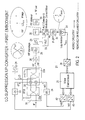
- fig.2 shows a block diagram of the system according to a first embodiment of the present invention;
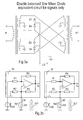
- fig.3a shows the equivalent circuit of a double-balanced mixer of fig.2;
- fig.3b shows the bias current injection circuits for the double-balanced mixer of fig.2;
- fig.4 shows the effective realization of a 38 GHz up-converter of fig.2;
- fig.5 shows a block diagram of the system according to a second embodiment of the present invention;
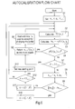
- fig.6 shows a flow chart of a possible autocalibration routine executed by a microcontroller of figures 2 and 5.
- With reference to fig.2, we see a circuitry built up around a single-sideband frequency up-
converter 20, also termed Image Rejection Mixer (IRM). TheIRM block 20 is well known in the art, see for example: - Watkins-Johnson Company - Tech-Notes, Vol. 12 No. 3, May/Jun 1985.
- Halford, B. R., "Single-Sideband Mixers for Communication Systems", 1982 IEEE MTT Symposiums Digest, pp. 30-32.
- The
IRM block 20 includes a double-balanced diode mixer 20' pumped by a LO sinusoidal signal generated by alocal oscillator 21, afirst quadrature hybrid 22a, and asecond quadrature hybrid 22b. Thefirst quadrature hybrid 22a operates as IF splitter connected to a balanced IF port of the double-balanced diode mixer 20'. Thesecond quadrature hybrid 22b operates as RF combiner connected to a balanced RF port of mixer 20', which also receives the unbalanced LO signal injected in-phase at a LO port. Two analog DC polarization blocks 23 and 24 individually controlled by aMixer Control block 25 are connected to respective biasing inputs of mixer 20'. The IF input signal is frequency converted by the IRM block into a single-sideband RF signal which undergoes a first amplification by aRF pre-amplifier 26. The latter is cascaded by an RFinterstage bandpass filter 28 and a variable-gaintransmission power amplifier 29.Bandpass filter 28 is not mandatory and when is used has relaxed out of band characteristic. TheTX power amplifier 29 is coupled to aRF power splitter 30 which splits the RF signal towards adiplexer filter 31 and a detection and control loop including a power detector andmixer diode 40 and an ALC block connected to the gain control input of theRF power amplifier 29. The spurious emission limits are always guaranteed bydiplexer filter 31. - The biasing calibration feedback loop includes the cascade of the following blocks: the
mixer 40, anIF bandpass filter 35, a Log-detector amplifier 41, an A/D converter 38, theMixer Control block 25, two D/A converters Component 40 is a diode pumped by the RF power so as to down-convert to IF at the output of the bandpass filter 35 (the IFBACK spectral line visible in the lowest ellipse) the residual of LO (LORES spectral line visible in the uppermost ellipse). Theelement 41 is a logarithmic amplifier operating as envelope detector of the down-converted IF power. A logarithmic amplifier is needed because of the large dynamic of the IF envelope due to dependence on the RTCP functionality. The output of the Log-detector amplifier 41 is a DC signal VREG directed to the A/D converter 38 at the input of themicrocontroller 25. The latter calculates two digital values Vd1 and Vd2 useful to update the diode mixer polarizations and forwards them to respective D/A converters - An equivalent circuit of a double-balanced mixer (corresponding to the block 20' inside the IRM 20) valid for the only signals excluded polarization is visible in fig.3a; the circuit includes two pairs of serially connected diodes D1, D2 and D3, D4. The two pairs of diodes are connected in counterphase and are fed at the centre of the two diodes with unbalanced LO signal. The RF and IF ports are both balanced with respect to ground. Fig.3b shows the circuital realization of the DC biasing blocks 23 and 24. With reference to fig.3b, the two
identical blocks Block 23 includes four resistors R1, R2, R3, and R4, of which: R3 and R4 are connected between the output Vo and the inputs + and -, respectively; R2 is connected between the input + and ground; R1 is connected to the output of D/A 43 and the input - of the operational in order to input the biasing voltage Vd1. The input + is further connected to a load Zd1 connected to ground, which corresponds to the resistance of a first pair of diodes included in the mixer 20'. Thanks to the given configuration and assuming the ratio R4/R1 = R3/R2, a biasing current Id1 = -Vd1/R2 independent of Zd1 flows through the load Zd1 and hence through the diodes. A biasing voltage Vp1 = Id1xZd1 is set across the load Zd1. The same conclusions are valid forDC block 24, respectively for Vd2, Id2, Zd2, and Vp2. - The real thin film implementation of a 38 GHz up-converter on alumina substrate is illustrated in fig.4.
- Fig.5 shows an alternative embodiment of the circuitry for the suppression of residual LO, where the same elements as in fig.2 are indicated by the same symbols. With reference to fig.5, we see that the circuitry represented in the left part of the figure and including the devices: 38, 25, 42, 43, 23, 24, 20, and 26 is the same as the corresponding part of fig.2. A
splitter 27 splits the RF signal at the output of the pre-amplifier 26 into two signals and forwards a first one to an ALC control part and a second one to a feedback biasing calibration loop. - The ALC loop is separated from the
splitter 27 by an RFinterstage bandpass filter 28 that is not mandatory and, if present, has relaxed out of band characteristic. The ALC loop includes a variable gainRF power amplifier 29 coupled to apower splitter 30 which splits the RF signal towards adiplexer filter 31 and a detection and control loop including apower detector diode 32 and an ALC block connected to the gain control input of theRX power amplifier 29. The spurious emission limits are always guaranteed bydiplexer filter 31. - The biasing calibration feedback loop includes the cascade of the following blocks: a
mixer 34 pumped by the RF signal, anIF bandpass filter 35, anIF amplifier 36, anIF detector 37, and blocks 38, 25, 42, 43, 23 and 24. As previously said, at the output ofmixer 34 an IFBACK intermediate frequency power which follows the residual power of LO is obtained. This IFBACK power is originated from the beating between residual LO from the system IF up-conversion and the RF signal as driving power. The output of theIF detector 37 is a DC signal VREG directed to the A/D converter 38 at the input of themicrocontroller 25. The latter calculates two digital values Vd1 and Vd2 for updating two bias voltages ofblock IRM 20, separately, and forwards them to the respective D/A converters - In operation, in order to optimize the symmetry of the mixer diodes and achieve good LO/RF isolation, the DC bias voltages of mixer diodes are separately adjusted. To describe the autocalibration technique, an experimental 38 GHz up-converter supporting 128 QAM modulated signal is used. In this case the IF input signal is -5 dBm at 350 MHz, the LO signal is +15 dBm at 38.35 GHz, the RF converted signal is 15 dBm at 38 GHz (Lower Side Band) and the LO signal leakage at output LOres is -15 dBm at 38 GHz, that is 30 dBc below the usefull RF signal. Our goal is to obtain 50 dBc below.
- The biasing calibration method is nearly the same for the two embodiments of the invention, so that the only one of fig.2 is discussed. As said before, the
ALC detector 40 acts as a down-converter mixer too, anyway in this case the pump signal is the RF signal and the ORES is the input signal. The downconverted signal is the regenerated IF signal IFBACK at 350 MHz with a power level of -50 dBm. This signal is linear related to the LORES signal; ifLO RES 1 dB decreases, IFBACK 1 dB dcreases too. The log-detector 41, which is fed by the IFBACK signal, generates a DC signal VREG that is used by themicrocontroller 25 to adjust the biasing of mixer diodes to improve LO signal output suppression. The log-detector is used in order to have a wide dynamic range and a high detection sensitivity. The microcontroller routine works according the following steps shown in fig.6. - With reference to fig.6, the
microcontroller 25 in standby status S1 is switched on in step S2 to start the LORES minimization routine based on the well known gradient method or one of its many variants, e.g.: steepest descent, conjugate gradient, etc. The aim of the method is to find a local minimum of a function f(x) iteratively, starting from an initial point x 0 and terminating only when the absolute gradient value falls below an ε value as small as whished. The argument of the object function f(x) is a n-dimensional vector x. In the concrete case, the function f is VREG(Id1, Id2); x is a vector [Id1, Id2]T, and x 0 = [Id10, Id20]T is a vector representing the initial working points of the diode pairs 20' as reported in the component data sheets. The function VREG(Id1, Id2) is achievable in known way from the following items: - • I(V) exponential characteristics of diodes used to set the working point of the double-balanced mixer;
- • physical model used to describe their radiofrequency behaviour of diodes;
- • power of the LO pump signal;
- • phase relations and frequency behaviour at the various ports of hybrids used by the single-sideband frequency converter;
- • gain of the various chained blocks;
- • bandpass response of the interstage filter;
- • conductance of the voltage-to-current converters.
- Instead of deriving the function VREG(Id1, Id2) by means of pure theoretical considerations, which is very difficult task, it can be experimentally derived interpolating through a grid of measures involving couple of bias currents and corresponding values of VREG. Several surface interpolating method using different form of interpolating functions are known in the literature, e.g. bilinear, bicubic polynomial functions. The descent gradient method includes the following steps:
- 1. (Step S1) - Set the initial polarization currents Id10, Id20 of diode pairs 20'. In order to better agree with iterative handling we pose: Id1k, Id2k (initial k = 0). Set the stop value ε and the initial learning factor η0. The stop value ε shall be selected in a way that LORES power reaches a target ≤ -50 dBc. The goal, conceptually achievable, corresponds to a good symmetry on the behaviour of the upconverter, but this doesn't necessarily means perfect equality of the two bias currents.
- 2. (Step S2) - Calculate ∇VREG(Id1k, Id2k), (∇ is the gradient operator) in point x k = [Id1k, Id2k ]:

- 3. (Step S3) - Calculate the displacement Δx k from point x k as:
Δx k = -η∇VREG (Id1k, Id2k ), where η > 0 is the learning factor, assumed to be very small so that the following inequality comes true: VREG(Id1k+1Id2k+1 ) ≤ VREG(Id1k,Id2k ). This means moving in the opposite direction in respect of the gradient. - 4. (Step S4) - If ∥η∇VREG (Id1k,Id2k )∥ ≤ ε, it results that x k = [Id1k,Id2k ] is a point of local minimum of the function VREG(Id1k,Id2k ); as a consequence the cycle is temporarily stopped.
- 5. (Step S5) - The couple x k ; f(x k ) is returned as minimum couple.
- 6. (Step S6) - A waiting time interval Tu is entered before a new minimization cycle is restarted (Step S2). Time Tu is in the order of few seconds to match with physical phenomena having effect on mixer unbalance, e.g. temperature and aging, are slow. Nevertheless in case the carrier is changed before time Tu is elapsed, the wait is interrupted and a new updating iteration introduced (Step S2). Whether the condition on ε is false the algorithm continues with the next updating step S7.
- 7. (Step S7) - Before calculating a new point, the current iteration number is compared to the maximum permissible number of iterations N1MAX to reach the convergence; in case of equality the actual x k; f(x k ) is returned as minimum couple.
- 8. (Step S8) - Calculate a new point x k+1 = x k + Δx k , that is:

- 9. (Step S9) - The condition: ∥∇VREG (Id1k ,Id2k ) ∥ < ∥∇ VREG (Id1k-1 ,Id2k-t ) ∥ is tested as a criterion to update the learning factor η in order to accelerate the convergence of the method (e.g. using Vogl's algorithm).
- 10. (Step S10) - If the condition checked in Step S9 is true the learning factor η is increased of a certain percentage β as greater as the difference between iterations k and k-1 of the module of gradient increases, and a new updating iteration is entered (Step S2).
- 11. (Step S11) - If the condition checked in Step S9 is false the learning factor η is decreased of a certain percentage β as greater as the difference between iterations k and k-1 of the module of gradient increases.
- 12. (Step S12) - The current iteration number is compared to the maximum permissible number of iterations N2MAX waiting for gradient reduction. If number N2MAX is not reached a new updating iteration is entered (Step S2).
- 13. (Step S13) - If the number N2MAX is reached another starting point is selected and a new minimization cycle is entered (Step S2).
- Although the invention has been described with particular reference to a preferred embodiment, it will be evident to those skilled in the art, that the present invention is not limited thereto, but further variations and modifications may be applied without departing from the scope thereof.
Claims (7)
- Method to improve local oscillator LO signal rejection in single-sideband radiofrequency up-converters (20) comprising a balanced or double-balanced mixer (20') biased with differential currents (Id1, Id2) adjustable to improve said rejection, characterized in that includes the following steps:a) down-converting the residual power of LO to intermediate frequency IF from the beating of said LO residual with the output RF signal used as driving power of an auxiliary mixer (34, 40);b) detecting (35, 36, 41, 37) the LO residual power down-converted to IF for obtaining in correspondence a quasi-continuous target voltage (VREG) to be minimized by means of any suitable known minimization method able to vary according to a predetermined strategy one or more physical parameter of said up-converters (20), such as said bias current values (Id1, Id2), or the IF and/or RF phase at relevant ports and evaluating in correspondence the effect on said target voltage.
- The method of claim 1, characterized in that said step b) includes:c) setting initial bias current values to start a minimization cycle of said target voltage mathematically describable by means of a f(Id1, Id2) function of said bias currents Id1, Id2; the cycle including the following iterative updating steps indicated by index k;d) calculating (25) the gradient of f(Id1k, Id2k) with respect to the two bias currents Id1k, Id2k, multiplying the gradient by a learning factor η > 0 and changing the sign of the product in order to find a vectorial variation for updating the bias currents;e) comparing the module of said vectorial variation with a predetermined threshold ∈ in correspondence of which the power of residual LO is equal to a target value, and stopping to update the bias currents when said module reaches the threshold ∈;f) calculating next values of the bias currents summing up said vectorial variation to the actual values of the bias currents Id1k, Id2k and introducing a new updating iteration from step d).
- The method of claim 21, characterized in that said function f(Id1, Id2) is derived by pure theoretical considerations.
- The method of claim 2, characterized in that said function f(ld1, ld2) is experimentally derived interpolating through a grid of measures involving couple of bias currents Id1k, Id2k and corresponding quasi-continuous voltage values obtained by the LO residual power down-converted to IF.
- System to improve local oscillator LO signal rejection in single-sideband radiofrequency up-converter (20) comprising:• a balanced or double-balanced mixer (20') biased with differential currents (Id1, Id2);• means for calibrating the bias currents (Id1, Id2) in order to improve local oscillator LO signal rejection,characterized in that said calibrating means belongs to a feedback loop including:• a radiofrequency RF power splitter (27, 30) connected downstream the up-converter (20) in order to derive an RF power towards an auxiliary mixer (34, 40) for generating back an intermediate frequency power IF from the beating between the LO residual power and the RF signal used as driving power;• detection means (36, 37, 41) of said generated back IF power outputting a regulation voltage level (VREG) ;• control means (25) for minimizing said regulation voltage level (VREG), and hence the residual power of LO, according to any known minimization method able to calculates pairs of optimal bias voltages (Vd1, Vd2);• voltage-to-current conversion means (32, 24) placed downstream said control means (20) for obtaining said bias currents (Id1, Id2).
- The system of claim 5, characterized in that said auxiliary mixer (40) also constitutes the RF detector of an automatic level control loop (ALC) driven by the RF signal power at the output of a final power amplifier (29).
- The up-converter of claim 6, characterized in that said detection means includes a logarithmic amplifier (41) outputting said regulation voltage level (VREG).
Priority Applications (2)
| Application Number | Priority Date | Filing Date | Title |
|---|---|---|---|
| AT06425224T ATE515828T1 (en) | 2006-03-31 | 2006-03-31 | TRANSMITTER WITH SUPPRESSED CARRIER AND METHOD THEREOF |
| EP06425224A EP1841058B1 (en) | 2006-03-31 | 2006-03-31 | Method and system to improve local oscillator signal rejection in single-sideband radiofrequency up-converters |
Applications Claiming Priority (1)
| Application Number | Priority Date | Filing Date | Title |
|---|---|---|---|
| EP06425224A EP1841058B1 (en) | 2006-03-31 | 2006-03-31 | Method and system to improve local oscillator signal rejection in single-sideband radiofrequency up-converters |
Publications (2)
| Publication Number | Publication Date |
|---|---|
| EP1841058A1 true EP1841058A1 (en) | 2007-10-03 |
| EP1841058B1 EP1841058B1 (en) | 2011-07-06 |
Family
ID=36591293
Family Applications (1)
| Application Number | Title | Priority Date | Filing Date |
|---|---|---|---|
| EP06425224A Expired - Lifetime EP1841058B1 (en) | 2006-03-31 | 2006-03-31 | Method and system to improve local oscillator signal rejection in single-sideband radiofrequency up-converters |
Country Status (2)
| Country | Link |
|---|---|
| EP (1) | EP1841058B1 (en) |
| AT (1) | ATE515828T1 (en) |
Cited By (5)
| Publication number | Priority date | Publication date | Assignee | Title |
|---|---|---|---|---|
| WO2011131229A1 (en) | 2010-04-20 | 2011-10-27 | Nokia Siemens Networks Oy | Method and device for data processing |
| CN104052507A (en) * | 2013-03-14 | 2014-09-17 | 美国亚德诺半导体公司 | Transmitter LO leakage calibration scheme using loopback circuitry |
| US8854124B2 (en) | 2011-11-07 | 2014-10-07 | Electronics And Telecommunications Research Institute | Envelope detector |
| CN114924242A (en) * | 2022-04-21 | 2022-08-19 | 中星联华科技(北京)有限公司 | ALC open-loop calibration method and device for microwave analog signal source |
| CN117792841A (en) * | 2024-02-28 | 2024-03-29 | 南京迈创立电子科技有限公司 | A local oscillator leakage self-calibration system and method based on multi-dimensional gradient descent |
Families Citing this family (1)
| Publication number | Priority date | Publication date | Assignee | Title |
|---|---|---|---|---|
| TWI487402B (en) * | 2012-08-10 | 2015-06-01 | Mstar Semiconductor Inc | Searching method for radio frequency communication system |
Citations (6)
| Publication number | Priority date | Publication date | Assignee | Title |
|---|---|---|---|---|
| US5162763A (en) * | 1991-11-18 | 1992-11-10 | Morris Keith D | Single sideband modulator for translating baseband signals to radio frequency in single stage |
| US5343171A (en) * | 1992-09-28 | 1994-08-30 | Kabushiki Kaish Toshiba | Circuit for improving carrier rejection in a balanced modulator |
| EP0661801A1 (en) * | 1993-12-29 | 1995-07-05 | AT&T Corp. | Quadrature modulator with adaptive suppression of carrier leakage |
| US5903823A (en) * | 1995-09-19 | 1999-05-11 | Fujitsu Limited | Radio apparatus with distortion compensating function |
| US6169463B1 (en) * | 1999-03-24 | 2001-01-02 | Philips Electronic North America Corp. | Quadrature modulator with set-and-forget carrier leakage compensation |
| US6720839B1 (en) * | 2000-02-29 | 2004-04-13 | Skyworks Solutions, Inc. | System of and method for reducing or eliminating the unwanted sideband in a signal derived from the output of a quadrature modulator |
-
2006
- 2006-03-31 AT AT06425224T patent/ATE515828T1/en not_active IP Right Cessation
- 2006-03-31 EP EP06425224A patent/EP1841058B1/en not_active Expired - Lifetime
Patent Citations (6)
| Publication number | Priority date | Publication date | Assignee | Title |
|---|---|---|---|---|
| US5162763A (en) * | 1991-11-18 | 1992-11-10 | Morris Keith D | Single sideband modulator for translating baseband signals to radio frequency in single stage |
| US5343171A (en) * | 1992-09-28 | 1994-08-30 | Kabushiki Kaish Toshiba | Circuit for improving carrier rejection in a balanced modulator |
| EP0661801A1 (en) * | 1993-12-29 | 1995-07-05 | AT&T Corp. | Quadrature modulator with adaptive suppression of carrier leakage |
| US5903823A (en) * | 1995-09-19 | 1999-05-11 | Fujitsu Limited | Radio apparatus with distortion compensating function |
| US6169463B1 (en) * | 1999-03-24 | 2001-01-02 | Philips Electronic North America Corp. | Quadrature modulator with set-and-forget carrier leakage compensation |
| US6720839B1 (en) * | 2000-02-29 | 2004-04-13 | Skyworks Solutions, Inc. | System of and method for reducing or eliminating the unwanted sideband in a signal derived from the output of a quadrature modulator |
Cited By (7)
| Publication number | Priority date | Publication date | Assignee | Title |
|---|---|---|---|---|
| WO2011131229A1 (en) | 2010-04-20 | 2011-10-27 | Nokia Siemens Networks Oy | Method and device for data processing |
| US8854124B2 (en) | 2011-11-07 | 2014-10-07 | Electronics And Telecommunications Research Institute | Envelope detector |
| CN104052507A (en) * | 2013-03-14 | 2014-09-17 | 美国亚德诺半导体公司 | Transmitter LO leakage calibration scheme using loopback circuitry |
| CN104052507B (en) * | 2013-03-14 | 2017-04-26 | 美国亚德诺半导体公司 | Circuitry and method for detecting and correcting transmitter LO leakage using loopback circuitry |
| US9787415B2 (en) | 2013-03-14 | 2017-10-10 | Analog Devices, Inc. | Transmitter LO leakage calibration scheme using loopback circuitry |
| CN114924242A (en) * | 2022-04-21 | 2022-08-19 | 中星联华科技(北京)有限公司 | ALC open-loop calibration method and device for microwave analog signal source |
| CN117792841A (en) * | 2024-02-28 | 2024-03-29 | 南京迈创立电子科技有限公司 | A local oscillator leakage self-calibration system and method based on multi-dimensional gradient descent |
Also Published As
| Publication number | Publication date |
|---|---|
| ATE515828T1 (en) | 2011-07-15 |
| EP1841058B1 (en) | 2011-07-06 |
Similar Documents
| Publication | Publication Date | Title |
|---|---|---|
| US7058139B2 (en) | Transmitter with transmitter chain phase adjustment on the basis of pre-stored phase information | |
| US8526896B2 (en) | Feedback compensation detector for a direct conversion transmitter | |
| US7027785B2 (en) | Transmitter RF power control | |
| US5508657A (en) | Feed forward cancellation amplifier utilizing dynamic vector control | |
| US8451942B2 (en) | Wireless transmission apparatus using cartesian loop | |
| US8140038B2 (en) | Adaptive receivers | |
| US20080014873A1 (en) | Methods and apparatus for adaptive local oscillator nulling | |
| US20070129025A1 (en) | Open loop polar transmitter having on-chip calibration | |
| CN109428616B (en) | Apparatus and method for radio frequency transmitter to compensate for local oscillator leakage | |
| KR20020056873A (en) | Parallel amplifier architecture using digital phase control techniques | |
| KR20000029152A (en) | Feedforward amplification system having mask detection compensation | |
| US12088331B2 (en) | Signal transmitting method and apparatus, electronic device, and readable storage medium | |
| US6614299B2 (en) | Method and system for automated current balance adjustment for parallel combined amplification elements | |
| CN220207791U (en) | Radio frequency testing machine and radio frequency testing system | |
| CN116366059B (en) | Radio frequency power synthesis circuit and method | |
| KR20000029154A (en) | Amplification system having mask detection | |
| US7164313B2 (en) | Method and apparatus for opening a feedback loop | |
| US7250815B2 (en) | Amplifier distortion management apparatus, systems, and methods | |
| EP1841058B1 (en) | Method and system to improve local oscillator signal rejection in single-sideband radiofrequency up-converters | |
| US12301172B2 (en) | Power amplifier linearizing module and power amplifier system equipped therewith | |
| US8160533B2 (en) | Self-calibrating mixer | |
| US7026874B2 (en) | Methods and apparatus for improving the operation of a variable gain amplifier (VGA) | |
| US7839230B2 (en) | PLL oscillation circuit, polar transmitting circuit, and communication device | |
| WO2000010247A1 (en) | Error correction in amplifiers | |
| US8923443B2 (en) | Wireless receiver |
Legal Events
| Date | Code | Title | Description |
|---|---|---|---|
| PUAI | Public reference made under article 153(3) epc to a published international application that has entered the european phase |
Free format text: ORIGINAL CODE: 0009012 |
|
| AK | Designated contracting states |
Kind code of ref document: A1 Designated state(s): AT BE BG CH CY CZ DE DK EE ES FI FR GB GR HU IE IS IT LI LT LU LV MC NL PL PT RO SE SI SK TR |
|
| AX | Request for extension of the european patent |
Extension state: AL BA HR MK YU |
|
| 17P | Request for examination filed |
Effective date: 20080403 |
|
| 17Q | First examination report despatched |
Effective date: 20080513 |
|
| AKX | Designation fees paid |
Designated state(s): AT BE BG CH CY CZ DE DK EE ES FI FR GB GR HU IE IS IT LI LT LU LV MC NL PL PT RO SE SI SK TR |
|
| RAP1 | Party data changed (applicant data changed or rights of an application transferred) |
Owner name: NOKIA SIEMENS NETWORKS S.P.A. |
|
| GRAJ | Information related to disapproval of communication of intention to grant by the applicant or resumption of examination proceedings by the epo deleted |
Free format text: ORIGINAL CODE: EPIDOSDIGR1 |
|
| GRAP | Despatch of communication of intention to grant a patent |
Free format text: ORIGINAL CODE: EPIDOSNIGR1 |
|
| GRAP | Despatch of communication of intention to grant a patent |
Free format text: ORIGINAL CODE: EPIDOSNIGR1 |
|
| GRAS | Grant fee paid |
Free format text: ORIGINAL CODE: EPIDOSNIGR3 |
|
| GRAA | (expected) grant |
Free format text: ORIGINAL CODE: 0009210 |
|
| AK | Designated contracting states |
Kind code of ref document: B1 Designated state(s): AT BE BG CH CY CZ DE DK EE ES FI FR GB GR HU IE IS IT LI LT LU LV MC NL PL PT RO SE SI SK TR |
|
| REG | Reference to a national code |
Ref country code: GB Ref legal event code: FG4D |
|
| REG | Reference to a national code |
Ref country code: CH Ref legal event code: EP |
|
| REG | Reference to a national code |
Ref country code: IE Ref legal event code: FG4D |
|
| REG | Reference to a national code |
Ref country code: DE Ref legal event code: R096 Ref document number: 602006022905 Country of ref document: DE Effective date: 20110901 |
|
| REG | Reference to a national code |
Ref country code: NL Ref legal event code: VDEP Effective date: 20110706 |
|
| PG25 | Lapsed in a contracting state [announced via postgrant information from national office to epo] |
Ref country code: SI Free format text: LAPSE BECAUSE OF FAILURE TO SUBMIT A TRANSLATION OF THE DESCRIPTION OR TO PAY THE FEE WITHIN THE PRESCRIBED TIME-LIMIT Effective date: 20110706 |
|
| REG | Reference to a national code |
Ref country code: AT Ref legal event code: MK05 Ref document number: 515828 Country of ref document: AT Kind code of ref document: T Effective date: 20110706 |
|
| PG25 | Lapsed in a contracting state [announced via postgrant information from national office to epo] |
Ref country code: SE Free format text: LAPSE BECAUSE OF FAILURE TO SUBMIT A TRANSLATION OF THE DESCRIPTION OR TO PAY THE FEE WITHIN THE PRESCRIBED TIME-LIMIT Effective date: 20110706 Ref country code: PT Free format text: LAPSE BECAUSE OF FAILURE TO SUBMIT A TRANSLATION OF THE DESCRIPTION OR TO PAY THE FEE WITHIN THE PRESCRIBED TIME-LIMIT Effective date: 20111107 Ref country code: BE Free format text: LAPSE BECAUSE OF FAILURE TO SUBMIT A TRANSLATION OF THE DESCRIPTION OR TO PAY THE FEE WITHIN THE PRESCRIBED TIME-LIMIT Effective date: 20110706 Ref country code: FI Free format text: LAPSE BECAUSE OF FAILURE TO SUBMIT A TRANSLATION OF THE DESCRIPTION OR TO PAY THE FEE WITHIN THE PRESCRIBED TIME-LIMIT Effective date: 20110706 Ref country code: NL Free format text: LAPSE BECAUSE OF FAILURE TO SUBMIT A TRANSLATION OF THE DESCRIPTION OR TO PAY THE FEE WITHIN THE PRESCRIBED TIME-LIMIT Effective date: 20110706 Ref country code: LT Free format text: LAPSE BECAUSE OF FAILURE TO SUBMIT A TRANSLATION OF THE DESCRIPTION OR TO PAY THE FEE WITHIN THE PRESCRIBED TIME-LIMIT Effective date: 20110706 Ref country code: IS Free format text: LAPSE BECAUSE OF FAILURE TO SUBMIT A TRANSLATION OF THE DESCRIPTION OR TO PAY THE FEE WITHIN THE PRESCRIBED TIME-LIMIT Effective date: 20111106 |
|
| PG25 | Lapsed in a contracting state [announced via postgrant information from national office to epo] |
Ref country code: CY Free format text: LAPSE BECAUSE OF FAILURE TO SUBMIT A TRANSLATION OF THE DESCRIPTION OR TO PAY THE FEE WITHIN THE PRESCRIBED TIME-LIMIT Effective date: 20110706 Ref country code: PL Free format text: LAPSE BECAUSE OF FAILURE TO SUBMIT A TRANSLATION OF THE DESCRIPTION OR TO PAY THE FEE WITHIN THE PRESCRIBED TIME-LIMIT Effective date: 20110706 Ref country code: LV Free format text: LAPSE BECAUSE OF FAILURE TO SUBMIT A TRANSLATION OF THE DESCRIPTION OR TO PAY THE FEE WITHIN THE PRESCRIBED TIME-LIMIT Effective date: 20110706 Ref country code: AT Free format text: LAPSE BECAUSE OF FAILURE TO SUBMIT A TRANSLATION OF THE DESCRIPTION OR TO PAY THE FEE WITHIN THE PRESCRIBED TIME-LIMIT Effective date: 20110706 |
|
| PG25 | Lapsed in a contracting state [announced via postgrant information from national office to epo] |
Ref country code: SK Free format text: LAPSE BECAUSE OF FAILURE TO SUBMIT A TRANSLATION OF THE DESCRIPTION OR TO PAY THE FEE WITHIN THE PRESCRIBED TIME-LIMIT Effective date: 20110706 Ref country code: CZ Free format text: LAPSE BECAUSE OF FAILURE TO SUBMIT A TRANSLATION OF THE DESCRIPTION OR TO PAY THE FEE WITHIN THE PRESCRIBED TIME-LIMIT Effective date: 20110706 |
|
| PLBE | No opposition filed within time limit |
Free format text: ORIGINAL CODE: 0009261 |
|
| STAA | Information on the status of an ep patent application or granted ep patent |
Free format text: STATUS: NO OPPOSITION FILED WITHIN TIME LIMIT |
|
| PG25 | Lapsed in a contracting state [announced via postgrant information from national office to epo] |
Ref country code: RO Free format text: LAPSE BECAUSE OF FAILURE TO SUBMIT A TRANSLATION OF THE DESCRIPTION OR TO PAY THE FEE WITHIN THE PRESCRIBED TIME-LIMIT Effective date: 20110706 Ref country code: EE Free format text: LAPSE BECAUSE OF FAILURE TO SUBMIT A TRANSLATION OF THE DESCRIPTION OR TO PAY THE FEE WITHIN THE PRESCRIBED TIME-LIMIT Effective date: 20110706 |
|
| 26N | No opposition filed |
Effective date: 20120411 |
|
| PG25 | Lapsed in a contracting state [announced via postgrant information from national office to epo] |
Ref country code: DK Free format text: LAPSE BECAUSE OF FAILURE TO SUBMIT A TRANSLATION OF THE DESCRIPTION OR TO PAY THE FEE WITHIN THE PRESCRIBED TIME-LIMIT Effective date: 20110706 |
|
| REG | Reference to a national code |
Ref country code: DE Ref legal event code: R097 Ref document number: 602006022905 Country of ref document: DE Effective date: 20120411 |
|
| REG | Reference to a national code |
Ref country code: GB Ref legal event code: 732E Free format text: REGISTERED BETWEEN 20120719 AND 20120725 |
|
| REG | Reference to a national code |
Ref country code: DE Ref legal event code: R081 Ref document number: 602006022905 Country of ref document: DE Owner name: DRAGONWAVE S.A R.L., LU Free format text: FORMER OWNER: SIEMENS S.P.A., MAILAND/MILANO, IT Effective date: 20110712 Ref country code: DE Ref legal event code: R081 Ref document number: 602006022905 Country of ref document: DE Owner name: DRAGONWAVE S.A R.L., LU Free format text: FORMER OWNER: NOKIA SIEMENS NETWORKS S.P.A., CASSINA DE' PECCHI, MILANO, IT Effective date: 20120731 Ref country code: DE Ref legal event code: R081 Ref document number: 602006022905 Country of ref document: DE Owner name: NOKIA SIEMENS NETWORKS ITALIA S.P.A., IT Free format text: FORMER OWNER: SIEMENS S.P.A., MAILAND/MILANO, IT Effective date: 20110712 Ref country code: DE Ref legal event code: R081 Ref document number: 602006022905 Country of ref document: DE Owner name: NOKIA SIEMENS NETWORKS ITALIA S.P.A., IT Free format text: FORMER OWNER: NOKIA SIEMENS NETWORKS S.P.A., CASSINA DE' PECCHI, IT Effective date: 20120731 Ref country code: DE Ref legal event code: R081 Ref document number: 602006022905 Country of ref document: DE Owner name: NOKIA SIEMENS NETWORKS ITALIA S.P.A., IT Free format text: FORMER OWNER: NOKIA SIEMENS NETWORKS S.P.A., CASSINA DE' PECCHI, MILANO, IT Effective date: 20120731 |
|
| PG25 | Lapsed in a contracting state [announced via postgrant information from national office to epo] |
Ref country code: MC Free format text: LAPSE BECAUSE OF NON-PAYMENT OF DUE FEES Effective date: 20120331 |
|
| REG | Reference to a national code |
Ref country code: CH Ref legal event code: PL |
|
| REG | Reference to a national code |
Ref country code: IE Ref legal event code: MM4A |
|
| PG25 | Lapsed in a contracting state [announced via postgrant information from national office to epo] |
Ref country code: CH Free format text: LAPSE BECAUSE OF NON-PAYMENT OF DUE FEES Effective date: 20120331 Ref country code: IE Free format text: LAPSE BECAUSE OF NON-PAYMENT OF DUE FEES Effective date: 20120331 Ref country code: LI Free format text: LAPSE BECAUSE OF NON-PAYMENT OF DUE FEES Effective date: 20120331 |
|
| PG25 | Lapsed in a contracting state [announced via postgrant information from national office to epo] |
Ref country code: ES Free format text: LAPSE BECAUSE OF FAILURE TO SUBMIT A TRANSLATION OF THE DESCRIPTION OR TO PAY THE FEE WITHIN THE PRESCRIBED TIME-LIMIT Effective date: 20111017 |
|
| PGFP | Annual fee paid to national office [announced via postgrant information from national office to epo] |
Ref country code: GB Payment date: 20130321 Year of fee payment: 8 Ref country code: FR Payment date: 20130408 Year of fee payment: 8 |
|
| REG | Reference to a national code |
Ref country code: FR Ref legal event code: CA Effective date: 20130426 Ref country code: FR Ref legal event code: CD Owner name: NOKIA SIEMENS NETWORKS ITALIA S.P.A., IT Effective date: 20130426 |
|
| PG25 | Lapsed in a contracting state [announced via postgrant information from national office to epo] |
Ref country code: BG Free format text: LAPSE BECAUSE OF FAILURE TO SUBMIT A TRANSLATION OF THE DESCRIPTION OR TO PAY THE FEE WITHIN THE PRESCRIBED TIME-LIMIT Effective date: 20111006 |
|
| REG | Reference to a national code |
Ref country code: FR Ref legal event code: TP Owner name: NOKIA SIEMENS NETWORKS ITALIA S.P.A., IT Effective date: 20130607 |
|
| PG25 | Lapsed in a contracting state [announced via postgrant information from national office to epo] |
Ref country code: TR Free format text: LAPSE BECAUSE OF FAILURE TO SUBMIT A TRANSLATION OF THE DESCRIPTION OR TO PAY THE FEE WITHIN THE PRESCRIBED TIME-LIMIT Effective date: 20110706 |
|
| PG25 | Lapsed in a contracting state [announced via postgrant information from national office to epo] |
Ref country code: LU Free format text: LAPSE BECAUSE OF NON-PAYMENT OF DUE FEES Effective date: 20120331 |
|
| PG25 | Lapsed in a contracting state [announced via postgrant information from national office to epo] |
Ref country code: HU Free format text: LAPSE BECAUSE OF FAILURE TO SUBMIT A TRANSLATION OF THE DESCRIPTION OR TO PAY THE FEE WITHIN THE PRESCRIBED TIME-LIMIT Effective date: 20060331 |
|
| PG25 | Lapsed in a contracting state [announced via postgrant information from national office to epo] |
Ref country code: GR Free format text: LAPSE BECAUSE OF FAILURE TO SUBMIT A TRANSLATION OF THE DESCRIPTION OR TO PAY THE FEE WITHIN THE PRESCRIBED TIME-LIMIT Effective date: 20110706 |
|
| GBPC | Gb: european patent ceased through non-payment of renewal fee |
Effective date: 20140331 |
|
| REG | Reference to a national code |
Ref country code: FR Ref legal event code: ST Effective date: 20141128 |
|
| PG25 | Lapsed in a contracting state [announced via postgrant information from national office to epo] |
Ref country code: GB Free format text: LAPSE BECAUSE OF NON-PAYMENT OF DUE FEES Effective date: 20140331 Ref country code: FR Free format text: LAPSE BECAUSE OF NON-PAYMENT OF DUE FEES Effective date: 20140331 |
|
| PG25 | Lapsed in a contracting state [announced via postgrant information from national office to epo] |
Ref country code: IT Free format text: LAPSE BECAUSE OF NON-PAYMENT OF DUE FEES Effective date: 20160331 |
|
| REG | Reference to a national code |
Ref country code: DE Ref legal event code: R081 Ref document number: 602006022905 Country of ref document: DE Owner name: DRAGONWAVE S.A R.L., LU Free format text: FORMER OWNER: NOKIA SIEMENS NETWORKS ITALIA S.P.A., CASSINA DE PECCHI, IT |
|
| PGFP | Annual fee paid to national office [announced via postgrant information from national office to epo] |
Ref country code: DE Payment date: 20170330 Year of fee payment: 12 |
|
| PG25 | Lapsed in a contracting state [announced via postgrant information from national office to epo] |
Ref country code: IT Free format text: LAPSE BECAUSE OF NON-PAYMENT OF DUE FEES Effective date: 20160331 |
|
| PGRI | Patent reinstated in contracting state [announced from national office to epo] |
Ref country code: IT Effective date: 20170710 |
|
| PGFP | Annual fee paid to national office [announced via postgrant information from national office to epo] |
Ref country code: IT Payment date: 20170331 Year of fee payment: 12 |
|
| REG | Reference to a national code |
Ref country code: DE Ref legal event code: R119 Ref document number: 602006022905 Country of ref document: DE |
|
| PG25 | Lapsed in a contracting state [announced via postgrant information from national office to epo] |
Ref country code: DE Free format text: LAPSE BECAUSE OF NON-PAYMENT OF DUE FEES Effective date: 20181002 |
|
| PG25 | Lapsed in a contracting state [announced via postgrant information from national office to epo] |
Ref country code: IT Free format text: LAPSE BECAUSE OF NON-PAYMENT OF DUE FEES Effective date: 20180331 |