EP1840866A2 - Pixel and organic light emitting display device using the pixel - Google Patents
Pixel and organic light emitting display device using the pixel Download PDFInfo
- Publication number
- EP1840866A2 EP1840866A2 EP07251346A EP07251346A EP1840866A2 EP 1840866 A2 EP1840866 A2 EP 1840866A2 EP 07251346 A EP07251346 A EP 07251346A EP 07251346 A EP07251346 A EP 07251346A EP 1840866 A2 EP1840866 A2 EP 1840866A2
- Authority
- EP
- European Patent Office
- Prior art keywords
- transistor
- electrode
- light emitting
- voltage
- scan
- Prior art date
- Legal status (The legal status is an assumption and is not a legal conclusion. Google has not performed a legal analysis and makes no representation as to the accuracy of the status listed.)
- Granted
Links
- 239000003990 capacitor Substances 0.000 claims abstract description 37
- 238000010586 diagram Methods 0.000 description 13
- 101100060016 Mus musculus Chst3 gene Proteins 0.000 description 10
- 238000000034 method Methods 0.000 description 3
- 230000001360 synchronised effect Effects 0.000 description 2
- 230000003247 decreasing effect Effects 0.000 description 1
- 238000004519 manufacturing process Methods 0.000 description 1
- 238000012986 modification Methods 0.000 description 1
- 230000004048 modification Effects 0.000 description 1
- 230000000630 rising effect Effects 0.000 description 1
Images


Classifications
-
- G—PHYSICS
- G09—EDUCATION; CRYPTOGRAPHY; DISPLAY; ADVERTISING; SEALS
- G09G—ARRANGEMENTS OR CIRCUITS FOR CONTROL OF INDICATING DEVICES USING STATIC MEANS TO PRESENT VARIABLE INFORMATION
- G09G3/00—Control arrangements or circuits, of interest only in connection with visual indicators other than cathode-ray tubes
- G09G3/20—Control arrangements or circuits, of interest only in connection with visual indicators other than cathode-ray tubes for presentation of an assembly of a number of characters, e.g. a page, by composing the assembly by combination of individual elements arranged in a matrix no fixed position being assigned to or needed to be assigned to the individual characters or partial characters
- G09G3/22—Control arrangements or circuits, of interest only in connection with visual indicators other than cathode-ray tubes for presentation of an assembly of a number of characters, e.g. a page, by composing the assembly by combination of individual elements arranged in a matrix no fixed position being assigned to or needed to be assigned to the individual characters or partial characters using controlled light sources
- G09G3/30—Control arrangements or circuits, of interest only in connection with visual indicators other than cathode-ray tubes for presentation of an assembly of a number of characters, e.g. a page, by composing the assembly by combination of individual elements arranged in a matrix no fixed position being assigned to or needed to be assigned to the individual characters or partial characters using controlled light sources using electroluminescent panels
- G09G3/32—Control arrangements or circuits, of interest only in connection with visual indicators other than cathode-ray tubes for presentation of an assembly of a number of characters, e.g. a page, by composing the assembly by combination of individual elements arranged in a matrix no fixed position being assigned to or needed to be assigned to the individual characters or partial characters using controlled light sources using electroluminescent panels semiconductive, e.g. using light-emitting diodes [LED]
- G09G3/3208—Control arrangements or circuits, of interest only in connection with visual indicators other than cathode-ray tubes for presentation of an assembly of a number of characters, e.g. a page, by composing the assembly by combination of individual elements arranged in a matrix no fixed position being assigned to or needed to be assigned to the individual characters or partial characters using controlled light sources using electroluminescent panels semiconductive, e.g. using light-emitting diodes [LED] organic, e.g. using organic light-emitting diodes [OLED]
- G09G3/3225—Control arrangements or circuits, of interest only in connection with visual indicators other than cathode-ray tubes for presentation of an assembly of a number of characters, e.g. a page, by composing the assembly by combination of individual elements arranged in a matrix no fixed position being assigned to or needed to be assigned to the individual characters or partial characters using controlled light sources using electroluminescent panels semiconductive, e.g. using light-emitting diodes [LED] organic, e.g. using organic light-emitting diodes [OLED] using an active matrix
- G09G3/3233—Control arrangements or circuits, of interest only in connection with visual indicators other than cathode-ray tubes for presentation of an assembly of a number of characters, e.g. a page, by composing the assembly by combination of individual elements arranged in a matrix no fixed position being assigned to or needed to be assigned to the individual characters or partial characters using controlled light sources using electroluminescent panels semiconductive, e.g. using light-emitting diodes [LED] organic, e.g. using organic light-emitting diodes [OLED] using an active matrix with pixel circuitry controlling the current through the light-emitting element
-
- G—PHYSICS
- G09—EDUCATION; CRYPTOGRAPHY; DISPLAY; ADVERTISING; SEALS
- G09G—ARRANGEMENTS OR CIRCUITS FOR CONTROL OF INDICATING DEVICES USING STATIC MEANS TO PRESENT VARIABLE INFORMATION
- G09G3/00—Control arrangements or circuits, of interest only in connection with visual indicators other than cathode-ray tubes
- G09G3/20—Control arrangements or circuits, of interest only in connection with visual indicators other than cathode-ray tubes for presentation of an assembly of a number of characters, e.g. a page, by composing the assembly by combination of individual elements arranged in a matrix no fixed position being assigned to or needed to be assigned to the individual characters or partial characters
- G09G3/22—Control arrangements or circuits, of interest only in connection with visual indicators other than cathode-ray tubes for presentation of an assembly of a number of characters, e.g. a page, by composing the assembly by combination of individual elements arranged in a matrix no fixed position being assigned to or needed to be assigned to the individual characters or partial characters using controlled light sources
- G09G3/30—Control arrangements or circuits, of interest only in connection with visual indicators other than cathode-ray tubes for presentation of an assembly of a number of characters, e.g. a page, by composing the assembly by combination of individual elements arranged in a matrix no fixed position being assigned to or needed to be assigned to the individual characters or partial characters using controlled light sources using electroluminescent panels
-
- G—PHYSICS
- G09—EDUCATION; CRYPTOGRAPHY; DISPLAY; ADVERTISING; SEALS
- G09G—ARRANGEMENTS OR CIRCUITS FOR CONTROL OF INDICATING DEVICES USING STATIC MEANS TO PRESENT VARIABLE INFORMATION
- G09G2300/00—Aspects of the constitution of display devices
- G09G2300/04—Structural and physical details of display devices
- G09G2300/0439—Pixel structures
- G09G2300/0465—Improved aperture ratio, e.g. by size reduction of the pixel circuit, e.g. for improving the pixel density or the maximum displayable luminance or brightness
-
- G—PHYSICS
- G09—EDUCATION; CRYPTOGRAPHY; DISPLAY; ADVERTISING; SEALS
- G09G—ARRANGEMENTS OR CIRCUITS FOR CONTROL OF INDICATING DEVICES USING STATIC MEANS TO PRESENT VARIABLE INFORMATION
- G09G2300/00—Aspects of the constitution of display devices
- G09G2300/08—Active matrix structure, i.e. with use of active elements, inclusive of non-linear two terminal elements, in the pixels together with light emitting or modulating elements
- G09G2300/0809—Several active elements per pixel in active matrix panels
- G09G2300/0819—Several active elements per pixel in active matrix panels used for counteracting undesired variations, e.g. feedback or autozeroing
-
- G—PHYSICS
- G09—EDUCATION; CRYPTOGRAPHY; DISPLAY; ADVERTISING; SEALS
- G09G—ARRANGEMENTS OR CIRCUITS FOR CONTROL OF INDICATING DEVICES USING STATIC MEANS TO PRESENT VARIABLE INFORMATION
- G09G2300/00—Aspects of the constitution of display devices
- G09G2300/08—Active matrix structure, i.e. with use of active elements, inclusive of non-linear two terminal elements, in the pixels together with light emitting or modulating elements
- G09G2300/0809—Several active elements per pixel in active matrix panels
- G09G2300/0842—Several active elements per pixel in active matrix panels forming a memory circuit, e.g. a dynamic memory with one capacitor
- G09G2300/0861—Several active elements per pixel in active matrix panels forming a memory circuit, e.g. a dynamic memory with one capacitor with additional control of the display period without amending the charge stored in a pixel memory, e.g. by means of additional select electrodes
Definitions
- the present invention relates to a pixel and an organic light emitting display device using the pixel. More particularly, the present invention relates to a pixel and an organic light emitting display device using the pixel which has a minimal number of transistors to display images of uniform brightness.
- OLED organic light emitting diode
- An OLED generates light by recombining electrons and holes.
- Advantages of organic light emitting display devices include low power consumption as well as rapid response speed.
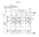
- FIG. 1 is a circuit diagram showing a pixel of a conventional organic light emitting display device.
- the pixel 4 includes a pixel circuit 2 connected to an OLED, to a data line Dm, and to a scan line Sn for controlling the OLED.
- An anode electrode of the OLED is connected with the pixel circuit 2, and a cathode electrode of the OLED is connected to a power source ELVSS.
- the OLED generates light of a certain or predetermined brightness corresponding to a level of a current supplied to the OLED from the pixel circuit 2.
- the pixel circuit 2 controls the level of the current supplied to the OLED corresponding to a data signal supplied to the data line Dm, when a scan signal is supplied to the scan line Sn.
- the pixel circuit 2 includes a first transistor M11 and a second transistor M12.
- the second transistor M12 is connected between a power source ELVDD and the OLED.
- the first transistor M11 is connected with the second transistor M12, with the data line Dm, and with the scan line Sn.
- the pixel circuit 2 further includes a storage capacitor C 1 st connected between a gate electrode and a first electrode of the second transistor M 12.
- a gate electrode of the first transistor M11 is connected with the scan line Sn, and a first electrode of the first transistor M11 is connected with the data line Dm.
- a second electrode of the first transistor M11 is connected with a first terminal of the storage capacitor C1st.
- Either a source electrode or a drain electrode of the transistor M11 may be selected as the first electrode, and, of the source electrode and the drain electrode, the electrode not selected as the first electrode is selected as the second electrode. For example, if the source electrode is chosen as the first electrode, the drain electrode is chosen as the second electrode.
- the first transistor M11 is turned on to supply the data signal supplied to the data line Dm to the storage capacitor C1st, when the scan signal is supplied to the scan line Sn. Then, the storage capacitor C1st is charged according to a voltage of the data signal.
- the gate electrode of the second transistor M12 is connected with a second terminal of the storage capacitor C1st, and the first electrode of the second transistor M12 is connected with the first terminal of the storage capacitor C1st and with the power source ELVDD.
- a second electrode of the second transistor M12 is connected with the anode electrode of the OLED.
- the second transistor M12 controls the level of the current flowing into the power source ELVSS via the OLED from the power source ELVDD according to a level of a voltage stored in the storage capacitor C1st. Then, the OLED generates light according to the level of the current supplied from the second transistor M12.
- the pixel 4 of the conventional organic light emitting display device may display images that are not of uniform brightness.
- a threshold voltage of the second transistor M12 can be different from threshold voltages of corresponding transistors of other pixels of the conventional organic light emitting display device. The differences may arise from process deviation and other manufacturing-related factors. If corresponding threshold voltages vary across a plurality of pixels of an organic light emitting display device, even when the plurality of pixels are supplied with a data signal corresponding to a same gray scale, light generated by corresponding OLEDs of the plurality of pixels may be of variable brightness due to the variations between the corresponding threshold voltages across the plurality of pixels.
- An aspect of the present invention is to provide a pixel and organic light emitting display using the pixel, the pixel using a minimal number of transistors to displaying an image of uniform brightness.
- a pixel as set out in Claim 1.
- Preferred features of this aspect are set out in Claims 2 to 8.
- an organic light emitting display as set out in Claim 9.
- Preferred features of this aspect are set out in Claims 10 to 15.
- FIG. 1 is a circuit diagram showing a pixel of a conventional organic light emitting display device.
- FIG. 2 is a diagram showing an organic light emitting display device according to a first embodiment of the present invention.
- FIG. 3 is a circuit diagram showing a pixel of the organic light emitting display device of the first embodiment.
- FIG. 4 is a waveform diagram corresponding to a method of driving the pixel of the organic light emitting display device of the first embodiment.
- FIG. 5 is a diagram showing an organic light emitting display device according to a second embodiment of the present invention.
- FIG. 6 is a circuit diagram showing a pixel of the organic light emitting display device of the second embodiment.
- FIG. 7 is a waveform diagram corresponding to a method of driving the pixel of the organic light emitting display device of the second embodiment.
- an organic light emitting display device includes: a pixel unit 130 including a plurality of pixels 140, each of which is arranged to be connected with one or more scan lines S1, S2, ..., Sn and with one of data lines D1, D2, ..., Dm; a scan driver 110 for driving the scan lines S1, S2, ..., Sn and light emitting control lines E1, E2, ..., En; a data driver 120 for driving the data lines D1, D2, ..., Dm; and a timing controller 150 for controlling the scan driver 110 and the data driver 120.
- the scan driver 110 receives scan driving control signals SCS from the timing controller 150.
- the scan driver 110 generates scan signals and supplies the scan signals to the scan lines S1, S2, ... , Sn in a sequential order.
- the scan driver 110 generates light emitting control signals according to the scan driving control signals and supplies the light emitting control signals to the light emitting control lines E1, E2, ..., En in a sequential order.
- a respective width of each of the light emitting control signals is set to be substantially equal to or larger than a width of a corresponding one or more of the scan signals.
- the data driver 120 receives data driving control signals DCS from the timing controller 150.
- the data driver 120 generates data signals that are synchronized with the scan signals and supplies the data signals to the data lines D1, D2, ..., Dm.
- the timing controller 150 generates the data driving control signals DCS and the scan driving control signals SCS according to synchronization signals, which, in a further embodiment, are externally provided.
- the data driving control signals SCS and the scan driving control signals SCS are supplied to the data driver 120 and to the scan driver 110, respectively.
- the timing controller 150 receives externally provided data and supplies the data to the data driver 120.
- the pixel unit 130 receives a voltage corresponding to a first power source ELVDD and a voltage corresponding to a second power source ELVSS (which, in a further embodiment, may be an external source) and supplies both voltages to each pixel 140.
- Each of the pixels 140 receives the voltages and generates light according to the data signals. Durations of periods in which the pixels generate light are controlled according to the light emitting control signals.
- FIG. 3 is a circuit diagram showing an embodiment of the pixel of the first embodiment of the present invention.
- FIG. 3 shows the m th data line Dm, the n th scan line Sn, the (n-1) th scan line Sn-1, and the n th light emitting control line En.
- the pixel 140 includes an organic light emitting diode (OLED) and a pixel circuit 142, which is connected to the data line Dm, the scan lines Sn-1 and Sn, and the light emitting control line En, for controlling a level of a current supplied to the OLED.
- OLED organic light emitting diode
- An anode electrode of the OLED is connected with the pixel circuit 142, and a cathode electrode of the OLED is connected with the second power source ELVSS.
- a level of the voltage corresponding to the second power source ELVSS is set to be lower than a level of the voltage corresponding to the first power source ELVDD. Accordingly, a brightness at which the OLED generates light corresponds to the level of the current supplied from the pixel circuit 142 to the OLED.
- the pixel circuit 142 controls the level of the current supplied to the OLED according to the data signal supplied to the data line Dm, when the scan signal is supplied to the scan line Sn.
- the pixel circuit 142 includes a first transistor M31, a second transistor M32, a third transistor M33, a fourth transistor M34, a fifth transistor M35, a sixth transistor M36, and a storage capacitor C3st.
- a first electrode of the second transistor M32 is connected with the data line Dm, and a second electrode of the second transistor M32 is connected with a first node N31.
- a gate electrode of the second transistor M32 is connected with the scan line Sn. Accordingly, the second transistor M32 is turned on to supply the data signal supplied to the data line Dm to the first node N31, when the scan signal is supplied to the scan line Sn.
- a first electrode of the first transistor M31 is connected with the first node N31, and a second electrode of the first transistor M31 is connected with a first electrode of the sixth transistor M36.
- a gate electrode of the first transistor M31 is connected with a first terminal of the storage capacitor C3st. Accordingly, the first transistor M31 supplies current to the OLED via the sixth transistor M36 according to a voltage stored in the storage capacitor C3st.
- a first electrode of the third transistor M33 is connected with the second electrode of the first transistor M31, and a second electrode of the third transistor M33 is connected with the gate electrode of the first transistor M31.
- a gate electrode of the third transistor M33 is connected to the scan line Sn. Accordingly, the third transistor M33 is turned on to connect the first transistor M31 in a diode form, when the scan signal is supplied to the scan line Sn.
- a gate electrode of the fourth transistor M34 is connected with the scan line Sn-1, and a first electrode of the fourth transistor M34 is connected with the first terminal of the storage capacitor C3st and the gate electrode of the first transistor M31.
- a second electrode of the fourth transistor M34 is connected with an initialization power source Vint. Accordingly, the fourth transistor M34 is turned on to provide a voltage corresponding to the initialization power source Vint to the first terminal of the storage capacitor C3st and the gate electrode of the first transistor M31.
- a first electrode of the fifth transistor M35 is connected with the first power source ELVDD, and a second electrode of the fifth transistor M35 is connected with the first node N31.
- a gate electrode of the fifth transistor M35 is connected with the light emitting control line En. Accordingly, the fifth transistor M35 is turned on to connect the first power source ELVDD with the first node N31, when the light emitting control signal is not supplied to the light emitting control line En.
- the first electrode of the sixth transistor M36 is connected with the second electrode of the first transistor M31, and a second electrode of the sixth transistor M36 is connected with the anode electrode of the OLED.
- a gate electrode of the sixth transistor M36 is connected with the light emitting control line En. Accordingly, the sixth transistor M36 is turned on to supply the current supplied by the first transistor M31 to the OLED, when the light emitting control signal is not supplied to the light emitting control line En.
- the scan signal is supplied to the scan line Sn-1 to turn on the fourth transistor M34. If the fourth transistor M34 is turned on, the voltage corresponding to the initialization power source Vint is supplied to the first terminal of the storage capacitor C3st and the gate electrode of the first transistor M31. That is, if the fourth transistor M34 is turned on, the respective voltages at the first terminal of the storage capacitor C3st and at the gate electrode of the first transistor M31 are provided with the voltage corresponding to the initialization power source Vint. A level of the voltage corresponding to the initialization power source Vint is set to be lower than a level of a voltage corresponding to the data signal.
- the scan signal is supplied to the scan line Sn. Accordingly, the second transistor M32 and the third transistor M33 are turned on. If the third transistor M33 is turned on, the first transistor M31 is connected in the diode form. If the second transistor M32 is turned on, the data signal supplied to the data line Dm is supplied to the first node N31. Then, since the level of the voltage at the gate electrode of the first transistor M31 is brought to the level of the voltage corresponding to the initialization power source Vint which, as described earlier, is set to be lower than the level of the voltage corresponding to the data signal supplied to the first node N31, the first transistor M31 is turned on.
- the data signal supplied to the first node N31 is supplied to the first terminal of the storage capacitor C3st via the first transistor M31 and the third transistor M33. Because the first transistor M31 is connected in the diode form, the storage capacitor C3st is charged according to a voltage corresponding to a threshold voltage of the first transistor M31 and the voltage corresponding to the data signal.
- the supplying of the light emitting control signal EM1 to the light emitting control line En is interrupted so that the fifth transistor M35 and the sixth transistor M36 are turned on. Accordingly, a current path is formed from the first power source ELVDD to the OLED.
- the first transistor M31 controls the amount of current flowing to the OLED from the first power source ELVDD according to a voltage stored in the storage capacitor C3st.
- the storage capacitor C3st was charged according to the voltage corresponding to the threshold voltage of the first transistor M31 as well as according to the voltage corresponding to the data signal, the first transistor M31 can better control the amount of current flowing to the OLED, regardless of the level of the threshold voltage of the first transistor M31. Therefore, the pixels 140 according to the first embodiment of the present invention can display images of uniform brightness, regardless of the level of the threshold voltage of the first transistor M31.
- each of the pixels 140 according to the first embodiment of the present invention includes six transistors
- the structure of each pixel may be complicated. That is, when each of the pixels 140 includes six transistors, the size of each pixel 140 may be large, and the probability of failure or one or more of the transistors may be increased, thereby decreasing the reliability of each pixel.
- the pixels 140 are connected with the initialization power source Vint via wires and also with one or more scan lines, the wiring configuration for each of the pixels may be complicated as well.
- FIG. 5 is a diagram showing an organic light emitting display device according to a second embodiment of the present invention.
- the organic light emitting display device includes: a pixel unit 230 including a plurality of pixels 240, each of which is arranged to be connected with one of scan lines S1, S2, ..., Sn and with one of data lines D1, D2, ..., Dm; a scan driver 210 for driving the scan lines S1, S2, ..., Sn and light emitting control lines E1, E2, ..., En; a data driver 220 for driving the data lines D1, D2, ..., Dm; a second power supplier 260 for driving power source lines VL1, VL2, ..., VLn; and a timing controller 250 for controlling the scan driver 210, the data driver 220, and the second power supplier 260.
- the scan driver 210 generates scan signals subject to control by the timing controller 250 and supplies the scan signals to the scan lines S1, S2, ..., Sn in a sequential order. Further, the scan driver 210 generates light emitting control signals subject to the control by the timing controller 250 and supplies the light emitting control signals to the light emitting control lines E1, E2, ..., En in a sequential order.
- the light emitting control signal supplied to the i th (where i represents a positive integer number) light emitting control line Ei overlaps with the scan signal supplied to the i th scan line Si. In other words, the light emitting control signal is supplied to the light emitting control line Ei during at least the period over which the scan signal is supplied to the scan line Si.
- the data driver 220 generates data signals subject to control by the timing controller 250 and supplies the data signals that are synchronized with the scan signals to the data lines D1, D2, ..., Dm
- the second power supplier 260 supplies a voltage from a second power source ELVSS to the power source lines VL1, VL2, ..., VLn.
- a voltage of a high state ELVSS(H) is provided to the power source lines VL1, VL2, ..., VLn in a sequential order.
- a voltage of a low state ELVSS(L) is provided to the power source lines other than the power source line receiving the voltage of the high state ELVSS(H) at a given time.
- the voltage of the high state ELVSS(H) is supplied to the i th power source line VLi is during a period overlapping with a period in which the light emitting control signal is supplied to the i th light emitting control line Ei.
- the voltage of the high state ELVSS(H) is supplied to the i th power source line VLi beginning at a rising time point at which the scan signal is supplied to the i th scan line Si and the light emitting control signal is supplied to the i th light emitting control line Ei.
- the voltage of the low state ELVSS(L) is supplied to the i th light emitting control line Ei after the supply of the light emitting control signal to the to i th light emitting control line Ei is interrupted.
- the timing controller 250 controls the scan driver 210, the data driver 220, and the second power supplier depending on synchronization signals that are externally provided.
- the pixel unit 230 receives a voltage from a first power source ELVDD, which may be an external power source, and supplies the voltage to each of the pixels 240. According to a voltage of a corresponding data signal, each of the pixels 240 controls the amount of current flowing from the first power source ELVDD to the second power source ELVSS (when the second power source is providing the voltage of the low state to the pixel) via an OLED of the corresponding pixel.
- ELVDD an external power source
- each of the pixels 240 shown in FIG. 5 is connected with one of the power source lines, the first power source ELVDD, one of the scan lines, one of the light emitting control lines, and one of the data lines. Accordingly, each of the pixels 240 shown in FIG. 5 is connected with five wires such that the wiring for each of the pixels 240 can be more simply implemented than for each of the pixels 140 shown in FIG. 2. As previously described, the pixels 140 shown in FIG. 2 require a more complicated wiring configuration of six wires per pixel.
- FIG. 6 is a circuit diagram showing a pixel of the second embodiment of the present invention.
- FIG. 6 shows the m th data line Dm, the n th scan line Sn, the n th light emitting control line En, and the n th power source line VLn.
- the pixel 240 includes an OLED, and a pixel circuit 242, which is connected to the data line Dm, the scan line Sn, and the light emitting control line En, for controlling the amount of current supplied to the OLED.
- An anode electrode of the OLED is connected with the pixel circuit 142, and a cathode electrode of the OLED is connected with the power source line VLn.
- a cathode electrode of the OLED is connected with the power source line VLn.
- a level of the voltage of the high state ELVSS(H) is set sufficiently high such that the current does not flow to the OLED when the voltage of the high state ELVSS(H) is supplied to the power source line VLn.
- the level of the voltage of the high state ELVSS(H) may be set equal (or substantially equal) to a level of the voltage corresponding to the first power source ELVDD.
- the pixel circuit 242 controls the amount of current supplied to the OLED corresponding to the data signal supplied to the data line Dm, when the scan signal is supplied to the scan line Sn.
- the pixel circuit 242 includes a first transistor M61, a second transistor M62, a third transistor M63, a fourth transistor M64, and the storage capacitor C6st.
- a first electrode of the second transistor M62 is connected with the data line Dm, and a second electrode of the second transistor M62 is connected with the first node N61.
- a gate electrode of the second transistor M62 is connected with the scan line Sn. Accordingly, the second transistor M62 is turned on to supply the data signal supplied to the data line Dm to the first node N61, when the scan signal is supplied to the n scan line Sn.
- a first electrode of the first transistor M61 is connected with the first node N61, and a second electrode of the first transistor M61 is connected with the anode electrode of the OLED.
- a gate electrode of the first transistor M61 is connected with a first terminal of the storage capacitor C6st. Accordingly, the first transistor M61 is turned on to supply the current to the OLED corresponding to a voltage stored in the storage capacitor C6st.
- a first electrode of the third transistor M63 is connected with the second electrode of the first transistor M61, and a second electrode of the third transistor M63 is connected with the gate electrode of the first transistor M61.
- a gate electrode of the third transistor M63 is connected with the scan line Sn. Accordingly, the third transistor M63 is turned on to connect the first transistor in a diode form, when the scan signal is supplied to the scan line Sn.
- a first electrode of the fourth transistor M64 is connected with the first power source ELVDD, and a second electrode of the fourth transistor M64 is connected with the first node N61.
- a gate electrode of the fourth transistor M64 is connected with the light emitting control line En. Accordingly, the fourth transistor M64 is turned on to electrically connect the first power source ELVDD with the first node N61, when the light emitting control signal is not supplied to the light emitting control line En.
- the light emitting control signal is supplied to the light emitting control line En during a first period T1 to turn off the fourth transistor M64. If the fourth transistor M64 is turned off, the first power source ELVDD is electrically isolated from the first node N61.
- the scan signal is supplied to the scan line Sn during a second period T2. If the scan signal is supplied to the scan line Sn, the second transistor M62 and the third transistor M63 are turned on. If the second transistor M62 is turned on, the data line Dm is electrically connected with the first node N61. If the third transistor M63 is turned on, the first terminal of the storage capacitor C6st and the gate electrode of the first transistor M61 are electrically connected with the second electrode of the first transistor M61.
- the cathode electrode of the OLED is supplied with the voltage of the low state ELVSS(L) during the second period T2. Therefore, the first terminal of the storage capacitor C6st and the gate electrode of the first transistor M61 are provided with the voltage of the low state ELVSS(L) during the second period T2.
- the voltage of the low state ELVSS(L) is set to a level at which current flows to the second power source ELVSS via the OLED.
- the voltage of the high state ELVSS(H) is supplied to the power source line VLn during a third period T3. Therefore, current does not flow to the power source line VLn via the OLED.
- the data signal supplied to the data line Dm is supplied to the first terminal of the storage capacitor C6st via the first node N61, the first transistor M61 and the third transistor M63 during the third period T3. Because the first transistor M61 is connected in the diode form, the storage capacitor C6st is charged according to a voltage corresponding to a threshold voltage of the first transistor M61 and the voltage corresponding to the data signal.
- the supply of the scan signal to the scan line Sn is interrupted during a fourth period T4. Accordingly, the second transistor M62 and the third transistor are then turned off. If the second transistor M62 is turned off, the first node N61 becomes electrically isolated from the data line Dm. If the third transistor M63 is turned off, the gate electrode of the first transistor M61 becomes electrically isolated from the second electrode of the first transistor M61.
- the supply of the light emitting control signal to the light emitting control line En is interrupted during a fifth period T5. If the fourth transistor M64 is turned on, the first power source ELVDD becomes electrically connected with the first node N61.
- the voltage of the low state ELVSS(L) is supplied to the power source VLn following the fifth period T5. Then, current flows from the first transistor M61 to the second power source ELVSS via the OLED according to the voltage stored in the storage capacitor C6st. Accordingly, the OLED generates light of a certain or predetermined brightness according to the voltage charged in the storage capacitor C6st.
- each of the pixels 240 of the second embodiment includes only four transistors, and therefore it has a structure that is more simple. Furthermore, the wiring configuration of the pixels 240 serves to reduce the size of the pixels 240 as compared to the pixels 140.
Landscapes
- Engineering & Computer Science (AREA)
- Physics & Mathematics (AREA)
- Computer Hardware Design (AREA)
- General Physics & Mathematics (AREA)
- Theoretical Computer Science (AREA)
- Control Of Indicators Other Than Cathode Ray Tubes (AREA)
- Control Of El Displays (AREA)
- Electroluminescent Light Sources (AREA)
- Thin Film Transistor (AREA)
Abstract
Description
- The present invention relates to a pixel and an organic light emitting display device using the pixel. More particularly, the present invention relates to a pixel and an organic light emitting display device using the pixel which has a minimal number of transistors to display images of uniform brightness.
- One type of flat panel display device is an organic light emitting display device which displays an image by using an organic light emitting diode (OLED). An OLED generates light by recombining electrons and holes. Advantages of organic light emitting display devices include low power consumption as well as rapid response speed.
- FIG. 1 is a circuit diagram showing a pixel of a conventional organic light emitting display device.
- Referring to FIG. 1, the
pixel 4 includes apixel circuit 2 connected to an OLED, to a data line Dm, and to a scan line Sn for controlling the OLED. - An anode electrode of the OLED is connected with the
pixel circuit 2, and a cathode electrode of the OLED is connected to a power source ELVSS. The OLED generates light of a certain or predetermined brightness corresponding to a level of a current supplied to the OLED from thepixel circuit 2. - The
pixel circuit 2 controls the level of the current supplied to the OLED corresponding to a data signal supplied to the data line Dm, when a scan signal is supplied to the scan line Sn. In more detail, thepixel circuit 2 includes a first transistor M11 and a second transistor M12. The second transistor M12 is connected between a power source ELVDD and the OLED. The first transistor M11 is connected with the second transistor M12, with the data line Dm, and with the scan line Sn. Thepixel circuit 2 further includes astorage capacitor C 1 st connected between a gate electrode and a first electrode of the second transistor M 12. - A gate electrode of the first transistor M11 is connected with the scan line Sn, and a first electrode of the first transistor M11 is connected with the data line Dm. A second electrode of the first transistor M11 is connected with a first terminal of the storage capacitor C1st. Either a source electrode or a drain electrode of the transistor M11 may be selected as the first electrode, and, of the source electrode and the drain electrode, the electrode not selected as the first electrode is selected as the second electrode. For example, if the source electrode is chosen as the first electrode, the drain electrode is chosen as the second electrode. The first transistor M11 is turned on to supply the data signal supplied to the data line Dm to the storage capacitor C1st, when the scan signal is supplied to the scan line Sn. Then, the storage capacitor C1st is charged according to a voltage of the data signal.
- The gate electrode of the second transistor M12 is connected with a second terminal of the storage capacitor C1st, and the first electrode of the second transistor M12 is connected with the first terminal of the storage capacitor C1st and with the power source ELVDD. A second electrode of the second transistor M12 is connected with the anode electrode of the OLED. The second transistor M12 controls the level of the current flowing into the power source ELVSS via the OLED from the power source ELVDD according to a level of a voltage stored in the storage capacitor C1st. Then, the OLED generates light according to the level of the current supplied from the second transistor M12.
- However, the
pixel 4 of the conventional organic light emitting display device may display images that are not of uniform brightness. In more detail, a threshold voltage of the second transistor M12 can be different from threshold voltages of corresponding transistors of other pixels of the conventional organic light emitting display device. The differences may arise from process deviation and other manufacturing-related factors. If corresponding threshold voltages vary across a plurality of pixels of an organic light emitting display device, even when the plurality of pixels are supplied with a data signal corresponding to a same gray scale, light generated by corresponding OLEDs of the plurality of pixels may be of variable brightness due to the variations between the corresponding threshold voltages across the plurality of pixels. - An aspect of the present invention is to provide a pixel and organic light emitting display using the pixel, the pixel using a minimal number of transistors to displaying an image of uniform brightness.
- According to a first aspect of the invention, there is provided a pixel as set out in
Claim 1. Preferred features of this aspect are set out inClaims 2 to 8. - According to a second aspect of the invention, there is provided an organic light emitting display as set out in Claim 9. Preferred features of this aspect are set out in Claims 10 to 15.
- FIG. 1 is a circuit diagram showing a pixel of a conventional organic light emitting display device.
- FIG. 2 is a diagram showing an organic light emitting display device according to a first embodiment of the present invention.
- FIG. 3 is a circuit diagram showing a pixel of the organic light emitting display device of the first embodiment.
- FIG. 4 is a waveform diagram corresponding to a method of driving the pixel of the organic light emitting display device of the first embodiment.
- FIG. 5 is a diagram showing an organic light emitting display device according to a second embodiment of the present invention.
- FIG. 6 is a circuit diagram showing a pixel of the organic light emitting display device of the second embodiment.
- FIG. 7 is a waveform diagram corresponding to a method of driving the pixel of the organic light emitting display device of the second embodiment.
- Referring to FIG. 2, an organic light emitting display device according to a first embodiment of the present invention includes: a
pixel unit 130 including a plurality ofpixels 140, each of which is arranged to be connected with one or more scan lines S1, S2, ..., Sn and with one of data lines D1, D2, ..., Dm; ascan driver 110 for driving the scan lines S1, S2, ..., Sn and light emitting control lines E1, E2, ..., En; adata driver 120 for driving the data lines D1, D2, ..., Dm; and atiming controller 150 for controlling thescan driver 110 and thedata driver 120. - The
scan driver 110 receives scan driving control signals SCS from thetiming controller 150. Thescan driver 110 generates scan signals and supplies the scan signals to the scan lines S1, S2, ... , Sn in a sequential order. Also, thescan driver 110 generates light emitting control signals according to the scan driving control signals and supplies the light emitting control signals to the light emitting control lines E1, E2, ..., En in a sequential order. A respective width of each of the light emitting control signals is set to be substantially equal to or larger than a width of a corresponding one or more of the scan signals. - The
data driver 120 receives data driving control signals DCS from thetiming controller 150. Thedata driver 120 generates data signals that are synchronized with the scan signals and supplies the data signals to the data lines D1, D2, ..., Dm. - The
timing controller 150 generates the data driving control signals DCS and the scan driving control signals SCS according to synchronization signals, which, in a further embodiment, are externally provided. The data driving control signals SCS and the scan driving control signals SCS are supplied to thedata driver 120 and to thescan driver 110, respectively. Thetiming controller 150 receives externally provided data and supplies the data to thedata driver 120. - The
pixel unit 130 receives a voltage corresponding to a first power source ELVDD and a voltage corresponding to a second power source ELVSS (which, in a further embodiment, may be an external source) and supplies both voltages to eachpixel 140. Each of thepixels 140 receives the voltages and generates light according to the data signals. Durations of periods in which the pixels generate light are controlled according to the light emitting control signals. - FIG. 3 is a circuit diagram showing an embodiment of the pixel of the first embodiment of the present invention. For purposes of explanation, FIG. 3 shows the mth data line Dm, the nth scan line Sn, the (n-1)th scan line Sn-1, and the nth light emitting control line En.
- Referring to FIG. 3, the
pixel 140 includes an organic light emitting diode (OLED) and apixel circuit 142, which is connected to the data line Dm, the scan lines Sn-1 and Sn, and the light emitting control line En, for controlling a level of a current supplied to the OLED. - An anode electrode of the OLED is connected with the
pixel circuit 142, and a cathode electrode of the OLED is connected with the second power source ELVSS. A level of the voltage corresponding to the second power source ELVSS is set to be lower than a level of the voltage corresponding to the first power source ELVDD. Accordingly, a brightness at which the OLED generates light corresponds to the level of the current supplied from thepixel circuit 142 to the OLED. - The
pixel circuit 142 controls the level of the current supplied to the OLED according to the data signal supplied to the data line Dm, when the scan signal is supplied to the scan line Sn. Thepixel circuit 142 includes a first transistor M31, a second transistor M32, a third transistor M33, a fourth transistor M34, a fifth transistor M35, a sixth transistor M36, and a storage capacitor C3st. - A first electrode of the second transistor M32 is connected with the data line Dm, and a second electrode of the second transistor M32 is connected with a first node N31. A gate electrode of the second transistor M32 is connected with the scan line Sn. Accordingly, the second transistor M32 is turned on to supply the data signal supplied to the data line Dm to the first node N31, when the scan signal is supplied to the scan line Sn.
- A first electrode of the first transistor M31 is connected with the first node N31, and a second electrode of the first transistor M31 is connected with a first electrode of the sixth transistor M36. A gate electrode of the first transistor M31 is connected with a first terminal of the storage capacitor C3st.
Accordingly, the first transistor M31 supplies current to the OLED via the sixth transistor M36 according to a voltage stored in the storage capacitor C3st. - A first electrode of the third transistor M33 is connected with the second electrode of the first transistor M31, and a second electrode of the third transistor M33 is connected with the gate electrode of the first transistor M31. A gate electrode of the third transistor M33 is connected to the scan line Sn. Accordingly, the third transistor M33 is turned on to connect the first transistor M31 in a diode form, when the scan signal is supplied to the scan line Sn.
- A gate electrode of the fourth transistor M34 is connected with the scan line Sn-1, and a first electrode of the fourth transistor M34 is connected with the first terminal of the storage capacitor C3st and the gate electrode of the first transistor M31. A second electrode of the fourth transistor M34 is connected with an initialization power source Vint. Accordingly, the fourth transistor M34 is turned on to provide a voltage corresponding to the initialization power source Vint to the first terminal of the storage capacitor C3st and the gate electrode of the first transistor M31.
- A first electrode of the fifth transistor M35 is connected with the first power source ELVDD, and a second electrode of the fifth transistor M35 is connected with the first node N31. A gate electrode of the fifth transistor M35 is connected with the light emitting control line En. Accordingly, the fifth transistor M35 is turned on to connect the first power source ELVDD with the first node N31, when the light emitting control signal is not supplied to the light emitting control line En.
- The first electrode of the sixth transistor M36 is connected with the second electrode of the first transistor M31, and a second electrode of the sixth transistor M36 is connected with the anode electrode of the OLED. A gate electrode of the sixth transistor M36 is connected with the light emitting control line En. Accordingly, the sixth transistor M36 is turned on to supply the current supplied by the first transistor M31 to the OLED, when the light emitting control signal is not supplied to the light emitting control line En.
- An operation of the
pixel 140 will be described in more detail with reference to a waveform diagram shown in FIG. 4. First, the scan signal is supplied to the scan line Sn-1 to turn on the fourth transistor M34. If the fourth transistor M34 is turned on, the voltage corresponding to the initialization power source Vint is supplied to the first terminal of the storage capacitor C3st and the gate electrode of the first transistor M31. That is, if the fourth transistor M34 is turned on, the respective voltages at the first terminal of the storage capacitor C3st and at the gate electrode of the first transistor M31 are provided with the voltage corresponding to the initialization power source Vint. A level of the voltage corresponding to the initialization power source Vint is set to be lower than a level of a voltage corresponding to the data signal. - Then, the scan signal is supplied to the scan line Sn. Accordingly, the second transistor M32 and the third transistor M33 are turned on. If the third transistor M33 is turned on, the first transistor M31 is connected in the diode form. If the second transistor M32 is turned on, the data signal supplied to the data line Dm is supplied to the first node N31. Then, since the level of the voltage at the gate electrode of the first transistor M31 is brought to the level of the voltage corresponding to the initialization power source Vint which, as described earlier, is set to be lower than the level of the voltage corresponding to the data signal supplied to the first node N31, the first transistor M31 is turned on.
- If the first transistor M31 is turned on, the data signal supplied to the first node N31 is supplied to the first terminal of the storage capacitor C3st via the first transistor M31 and the third transistor M33. Because the first transistor M31 is connected in the diode form, the storage capacitor C3st is charged according to a voltage corresponding to a threshold voltage of the first transistor M31 and the voltage corresponding to the data signal.
- Then, the supplying of the light emitting control signal EM1 to the light emitting control line En is interrupted so that the fifth transistor M35 and the sixth transistor M36 are turned on. Accordingly, a current path is formed from the first power source ELVDD to the OLED. The first transistor M31 controls the amount of current flowing to the OLED from the first power source ELVDD according to a voltage stored in the storage capacitor C3st.
- Because, as described earlier, the storage capacitor C3st was charged according to the voltage corresponding to the threshold voltage of the first transistor M31 as well as according to the voltage corresponding to the data signal, the first transistor M31 can better control the amount of current flowing to the OLED, regardless of the level of the threshold voltage of the first transistor M31. Therefore, the
pixels 140 according to the first embodiment of the present invention can display images of uniform brightness, regardless of the level of the threshold voltage of the first transistor M31. - However, since each of the
pixels 140 according to the first embodiment of the present invention includes six transistors, the structure of each pixel may be complicated. That is, when each of thepixels 140 includes six transistors, the size of eachpixel 140 may be large, and the probability of failure or one or more of the transistors may be increased, thereby decreasing the reliability of each pixel. Furthermore, since thepixels 140 are connected with the initialization power source Vint via wires and also with one or more scan lines, the wiring configuration for each of the pixels may be complicated as well. - FIG. 5 is a diagram showing an organic light emitting display device according to a second embodiment of the present invention.
- Referring to FIG. 5, the organic light emitting display device according to the second embodiment of the present invention includes: a
pixel unit 230 including a plurality ofpixels 240, each of which is arranged to be connected with one of scan lines S1, S2, ..., Sn and with one of data lines D1, D2, ..., Dm; ascan driver 210 for driving the scan lines S1, S2, ..., Sn and light emitting control lines E1, E2, ..., En; adata driver 220 for driving the data lines D1, D2, ..., Dm; asecond power supplier 260 for driving power source lines VL1, VL2, ..., VLn; and atiming controller 250 for controlling thescan driver 210, thedata driver 220, and thesecond power supplier 260. - The
scan driver 210 generates scan signals subject to control by thetiming controller 250 and supplies the scan signals to the scan lines S1, S2, ..., Sn in a sequential order. Further, thescan driver 210 generates light emitting control signals subject to the control by thetiming controller 250 and supplies the light emitting control signals to the light emitting control lines E1, E2, ..., En in a sequential order. The light emitting control signal supplied to the ith (where i represents a positive integer number) light emitting control line Ei overlaps with the scan signal supplied to the ith scan line Si. In other words, the light emitting control signal is supplied to the light emitting control line Ei during at least the period over which the scan signal is supplied to the scan line Si. - The
data driver 220 generates data signals subject to control by thetiming controller 250 and supplies the data signals that are synchronized with the scan signals to the data lines D1, D2, ..., Dm - The
second power supplier 260 supplies a voltage from a second power source ELVSS to the power source lines VL1, VL2, ..., VLn. A voltage of a high state ELVSS(H) is provided to the power source lines VL1, VL2, ..., VLn in a sequential order. A voltage of a low state ELVSS(L) is provided to the power source lines other than the power source line receiving the voltage of the high state ELVSS(H) at a given time. Here, the voltage of the high state ELVSS(H) is supplied to the ith power source line VLi is during a period overlapping with a period in which the light emitting control signal is supplied to the ith light emitting control line Ei. In more detail, the voltage of the high state ELVSS(H) is supplied to the ith power source line VLi beginning at a rising time point at which the scan signal is supplied to the ith scan line Si and the light emitting control signal is supplied to the ith light emitting control line Ei. The voltage of the low state ELVSS(L) is supplied to the ith light emitting control line Ei after the supply of the light emitting control signal to the to ith light emitting control line Ei is interrupted. - The
timing controller 250 controls thescan driver 210, thedata driver 220, and the second power supplier depending on synchronization signals that are externally provided. - The
pixel unit 230 receives a voltage from a first power source ELVDD, which may be an external power source, and supplies the voltage to each of thepixels 240. According to a voltage of a corresponding data signal, each of thepixels 240 controls the amount of current flowing from the first power source ELVDD to the second power source ELVSS (when the second power source is providing the voltage of the low state to the pixel) via an OLED of the corresponding pixel. - In more detail, each of the
pixels 240 shown in FIG. 5 is connected with one of the power source lines, the first power source ELVDD, one of the scan lines, one of the light emitting control lines, and one of the data lines. Accordingly, each of thepixels 240 shown in FIG. 5 is connected with five wires such that the wiring for each of thepixels 240 can be more simply implemented than for each of thepixels 140 shown in FIG. 2. As previously described, thepixels 140 shown in FIG. 2 require a more complicated wiring configuration of six wires per pixel. - FIG. 6 is a circuit diagram showing a pixel of the second embodiment of the present invention. For purposes of explanation, FIG. 6 shows the mth data line Dm, the nth scan line Sn, the nth light emitting control line En, and the nth power source line VLn.
- Referring to FIG. 6, the
pixel 240 includes an OLED, and apixel circuit 242, which is connected to the data line Dm, the scan line Sn, and the light emitting control line En, for controlling the amount of current supplied to the OLED. - An anode electrode of the OLED is connected with the
pixel circuit 142, and a cathode electrode of the OLED is connected with the power source line VLn. When the voltage of the low state ELVSS(L) is supplied to the power source line VLn, current is supplied from thepixel circuit 142 to the power source line VLn via the OLED, and the OLED generates a certain or predetermined light. Then, when the voltage of the high state ELVSS(H) is supplied to the power source line VLn, current does not flow to the OLED, and, accordingly, the OLED does not generate light. That is, a level of the voltage of the high state ELVSS(H) is set sufficiently high such that the current does not flow to the OLED when the voltage of the high state ELVSS(H) is supplied to the power source line VLn. By way of example, the level of the voltage of the high state ELVSS(H) may be set equal (or substantially equal) to a level of the voltage corresponding to the first power source ELVDD. - The
pixel circuit 242 controls the amount of current supplied to the OLED corresponding to the data signal supplied to the data line Dm, when the scan signal is supplied to the scan line Sn. Thepixel circuit 242 includes a first transistor M61, a second transistor M62, a third transistor M63, a fourth transistor M64, and the storage capacitor C6st. - A first electrode of the second transistor M62 is connected with the data line Dm, and a second electrode of the second transistor M62 is connected with the first node N61. A gate electrode of the second transistor M62 is connected with the scan line Sn. Accordingly, the second transistor M62 is turned on to supply the data signal supplied to the data line Dm to the first node N61, when the scan signal is supplied to the n scan line Sn.
- A first electrode of the first transistor M61 is connected with the first node N61, and a second electrode of the first transistor M61 is connected with the anode electrode of the OLED. A gate electrode of the first transistor M61 is connected with a first terminal of the storage capacitor C6st. Accordingly, the first transistor M61 is turned on to supply the current to the OLED corresponding to a voltage stored in the storage capacitor C6st.
- A first electrode of the third transistor M63 is connected with the second electrode of the first transistor M61, and a second electrode of the third transistor M63 is connected with the gate electrode of the first transistor M61. A gate electrode of the third transistor M63 is connected with the scan line Sn. Accordingly, the third transistor M63 is turned on to connect the first transistor in a diode form, when the scan signal is supplied to the scan line Sn.
- A first electrode of the fourth transistor M64 is connected with the first power source ELVDD, and a second electrode of the fourth transistor M64 is connected with the first node N61. A gate electrode of the fourth transistor M64 is connected with the light emitting control line En. Accordingly, the fourth transistor M64 is turned on to electrically connect the first power source ELVDD with the first node N61, when the light emitting control signal is not supplied to the light emitting control line En.
- An operation of the pixel will be described in detail with reference to the waveform diagram shown in FIG. 7. First, the light emitting control signal is supplied to the light emitting control line En during a first period T1 to turn off the fourth transistor M64. If the fourth transistor M64 is turned off, the first power source ELVDD is electrically isolated from the first node N61.
- The scan signal is supplied to the scan line Sn during a second period T2. If the scan signal is supplied to the scan line Sn, the second transistor M62 and the third transistor M63 are turned on. If the second transistor M62 is turned on, the data line Dm is electrically connected with the first node N61. If the third transistor M63 is turned on, the first terminal of the storage capacitor C6st and the gate electrode of the first transistor M61 are electrically connected with the second electrode of the first transistor M61.
- The cathode electrode of the OLED is supplied with the voltage of the low state ELVSS(L) during the second period T2. Therefore, the first terminal of the storage capacitor C6st and the gate electrode of the first transistor M61 are provided with the voltage of the low state ELVSS(L) during the second period T2. The voltage of the low state ELVSS(L) is set to a level at which current flows to the second power source ELVSS via the OLED.
- Then, the voltage of the high state ELVSS(H) is supplied to the power source line VLn during a third period T3. Therefore, current does not flow to the power source line VLn via the OLED. Correspondingly, the data signal supplied to the data line Dm is supplied to the first terminal of the storage capacitor C6st via the first node N61, the first transistor M61 and the third transistor M63 during the third period T3. Because the first transistor M61 is connected in the diode form, the storage capacitor C6st is charged according to a voltage corresponding to a threshold voltage of the first transistor M61 and the voltage corresponding to the data signal.
- The supply of the scan signal to the scan line Sn is interrupted during a fourth period T4. Accordingly, the second transistor M62 and the third transistor are then turned off. If the second transistor M62 is turned off, the first node N61 becomes electrically isolated from the data line Dm. If the third transistor M63 is turned off, the gate electrode of the first transistor M61 becomes electrically isolated from the second electrode of the first transistor M61.
- The supply of the light emitting control signal to the light emitting control line En is interrupted during a fifth period T5. If the fourth transistor M64 is turned on, the first power source ELVDD becomes electrically connected with the first node N61.
- The voltage of the low state ELVSS(L) is supplied to the power source VLn following the fifth period T5. Then, current flows from the first transistor M61 to the second power source ELVSS via the OLED according to the voltage stored in the storage capacitor C6st. Accordingly, the OLED generates light of a certain or predetermined brightness according to the voltage charged in the storage capacitor C6st.
- According to the embodiment of the present invention described above, the respective storage capacitor C6st included in each of the
pixels 240 is charged with the voltage corresponding to the threshold voltage of the respective first transistor M61 as well as the voltage corresponding to the respective data signal. As a result, the amount of current flowing into the respective OLED can be better controlled regardless of the threshold voltage of the respective first transistor M61. Therefore, the pixels can be operated to displaying images of uniform brightness. Compared to the pixels of the first embodiment, each of thepixels 240 of the second embodiment, as shown in FIG. 6, includes only four transistors, and therefore it has a structure that is more simple. Furthermore, the wiring configuration of thepixels 240 serves to reduce the size of thepixels 240 as compared to thepixels 140. - While the present invention has been described in connection with certain exemplary embodiments, it is to be understood that the invention is not limited to the disclosed embodiments, but, on the contrary, is intended to cover various modifications and equivalent arrangements included within the scope of the appended claims, and equivalents thereof.
Claims (15)
- A pixel comprising:an organic light emitting diode having a cathode electrode and an anode electrode;a first transistor having a first transistor first electrode, a first transistor second electrode, and a first transistor gate electrode;a second transistor having a second transistor first electrode, a second transistor second electrode, and a second transistor gate electrode;a third transistor having a third transistor first electrode, a third transistor second electrode, and a third transistor gate electrode; anda storage capacitor connected between a first power source and the first transistor gate electrode, the storage capacitor having a storage capacitor first terminal and a storage capacitor second terminal,wherein a power source line is connected to the cathode electrode of the organic light emitting diode and is adapted to provide one of a voltage of a high state and a voltage of a low state,
wherein the second transistor is connected to a data line and a scan line and is adapted to turn on when a scan signal is supplied to the scan line,
wherein the first transistor is connected between the second transistor second electrode and the anode electrode of the organic light emitting diode, and
wherein the third transistor is connected between the first transistor gate electrode and the first transistor second electrode, is connected with the scan line, and is adapted to turn on when the scan signal is supplied to the scan line. - A pixel according to claim 1, wherein:the scan signal is supplied to the scan line during a period, andthe power source line is arranged to provide the voltage of the low state during a first portion of the period to provide a voltage corresponding to the voltage of the low state at the first transistor gate electrode.
- A pixel according to claim 2, wherein:the power source line is arranged to provide the voltage of the high state during a second portion of the period to provide a voltage corresponding to a data signal supplied to the data line to the storage capacitor first terminal via the second transistor to the first transistor and to the third transistor, thereby providing a charging voltage to the storage capacitor, andthe first portion of the period and the second portion of the period are nonoverlapping.
- A pixel according to claim 3, wherein the pixel is arranged such that the power source line provides the voltage of the low state upon a charging of the storage capacitor according to the voltage corresponding to the data signal.
- A pixel according to any one of claims 1 to 4, further comprising a fourth transistor having a fourth transistor first electrode, a fourth transistor second electrode, and a fourth transistor gate electrode, wherein:the fourth transistor is connected between the first power source and the first transistor first electrode,the fourth transistor gate electrode is connected to a light emitting control line, andthe fourth transistor is adapted to turn off when a light emitting control signal is supplied to the light emitting control line.
- A pixel according to claim 5, wherein:the scan signal is arranged to be supplied to the scan line during a period, andthe light emitting control signal is arranged to be supplied to the light emitting control line during at least the period to turn off the fourth transistor during the at least the period.
- A pixel according to any one of claims 1 to 6, wherein a level of the voltage of the high state is set equal to a level of a voltage corresponding to the first power source.
- A pixel according to any one of claims 1 to 7, wherein a level of the voltage of the low state is set to be lower than a level of the voltage corresponding to the data signal supplied to the data line.
- An organic light emitting display device comprising:a scan driver for supplying scan signals to scan lines in a sequential order and for supplying light emitting control signals to light emitting control lines in a sequential order;a data driver for supplying data signals to data lines;a plurality of pixels, each of the plurality of pixels being arranged to be connected with a corresponding one of the scan lines and a corresponding one of the data lines and each of the plurality of pixels including an organic light emitting diode having a cathode electrode and an anode electrode; anda power supply for supplying a voltage of a high state to a plurality of power source lines in a sequential order and for supplying a voltage of a low state to power source lines of the plurality of power source lines not supplied with the voltage of the high state,wherein each of the plurality of power source lines is connected with the cathode electrode of the organic light emitting diode of a corresponding pixel of the plurality of pixels.
- A organic light emitting display according to claim 9, wherein:the scan driver is arranged to supply one of the scan signals to a corresponding one of the scan lines during a first period,the scan driver is arranged to supply a corresponding one of the light emitting control signals to a corresponding one of the light emitting control lines during a second period, andthe first period overlaps with the second period.
- An organic light emitting display according to claim 10, wherein the power supply is arranged to supply the voltage of the high state to a corresponding one of the power source lines beginning at a time in the first period.
- An organic light emitting display according to claim 11, wherein the power supply is arranged to supply the voltage of the low state to the corresponding one of the power source lines after the first period has ended.
- An organic light emitting display according to any one of claims 9 to 12 wherein:a level of the voltage of the high state is set to a level such that the organic light emitting diode of one of the plurality of pixels does not generate light when the voltage of the high state is supplied to a corresponding one of the power source lines, anda level of the voltage of the low state is set to a level such that the organic light emitting diode of the one of the plurality of pixels generates light when the voltage of the low state is supplied to the corresponding one of the power source lines.
- An organic light emitting display according to any one of claims 9 to 13, wherein each of the plurality of pixels further comprises:a first transistor having a first transistor first electrode, a first transistor second electrode, and a first transistor gate electrode;a second transistor having a second transistor first electrode, a second transistor second electrode, and a second transistor gate electrode;a third transistor having a third transistor first electrode, a third transistor second electrode, and a third transistor gate electrode; anda storage capacitor connected between a first power source and the first transistor gate electrode,wherein, in each of the plurality of pixels, the second transistor is connected with one of the data lines and one of the scan lines and is adapted to turn on when one of the scan signals is supplied to the one of the scan lines,
wherein, in each of the plurality of pixels, the first transistor is connected between the second transistor second electrode and the anode electrode of the organic light emitting diode, and
wherein, in each of the plurality of pixels, the third transistor is connected between the first transistor gate electrode and the first transistor second electrode and is adapted to turn on when the one of the scan signals is supplied to the one of the scan lines. - An organic light emitting display according to claim 14,
wherein each of the plurality of pixels further comprises a fourth transistor having a fourth transistor first electrode, a fourth transistor second electrode, and a fourth transistor gate electrode,
wherein, in each of the plurality of pixels, the fourth transistor is connected between the first power source and the first transistor first electrode,
wherein, in each of the plurality of pixels, the fourth transistor gate electrode is connected with a corresponding one of the light emitting control lines, and
wherein, in each of the plurality of pixels, the fourth transistor is adapted to turn off when a light emitting control signal is supplied to the corresponding one of the light emitting control lines.
Applications Claiming Priority (1)
| Application Number | Priority Date | Filing Date | Title |
|---|---|---|---|
| KR1020060027826A KR100698703B1 (en) | 2006-03-28 | 2006-03-28 | Pixel and Organic Light Emitting Display Using the Pixel |
Publications (3)
| Publication Number | Publication Date |
|---|---|
| EP1840866A2 true EP1840866A2 (en) | 2007-10-03 |
| EP1840866A3 EP1840866A3 (en) | 2009-03-25 |
| EP1840866B1 EP1840866B1 (en) | 2012-09-19 |
Family
ID=38201942
Family Applications (1)
| Application Number | Title | Priority Date | Filing Date |
|---|---|---|---|
| EP07251346A Active EP1840866B1 (en) | 2006-03-28 | 2007-03-28 | Pixel and organic light emitting display device using the pixel |
Country Status (6)
| Country | Link |
|---|---|
| US (1) | US20070229411A1 (en) |
| EP (1) | EP1840866B1 (en) |
| JP (1) | JP2007264587A (en) |
| KR (1) | KR100698703B1 (en) |
| CN (1) | CN100551183C (en) |
| TW (1) | TW200737105A (en) |
Cited By (2)
| Publication number | Priority date | Publication date | Assignee | Title |
|---|---|---|---|---|
| EP2306443B1 (en) * | 2009-09-07 | 2014-04-30 | Samsung Display Co., Ltd. | Organic light emitting display and method of driving the same |
| EP3098804A3 (en) * | 2015-05-28 | 2016-12-21 | LG Display Co., Ltd. | Organic light emitting display |
Families Citing this family (26)
| Publication number | Priority date | Publication date | Assignee | Title |
|---|---|---|---|---|
| JP2009237558A (en) * | 2008-03-05 | 2009-10-15 | Semiconductor Energy Lab Co Ltd | Driving method for semiconductor device |
| KR20090101578A (en) * | 2008-03-24 | 2009-09-29 | 삼성모바일디스플레이주식회사 | Pixel and organic light emitting display device using the same |
| JP2009258301A (en) * | 2008-04-15 | 2009-11-05 | Eastman Kodak Co | Display device |
| JP2009271200A (en) | 2008-05-01 | 2009-11-19 | Sony Corp | Display apparatus and driving method for display apparatus |
| JP2009271333A (en) * | 2008-05-08 | 2009-11-19 | Toshiba Mobile Display Co Ltd | El display device |
| KR100922065B1 (en) * | 2008-06-11 | 2009-10-19 | 삼성모바일디스플레이주식회사 | Pixel and Organic Light Emitting Display Using the same |
| KR101509113B1 (en) * | 2008-12-05 | 2015-04-08 | 삼성디스플레이 주식회사 | Display device and driving method thereof |
| KR101064370B1 (en) * | 2009-11-17 | 2011-09-14 | 삼성모바일디스플레이주식회사 | Organic light emitting display and driving method thereof |
| KR101082234B1 (en) * | 2010-05-13 | 2011-11-09 | 삼성모바일디스플레이주식회사 | Organic light emitting display device and driving method thereof |
| KR101210029B1 (en) * | 2010-05-17 | 2012-12-07 | 삼성디스플레이 주식회사 | Organic Light Emitting Display Device |
| KR101760090B1 (en) * | 2010-08-11 | 2017-07-21 | 삼성디스플레이 주식회사 | Pixel and Organic Light Emitting Display Device Using the same |
| KR101790705B1 (en) * | 2010-08-25 | 2017-10-27 | 삼성디스플레이 주식회사 | Bi-directional scan driver and display device using the same |
| KR101779076B1 (en) * | 2010-09-14 | 2017-09-19 | 삼성디스플레이 주식회사 | Organic Light Emitting Display Device with Pixel |
| TWI415076B (en) * | 2010-11-11 | 2013-11-11 | Au Optronics Corp | Pixel driving circuit of an organic light emitting diode |
| JP6099300B2 (en) * | 2011-09-13 | 2017-03-22 | 三星ディスプレイ株式會社Samsung Display Co.,Ltd. | Pixel circuit and display device |
| KR20130133499A (en) * | 2012-05-29 | 2013-12-09 | 삼성디스플레이 주식회사 | Organic light emitting display device and driving method thereof |
| KR101351247B1 (en) * | 2012-07-17 | 2014-01-14 | 삼성디스플레이 주식회사 | Organic light emitting display device and driving method thereof |
| KR20140124535A (en) * | 2013-04-17 | 2014-10-27 | 삼성디스플레이 주식회사 | Pixel and Organic Light Emitting Display Device Using the same |
| CN103474027B (en) * | 2013-09-06 | 2015-09-09 | 京东方科技集团股份有限公司 | A kind of image element circuit and display |
| CN103474024B (en) * | 2013-09-06 | 2015-09-16 | 京东方科技集团股份有限公司 | A kind of image element circuit and display |
| EP3333837B1 (en) * | 2015-08-07 | 2020-11-04 | Shenzhen Royole Technologies Co., Ltd | Pixel circuit and drive method therefor, and display panel |
| CN106782328A (en) * | 2015-11-20 | 2017-05-31 | 上海和辉光电有限公司 | A kind of image element circuit |
| KR102493130B1 (en) | 2016-03-22 | 2023-01-31 | 삼성디스플레이 주식회사 | Pixel and organic light emitting display |
| KR102559957B1 (en) * | 2016-09-12 | 2023-07-28 | 삼성디스플레이 주식회사 | Display Device and Driving Method Thereof |
| CN109727570A (en) * | 2017-10-31 | 2019-05-07 | 云谷(固安)科技有限公司 | A kind of pixel circuit and its driving method, display device |
| KR102496553B1 (en) * | 2017-12-29 | 2023-02-08 | 삼성디스플레이 주식회사 | Display device and driving method thereof |
Citations (1)
| Publication number | Priority date | Publication date | Assignee | Title |
|---|---|---|---|---|
| US20040179005A1 (en) | 2003-02-19 | 2004-09-16 | Seiko Epson Corporation | Electro-optical device, method of driving electro-optical device, and electronic apparatus |
Family Cites Families (12)
| Publication number | Priority date | Publication date | Assignee | Title |
|---|---|---|---|---|
| JPS5592662A (en) * | 1979-01-08 | 1980-07-14 | Yoshihide Hagiwara | Beverage made by lactic fermentation of adlay and method of making the same |
| JPS5596074A (en) * | 1979-01-12 | 1980-07-21 | Yoshihide Hagiwara | Adlai soy sauce, unrefined adlai soy sauce, and soy yeast for preparation thereof. |
| GB2141626B (en) * | 1983-04-25 | 1987-01-28 | Kao Corp | Cinnamic acid derivatives for lightening melanin pigmentation of skin |
| US4897224A (en) * | 1985-03-05 | 1990-01-30 | Morinaga Milk Industry Co., Ltd. | Method for producing ferulyl stanol derivatives |
| PH30249A (en) * | 1992-09-16 | 1997-02-05 | Zhejiang Provincial Hospital O | Neutral lipids from endosperm of job's tears |
| US5498412A (en) * | 1993-12-10 | 1996-03-12 | A.O.A. Japan Co., Ltd. | Antioxidant composition and method for the same |
| JP3424476B2 (en) * | 1996-11-05 | 2003-07-07 | 不二製油株式会社 | Drinking material |
| US5908628A (en) * | 1998-05-01 | 1999-06-01 | Hou; Liping | Compositions with analgesic, antipyretic and antiinflammatory properties |
| JP3937789B2 (en) * | 2000-10-12 | 2007-06-27 | セイコーエプソン株式会社 | DRIVE CIRCUIT, ELECTRONIC DEVICE, AND ELECTRO-OPTICAL DEVICE INCLUDING ORGANIC ELECTROLUMINESCENCE ELEMENT |
| KR100560780B1 (en) * | 2003-07-07 | 2006-03-13 | 삼성에스디아이 주식회사 | Pixel circuit in OLED and Method for fabricating the same |
| JP2005227310A (en) * | 2004-02-10 | 2005-08-25 | Sanyo Electric Co Ltd | Method for driving light emitting element, pixel circuit, and display device |
| KR100592641B1 (en) * | 2004-07-28 | 2006-06-26 | 삼성에스디아이 주식회사 | Pixel circuit and organic light emitting display using the same |
-
2006
- 2006-03-28 KR KR1020060027826A patent/KR100698703B1/en active IP Right Grant
- 2006-07-25 JP JP2006202110A patent/JP2007264587A/en active Pending
- 2006-12-22 TW TW095148350A patent/TW200737105A/en unknown
-
2007
- 2007-03-19 US US11/688,163 patent/US20070229411A1/en not_active Abandoned
- 2007-03-27 CN CNB2007100897074A patent/CN100551183C/en active Active
- 2007-03-28 EP EP07251346A patent/EP1840866B1/en active Active
Patent Citations (1)
| Publication number | Priority date | Publication date | Assignee | Title |
|---|---|---|---|---|
| US20040179005A1 (en) | 2003-02-19 | 2004-09-16 | Seiko Epson Corporation | Electro-optical device, method of driving electro-optical device, and electronic apparatus |
Non-Patent Citations (1)
| Title |
|---|
| J.C. GOH; C-K KIM: "P-72: A Novel Pixel Circuit for Active-Matrix Organic Light Emitting Diodes", 2003 SID INTERNATIONAL SYMPOSIUM, 20 May 2003 (2003-05-20), pages 494 |
Cited By (5)
| Publication number | Priority date | Publication date | Assignee | Title |
|---|---|---|---|---|
| EP2306443B1 (en) * | 2009-09-07 | 2014-04-30 | Samsung Display Co., Ltd. | Organic light emitting display and method of driving the same |
| US8902207B2 (en) | 2009-09-07 | 2014-12-02 | Samsung Display Co., Ltd. | Organic light emitting display with brightness control and method of driving the same |
| EP3098804A3 (en) * | 2015-05-28 | 2016-12-21 | LG Display Co., Ltd. | Organic light emitting display |
| US10032413B2 (en) | 2015-05-28 | 2018-07-24 | Lg Display Co., Ltd. | Organic light emitting display |
| US10565929B2 (en) | 2015-05-28 | 2020-02-18 | Lg Display Co., Ltd. | Organic light emitting display |
Also Published As
| Publication number | Publication date |
|---|---|
| TW200737105A (en) | 2007-10-01 |
| EP1840866B1 (en) | 2012-09-19 |
| EP1840866A3 (en) | 2009-03-25 |
| JP2007264587A (en) | 2007-10-11 |
| KR100698703B1 (en) | 2007-03-23 |
| US20070229411A1 (en) | 2007-10-04 |
| CN100551183C (en) | 2009-10-14 |
| CN101048023A (en) | 2007-10-03 |
Similar Documents
| Publication | Publication Date | Title |
|---|---|---|
| EP1840866B1 (en) | Pixel and organic light emitting display device using the pixel | |
| US11475836B2 (en) | Display device and driving method thereof | |
| EP3291217B1 (en) | Display device and driving method thereof | |
| JP4619334B2 (en) | Pixel and light emitting display device | |
| US8907870B2 (en) | Pixel and organic light emitting display device using the pixel | |
| US7580012B2 (en) | Pixel and light emitting display using the same | |
| US8912989B2 (en) | Pixel and organic light emitting display device using the same | |
| JP5064421B2 (en) | Organic electroluminescent display device and driving method thereof | |
| US8638279B2 (en) | Pixel and organic light emitting display device using the same | |
| EP2136353A1 (en) | Pixel and organic light emitting display device using the same | |
| US8378931B2 (en) | Pixel and organic light emitting display device | |
| US8937585B2 (en) | Pixel and organic light emitting display using the same | |
| KR101142729B1 (en) | Pixel and Organic Light Emitting Display Device Using the same | |
| US8665182B2 (en) | Emission control driver and organic light emitting display device using the same | |
| US20100220040A1 (en) | Pixel and organic light emitting display device using the same | |
| EP2128848A1 (en) | Pixel and organic light emiting display using the same | |
| US8432388B2 (en) | Organic light emitting display device | |
| US8743024B2 (en) | Emission control driver and organic light emitting display using the same | |
| US8314788B2 (en) | Organic light emitting display device | |
| US9269296B2 (en) | Pixel and organic light emitting display device using the same | |
| US20130002630A1 (en) | Scan driver and organic light emitting display using the same | |
| CN105551426A (en) | AMOLED pixel unit and driving method thereof, and AMOLED display apparatus | |
| US8264429B2 (en) | Organic light-emitting diode (OLED) display apparatus and method of driving the same | |
| KR100805608B1 (en) | Pixel and organic light emitting display device using the pixel | |
| JP2011180552A (en) | Image display device and method of driving the same |
Legal Events
| Date | Code | Title | Description |
|---|---|---|---|
| PUAI | Public reference made under article 153(3) epc to a published international application that has entered the european phase |
Free format text: ORIGINAL CODE: 0009012 |
|
| 17P | Request for examination filed |
Effective date: 20070402 |
|
| AK | Designated contracting states |
Kind code of ref document: A2 Designated state(s): AT BE BG CH CY CZ DE DK EE ES FI FR GB GR HU IE IS IT LI LT LU LV MC MT NL PL PT RO SE SI SK TR |
|
| AX | Request for extension of the european patent |
Extension state: AL BA HR MK YU |
|
| RAP1 | Party data changed (applicant data changed or rights of an application transferred) |
Owner name: SAMSUNG MOBILE DISPLAY CO., LTD. |
|
| PUAL | Search report despatched |
Free format text: ORIGINAL CODE: 0009013 |
|
| AK | Designated contracting states |
Kind code of ref document: A3 Designated state(s): AT BE BG CH CY CZ DE DK EE ES FI FR GB GR HU IE IS IT LI LT LU LV MC MT NL PL PT RO SE SI SK TR |
|
| AX | Request for extension of the european patent |
Extension state: AL BA HR MK RS |
|
| AKX | Designation fees paid |
Designated state(s): DE FR GB |
|
| 17Q | First examination report despatched |
Effective date: 20091130 |
|
| GRAP | Despatch of communication of intention to grant a patent |
Free format text: ORIGINAL CODE: EPIDOSNIGR1 |
|
| GRAS | Grant fee paid |
Free format text: ORIGINAL CODE: EPIDOSNIGR3 |
|
| GRAA | (expected) grant |
Free format text: ORIGINAL CODE: 0009210 |
|
| AK | Designated contracting states |
Kind code of ref document: B1 Designated state(s): DE FR GB |
|
| REG | Reference to a national code |
Ref country code: GB Ref legal event code: FG4D |
|
| REG | Reference to a national code |
Ref country code: DE Ref legal event code: R096 Ref document number: 602007025536 Country of ref document: DE Effective date: 20121115 |
|
| REG | Reference to a national code |
Ref country code: FR Ref legal event code: TP Owner name: SAMSUNG DISPLAY CO., LTD., KR Effective date: 20121226 |
|
| REG | Reference to a national code |
Ref country code: GB Ref legal event code: 732E Free format text: REGISTERED BETWEEN 20130103 AND 20130109 |
|
| REG | Reference to a national code |
Ref country code: DE Ref legal event code: R082 Ref document number: 602007025536 Country of ref document: DE Representative=s name: GULDE HENGELHAUPT ZIEBIG & SCHNEIDER, DE |
|
| REG | Reference to a national code |
Ref country code: DE Ref legal event code: R081 Ref document number: 602007025536 Country of ref document: DE Owner name: SAMSUNG DISPLAY CO., LTD., KR Free format text: FORMER OWNER: SAMSUNG MOBILE DISPLAY CO., LTD., SUWON-SI, KR Effective date: 20130201 Ref country code: DE Ref legal event code: R081 Ref document number: 602007025536 Country of ref document: DE Owner name: SAMSUNG DISPLAY CO., LTD., KR Free format text: FORMER OWNER: SAMSUNG SDI CO., LTD., SUWON, KR Effective date: 20120919 Ref country code: DE Ref legal event code: R082 Ref document number: 602007025536 Country of ref document: DE Representative=s name: GULDE HENGELHAUPT ZIEBIG & SCHNEIDER, DE Effective date: 20130201 Ref country code: DE Ref legal event code: R081 Ref document number: 602007025536 Country of ref document: DE Owner name: SAMSUNG DISPLAY CO., LTD., YONGIN-CITY, KR Free format text: FORMER OWNER: SAMSUNG SDI CO., LTD., SUWON, KYONGGI-DO, KR Effective date: 20120919 Ref country code: DE Ref legal event code: R082 Ref document number: 602007025536 Country of ref document: DE Representative=s name: GULDE & PARTNER PATENT- UND RECHTSANWALTSKANZL, DE Effective date: 20130201 Ref country code: DE Ref legal event code: R081 Ref document number: 602007025536 Country of ref document: DE Owner name: SAMSUNG DISPLAY CO., LTD., YONGIN-CITY, KR Free format text: FORMER OWNER: SAMSUNG MOBILE DISPLAY CO., LTD., SUWON-SI, KYONGGI-DO, KR Effective date: 20130201 |
|
| PLBE | No opposition filed within time limit |
Free format text: ORIGINAL CODE: 0009261 |
|
| STAA | Information on the status of an ep patent application or granted ep patent |
Free format text: STATUS: NO OPPOSITION FILED WITHIN TIME LIMIT |
|
| 26N | No opposition filed |
Effective date: 20130620 |
|
| REG | Reference to a national code |
Ref country code: DE Ref legal event code: R097 Ref document number: 602007025536 Country of ref document: DE Effective date: 20130620 |
|
| REG | Reference to a national code |
Ref country code: FR Ref legal event code: PLFP Year of fee payment: 10 |
|
| REG | Reference to a national code |
Ref country code: FR Ref legal event code: PLFP Year of fee payment: 11 |
|
| REG | Reference to a national code |
Ref country code: FR Ref legal event code: PLFP Year of fee payment: 12 |
|
| P01 | Opt-out of the competence of the unified patent court (upc) registered |
Effective date: 20230515 |
|
| PGFP | Annual fee paid to national office [announced via postgrant information from national office to epo] |
Ref country code: DE Payment date: 20240220 Year of fee payment: 18 Ref country code: GB Payment date: 20240220 Year of fee payment: 18 |
|
| PGFP | Annual fee paid to national office [announced via postgrant information from national office to epo] |
Ref country code: FR Payment date: 20240226 Year of fee payment: 18 |