EP1839328B1 - Dynamic control of planck radiation in photonic crystals - Google Patents
Dynamic control of planck radiation in photonic crystals Download PDFInfo
- Publication number
- EP1839328B1 EP1839328B1 EP06733618A EP06733618A EP1839328B1 EP 1839328 B1 EP1839328 B1 EP 1839328B1 EP 06733618 A EP06733618 A EP 06733618A EP 06733618 A EP06733618 A EP 06733618A EP 1839328 B1 EP1839328 B1 EP 1839328B1
- Authority
- EP
- European Patent Office
- Prior art keywords
- band gap
- spatial region
- energy
- output
- input
- Prior art date
- Legal status (The legal status is an assumption and is not a legal conclusion. Google has not performed a legal analysis and makes no representation as to the accuracy of the status listed.)
- Expired - Lifetime
Links
Images





Classifications
-
- B—PERFORMING OPERATIONS; TRANSPORTING
- B82—NANOTECHNOLOGY
- B82Y—SPECIFIC USES OR APPLICATIONS OF NANOSTRUCTURES; MEASUREMENT OR ANALYSIS OF NANOSTRUCTURES; MANUFACTURE OR TREATMENT OF NANOSTRUCTURES
- B82Y20/00—Nanooptics, e.g. quantum optics or photonic crystals
-
- G—PHYSICS
- G02—OPTICS
- G02B—OPTICAL ELEMENTS, SYSTEMS OR APPARATUS
- G02B6/00—Light guides; Structural details of arrangements comprising light guides and other optical elements, e.g. couplings
- G02B6/10—Light guides; Structural details of arrangements comprising light guides and other optical elements, e.g. couplings of the optical waveguide type
- G02B6/12—Light guides; Structural details of arrangements comprising light guides and other optical elements, e.g. couplings of the optical waveguide type of the integrated circuit kind
- G02B6/122—Basic optical elements, e.g. light-guiding paths
- G02B6/1225—Basic optical elements, e.g. light-guiding paths comprising photonic band-gap structures or photonic lattices
Definitions
- This invention relates to the use of Photonic Crystals as a source of electromagnetic radiation at THz or other frequencies, and more specifically to dynamically propagating a band gap discontinuity through a Photonic Crystal to modify the spectral distribution of thermal electromagnetic radiation.
- thermal electromagnetic radiation follows the Planck spectral distribution 10 shown in Figure 1 .
- the blackbody emitter has a primary emission wavelength (peak) 12 in the IR band around 5-10 ⁇ m, depending upon temperature.
- peak a primary emission wavelength
- Common materials can have more complex emission spectra, but always maintain the Planck distribution as an upper limit to emission peaks rather than being distributed evenly across all frequency bands.
- a Photonic Crystal (PC) structure contains a periodic high-contrast modulation of the local index of refraction (or dielectric constant, for non-magnetic materials) in one, two or three dimensions.
- the underlying materials, processing, fabrication and tuning mechanisms are well developed (see for example C. Locherz, Advanced Materials 15, 1679 (2003 )). Any two substances having sufficient contrast between their respective indices of refraction can be placed in a stable periodic arrangement with a particular geometry, spacing and shapes of the constituent substances to create a photonic band gap (PBG) for a particular range of photon wavelengths.
- PBG photonic band gap
- Electromagnetic radiation propagating in such a structure will undergo multiple Bragg scattering from the lattice array.
- the multiply-scattered waves interfere destructively, resulting in minimal transmission over a broad range of wavelengths, which is termed the "band gap" (a term borrowed from semiconductor physics).
- the PBG is said to be complete when transmission is blocked for all polarizations and all angles of incidence within the wavelength band
- the PC material can be actively controlled to open or close the PBG, or shift the edges of the band gap. This can be accomplished by modulating the index of refraction contrast, changing the geometric arrangement or altering the symmetry of the scattering objects. If the periodic lattice is strained in such a manner as to maintain its periodicity but change its lattice spacing, the deformation simply alters the symmetry parameters thereby shifting the edges of the band gap. Or, if the periodic lattice is strained in such a manner to create aperiodic lattice deformation, the band gap can be switched off.
- An object's Planck spectral distribution may be modified when the object is a PC.
- the existence of a PBG can be used to suppress radiated power in certain wavebands and enhance radiated power in other wavebands ( Z. Li, Physical Review B 66, R241103 (2002 ), and S. Lin et al., Physical Review B 62, R2243 (2000 ))- This effect is most obvious when the band gap is positioned around the main peak (e.g., 5-10 ⁇ m) of the Planck spectral distribution.
- a three-dimensional (3D) PC can induce strong redistribution of the photon Density of States (DOS) among different frequency bands to modify the thermal electromagnetic radiation.
- DOS photon Density of States
- Li supra designed the DOS of a PC to provide orders-of-magnitude enhancement in the low-DOS band of the short-wavelength region. This leads to significantly enhanced emission of thermal electromagnetic radiation in the visible waveband (approximately 0.5 ⁇ m) for a modest cavity temperature.
- shockwave lattice-distorting (or index-of-refraction-changing) pulse
- PC having a PBG
- the incident light encounters the shock wave (i.e., the upshifted first band gap) moving in the opposite direction and is reflected backwards so that the light rides up on the shock wave and is pushed over the band gap to a higher frequency.
- the incident radiation was confined to the visual spectrum with frequency shifts limited to the width of the PC's first static band gap.
- eed 2003b they illustrate shitting frequencies downward by a compression induced wave in the dielectric constant of the material.
- the present invention provides a method and radiation source as recited in the claims.
- a method of designing and dynamically controlling a PC to modify the Planck spectral distribution of thermal electromagnetic radiation, and more specifically to shift the primary emission wavelength and reshape the distribution to concentrate more energy around the shifted peak is disclosed.
- This approach uses the internal heat energy of a PC to configure a compact, reliable and low-cost source with the bandwidth and frequency agility to source electromagnetic radiation at THz and other frequencies.
- These sources will have great impact in many applications such as biological and/or chemical sensing, biomedical and other imaging systems, spectroscopy, unmanned aerial vehicle systems, and automated traffic products.
- Shifting and reshaping the distribution is accomplished by propagating a band gap discontinuity across a PC to capture thermal energy in a region near the primary emission wavelength of the Planck spectral distribution and transfer that energy to a different spectral region where it is emitted.
- the intensity of thermal radiation can be enhanced by simply heating the PC.
- the PC includes intrinsic control parameters (e.g., lattice geometry factors, scattering element geometric factors, and variations in the index of refraction) that create band gaps across the PC.
- the application of a "pulse" acts on the control parameters to create the propagating band gap discontinuity.
- a mechanical pulse compresses the lattice constant to create a shockwave through the PC.
- a magnetic pulse would vary the optical index of refraction in a high magnetic permeability material to create the band gap discontinuity.
- Other mechanisms for changing the control parameters in a "pulsed" manner include short range changes in the symmetry of the lattice (phase changes) or in the material dielectric constant by compression or rarification or electric fields.
- control parameters are spatially varied across the PC to form a band gap gradient that gradually changes as one moves along an axis of the PC.
- a band gap discontinuity propagating along the axis starting in the short IR wavelength region where the thermally generated electromagnetic energy is concentrated and propagating towards the long wavelength region, will locally capture the thermal electromagnetic radiation, shift it downwards in frequency, and push the lower-frequency thermal electromagnetic radiation on to the next region.
- the same principles apply to shift the frequency to shorter wavelengths.
- a PC-based power combining and waveguide structure can be constructed in the same or a surrounding structure to combine and guide the shifted radiation to an antenna or exit aperture.
- a number of defect cavities designed to resonate at the shifted peak are spaced across the PC in the last gradient step to collect energy in a narrow band around the peak.
- the next pulse causes the cavities to couple and release energy to a waveguide and out to the antenna.
- the source can be configured to either release some energy with each subsequent pulse or to release all of the stored energy in a large pulse.
- Various geometries and architectures can be used to implement the power combining and waveguide structure. For example, additional rows of defect cavities can be used to capture any residual energy that was not captured by the first row. Alternately, a number of rows can be formed in respective gradient steps and "tapped" to output energy at different discrete wavelengths.
- the present invention describes how to design and dynamically control a PC to modify the Planck spectral distribution of thermal electromagnetic radiation, and more specifically to shift the primary emission wavelength and reshape the distribution to concentrate more thermal energy around the shifted peak.
- This approach is useful to configure a compact, reliable and low-cost source with the bandwidth and frequency agility to supply electromagnetic energy at THz and other frequencies.
- These sources will have great impact in many applications, e.g., biological and/or chemical sensing, biomedical and other imaging systems, spectroscopy, unmanned aerial vehicle systems, training devices and automated traffic products.
- Li supra and Lin supra teach designing the DOS to suppress radiation emissions in the IR region and significantly enhance thermal radiation emissions in the visible waveband (approximately 0.5 ⁇ m). These principles were extended to shift the peak radiation to longer wavelengths (e.g., THz region) in a copending U.S. patent application entitled "Thermally Powered Terahertz Radiation Source Using Photonic Crystals” and filed on October 7, 2004. Reed et al. supra teach that the application of a shock wave to a PC in which single-frequency electromagnetic radiation is injected in an opposing direction from an external source such as a laser can shift the frequency (upward or downward) by a predetermined amount no greater than the width of the PC's band gap.
- shock wave is only one specific embodiment.
- a spatially-varying PC designed with a band gap gradient can also be used in combination with an external source of electromagnetic radiation.
- a source 14 of thermal electromagnetic radiation includes a 3D PC 16 constructed with a band gap gradient 18.
- a heater 20 may be used to heat the PC to enhance the intensity of its thermal electromagnetic radiation.
- a pulse generator 22 applies a sequence of pulses 24 to the PC 16 to create a band gap discontinuity that propagates along an axis 26 of the PC. Starting in the IR wavelength region where the thermally generated electromagnetic energy is concentrated and propagating towards the long wavelength region, the propagating band gap discontinuity 27 locally captures the thermal electromagnetic radiation, shifts it downwards in frequency, and pushes the lower-frequency thermal electromagnetic radiation on to the next region where the process is repeated.
- the cumulative effect is to shift the primary emission wavelength and reshape the Planck distribution to concentrate more energy near the peak of radiation 28.
- the same principles apply to shift the frequency to shorter wavelengths except that the first band gap is preferably positioned in the long IR region past the Planck peak to capture more thermal energy.
- a PC-based power combining and waveguide structure 30 can be constructed in the same or a surrounding PC structure to combine and guide the shifted radiation 28 to an antenna 32 where it is emitted as a beam 34 of pulsed thermal electromagnetic radiation.
- the radiation core may be implemented without this structure.
- the PC 16 includes scattering elements 36 in a periodic lattice 38 with refractive index contrast between the scattering elements and the fill region 40.
- Intrinsic control parameters including lattice geometry factors (symmetry and spacing constants), scattering element geometric factors (symmetry, orientation and size constants), and variations in the index of refraction (lattice fill and scattering element) are designed to create the band gaps in the PC 16.
- a band gap 42 positioned near the peak of the underlying Planck spectral distribution 44 suppresses thermal emissions in the IR band 46 and enhances emissions at longer wavelengths of modified spectral distribution 48.
- band gap gradient 18 exhibits a piece-wise step continuous construction.
- the PC is divided into N spatial regions 50a, 50b, .. 50n in which the control parameters are designed to create distinct band gaps 52a, 52b, ... 52n. This can be done, for example, by spatially varying a standard "woodpile" Si structure to change the lattice constant.
- a continuous band gap gradient 53 can be constructed using a sedimentation opal structure process, in which Si or SiO 2 spheres having continuously increasing radii are deposited sequentially. In general, any one of the many known PC structures can be used.
- the first band gap 52a is positioned near the peak of the underlying Planck distribution, preferably to the left of the peak towards the short IR region to capture the most thermal energy.
- the 2 nd through N th band gaps 52b...52n are positioned at longer and longer wavelengths thereby creating a band gap gradient 18. The width of each region and each band gap will depend on the number of regions, the desired frequency shift, and the strength of the applied pulses.
- the application of a pulse 56 traveling across the PC acts on the control parameters to shift the band gap 52e within the pulse to a band gap 58e and to create the propagating band gap discontinuity 27.
- a mechanical pulse 56 compresses the lattice (spacing) constant to shift the band gap up and create a shockwave (also 27 ) that travels through the PC.
- a magnetic pulse would vary the index of refraction to create a magnetic disturbance.
- Other lattice-morphing and/or index-of-refraction-changing combinations, as noted previously, are suitable.
- the band gap discontinuity wave should result in an increase in dielectric constant.
- the concept of a band gap discontinuity propagating through a band gap gradient structure can be used to shift frequencies either up or down depending upon the details of the band gap discontinuity.
- thermal energy 60 emitted at a wavelength corresponding to approximately the top of band gap 52e is captured by the front of shockwave 27 and pushed forward.
- the shock front 62 reaches the interface 64 between regions 50e and 50f and band gap level "a" at the shock front at least matches band gap level "b" in the next region 52f, the thermal energy 60 is transferred to the next region and shifted to a longer wavelength corresponding to approximately the top of band gap 52f.
- the thermal energy cannot exist in a band gap. Therefore, as the shockwave propagates through the PC, the thermal energy is pushed up the "steps" to longer and longer wavelengths.
- the propagation of a band gap discontinuity across a PC designed with a band gap gradient modifies the Planck spectral distribution 70 of thermal electromagnetic radiation. More specifically, energy in the IR band near the peak of the Planck spectrum is captured and transferred to successively longer wavelength bands. This process not only shifts the primary emission wavelength but also reshapes the distribution by concentrating more thermal energy near the peak. As illustrated in Figure 6 , positioning the first band gap near (preferably below) the peak of the Planck distribution transfers a considerable amount of thermal energy to a longer wavelength ⁇ 1 so that spectral distribution 72 has a narrow peak at ⁇ 1 .
- the wavelength is shifted up, the intensity of the peak increases, the peak narrows and the tails are suppressed, producing a modified spectrum 74 at the last step.
- thermal energy is accumulated at each step, most of the energy is captured in the first step or couple of steps. Therefore it is very important to optimize the design and placement of the first PBG.
- the band gap is positioned further and further away from the peak of the underlying Planck distribution whose intensity diminishes rapidly at higher wavelengths.
- an exemplary embodiment includes a PC 80 in which the lattice constant (spacing between scattering elements) is designed and spatially varied to create a piece-wise step continuous band gap gradient 82.
- the first region 84a of the PC has a relatively small lattice constant that corresponds to a PBG 86a position near (preferably below) the peak of the Planck distribution 88.
- the N th region 84n of the PC has a relatively large lattice constant that corresponds to a PBG 86n positioned considerably above the peak of the Planck distribution 88.
- FIG. 7b Another embodiment includes a PC 93 in which the lattice constant (spacing between scattering elements 94 ) is designed and spatially varied to create a continuous band gap gradient 95.
- the radiation core is suitably surrounded by or appended to a PC-based wave guiding and power-combining structure 30 such that the radiated energy will be efficiently collected and directed to an output antenna(s) 32.
- the PC layer is suitably designed to have a band gap in the desired frequency band to achieve efficient coupling of radiation from the core to the output antenna(s).
- Various geometries and architectures can be used, depending on the application.
- thermal electromagnetic radiation 100 (upshifted and concentrated) emitted by the radiation core 102 is coupled to a PC layer 104 in which a plurality of defect cavities 106 designed to resonate at the shifted peak are spaced across the PC orthogonal to the direction of propagation of the shockwave 108 to collect energy in a narrow band around the peak.
- every m th pulse where m is determined by the Q of the cavities, causes the cavities 106 to couple and release energy to a waveguide 110 and out to an antenna 112 that emits a beam 114 of pulsed radiation.
- the source can be configured to either release some or all of the stored energy every m th pulse. Additional rows of defect cavities 106 can be used to capture any residual energy that was not captured by the first row.
- rows of defect cavities 120 may be formed in respective regions 122 N, N-1, .... of the spatially varying PC 124 in the radiation core itself and coupled to respective waveguides 126, 128 and out to antennas 130, 132 to extract a plurality of discrete frequencies from thermal electromagnetic radiation 133.
- an integrating cavity 134 can be coupled to the antennas to integrate the beam and provide continuous thermal electromagnetic radiation.
- a cylindrical configuration 150 as shown in Figure 10 is possible, with the band gap discontinuity propagating from an inner surface 152 to an outer surface 154 of the structure.
- the pulses can be generated by heating a wire 156 positioned along the axis of the cylinder.
- the radiation is emitted from the entire outer surface 154 without resonant defect cavities to collect and redirect the radiation.
- Many other possible geometric arrangements exist for the band gap gradient including, for example, a spherical arrangement.
Landscapes
- Engineering & Computer Science (AREA)
- Physics & Mathematics (AREA)
- Optics & Photonics (AREA)
- Chemical & Material Sciences (AREA)
- Nanotechnology (AREA)
- Life Sciences & Earth Sciences (AREA)
- Biophysics (AREA)
- Crystallography & Structural Chemistry (AREA)
- Microelectronics & Electronic Packaging (AREA)
- General Physics & Mathematics (AREA)
- Constitution Of High-Frequency Heating (AREA)
- Investigating Or Analysing Materials By Optical Means (AREA)
- Thermotherapy And Cooling Therapy Devices (AREA)
- Waveguide Aerials (AREA)
- Cultivation Of Seaweed (AREA)
- Radiation-Therapy Devices (AREA)
- Physical Water Treatments (AREA)
- Glass Compositions (AREA)
- Liquid Crystal Substances (AREA)
- Lasers (AREA)
- Optical Modulation, Optical Deflection, Nonlinear Optics, Optical Demodulation, Optical Logic Elements (AREA)
Abstract
Description
- This application claims benefit of priority under 35 U.S.C. 120 to
U.S. applications Serial No. 10/960,679 - This invention relates to the use of Photonic Crystals as a source of electromagnetic radiation at THz or other frequencies, and more specifically to dynamically propagating a band gap discontinuity through a Photonic Crystal to modify the spectral distribution of thermal electromagnetic radiation.
- At quite modest temperatures, small objects possess significant free energy, which is emitted in the form of thermal electromagnetic radiation across a broad spectral band, including visible, infrared (IR), THz, etc. For a perfect blackbody emitter, the thermal electromagnetic radiation follows the Planck
spectral distribution 10 shown inFigure 1 . The blackbody emitter has a primary emission wavelength (peak) 12 in the IR band around 5-10 µm, depending upon temperature. Common materials can have more complex emission spectra, but always maintain the Planck distribution as an upper limit to emission peaks rather than being distributed evenly across all frequency bands. - A Photonic Crystal (PC) structure contains a periodic high-contrast modulation of the local index of refraction (or dielectric constant, for non-magnetic materials) in one, two or three dimensions. The underlying materials, processing, fabrication and tuning mechanisms are well developed (see for example C. Lopéz, )). Any two substances having sufficient contrast between their respective indices of refraction can be placed in a stable periodic arrangement with a particular geometry, spacing and shapes of the constituent substances to create a photonic band gap (PBG) for a particular range of photon wavelengths. Electromagnetic radiation propagating in such a structure will undergo multiple Bragg scattering from the lattice array. Under certain conditions, the multiply-scattered waves interfere destructively, resulting in minimal transmission over a broad range of wavelengths, which is termed the "band gap" (a term borrowed from semiconductor physics). The PBG is said to be complete when transmission is blocked for all polarizations and all angles of incidence within the wavelength band The PC material can be actively controlled to open or close the PBG, or shift the edges of the band gap. This can be accomplished by modulating the index of refraction contrast, changing the geometric arrangement or altering the symmetry of the scattering objects. If the periodic lattice is strained in such a manner as to maintain its periodicity but change its lattice spacing, the deformation simply alters the symmetry parameters thereby shifting the edges of the band gap. Or, if the periodic lattice is strained in such a manner to create aperiodic lattice deformation, the band gap can be switched off.
- An object's Planck spectral distribution may be modified when the object is a PC. The existence of a PBG can be used to suppress radiated power in certain wavebands and enhance radiated power in other wavebands (Z. Li, Physical Review B 66, R241103 (2002), and S. Lin et al., Physical Review ))- This effect is most obvious when the band gap is positioned around the main peak (e.g., 5-10 µm) of the Planck spectral distribution. A three-dimensional (3D) PC can induce strong redistribution of the photon Density of States (DOS) among different frequency bands to modify the thermal electromagnetic radiation. Li supra designed the DOS of a PC to provide orders-of-magnitude enhancement in the low-DOS band of the short-wavelength region. This leads to significantly enhanced emission of thermal electromagnetic radiation in the visible waveband (approximately 0.5 µm) for a modest cavity temperature.
- E.J. Reed et al., Physical Review Letters 90 203904 (2003a); E.J. Reed et al., Physical Review Letters 91, 133901 (2003b);
WO 03/087926 E.J. Reed et al. in U.S. Patent No. 6,809,856 entitled "Shock-wave Modulation and Control of Electromagnetic Radiation" and issued on October 26, 2004 describe a technique for frequency shifting (upward or downward) single-frequency electromagnetic radiation injected into the PC from an external single-frequency laser. Reed et al. consider a particular form of a temporally-varying PC by simulating the propagation of a lattice-distorting (or index-of-refraction-changing) pulse ("shockwave") in a PC having a PBG. The incident light encounters the shock wave (i.e., the upshifted first band gap) moving in the opposite direction and is reflected backwards so that the light rides up on the shock wave and is pushed over the band gap to a higher frequency. In their implementation, the incident radiation was confined to the visual spectrum with frequency shifts limited to the width of the PC's first static band gap. In a later publication (Reed 2003b) they illustrate shitting frequencies downward by a compression induced wave in the dielectric constant of the material. - One of the major bottlenecks for the successful implementation of THz-frequency systems has been the limited output power of conventional THz sources. Most systems produce THz radiation via optical techniques, but those require massive lasers, complex optical networks and cooling systems. There are other reports on generating THz radiation using PC structures. Lu et al., IEEE Journal of Quantum Electronics 38, 481 (2002), discuss optical rectification in a nonlinear PC, requiring pump light and converting it to THz with an efficiency of approximately 1%. Iida et al., CLEO-QELS 2003 Conference Paper CMI2 (2003), place a photomixing antenna in a high-Q defect cavity in a PC.
US 2002/191905 discloses defects in a PC being used to enable wavelength filtering and guiding of narrow band waves through the PC. - None of these approaches offers a compact, reliable and low-cost radiation source, nor the bandwidth and frequency agility to source electromagnetic energy at THz and other frequencies.
- The present invention provides a method and radiation source as recited in the claims. A method of designing and dynamically controlling a PC to modify the Planck spectral distribution of thermal electromagnetic radiation, and more specifically to shift the primary emission wavelength and reshape the distribution to concentrate more energy around the shifted peak is disclosed. This approach uses the internal heat energy of a PC to configure a compact, reliable and low-cost source with the bandwidth and frequency agility to source electromagnetic radiation at THz and other frequencies. These sources will have great impact in many applications such as biological and/or chemical sensing, biomedical and other imaging systems, spectroscopy, unmanned aerial vehicle systems, and automated traffic products.
- Shifting and reshaping the distribution is accomplished by propagating a band gap discontinuity across a PC to capture thermal energy in a region near the primary emission wavelength of the Planck spectral distribution and transfer that energy to a different spectral region where it is emitted. The intensity of thermal radiation can be enhanced by simply heating the PC. The PC includes intrinsic control parameters (e.g., lattice geometry factors, scattering element geometric factors, and variations in the index of refraction) that create band gaps across the PC. The application of a "pulse" acts on the control parameters to create the propagating band gap discontinuity.
- For example, a mechanical pulse compresses the lattice constant to create a shockwave through the PC. Alternately, a magnetic pulse would vary the optical index of refraction in a high magnetic permeability material to create the band gap discontinuity. Other mechanisms for changing the control parameters in a "pulsed" manner include short range changes in the symmetry of the lattice (phase changes) or in the material dielectric constant by compression or rarification or electric fields.
- To extend the range of frequency shifting beyond the width of a single band gap, the control parameters are spatially varied across the PC to form a band gap gradient that gradually changes as one moves along an axis of the PC. A band gap discontinuity propagating along the axis, starting in the short IR wavelength region where the thermally generated electromagnetic energy is concentrated and propagating towards the long wavelength region, will locally capture the thermal electromagnetic radiation, shift it downwards in frequency, and push the lower-frequency thermal electromagnetic radiation on to the next region. The same principles apply to shift the frequency to shorter wavelengths.
- A PC-based power combining and waveguide structure can be constructed in the same or a surrounding structure to combine and guide the shifted radiation to an antenna or exit aperture. In one embodiment, a number of defect cavities designed to resonate at the shifted peak are spaced across the PC in the last gradient step to collect energy in a narrow band around the peak. Once the energy level has built up, the next pulse causes the cavities to couple and release energy to a waveguide and out to the antenna. The source can be configured to either release some energy with each subsequent pulse or to release all of the stored energy in a large pulse. Various geometries and architectures can be used to implement the power combining and waveguide structure. For example, additional rows of defect cavities can be used to capture any residual energy that was not captured by the first row. Alternately, a number of rows can be formed in respective gradient steps and "tapped" to output energy at different discrete wavelengths.
- These and other features and advantages of the invention will be apparent to those skilled in the art from the following detailed description of preferred embodiments, taken together with the accompanying drawings, in which:
-
-
FIG. 1 , as described above, is a plot of a typical Planck spectral distribution from a blackbody object at a given temperature; -
FIG. 2 is a diagram of a radiation source in which a band gap discontinuity propagates through a 3D PC to modify its Planck spectral distribution; -
FIGs. 3a and 3b are plots of a PBG for a first gradient step and the underlying Planck distribution and the modified distribution; -
FIG. 4 is a band gap diagram for a gradient PC; -
FIG. 5 is a band gap diagram illustrating the propagation of the band gap discontinuity through the PC; -
FIG. 6 is a plot of the shifted Planck spectral distribution in accordance with the invention; -
FIGs. 7a and7b are diagrams illustrating the propagation of a shockwave through a piece-wise step continuous and a continuous PC, respectively; -
FIG. 8 is a diagram of a power combining and waveguide structure; -
FIG. 9 is a diagram of an alternate power combining and waveguide structure; and -
FIG. 10 is a diagram of a cylindrical PC in which the band gap discontinuity propagates from the inner surface to the outer surface of the structure. - The present invention describes how to design and dynamically control a PC to modify the Planck spectral distribution of thermal electromagnetic radiation, and more specifically to shift the primary emission wavelength and reshape the distribution to concentrate more thermal energy around the shifted peak. This approach is useful to configure a compact, reliable and low-cost source with the bandwidth and frequency agility to supply electromagnetic energy at THz and other frequencies. These sources will have great impact in many applications, e.g., biological and/or chemical sensing, biomedical and other imaging systems, spectroscopy, unmanned aerial vehicle systems, training devices and automated traffic products.
- Li supra and Lin supra teach designing the DOS to suppress radiation emissions in the IR region and significantly enhance thermal radiation emissions in the visible waveband (approximately 0.5 µm). These principles were extended to shift the peak radiation to longer wavelengths (e.g., THz region) in a copending U.S. patent application entitled "Thermally Powered Terahertz Radiation Source Using Photonic Crystals" and filed on October 7, 2004. Reed et al. supra teach that the application of a shock wave to a PC in which single-frequency electromagnetic radiation is injected in an opposing direction from an external source such as a laser can shift the frequency (upward or downward) by a predetermined amount no greater than the width of the PC's band gap.
- We have applied and extended these principles to design and dynamically control a PC to effectively shift and reshape the Planck spectral distribution of thermal electromagnetic radiation. These emissions can be enhanced using a very inexpensive heat source to heat the PC. The result is a compact, reliable and low cost source of radiation with bandwidth and frequency agility far exceeding the capabilities of the designs of Li supra and Lin supra. Furthermore, we have generalized the dynamic control of the Plank spectral distribution to the "propagation of a band gap discontinuity" across the PC. This is accomplished by applying pulses that act on the intrinsic control parameters (e.g., lattice geometry factors, scattering element geometric factors, and variations in the index of refraction) to create the band gap discontinuity that propagates across the PC. The creation of a "shock wave" is only one specific embodiment. We have expanded the available bandwidth and provided the frequency agility necessary to source radiation in the THz region and other frequencies by creating a band gap "gradient" in the PC so that the propagating band gap discontinuity locally captures thermal electromagnetic radiation, shifts it downwards (upwards) in frequency, and pushes the lower-frequency (higher-frequency) thermal electromagnetic radiation on to the next region. A spatially-varying PC designed with a band gap gradient can also be used in combination with an external source of electromagnetic radiation. We also provide a PC-based power combining and waveguide structure to combine and guide narrow-band shifted pulsed radiation to an antenna.
- As shown in
Figures 2 through 6 , asource 14 of thermal electromagnetic radiation includes a3D PC 16 constructed with aband gap gradient 18. Depending upon the requirements of a particular source or application, aheater 20 may be used to heat the PC to enhance the intensity of its thermal electromagnetic radiation. Apulse generator 22 applies a sequence ofpulses 24 to thePC 16 to create a band gap discontinuity that propagates along anaxis 26 of the PC. Starting in the IR wavelength region where the thermally generated electromagnetic energy is concentrated and propagating towards the long wavelength region, the propagatingband gap discontinuity 27 locally captures the thermal electromagnetic radiation, shifts it downwards in frequency, and pushes the lower-frequency thermal electromagnetic radiation on to the next region where the process is repeated. The cumulative effect is to shift the primary emission wavelength and reshape the Planck distribution to concentrate more energy near the peak ofradiation 28. The same principles apply to shift the frequency to shorter wavelengths except that the first band gap is preferably positioned in the long IR region past the Planck peak to capture more thermal energy. A PC-based power combining andwaveguide structure 30 can be constructed in the same or a surrounding PC structure to combine and guide the shiftedradiation 28 to anantenna 32 where it is emitted as abeam 34 of pulsed thermal electromagnetic radiation. The radiation core may be implemented without this structure. - The
PC 16 includes scatteringelements 36 in aperiodic lattice 38 with refractive index contrast between the scattering elements and the fill region 40. Intrinsic control parameters including lattice geometry factors (symmetry and spacing constants), scattering element geometric factors (symmetry, orientation and size constants), and variations in the index of refraction (lattice fill and scattering element) are designed to create the band gaps in thePC 16. As shown inFigures 3a and 3b , aband gap 42 positioned near the peak of the underlying Planckspectral distribution 44 suppresses thermal emissions in theIR band 46 and enhances emissions at longer wavelengths of modifiedspectral distribution 48. - As shown in
Figure 4 , in one embodimentband gap gradient 18 exhibits a piece-wise step continuous construction. The PC is divided into Nspatial regions distinct band gaps - To shift thermal energy from the IR band to longer wavelengths (e.g., the THz region) in a piece-wise step construction, the
first band gap 52a is positioned near the peak of the underlying Planck distribution, preferably to the left of the peak towards the short IR region to capture the most thermal energy. The 2nd through Nth band gaps 52b...52n are positioned at longer and longer wavelengths thereby creating aband gap gradient 18. The width of each region and each band gap will depend on the number of regions, the desired frequency shift, and the strength of the applied pulses. For example, if eachband gap 52a...52n has a fractional band gap width (band gap frequency width divided by band gap center frequency) of 25%, then approximately N=15 steps are required to shift the frequency from the infrared region (26 THz - 52 THz) down to 1 THz. - As shown in
Figure 5 , the application of apulse 56 traveling across the PC acts on the control parameters to shift theband gap 52e within the pulse to aband gap 58e and to create the propagatingband gap discontinuity 27. In this example, amechanical pulse 56 compresses the lattice (spacing) constant to shift the band gap up and create a shockwave (also 27) that travels through the PC. Alternately, a magnetic pulse would vary the index of refraction to create a magnetic disturbance. Other lattice-morphing and/or index-of-refraction-changing combinations, as noted previously, are suitable. To create downward shifts in frequency, the band gap discontinuity wave should result in an increase in dielectric constant. The concept of a band gap discontinuity propagating through a band gap gradient structure can be used to shift frequencies either up or down depending upon the details of the band gap discontinuity. - As
band gap 58e propagates through the PC,thermal energy 60 emitted at a wavelength corresponding to approximately the top ofband gap 52e is captured by the front ofshockwave 27 and pushed forward. When theshock front 62 reaches theinterface 64 betweenregions next region 52f, thethermal energy 60 is transferred to the next region and shifted to a longer wavelength corresponding to approximately the top ofband gap 52f. By definition, the thermal energy cannot exist in a band gap. Therefore, as the shockwave propagates through the PC, the thermal energy is pushed up the "steps" to longer and longer wavelengths. - As shown in
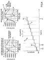
Figure 6 , the propagation of a band gap discontinuity across a PC designed with a band gap gradient modifies the Planckspectral distribution 70 of thermal electromagnetic radiation. More specifically, energy in the IR band near the peak of the Planck spectrum is captured and transferred to successively longer wavelength bands. This process not only shifts the primary emission wavelength but also reshapes the distribution by concentrating more thermal energy near the peak. As illustrated inFigure 6 , positioning the first band gap near (preferably below) the peak of the Planck distribution transfers a considerable amount of thermal energy to a longer wavelength λ1 so thatspectral distribution 72 has a narrow peak at λ1. At each successive step, the wavelength is shifted up, the intensity of the peak increases, the peak narrows and the tails are suppressed, producing a modifiedspectrum 74 at the last step. Although thermal energy is accumulated at each step, most of the energy is captured in the first step or couple of steps. Therefore it is very important to optimize the design and placement of the first PBG. In each successive step, the band gap is positioned further and further away from the peak of the underlying Planck distribution whose intensity diminishes rapidly at higher wavelengths. - As illustrated in
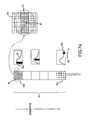
Figure 7a , an exemplary embodiment includes aPC 80 in which the lattice constant (spacing between scattering elements) is designed and spatially varied to create a piece-wise step continuousband gap gradient 82. Thefirst region 84a of the PC has a relatively small lattice constant that corresponds to aPBG 86a position near (preferably below) the peak of thePlanck distribution 88. Conversely, the Nth region 84n of the PC has a relatively large lattice constant that corresponds to aPBG 86n positioned considerably above the peak of thePlanck distribution 88. - The application of a mechanical pulse to the PC creates a
shock wave 90 that compresses the lattice constant 92 and shifts the dielectric constant thereby changing the refractive index. The change in refractive index outweighs the compression of the lattice constant so the net effect is to shift the band gap to a longer wavelength. Thermal electromagnetic radiation is trapped within the moving shock wave/PC interface as its wavelength is increased from the IR region to the THz region. As illustrated inFigure 7b , another embodiment includes aPC 93 in which the lattice constant (spacing between scattering elements 94) is designed and spatially varied to create a continuousband gap gradient 95. - The radiation core is suitably surrounded by or appended to a PC-based wave guiding and power-combining
structure 30 such that the radiated energy will be efficiently collected and directed to an output antenna(s) 32. The PC layer is suitably designed to have a band gap in the desired frequency band to achieve efficient coupling of radiation from the core to the output antenna(s). Various geometries and architectures can be used, depending on the application. - As shown in
Figure 8 , thermal electromagnetic radiation 100 (upshifted and concentrated) emitted by theradiation core 102 is coupled to aPC layer 104 in which a plurality ofdefect cavities 106 designed to resonate at the shifted peak are spaced across the PC orthogonal to the direction of propagation of theshockwave 108 to collect energy in a narrow band around the peak. Once the energy level has built up, every mth pulse, where m is determined by the Q of the cavities, causes thecavities 106 to couple and release energy to awaveguide 110 and out to anantenna 112 that emits abeam 114 of pulsed radiation. The source can be configured to either release some or all of the stored energy every mth pulse. Additional rows ofdefect cavities 106 can be used to capture any residual energy that was not captured by the first row. - As shown in
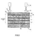
Figure 9 , rows ofdefect cavities 120 may be formed in respective regions 122 N, N-1, .... of the spatially varyingPC 124 in the radiation core itself and coupled torespective waveguides antennas electromagnetic radiation 133. In another alternate embodiment, an integratingcavity 134 can be coupled to the antennas to integrate the beam and provide continuous thermal electromagnetic radiation. - Besides the linear geometry discussed above, a
cylindrical configuration 150 as shown inFigure 10 is possible, with the band gap discontinuity propagating from aninner surface 152 to anouter surface 154 of the structure. In this case, the pulses can be generated by heating awire 156 positioned along the axis of the cylinder. The radiation is emitted from the entireouter surface 154 without resonant defect cavities to collect and redirect the radiation. Many other possible geometric arrangements exist for the band gap gradient including, for example, a spherical arrangement. - While several illustrative embodiments of the invention have been shown and described, numerous variations and alternate embodiments will occur to those skilled in the art. Such variations and alternate embodiments are contemplated, and can be made without departing from the scope of the invention as defined in the appended claims.
Claims (13)
- A method of modifying the Planck spectral distribution of thermal electromagnetic radiation emitted by a photonic crystal (PC), comprising:providing a PC being devided in N spatial regions having a first, second through N band gaps, whereby:intrinsic control parameters in an input spatial region of the PC create an input band gap near a primary emission wavelength of the spectral distribution; andintrinsic control parameters in an output spatial region of the PC create an output band gap shifted away from said primary emission wavelength; andapplying a pulse to the PC that acts on the control parameters to create a propagating band gap discontinuity (27) across the PC (14) to capture thermal energy in the input spatial region near the primary emission wavelength of the spectral distribution, shift the wavelength of the thermal energy, and transfer that energy to the output spatial region where the energy is emitted.
- The method of claim 1, further comprising heating (20) the PC to enhance the thermal electromagnetic radiation.
- The method of claim 1, wherein the control parameters are spatially varied across the PC to form a band gap gradient (18) such that the band gap changes along an axis of the PC, wherein said input spatial region and input band gap are at one end of the band gap gradient and said output spatial region and output band gap are at the other end of the band gap gradient.
- The method of claim 1, wherein a band gap gradient is formed by the input band gap in the input spatial region, an intermediate band gap in an intermediate spatial region and the output shifted band gap in the output region.
- The method of claim 4, wherein the band gap gradient is piece-wise step continuous (52a-52n).
- The method of claim 1, further comprising collecting the thermal electromagnetic radiation at the peak of the modified spectral distribution using a field of resonant defect cavities (106) and then collectively dumping the radiation stored therein into a waveguide (110).
- A radiation source, comprising:a photonic crystal (PC) (14) structure that emits internally generated thermal electromagnetic energy in a Planck spectral distribution, said PC being divided in N regions having a first, second through N band gaps, wherein spatially-varying intrinsic control parameters create an input band gap (52a) near a primary emission wavelength of the spectral distribution in an input spatial region and an output band gap shifted away from said primary emission wavelength in an output spatial region; anda source (32) that applies a pulse (24) to the PC to act on the intrinsic control parameters to propagate a band gap discontinuity (27) through the PC to capture thermal energy in the input spatial region near the primary emission wavelength of the spectral distribution, shift the wavelength of the thermal energy, and transfer that energy to the output spatial region where the energy is emitted to modify the Planck spectral distribution.
- The radiation source of claim 7, further comprising a heater (20) that heats the PC.
- The radiation source of claim 7, wherein the intrinsic control parameters vary spatially across the PC to form a band gap gradient such that that the band gap changes along an axis of the PC, wherein said input spatial region and input band gap are at one end of the band gap gradient and said output spatial region and output band gap are at the other end of the band gap gradient.
- The radiation source of claim 9, wherein the intrinsic control parameters vary spatially across the PC to create the input band gap (52a) in the input spatial region (50a) positioned near the peak of the Planck spectral distribution in the IR band, an intermediate shifted band gap (52b) in an intermediate spatial region (50b), and the output shifted band gap (52n) in the output spatial region (50n) positioned in another spectral band, said band gap discontinuity propagating through the PC capturing the thermal energy in each band of each region, shifting it in wavelength, and pushing the wavelength shifted radiation on to the next region.
- The radiation source of claim 7, further comprising a plurality of defect cavities (106) to collect the thermal energy and dump the energy into a waveguide (110) that directs it to an antenna (112).
- The radiation source of claim 11, wherein the defect cavities are local resonators tuned to the peak of the modified spectral distribution (74).
- The radiation source of claim 7, wherein:said spatially-varying intrinsic control parameters create an intermediate shifted band gap (52n) shifted between the input and output shifted band gaps in an intermediate spatial region (50n) between the input and output spatial regions, andthe pulse (24) is applied to the PC to act on the intrinsic control parameters to propagate the band gap discontinuity (27) through the PC to capture thermal energy in the input spatial region near the primary emission wavelength of the spectral distribution, shift the wavelength of the thermal energy to at least match the intermediate band gap, transfer the energy to the intermediate spatial region, shift the wavelength of the thermal region to at least match the output band gap and transfer that energy to the output spatial region where the wavelength-shifted energy is emitted to modify the Planck spectral distribution.
Priority Applications (1)
| Application Number | Priority Date | Filing Date | Title |
|---|---|---|---|
| PL06733618T PL1839328T3 (en) | 2005-01-06 | 2006-01-05 | Dynamic control of planck radiation in photonic crystals |
Applications Claiming Priority (2)
| Application Number | Priority Date | Filing Date | Title |
|---|---|---|---|
| US11/030,621 US7257333B2 (en) | 2005-01-06 | 2005-01-06 | Dynamic control of planck radiation in photonic crystals |
| PCT/US2006/000285 WO2006074282A1 (en) | 2005-01-06 | 2006-01-05 | Dynamic control of planck radiation in photonic crystals |
Publications (2)
| Publication Number | Publication Date |
|---|---|
| EP1839328A1 EP1839328A1 (en) | 2007-10-03 |
| EP1839328B1 true EP1839328B1 (en) | 2009-03-11 |
Family
ID=36481301
Family Applications (1)
| Application Number | Title | Priority Date | Filing Date |
|---|---|---|---|
| EP06733618A Expired - Lifetime EP1839328B1 (en) | 2005-01-06 | 2006-01-05 | Dynamic control of planck radiation in photonic crystals |
Country Status (9)
| Country | Link |
|---|---|
| US (1) | US7257333B2 (en) |
| EP (1) | EP1839328B1 (en) |
| JP (1) | JP2008527716A (en) |
| CN (1) | CN101099222B (en) |
| AT (1) | ATE425549T1 (en) |
| DE (1) | DE602006005608D1 (en) |
| PL (1) | PL1839328T3 (en) |
| RU (1) | RU2007129837A (en) |
| WO (1) | WO2006074282A1 (en) |
Families Citing this family (16)
| Publication number | Priority date | Publication date | Assignee | Title |
|---|---|---|---|---|
| US7421171B2 (en) * | 2006-06-23 | 2008-09-02 | Massachusetts Institute Of Technology | Efficient terahertz sources by optical rectification in photonic crystals and metamaterials exploiting tailored transverse dispersion relations |
| US7724420B2 (en) * | 2006-10-10 | 2010-05-25 | Raytheon Company | Frequency modulation structure and method utilizing frozen shockwave |
| US8023179B2 (en) * | 2007-03-15 | 2011-09-20 | Ofs Fitel Llc | Enhanced continuum generation in nonlinear bulk optic materials |
| WO2009036154A1 (en) * | 2007-09-13 | 2009-03-19 | Raytheon Company | Methods and systems for extracting energy from a heat source using photonic crystals with defect cavities |
| US8261557B2 (en) * | 2008-12-05 | 2012-09-11 | Raytheon Company | Heat transfer devices based on thermodynamic cycling of a photonic crystal with coupled resonant defect cavities |
| US8082844B1 (en) | 2009-05-28 | 2011-12-27 | Raytheon Company | Acoustic crystal explosives |
| US8026496B2 (en) * | 2009-07-02 | 2011-09-27 | Raytheon Company | Acoustic crystal sonoluminescent cavitation devices and IR/THz sources |
| US8477402B2 (en) | 2010-09-20 | 2013-07-02 | The Invention Science Fund I Llc | Photonic modulation of a photonic band gap |
| JP6860175B2 (en) * | 2016-02-29 | 2021-04-14 | 国立大学法人京都大学 | Two-dimensional photonic crystal surface emitting laser and its manufacturing method |
| KR102651032B1 (en) * | 2017-08-30 | 2024-03-25 | 바이오액시알 사스 | Super-resolution metrology method based on single distribution and deep learning |
| US11137432B1 (en) | 2020-03-16 | 2021-10-05 | Quantum Valley Ideas Laboratories | Photonic crystal receivers |
| WO2022087743A1 (en) | 2020-10-30 | 2022-05-05 | Quantum Valley Ideas Laboratories | Photonic crystal masers |
| US11619784B2 (en) * | 2021-07-29 | 2023-04-04 | Hewlett Packard Enterprise Development Lp | Optical device having photonic-crystal lattice structure for optical interconnects |
| US11402479B1 (en) | 2022-02-08 | 2022-08-02 | Quantum Valley Ideas Laboratories | Communicating information using photonic crystal transceivers |
| US11469566B1 (en) | 2022-02-08 | 2022-10-11 | Quantum Valley Ideas Laboratories | Generating electromagnetic radiation from a photonic crystal maser |
| US11533101B1 (en) | 2022-02-08 | 2022-12-20 | Quantum Valley Ideas Laboratories | Communicating information using photonic crystal masers |
Family Cites Families (8)
| Publication number | Priority date | Publication date | Assignee | Title |
|---|---|---|---|---|
| US6744552B2 (en) * | 1998-04-02 | 2004-06-01 | Michael Scalora | Photonic signal frequency up and down-conversion using a photonic band gap structure |
| US6778722B1 (en) * | 2001-04-25 | 2004-08-17 | Raytheon Company | Method and apparatus for switching optical signals with a photon band gap device |
| US6891993B2 (en) | 2001-06-11 | 2005-05-10 | The University Of Delaware | Multi-channel wavelength division multiplexing using photonic crystals |
| US6768256B1 (en) | 2001-08-27 | 2004-07-27 | Sandia Corporation | Photonic crystal light source |
| AU2003224944A1 (en) * | 2002-04-12 | 2003-10-27 | Massachusetts Institute Of Technology | Shock-wave modulation and control of electromagnetic radiation in a photonic crystal |
| US7079308B2 (en) | 2003-04-11 | 2006-07-18 | Massachusetts Institute Of Technology | Shock-wave modulation and control of electromagnetic radiation |
| US7116458B2 (en) | 2004-03-08 | 2006-10-03 | Massachusetts Institute Of Technology | Coherent generation, conversion, and modulation of electromagnetic radiation using shock waves or solitons propagating through polaritonic or excitonic materials |
| US7184641B2 (en) | 2004-05-07 | 2007-02-27 | Massachusetts Institute Of Technology | Surface-plasmon index guided (SPIG) waveguides and surface-plasmon effective index guided (SPEIG) waveguides |
-
2005
- 2005-01-06 US US11/030,621 patent/US7257333B2/en not_active Expired - Lifetime
-
2006
- 2006-01-05 PL PL06733618T patent/PL1839328T3/en unknown
- 2006-01-05 WO PCT/US2006/000285 patent/WO2006074282A1/en not_active Ceased
- 2006-01-05 RU RU2007129837/28A patent/RU2007129837A/en unknown
- 2006-01-05 DE DE602006005608T patent/DE602006005608D1/en not_active Expired - Lifetime
- 2006-01-05 JP JP2007550454A patent/JP2008527716A/en active Pending
- 2006-01-05 AT AT06733618T patent/ATE425549T1/en active
- 2006-01-05 CN CN2006800018225A patent/CN101099222B/en not_active Expired - Fee Related
- 2006-01-05 EP EP06733618A patent/EP1839328B1/en not_active Expired - Lifetime
Also Published As
| Publication number | Publication date |
|---|---|
| ATE425549T1 (en) | 2009-03-15 |
| EP1839328A1 (en) | 2007-10-03 |
| US20060147213A1 (en) | 2006-07-06 |
| US7257333B2 (en) | 2007-08-14 |
| CN101099222A (en) | 2008-01-02 |
| RU2007129837A (en) | 2009-02-20 |
| DE602006005608D1 (en) | 2009-04-23 |
| PL1839328T3 (en) | 2009-08-31 |
| JP2008527716A (en) | 2008-07-24 |
| WO2006074282A1 (en) | 2006-07-13 |
| CN101099222B (en) | 2010-04-14 |
Similar Documents
| Publication | Publication Date | Title |
|---|---|---|
| US7257333B2 (en) | Dynamic control of planck radiation in photonic crystals | |
| EP1878097B1 (en) | Smith-purcell radiation source using negative-index metamaterial (nim) | |
| US7078697B2 (en) | Thermally powered terahertz radiation source using photonic crystals | |
| US7825366B2 (en) | Methods and systems for extracting energy from a heat source using photonic crystals with defect cavities | |
| US8208191B2 (en) | Ultra-wide band slow light structure using plasmonic graded grating structures | |
| US8228129B2 (en) | Photonic crystal resonant defect cavities with nano-scale oscillators for generation of terahertz or infrared radiation | |
| US6832033B2 (en) | Hetero-structure photonic bandgap materials | |
| Chang et al. | Metasurface perfect absorber based on guided resonance of a photonic hypercrystal | |
| US7421171B2 (en) | Efficient terahertz sources by optical rectification in photonic crystals and metamaterials exploiting tailored transverse dispersion relations | |
| Nourmohammadi et al. | Ultra-wideband photonic hybrid plasmonic horn nanoantenna with SOI configuration | |
| Jafari et al. | An Innovative method for adjustable broadband THz to Mid-IR optical modulator using Graphene Gratings surface plasmon Fabry–Perot resonances with low insertion loss, high speed and modulation depth | |
| Lourtioz et al. | Toward controllable photonic crystals for centimeter-and millimeter-wave devices | |
| Tuz et al. | Enhancement of absorption bistability by trapping-light planar metamaterial | |
| Balaji et al. | Design and analysis of waveguide taper for photonic crystal demultiplexer | |
| Gennaro et al. | Nonlinear and ultrafast all-dielectric metasurfaces at the center for integrated nanotechnologies | |
| Matzen et al. | Systematic design of slow-light photonic waveguides | |
| CN118276228A (en) | Terahertz wave synthesized integrated spin waveguide chip | |
| US8369659B2 (en) | High-Q resonators assembly | |
| Srivastava et al. | Operating characteristics of an optical filter in metallic photonic bandgap materials | |
| JP2004279604A (en) | Wavelength converter | |
| Rajabalipanah et al. | A single metagrating metastructure for wave-based parallel analog computing | |
| Chen et al. | Terahertz localization and filtering effects in two-dimensional disordered scattering structures | |
| Paulillo | Circuit-tunable subwavelength terahertz devices | |
| Frezza et al. | Numerical investigation on the filtering behavior of 2-D PBGs with multiple periodic defects | |
| RU182626U1 (en) | DEVICE FOR RESONANT PHOTON CRYSTAL FOR CONTROLLING ELECTROMAGNETIC RADIATION PROPAGATION |
Legal Events
| Date | Code | Title | Description |
|---|---|---|---|
| PUAI | Public reference made under article 153(3) epc to a published international application that has entered the european phase |
Free format text: ORIGINAL CODE: 0009012 |
|
| 17P | Request for examination filed |
Effective date: 20070724 |
|
| AK | Designated contracting states |
Kind code of ref document: A1 Designated state(s): AT BE BG CH CY CZ DE DK EE ES FI FR GB GR HU IE IS IT LI LT LU LV MC NL PL PT RO SE SI SK TR |
|
| RIN1 | Information on inventor provided before grant (corrected) |
Inventor name: XIN, HAO Inventor name: OWENS, WILLIAM, R. Inventor name: BARKER, DELMAR, L. Inventor name: SHAH, NITESH, N. Inventor name: ROSENWALD, ROSS, D. |
|
| 17Q | First examination report despatched |
Effective date: 20071105 |
|
| DAX | Request for extension of the european patent (deleted) | ||
| GRAP | Despatch of communication of intention to grant a patent |
Free format text: ORIGINAL CODE: EPIDOSNIGR1 |
|
| GRAS | Grant fee paid |
Free format text: ORIGINAL CODE: EPIDOSNIGR3 |
|
| GRAA | (expected) grant |
Free format text: ORIGINAL CODE: 0009210 |
|
| AK | Designated contracting states |
Kind code of ref document: B1 Designated state(s): AT BE BG CH CY CZ DE DK EE ES FI FR GB GR HU IE IS IT LI LT LU LV MC NL PL PT RO SE SI SK TR |
|
| REG | Reference to a national code |
Ref country code: GB Ref legal event code: FG4D |
|
| REG | Reference to a national code |
Ref country code: CH Ref legal event code: EP |
|
| REG | Reference to a national code |
Ref country code: IE Ref legal event code: FG4D |
|
| REF | Corresponds to: |
Ref document number: 602006005608 Country of ref document: DE Date of ref document: 20090423 Kind code of ref document: P |
|
| PG25 | Lapsed in a contracting state [announced via postgrant information from national office to epo] |
Ref country code: SI Free format text: LAPSE BECAUSE OF FAILURE TO SUBMIT A TRANSLATION OF THE DESCRIPTION OR TO PAY THE FEE WITHIN THE PRESCRIBED TIME-LIMIT Effective date: 20090311 Ref country code: NL Free format text: LAPSE BECAUSE OF FAILURE TO SUBMIT A TRANSLATION OF THE DESCRIPTION OR TO PAY THE FEE WITHIN THE PRESCRIBED TIME-LIMIT Effective date: 20090311 Ref country code: LT Free format text: LAPSE BECAUSE OF FAILURE TO SUBMIT A TRANSLATION OF THE DESCRIPTION OR TO PAY THE FEE WITHIN THE PRESCRIBED TIME-LIMIT Effective date: 20090311 Ref country code: FI Free format text: LAPSE BECAUSE OF FAILURE TO SUBMIT A TRANSLATION OF THE DESCRIPTION OR TO PAY THE FEE WITHIN THE PRESCRIBED TIME-LIMIT Effective date: 20090311 |
|
| NLV1 | Nl: lapsed or annulled due to failure to fulfill the requirements of art. 29p and 29m of the patents act | ||
| PG25 | Lapsed in a contracting state [announced via postgrant information from national office to epo] |
Ref country code: SE Free format text: LAPSE BECAUSE OF FAILURE TO SUBMIT A TRANSLATION OF THE DESCRIPTION OR TO PAY THE FEE WITHIN THE PRESCRIBED TIME-LIMIT Effective date: 20090611 Ref country code: LV Free format text: LAPSE BECAUSE OF FAILURE TO SUBMIT A TRANSLATION OF THE DESCRIPTION OR TO PAY THE FEE WITHIN THE PRESCRIBED TIME-LIMIT Effective date: 20090311 |
|
| REG | Reference to a national code |
Ref country code: PL Ref legal event code: T3 |
|
| PG25 | Lapsed in a contracting state [announced via postgrant information from national office to epo] |
Ref country code: BE Free format text: LAPSE BECAUSE OF FAILURE TO SUBMIT A TRANSLATION OF THE DESCRIPTION OR TO PAY THE FEE WITHIN THE PRESCRIBED TIME-LIMIT Effective date: 20090311 |
|
| PG25 | Lapsed in a contracting state [announced via postgrant information from national office to epo] |
Ref country code: PT Free format text: LAPSE BECAUSE OF FAILURE TO SUBMIT A TRANSLATION OF THE DESCRIPTION OR TO PAY THE FEE WITHIN THE PRESCRIBED TIME-LIMIT Effective date: 20090824 Ref country code: ES Free format text: LAPSE BECAUSE OF FAILURE TO SUBMIT A TRANSLATION OF THE DESCRIPTION OR TO PAY THE FEE WITHIN THE PRESCRIBED TIME-LIMIT Effective date: 20090622 Ref country code: EE Free format text: LAPSE BECAUSE OF FAILURE TO SUBMIT A TRANSLATION OF THE DESCRIPTION OR TO PAY THE FEE WITHIN THE PRESCRIBED TIME-LIMIT Effective date: 20090311 Ref country code: CZ Free format text: LAPSE BECAUSE OF FAILURE TO SUBMIT A TRANSLATION OF THE DESCRIPTION OR TO PAY THE FEE WITHIN THE PRESCRIBED TIME-LIMIT Effective date: 20090311 |
|
| PG25 | Lapsed in a contracting state [announced via postgrant information from national office to epo] |
Ref country code: SK Free format text: LAPSE BECAUSE OF FAILURE TO SUBMIT A TRANSLATION OF THE DESCRIPTION OR TO PAY THE FEE WITHIN THE PRESCRIBED TIME-LIMIT Effective date: 20090311 Ref country code: RO Free format text: LAPSE BECAUSE OF FAILURE TO SUBMIT A TRANSLATION OF THE DESCRIPTION OR TO PAY THE FEE WITHIN THE PRESCRIBED TIME-LIMIT Effective date: 20090311 Ref country code: IS Free format text: LAPSE BECAUSE OF FAILURE TO SUBMIT A TRANSLATION OF THE DESCRIPTION OR TO PAY THE FEE WITHIN THE PRESCRIBED TIME-LIMIT Effective date: 20090711 |
|
| PLBE | No opposition filed within time limit |
Free format text: ORIGINAL CODE: 0009261 |
|
| STAA | Information on the status of an ep patent application or granted ep patent |
Free format text: STATUS: NO OPPOSITION FILED WITHIN TIME LIMIT |
|
| PG25 | Lapsed in a contracting state [announced via postgrant information from national office to epo] |
Ref country code: DK Free format text: LAPSE BECAUSE OF FAILURE TO SUBMIT A TRANSLATION OF THE DESCRIPTION OR TO PAY THE FEE WITHIN THE PRESCRIBED TIME-LIMIT Effective date: 20090311 Ref country code: BG Free format text: LAPSE BECAUSE OF FAILURE TO SUBMIT A TRANSLATION OF THE DESCRIPTION OR TO PAY THE FEE WITHIN THE PRESCRIBED TIME-LIMIT Effective date: 20090611 |
|
| 26N | No opposition filed |
Effective date: 20091214 |
|
| PG25 | Lapsed in a contracting state [announced via postgrant information from national office to epo] |
Ref country code: MC Free format text: LAPSE BECAUSE OF NON-PAYMENT OF DUE FEES Effective date: 20100131 |
|
| REG | Reference to a national code |
Ref country code: CH Ref legal event code: PL |
|
| REG | Reference to a national code |
Ref country code: IE Ref legal event code: MM4A |
|
| PG25 | Lapsed in a contracting state [announced via postgrant information from national office to epo] |
Ref country code: LI Free format text: LAPSE BECAUSE OF NON-PAYMENT OF DUE FEES Effective date: 20100131 Ref country code: GR Free format text: LAPSE BECAUSE OF FAILURE TO SUBMIT A TRANSLATION OF THE DESCRIPTION OR TO PAY THE FEE WITHIN THE PRESCRIBED TIME-LIMIT Effective date: 20090612 Ref country code: CH Free format text: LAPSE BECAUSE OF NON-PAYMENT OF DUE FEES Effective date: 20100131 |
|
| PG25 | Lapsed in a contracting state [announced via postgrant information from national office to epo] |
Ref country code: IE Free format text: LAPSE BECAUSE OF NON-PAYMENT OF DUE FEES Effective date: 20100105 |
|
| PG25 | Lapsed in a contracting state [announced via postgrant information from national office to epo] |
Ref country code: CY Free format text: LAPSE BECAUSE OF FAILURE TO SUBMIT A TRANSLATION OF THE DESCRIPTION OR TO PAY THE FEE WITHIN THE PRESCRIBED TIME-LIMIT Effective date: 20090311 |
|
| PG25 | Lapsed in a contracting state [announced via postgrant information from national office to epo] |
Ref country code: HU Free format text: LAPSE BECAUSE OF FAILURE TO SUBMIT A TRANSLATION OF THE DESCRIPTION OR TO PAY THE FEE WITHIN THE PRESCRIBED TIME-LIMIT Effective date: 20090912 Ref country code: LU Free format text: LAPSE BECAUSE OF NON-PAYMENT OF DUE FEES Effective date: 20100105 |
|
| PG25 | Lapsed in a contracting state [announced via postgrant information from national office to epo] |
Ref country code: TR Free format text: LAPSE BECAUSE OF FAILURE TO SUBMIT A TRANSLATION OF THE DESCRIPTION OR TO PAY THE FEE WITHIN THE PRESCRIBED TIME-LIMIT Effective date: 20090311 |
|
| REG | Reference to a national code |
Ref country code: FR Ref legal event code: PLFP Year of fee payment: 11 |
|
| REG | Reference to a national code |
Ref country code: FR Ref legal event code: PLFP Year of fee payment: 12 |
|
| REG | Reference to a national code |
Ref country code: FR Ref legal event code: PLFP Year of fee payment: 13 |
|
| PGFP | Annual fee paid to national office [announced via postgrant information from national office to epo] |
Ref country code: DE Payment date: 20191224 Year of fee payment: 15 Ref country code: AT Payment date: 20191227 Year of fee payment: 15 Ref country code: GB Payment date: 20191230 Year of fee payment: 15 |
|
| PGFP | Annual fee paid to national office [announced via postgrant information from national office to epo] |
Ref country code: FR Payment date: 20201210 Year of fee payment: 16 |
|
| PGFP | Annual fee paid to national office [announced via postgrant information from national office to epo] |
Ref country code: PL Payment date: 20201214 Year of fee payment: 16 |
|
| PGFP | Annual fee paid to national office [announced via postgrant information from national office to epo] |
Ref country code: IT Payment date: 20201211 Year of fee payment: 16 |
|
| REG | Reference to a national code |
Ref country code: DE Ref legal event code: R119 Ref document number: 602006005608 Country of ref document: DE |
|
| REG | Reference to a national code |
Ref country code: AT Ref legal event code: MM01 Ref document number: 425549 Country of ref document: AT Kind code of ref document: T Effective date: 20210105 |
|
| GBPC | Gb: european patent ceased through non-payment of renewal fee |
Effective date: 20210105 |
|
| PG25 | Lapsed in a contracting state [announced via postgrant information from national office to epo] |
Ref country code: AT Free format text: LAPSE BECAUSE OF NON-PAYMENT OF DUE FEES Effective date: 20210105 |
|
| PG25 | Lapsed in a contracting state [announced via postgrant information from national office to epo] |
Ref country code: DE Free format text: LAPSE BECAUSE OF NON-PAYMENT OF DUE FEES Effective date: 20210803 Ref country code: GB Free format text: LAPSE BECAUSE OF NON-PAYMENT OF DUE FEES Effective date: 20210105 |
|
| PG25 | Lapsed in a contracting state [announced via postgrant information from national office to epo] |
Ref country code: FR Free format text: LAPSE BECAUSE OF NON-PAYMENT OF DUE FEES Effective date: 20220131 |
|
| PG25 | Lapsed in a contracting state [announced via postgrant information from national office to epo] |
Ref country code: IT Free format text: LAPSE BECAUSE OF NON-PAYMENT OF DUE FEES Effective date: 20220105 |
|
| PG25 | Lapsed in a contracting state [announced via postgrant information from national office to epo] |
Ref country code: PL Free format text: LAPSE BECAUSE OF NON-PAYMENT OF DUE FEES Effective date: 20220105 |