EP1837915A2 - Semiconductors - Google Patents
Semiconductors Download PDFInfo
- Publication number
- EP1837915A2 EP1837915A2 EP07104449A EP07104449A EP1837915A2 EP 1837915 A2 EP1837915 A2 EP 1837915A2 EP 07104449 A EP07104449 A EP 07104449A EP 07104449 A EP07104449 A EP 07104449A EP 1837915 A2 EP1837915 A2 EP 1837915A2
- Authority
- EP
- European Patent Office
- Prior art keywords
- semiconductor substrate
- forming
- semiconductor region
- hetero
- trench
- Prior art date
- Legal status (The legal status is an assumption and is not a legal conclusion. Google has not performed a legal analysis and makes no representation as to the accuracy of the status listed.)
- Granted
Links
Images





Classifications
-
- H—ELECTRICITY
- H10—SEMICONDUCTOR DEVICES; ELECTRIC SOLID-STATE DEVICES NOT OTHERWISE PROVIDED FOR
- H10D—INORGANIC ELECTRIC SEMICONDUCTOR DEVICES
- H10D12/00—Bipolar devices controlled by the field effect, e.g. insulated-gate bipolar transistors [IGBT]
- H10D12/01—Manufacture or treatment
- H10D12/031—Manufacture or treatment of IGBTs
-
- H—ELECTRICITY
- H10—SEMICONDUCTOR DEVICES; ELECTRIC SOLID-STATE DEVICES NOT OTHERWISE PROVIDED FOR
- H10D—INORGANIC ELECTRIC SEMICONDUCTOR DEVICES
- H10D30/00—Field-effect transistors [FET]
- H10D30/60—Insulated-gate field-effect transistors [IGFET]
- H10D30/63—Vertical IGFETs
- H10D30/635—Vertical IGFETs having no inversion channels, e.g. vertical accumulation channel FETs [ACCUFET] or normally-on vertical IGFETs
-
- H—ELECTRICITY
- H10—SEMICONDUCTOR DEVICES; ELECTRIC SOLID-STATE DEVICES NOT OTHERWISE PROVIDED FOR
- H10D—INORGANIC ELECTRIC SEMICONDUCTOR DEVICES
- H10D30/00—Field-effect transistors [FET]
- H10D30/60—Insulated-gate field-effect transistors [IGFET]
- H10D30/64—Double-diffused metal-oxide semiconductor [DMOS] FETs
- H10D30/66—Vertical DMOS [VDMOS] FETs
- H10D30/668—Vertical DMOS [VDMOS] FETs having trench gate electrodes, e.g. UMOS transistors
-
- H—ELECTRICITY
- H10—SEMICONDUCTOR DEVICES; ELECTRIC SOLID-STATE DEVICES NOT OTHERWISE PROVIDED FOR
- H10D—INORGANIC ELECTRIC SEMICONDUCTOR DEVICES
- H10D62/00—Semiconductor bodies, or regions thereof, of devices having potential barriers
- H10D62/80—Semiconductor bodies, or regions thereof, of devices having potential barriers characterised by the materials
- H10D62/82—Heterojunctions
-
- H—ELECTRICITY
- H10—SEMICONDUCTOR DEVICES; ELECTRIC SOLID-STATE DEVICES NOT OTHERWISE PROVIDED FOR
- H10D—INORGANIC ELECTRIC SEMICONDUCTOR DEVICES
- H10D62/00—Semiconductor bodies, or regions thereof, of devices having potential barriers
- H10D62/80—Semiconductor bodies, or regions thereof, of devices having potential barriers characterised by the materials
- H10D62/83—Semiconductor bodies, or regions thereof, of devices having potential barriers characterised by the materials being Group IV materials, e.g. B-doped Si or undoped Ge
- H10D62/832—Semiconductor bodies, or regions thereof, of devices having potential barriers characterised by the materials being Group IV materials, e.g. B-doped Si or undoped Ge being Group IV materials comprising two or more elements, e.g. SiGe
- H10D62/8325—Silicon carbide
-
- H—ELECTRICITY
- H10—SEMICONDUCTOR DEVICES; ELECTRIC SOLID-STATE DEVICES NOT OTHERWISE PROVIDED FOR
- H10D—INORGANIC ELECTRIC SEMICONDUCTOR DEVICES
- H10D64/00—Electrodes of devices having potential barriers
- H10D64/20—Electrodes characterised by their shapes, relative sizes or dispositions
- H10D64/27—Electrodes not carrying the current to be rectified, amplified, oscillated or switched, e.g. gates
- H10D64/311—Gate electrodes for field-effect devices
- H10D64/411—Gate electrodes for field-effect devices for FETs
- H10D64/511—Gate electrodes for field-effect devices for FETs for IGFETs
- H10D64/512—Disposition of the gate electrodes, e.g. buried gates
- H10D64/513—Disposition of the gate electrodes, e.g. buried gates within recesses in the substrate, e.g. trench gates, groove gates or buried gates
-
- H—ELECTRICITY
- H10—SEMICONDUCTOR DEVICES; ELECTRIC SOLID-STATE DEVICES NOT OTHERWISE PROVIDED FOR
- H10P—GENERIC PROCESSES OR APPARATUS FOR THE MANUFACTURE OR TREATMENT OF DEVICES COVERED BY CLASS H10
- H10P50/00—Etching of wafers, substrates or parts of devices
- H10P50/71—Etching of wafers, substrates or parts of devices using masks for conductive or resistive materials
-
- H—ELECTRICITY
- H10—SEMICONDUCTOR DEVICES; ELECTRIC SOLID-STATE DEVICES NOT OTHERWISE PROVIDED FOR
- H10P—GENERIC PROCESSES OR APPARATUS FOR THE MANUFACTURE OR TREATMENT OF DEVICES COVERED BY CLASS H10
- H10P76/00—Manufacture or treatment of masks on semiconductor bodies, e.g. by lithography or photolithography
- H10P76/20—Manufacture or treatment of masks on semiconductor bodies, e.g. by lithography or photolithography of masks comprising organic materials
- H10P76/204—Manufacture or treatment of masks on semiconductor bodies, e.g. by lithography or photolithography of masks comprising organic materials of organic photoresist masks
Definitions
- the N - -type polycrystal silicon region is connected to a source electrode. Further, a drain electrode is formed at an underside of the N + -type silicon carbide substrate.
- a further example of a method of manufacturing a semiconductor device comprises depositing a hetero semiconductor region on a first conductive-type semiconductor substrate, wherein the hetero semiconductor region forms a heterojunction with the semiconductor substrate, and forming a trench wherein a bottom portion of the trench extends to the semiconductor substrate and a thickness of a portion of the hetero semiconductor region around the trench is smaller than a thickness of other portions of the hetero semiconductor region, wherein forming the trench includes selectively removing the semiconductor substrate and the hetero semiconductor region by an isotropic etching.
- a sacrificial oxide film 22 is formed by thermally oxidizing an exposed portion of the polycrystal silicon, i.e., the hetero semiconductor region 3.
- a surface of the drain region 2 containing SiC is also oxidized.
- the amount of the drain region 2 (containing SiC) being oxidized becomes smaller than that of the hetero semiconductor region 3 containing polycrystal silicon. This is shown in Fig. 2d.
- the exposed portion may be removed through wet etching, which sets a certain selection ratio between polycristal silicon and SiC.
- wet etching sets a certain selection ratio between polycristal silicon and SiC.
- the configuration of Fig. 1 can be obtained (i.e., the driving point 6 is spaced apart from the side wall of the trench).
- it is possible to achieve this configuration by forming a resist material for the mask material used in the process shown in Fig. 2c. Then, the same wet etching can be performed after conducting a reduction process on the resist material through baking or UV irradiating.
- the gate electrode 7 is formed in the trench, which is formed in the inner portion of the drain region 2. Accordingly, when the device is in a non-conduction state, the voltage of the gate electrode 7 positioned at a certain depth in the drain region 2 is fixed to 0V. Further, it is possible to shield an electrical field formed by high voltage applied to the drain electrode 10 at a deeper position. Therefore, the effect of lessening an electrical field around the driving point 6 is increased such that a leak current can be reduced when the device is in an off state.
- Fig. 3 illustrates the configuration of a semiconductor device constructed in accordance with a second embodiment of the invention.
- the trench is formed in the inner portion of the drain region 2 as shown in Fig. 2c.
- the second embodiment shown in Fig. 3 has a configuration similar to the first embodiment except that a bottom portion 11 of the trench (a bottom portion of a dry etching surface) made by dry etching is positioned at a junction interface of the hetero semiconductor region 3 and the drain region 2.
- the effect of reducing a leak current when the device is in a non-conduction state can be obtained in addition to the effects achieved by the second embodiment. Further, a device having a high pressure-resistance can be obtained with low impedance.
- a photomask 32 is formed on the resist 31 as shown in Fig. 8b.
- the resist 31 is selectively removed and patterned through etching using the photomask 32.
- a semiconductor device that has the characteristics of the first embodiment can be easily manufactured. Further, by employing the above manufacturing method, it is possible to lightly perform a sacrificial oxidation on the hetero semiconductor region 3 in a longitudinal direction when forming the driving point 6 in a position spaced apart from the etching surface by about thousands of A. Therefore, the amount of the sacrificial oxidization can be restrained, and a load of the manufacturing process can be reduced. Furthermore, the adverse effect caused by heavy sacrificial oxidization can be reduced.
- a photomask 32 is next formed on the resist 31.
- the resist 31 is selectively removed and patterned through etching by using the photomask 32 as shown in Fig. 10b.
- dry etching i.e., anisotropic etching
- anisotropic etching is performed to selectively remove the hetero semiconductor region 3 and the drain region 2 by using the resist 31, the edge portion 31a of which has a taper form, as a mask.
- a trench 35 is formed such that a bottom portion thereof extends to the drain region 2.
- each edge portion 31a of the resist 31 having a taper form is more rapidly etched than the other portions of the resist 31 through anisotropic etching.
- the underlying hetero semiconductor region 3 is etched.
- a portion of the hetero semiconductor region 3, the thickness of which becomes gradually thinner, is formed around the trench 35 as shown in Fig. 10d.
- the thickness of the thinner portion of the hetero semiconductor region 3 is about thousands of A. Further, a length of the hetero semiconductor region 3, the thickness of which becomes thinner, is about thousands of A in the lateral direction from an end of the trench 35.
- the semiconductor device shown in Fig. 1 is obtained through the processes shown in Figs. 2f to 2k and Figs. 8e and 8f, which have been explained above in relation to the first and seventh embodiments.
- impurities are introduced into the hetero semiconductor region 3 of a polycrystal silicon by using, for example, a mechanism such as ion injection. This is done so that the hetero semiconductor region 3 becomes N + -type.
- impurities include As (arsenic), P (phosphorous) and the like.
- a resist 31 corresponding to a mask material is applied on the hetero semiconductor region 3. The resulting structure is shown in Fig. 11a.
Landscapes
- Electrodes Of Semiconductors (AREA)
- Insulated Gate Type Field-Effect Transistor (AREA)
- Thin Film Transistor (AREA)
Abstract
Description
- The present invention generally relates to semiconductors and particularly, but not exclusively, to a semiconductor device having a field effect transistor with a heterojunction and a method of manufacturing the same. Aspects of the invention relate to a device and to a method.
-
Japanese Laid-Open Patent Publication No. 2003-318398 - The N--type polycrystal silicon region is connected to a source electrode. Further, a drain electrode is formed at an underside of the N+-type silicon carbide substrate.
- Such a semiconductor device functions as a switch of a field effect transistor by controlling an electrical potential of the gate electrode when the source electrode is grounded to apply a predetermined positive electrical potential to the drain electrode. That is, when the gate electrode is grounded, a reverse bias is applied to the heterojunction of the N'-type polycrystal silicon region and the epitaxial region such that the current does not flow between the drain and source electrodes. However, when a predetermined positive voltage is applied to the gate electrode, a gate electrical field affects the heterojunction interface of the N--type polycrystal silicon region and the epitaxial region. Further, the thickness of an energy barrier formed by the heterojunction surface of the gate oxide film interface becomes thinner. As such, the current flows between the drain electrode and the source electrode.
- In addition, the above semiconductor device uses the heterojunction portion as a control channel for blocking and conducting the current. Also, the length of the channel depends on the thickness of a hetero barrier, thereby obtaining a low resistance conduction characteristic. As such, a lower resistance conduction can be obtained as the intensity of the gate electrical field becomes greater in the heterojunction interface of the N--type polycrystal silicon region and the epitaxial region where the gate electrode is adjoined using the gate insulating film.
- In the above semiconductor device, the hetero semiconductor region is etched by using a dry etching method and the like. Further, the gate insulating film is formed at a side surface thereof to form a driving point where the hetero semiconductor region, the semiconductor substrate and the gate insulating film are adjoined. However, damage caused by etching remains on the driving point to thereby hinder the driving power of the transistor. This makes it very difficult to reduce impedance in a switching element of the transistor.
- It is an aim of the present invention to address this issue and to improve upon known technology. Other aims and advantages of the invention will become apparent from the following description, claims and drawings.
- Aspects of the invention therefore provide a device and a method as claimed in the appended claims.
- According to another aspect of the invention there is provided a semiconductor device, comprising a semiconductor substrate of a first conductive-type, the semiconductor substrate having a trench formed therein, a heterojunction forming portion adjoined to a main surface of the semiconductor substrate and forming a heterojunction with the semiconductor substrate, a gate electrode disposed adjacent to a junction end of the heterojunction forming portion and the semiconductor substrate using a gate insulating film, a source electrode connected to the heterojunction forming portion, a drain electrode connected to the semiconductor substrate and a driving point of the semiconductor substrate where the gate insulating film, the hetero semiconductor region and the semiconductor substrate are adjoined is at a position spaced apart from a side wall of the trench.
- In an embodiment, the heterojunction forming portion around the driving point is of the first conductive-type.
- In an embodiment, the semiconductor substrate comprises at least one of a silicon carbide, a gallium nitride and a diamond.
- In an embodiment, the heterojunction forming portion comprises at least one of a single crystal silicon, a polycrystal silicon, an amorphous silicon, a single silicon germanium, a polycrystal silicon germanium and an amorphous silicon germanium.
- According to yet another aspect of the invention there is provided a method of manufacturing a semiconductor device, comprising depositing a hetero semiconductor region on a semiconductor substrate of a first conductive-type, wherein the hetero semiconductor region forms a heterojunction with the semiconductor substrate, forming a trench by selectively removing portions of the semiconductor substrate and the hetero semiconductor region by a dry etching, forming a sacrificial oxide film by thermally oxidizing the semiconductor substrate and the hetero semiconductor region forming at least a side wall of the trench, removing the sacrificial oxide film, forming a gate insulating film on an exposed surface of the semiconductor substrate and the hetero semiconductor region including an inner surface of the trench after removing the sacrificial oxide film, forming a gate electrode adjacent to a junction end of the semiconductor substrate and the hetero semiconductor region using the gate insulating film, forming a source electrode connected to the hetero semiconductor region and forming a drain electrode connected to the semiconductor substrate; and wherein a device driving point where the gate insulating film, the hetero semiconductor region and the semiconductor substrate are adjoined is at a position spaced apart from a side wall of the trench.
- In an embodiment, forming the source electrode connected to the hetero semiconductor region occurs after forming the gate electrode. Forming the drain electrode connected to the semiconductor substrate may occur after forming the source electrode.
- According to a further aspect of the invention there is provided a method of manufacturing a semiconductor device, comprising depositing a hetero semiconductor region on a semiconductor substrate of a first conductive-type, wherein the hetero semiconductor region forms a heterojunction with the semiconductor substrate, forming a trench by selectively removing the semiconductor substrate and the hetero semiconductor region by a dry etching, selectively etching the semiconductor substrate and the hetero semiconductor region by a wet etching, wherein the wet etching has different selecting ratios for the semiconductor substrate and the hetero semiconductor region, forming a gate insulating film in the semiconductor substrate and the hetero semiconductor region including an inner surface of the trench after selectively etching the semiconductor substrate and the hetero semiconductor region by the wet etching, forming a gate electrode adjacent to a junction end of the semiconductor substrate and the hetero semiconductor region using the gate insulating film, forming a source electrode connected to the hetero semiconductor region and forming a drain electrode connected to the semiconductor substrate; and wherein a driving point of the semiconductor device where the gate insulating film, the hetero semiconductor region and the semiconductor substrate are adjoined is at a position spaced apart from a side wall of the trench.
- In an embodiment, forming the trench by selectively removing the semiconductor substrate and the hetero semiconductor region by the dry etching includes selectively removing the semiconductor substrate and the hetero semiconductor region using a mask material. The method may comprise reducing the mask material used in selectively removing the semiconductor substrate and the hetero semiconductor region prior to selectively etching the semiconductor substrate and the hetero semiconductor region by the wet etching.
- According to a still further aspect of the invention there is provided a method of manufacturing a semiconductor device, comprising depositing a hetero semiconductor region on a first conductive-type semiconductor substrate, wherein the hetero semiconductor region forms a heterojunction with the semiconductor substrate, forming a trench by selectively removing the hetero semiconductor region by a dry etching, wherein a bottom surface of the trench is a junction interface of the semiconductor substrate and the hetero semiconductor region, forming a sacrificial oxide film by thermally oxidizing the semiconductor substrate and the hetero semiconductor region forming at least an inner portion of the trench, removing the sacrificial oxide film, forming a gate insulating film on the semiconductor substrate and the hetero semiconductor region including the inner surface of the trench after removing the sacrificial oxide film, forming a gate electrode adjacent to a junction end of the semiconductor substrate and the hetero semiconductor region using the gate insulating film, forming a source electrode connected to the hetero semiconductor region and forming a drain electrode connected to the semiconductor substrate; and wherein a driving point of the semiconductor device where the gate insulating film, the hetero semiconductor region and the semiconductor substrate are adjoined is formed at a position spaced apart from a side wall of the trench before forming the sacrificial oxide film.
- According to another aspect of the invention there is provided a method of manufacturing a semiconductor device, comprising depositing a hetero semiconductor region on a first conductive-type semiconductor substrate, wherein the hetero semiconductor region forms a heterojunction with the semiconductor substrate, forming a trench wherein a bottom portion of the trench extends to the semiconductor substrate and a thickness of a portion of the hetero semiconductor region around the trench is smaller than a thickness of other portions of the hetero semiconductor region, wherein forming the trench includes selectively removing the semiconductor substrate and the hetero semiconductor region by an isotropic etching, forming a sacrificial oxide film by thermally oxidizing at least the hetero semiconductor region after forming the trench, selectively removing the portion of the hetero semiconductor region around the trench smaller that the thickness of the other portions by removing the sacrificial oxide film, forming the gate insulating film on the semiconductor substrate and the hetero semiconductor region including an inner surface of the trench after removing the sacrificial oxide film, forming a gate electrode adjacent to a junction end of the semiconductor substrate and the hetero semiconductor region using the gate insulating film, forming a source electrode connected to the hetero semiconductor region and forming a drain electrode connected to the semiconductor substrate; and wherein a driving point of the semiconductor device where the gate insulating film, the hetero semiconductor region and the semiconductor substrate are adjoined is at a position spaced apart from a side wall of the trench.
- Forming the trench may comprise performing an anisotropic etching by using a mask pattern used in the isotropic etching after performing the isotropic etching and selectively removing the semiconductor substrate and the hetero semiconductor region after performing the anisotropic etching and before forming the sacrificial oxide film.
- Forming the trench may comprise selectively removing, through an anisotropic etching, an edge portion of a mask pattern used by the isotropic etching and selectively removing the semiconductor substrate and the hetero semiconductor region using the mask pattern after the anisotropic etching and before forming the sacrificial oxide film.
- In an embodiment, the mask pattern includes a resist material and an edge portion thereof is formed in a taper form by an exposure or development process.
- In an embodiment, the isotropic etching is a wet etching or a chemical dry etching.
- In an embodiment, the semiconductor substrate comprises at least one of a silicon carbide, a gallium nitride and a diamond, and wherein the hetero semiconductor region comprises at least one of a single crystal silicon, a polycrystal silicon, an amorphous silicon, a single silicon germanium, a polycrystal silicon germanium and an amorphous silicon germanium.
- Embodiments of the invention may provide a semiconductor device having a heterojunction and being adapted to reduce impedance, as well as a method of manufacturing the same. For example, embodiments of the invention may provide a semiconductor device that include a first conductive-type semiconductor substrate, a hetero semiconductor region adjoined to a main surface of the semiconductor substrate to form a heterojunction with the semiconductor substrate, a gate electrode disposed adjacent to a junction end of the hetero semiconductor region and the semiconductor substrate using a gate insulating film, a source electrode connected to the hetero semiconductor region and a drain electrode connected to the semiconductor substrate. In these semiconductor devices, a trench is formed within the semiconductor substrate. Further, a driving point of the semiconductor device (where the gate insulating film, the hetero semiconductor region and the semiconductor substrate are adjoined) is formed and located apart from a side wall of the trench.
- According embodiments described herein, the driving point of the semiconductor device is formed at a region unaffected by the etching damage caused when forming the trench. Therefore, the driving power of the semiconductor device can be improved to thereby reduce impedance.
- For example, a semiconductor device may comprise a semiconductor substrate of a first conductive-type, the semiconductor substrate having a trench formed therein, and a heterojunction forming portion adjoined to a main surface of the semiconductor substrate and forming a heterojunction with the semiconductor substrate. A gate electrode is disposed adjacent to a junction end of the heterojunction forming portion and the semiconductor substrate using a gate insulating film, a source electrode is connected to the heterojunction forming portion, and a drain electrode is connected to the semiconductor substrate. A driving point of the semiconductor substrate where the gate insulating film, the hetero semiconductor region and the semiconductor substrate are adjoined is at a position spaced apart from a side wall of the trench.
- One example of a method of manufacturing a semiconductor device comprises depositing a hetero semiconductor region on a semiconductor substrate of a first conductive-type, wherein the hetero semiconductor region forms a heterojunction with the semiconductor substrate, forming a trench by selectively removing portions of the semiconductor substrate and the hetero semiconductor region by a dry etching, forming a sacrificial oxide film by thermally oxidizing the semiconductor substrate and the hetero semiconductor region forming at least a side wall of the trench, removing the sacrificial oxide film, forming a gate insulating film on an exposed surface of the semiconductor substrate and the hetero semiconductor region including an inner surface of the trench after removing the sacrificial oxide film, forming a gate electrode adjacent to a junction end of the semiconductor substrate and the hetero semiconductor region using the gate insulating film, forming a source electrode connected to the hetero semiconductor region and forming a drain electrode connected to the semiconductor substrate. A device driving point where the gate insulating film, the hetero semiconductor region and the semiconductor substrate are adjoined is at a position spaced apart from a side wall of the trench.
- Another example of a method of manufacturing a semiconductor device comprises depositing a hetero semiconductor region on a semiconductor substrate of a first conductive-type, wherein the hetero semiconductor region forms a heterojunction with the semiconductor substrate, and forming a trench by selectively removing the semiconductor substrate and the hetero semiconductor region by a dry etching. Then, the method includes selectively etching the semiconductor substrate and the hetero semiconductor region by a wet etching, wherein the wet etching has different selecting ratios for the semiconductor substrate and the hetero semiconductor region. The method further includes forming a gate insulating film in the semiconductor substrate and the hetero semiconductor region including an inner surface of the trench after selectively etching the semiconductor substrate and the hetero semiconductor region by the wet etching, forming a gate electrode adjacent to a junction end of the semiconductor substrate and the hetero semiconductor region using the gate insulating film, forming a source electrode connected to the hetero semiconductor region and forming a drain electrode connected to the semiconductor substrate. A driving point of the semiconductor device where the gate insulating film, the hetero semiconductor region and the semiconductor substrate are adjoined is at a position spaced apart from a side wall of the trench.
- Yet another example of a method of manufacturing a semiconductor device comprises depositing a hetero semiconductor region on a first conductive-type semiconductor substrate, wherein the hetero semiconductor region forms a heterojunction with the semiconductor substrate, forming a trench by selectively removing the hetero semiconductor region by a dry etching, wherein a bottom surface of the trench is a junction interface of the semiconductor substrate and the hetero semiconductor region, forming a sacrificial oxide film by thermally oxidizing the semiconductor substrate and the hetero semiconductor region forming at least an inner portion of the trench, removing the sacrificial oxide film, forming a gate insulating film on the semiconductor substrate and the hetero semiconductor region including the inner surface of the trench after removing the sacrificial oxide film, forming a gate electrode adjacent to a junction end of the semiconductor substrate and the hetero semiconductor region using the gate insulating film, forming a source electrode connected to the hetero semiconductor region and forming a drain electrode connected to the semiconductor substrate. A driving point of the semiconductor device where the gate insulating film, the hetero semiconductor region and the semiconductor substrate are adjoined is formed at a position spaced apart from a side wall of the trench before forming the sacrificial oxide film.
- A further example of a method of manufacturing a semiconductor device comprises depositing a hetero semiconductor region on a first conductive-type semiconductor substrate, wherein the hetero semiconductor region forms a heterojunction with the semiconductor substrate, and forming a trench wherein a bottom portion of the trench extends to the semiconductor substrate and a thickness of a portion of the hetero semiconductor region around the trench is smaller than a thickness of other portions of the hetero semiconductor region, wherein forming the trench includes selectively removing the semiconductor substrate and the hetero semiconductor region by an isotropic etching. The method further includes forming a sacrificial oxide film by thermally oxidizing at least the hetero semiconductor region after forming the trench, selectively removing the portion of the hetero semiconductor region around the trench smaller that the thickness of the other portions by removing the sacrificial oxide film, forming the gate insulating film on the semiconductor substrate and the hetero semiconductor region including an inner surface of the trench after removing the sacrificial oxide film, forming a gate electrode adjacent to a junction end of the semiconductor substrate and the hetero semiconductor region using the gate insulating film, forming a source electrode connected to the hetero semiconductor region and forming a drain electrode connected to the semiconductor substrate. A driving point of the semiconductor device where the gate insulating film, the hetero semiconductor region and the semiconductor substrate are adjoined is at a position spaced apart from a side wall of the trench.
- Within the scope of this application it is envisaged that the various aspects, embodiments, examples, features and alternatives set out in the preceding paragraphs, in the claims and/or in the following description may be taken individually or in any combination thereof.
- The present invention will now be described, by way of example only, with reference to the accompanying drawings in which:
- Fig. 1 is a cross-sectional view of a semiconductor device constructed in accordance with a first embodiment of the invention;
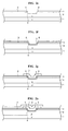
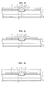
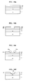
- Figs. 2a to 2k are cross-sectional views for illustrating a method of manufacturing a semiconductor device constructed in accordance with the first embodiment;
- Fig. 3 is a cross-sectional view of a semiconductor device constructed in accordance with a second embodiment of the invention;
- Fig. 4 is a cross-sectional view of a semiconductor device constructed in accordance with a third embodiment of the invention;
- Fig. 5 is a cross-sectional view of a semiconductor device constructed in accordance with a fourth embodiment of the invention;
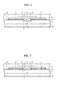
- Fig. 6 is a cross-sectional view of a semiconductor device constructed in accordance with a fifth embodiment of the invention;
- Fig. 7 is a cross-sectional view of a semiconductor device constructed in accordance with a sixth embodiment of the invention;
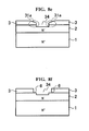
- Figs. 8a to 8f are cross-sectional views for illustrating a method of manufacturing a semiconductor device constructed in accordance with a seventh embodiment of the invention;
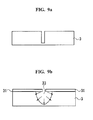
- Figs. 9a to 9b are cross-sectional views for illustrating the characteristics of an isotropic etching;
- Figs. 10a to 10d are cross-sectional views for illustrating a method of manufacturing a semiconductor device constructed in accordance with an eighth embodiment of the invention; and
- Figs. 11a to 11d are cross-sectional views for illustrating a method of manufacturing a semiconductor device constructed in accordance with a ninth embodiment of the invention.
- Referring firstly to Fig. 1, this is a cross-sectional view of a field effect transistor of a semiconductor device constructed in accordance with a first embodiment of the invention. In this transistor, two unit cells of the transistor are disposed in parallel and face each other. Although a plurality of unit cells may be connected in parallel to form a transistor, the above cross-sectional structure is explained below as a representative transistor.
- In Fig. 1, an N-type low concentrated (N-)
drain region 2 containing SiC is formed on a main surface of an N-type high concentrated (N+)substrate region 1 containing SiC. Thedrain region 2 is formed by an epitaxial layer grown on thesubstrate region 1. Thedrain region 2 forms a semiconductor substrate together with thesubstrate region 1. - Although there are several poly types (polycrystal) of SiC, this embodiment is explained with 4H-SiC as an example. It should be understood that the thicknesses of the
substrate region 1 and thedrain region 2 may not be drawn to scale in Fig. 1. In one embodiment, thesubstrate region 1 has a thickness of several hundreds of µm, whereas thedrain region 2 has a thickness ranging from several µm to several tens of µm. - An N+-type
hetero semiconductor region 3 containing a polycrystal silicon is formed on a main surface of thedrain region 2. The polycrystal silicon differs from SiC in terms of band gap and electron affinity. Therefore, a heterojunction is formed at both junction interfaces (for which the polycrystal silicon is used as a material for a hetero semiconductor region). - A
gate electrode 7 is formed adjacent to the junction portion of thedrain region 2 and thehetero semiconductor region 3 using thegate insulating film 5. Thehetero semiconductor region 3 is directly connected to a source electrode 9. Adrain electrode 10 is electrically and ohmically connected to an underside of thesubstrate region 1 at a low resistance. Thegate electrode 7 is insulated from the source electrode 9 by using aninterlayer insulating film 8. - A trench, which extends from a surface of the
hetero semiconductor region 3 to thedrain region 2, is formed. Further, thegate insulating film 5 and thegate electrode 7 are formed within the trench. Although the trench is formed in an inner portion of thedrain region 2 as shown in Fig. 1, the trench may be alternatively formed to extend to the junction interface of thehetero semiconductor region 3 and thedrain region 2. In this first embodiment, the driving point 6 (where thehetero semiconductor region 3, thedrain region 2 and thegate insulating film 5 are adjoined) is formed and located apart from the side wall of the trench. As used herein, a driving point refers to a location where the current flows from a source to a drain when a predetermined electric field is applied from a gate electrode. In one example herein, the source is a polysilicon region, and the drain is a SiC epilayer. - A method of manufacturing the device shown in Fig. 1 is now explained with reference to Figs 2a to 2k.
- First, as shown in Fig. 2a, the
drain region 2 containing an N--ype SiC is formed on the N+-type substrate region 1 by an epitaxial growth, etc. - Thereafter, a polycrystal silicon is deposited on the
drain region 2. A heterojunction is then formed between thedrain region 2 and thehetero semiconductor region 3. In such a configuration, a post-annealing may be performed in order to obtain a desired heterojunction characteristic by controlling the particle size or the grain boundary condition of the polycrystal silicon. Subsequently, impurities are introduced into the hetero semiconductor region 3 (which contains a hetero silicon) by, for example, using a mechanism such as ion injection. This is so that thehetero semiconductor region 3 can become an N+-type. Examples of the impurities include As (arsenic), P (phosphorous) and the like. This configuration is shown in Fig. 2b. - Next, a resist
pattern 21 corresponding to a mask material is formed on thehetero semiconductor region 3 as shown in Fig. 2c. Thehetero semiconductor region 3 and thedrain region 2 are selectively removed by dry etching using the resist pattern as a mask. The trench is formed such that abottom portion 4 of the trench reaches an inner portion of thedrain region 2. Alternatively, the mask material may be an oxide film. The etching may be performed with good controllability through a dry etching method, which uses ion or plasma to obtain a fine pattern. - Subsequently, after the mask material is removed, a
sacrificial oxide film 22 is formed by thermally oxidizing an exposed portion of the polycrystal silicon, i.e., thehetero semiconductor region 3. In such a case, a surface of thedrain region 2 containing SiC is also oxidized. However, since an oxidation ratio of SiC is smaller than that of the polycrystal silicon, the amount of the drain region 2 (containing SiC) being oxidized becomes smaller than that of thehetero semiconductor region 3 containing polycrystal silicon. This is shown in Fig. 2d. - Then, the
sacrificial oxide films 22 formed in the above process are removed using a fluoric acid based wet etching. As such, the trench-side end of the polycrystal silicon is receded from the side wall of the trench (shown in Fig. 2c) due to the difference between the oxidizing amounts of thedrain region 2 and thehetero semiconductor region 3. The driving point 6 (where thehetero semiconductor region 3, thedrain region 2 and the gate insulating film are adjoined) is formed by dry etching and located apart from the side wall of the trench. - Alternatively, after performing the dry etching process shown in Fig. 2c, the exposed portion may be removed through wet etching, which sets a certain selection ratio between polycristal silicon and SiC. By doing so, the configuration of Fig. 1 can be obtained (i.e., the
driving point 6 is spaced apart from the side wall of the trench). In another embodiment, it is possible to achieve this configuration by forming a resist material for the mask material used in the process shown in Fig. 2c. Then, the same wet etching can be performed after conducting a reduction process on the resist material through baking or UV irradiating. - As such, the trench may suffer from etching damage throughout a certain depth thereof depending on the condition of dry etching when forming the trench. However, the
driving point 6 at the edge portion of the junction end of thedrain region 2 and thehetero semiconductor region 3 is located apart from the side wall of the trench where the etching damage does not occur. Therefore, it is possible to form thedriving point 6 at a location not affected by the etching damage. - Further, a distance between the
driving point 6 and the side wall of the trench may be adjustable by controlling the oxidization amount in the process shown in Fig. 2d. Therefore, the distance can be set to be equal to or more than the range affected by the etching damage as shown in Fig. 2e. - Next, the
gate insulating film 5 is deposited on an entire surface of the device by using a deposition method such as CVD (Chemical Vapor Deposition) as shown in Fig. 2f. A suitable annealing treatment is performed on thegate insulating film 5. - Next, a polycrystal silicon corresponding to a
gate electrode 7 is deposited on thegate insulating film 5. Then impurities are introduced from a surface of thegate electrode 7 to pattern a desired configuration. This is shown in Fig. 2g. - As shown in Fig. 2h, an
interlayer insulating film 8 is next deposited on an entire surface of the device. - Subsequently, after removing the polycrystal silicon attached to the underside of the device, the
drain electrode 10 is formed of metal and is adjoined to thesubstrate region 1. Thereafter, a thermal treatment is performed thereon such that thedrain electrode 10 and thesubstrate region 1 are alloyed to ohmically connect to each other at a low resistance as shown in Fig. 2i. - In Fig. 2j, the
interlayer insulating film 8 is patterned to a desired configuration as shown. - Finally, as shown in Fig. 2k, a contact hole is formed, and the source electrode 9 is formed of metal to be adjoined with the
hetero semiconductor region 3 via the contact hole, thereby obtaining the device shown in Fig. 1. - The basic operation of a transistor, which is manufactured in accordance with the above, is the same as that of the conventional transistor. Hereinafter, the effects that can be achieved by the first embodiment are explained.
- First, as described above, the
driving point 6 of the transistor is formed at a location spaced apart from the side wall of the trench. Therefore, the driving point is not subject to the effect of etching damage occurring at the side wall of the trench by dry etching. Therefore, an interface level around thedriving point 6 is small and a grain thereof is maintained in an ideal state. When the device is in a conduction state, an electrical field from thegate electrode 7 is effectively applied to thedriving point 6. At the same time, the interface mobility around thedriving point 6 is increased. Accordingly, the driving power is improved, and the impedance can be sufficiently reduced. - Further, according to the first embodiment, the
gate electrode 7 is formed in the trench, which is formed in the inner portion of thedrain region 2. Accordingly, when the device is in a non-conduction state, the voltage of thegate electrode 7 positioned at a certain depth in thedrain region 2 is fixed to 0V. Further, it is possible to shield an electrical field formed by high voltage applied to thedrain electrode 10 at a deeper position. Therefore, the effect of lessening an electrical field around thedriving point 6 is increased such that a leak current can be reduced when the device is in an off state. - This could greatly contribute to miniaturization, scaling down and cost reduction of a power electronic system including a vehicle-mounting power electronic system.
- Fig. 3 illustrates the configuration of a semiconductor device constructed in accordance with a second embodiment of the invention. In the first embodiment shown in Fig. 1, the trench is formed in the inner portion of the
drain region 2 as shown in Fig. 2c. The second embodiment shown in Fig. 3 has a configuration similar to the first embodiment except that abottom portion 11 of the trench (a bottom portion of a dry etching surface) made by dry etching is positioned at a junction interface of thehetero semiconductor region 3 and thedrain region 2. - By adopting such a configuration, the oxide film is formed and removed after forming the trench in the same manner as in the first embodiment such that the
driving point 6 of the transistor is formed and located apart from the side wall of the trench, which is formed through etching. Thus, the driving point is not subject to the effect of etching damage occurring when forming the trench. Therefore, the second embodiment can achieve the same effect as the first embodiment. - Fig. 4 illustrates the configuration of a semiconductor device constructed in accordance with a third embodiment of the invention. The third embodiment shown in Fig. 4 has a configuration similar to the first embodiment except that a P-
type well region 12 is formed on an upper surface portion of thedrain region 2 to be adjoined with thehetero semiconductor region 3. The P-type well region 12 functions as an electrical field relaxing layer when the device is in a non-conduction state. - By adopting such a constitution including the electrical field relaxing layer, the effect of reducing a leak current when the element is non-conducted can be obtained in addition to the effects achieved by the first embodiment. Further, a device having a high pressure-resistance can be obtained with low impedance.
- Fig. 5 illustrates the configuration of a semiconductor device constructed in accordance with a fourth embodiment of the invention. The fourth embodiment shown in Fig. 5 has a configuration similar to the second embodiment except that a P-
type well region 12 is formed on an upper surface portion of thedrain region 2 to be adjoined with thehetero semiconductor region 3. The P-type well region 12 functions as an electrical field relaxing layer when the device is in a non-conduction state. - By adopting such a constitution including the electrical field relaxing layer, the effect of reducing a leak current when the device is in a non-conduction state can be obtained in addition to the effects achieved by the second embodiment. Further, a device having a high pressure-resistance can be obtained with low impedance.
- Fig. 6 illustrates the configuration of a semiconductor device constructed in accordance with a fifth embodiment of the invention. The fifth embodiment shown in Fig. 6 has a configuration similar to the first embodiment except that a P+-type
hetero semiconductor region 13 is formed under thehetero semiconductor region 3. - By adopting such a constitution, it is possible to form a barrier of the heterojunction interface to be higher by the P+-type
hetero semiconductor region 13. Further, in addition to the effects achieved by the first embodiment, a device having a higher pressure-resistance can be obtained. - Fig. 7 illustrates the configuration of a semiconductor device constructed in accordance with a sixth embodiment of the invention. The sixth embodiment shown in Fig. 7 has a configuration similar to the second embodiment except that a P+-type
hetero semiconductor region 13 is formed under thehetero semiconductor region 3. - By adopting such a constitution, it is possible to form a barrier of the heterojunction interface to be higher by the P+-type
hetero semiconductor region 13. Further, in addition to the effects achieved by the second embodiment, a device having a higher pressure-resistance can be obtained. - Also, in the first to sixth embodiments previously mentioned as well as the seventh to ninth embodiments explained below, the semiconductor substrate may contain gallium nitride or diamond in addition to silicon carbide. Further, in addition to polycrystal silicon, the hetero semiconductor region may include any one of single crystal silicon, amorphous silicon, single crystal silicon germanium, polycrystal silicon germanium and amorphous silicon germanium.
- Figs. 8a to 8f are cross-sectional views illustrating a method of manufacturing a semiconductor device constructed in accordance with a seventh embodiment of the invention. The seventh embodiment is another embodiment of the method for manufacturing the semiconductor device shown in Fig. 1. First, a
drain region 2 containing N--type SiC is formed on thesubstrate region 1 of N+-type SiC through an epitaxial growing process. Then, a polycrystal silicon is deposited on thedrain region 2 as ahetero semiconductor region 3, thereby forming a heterojunction between thedrain region 2 and thehetero semiconductor region 3. In such a case, a post-annealing may be performed in order to obtain a desired heterojunction characteristic by controlling the particle size or the grain boundary condition of the polycrystal silicon. Subsequently, impurities are introduced into thehetero semiconductor region 3 of a polycrystal silicon by using, for example, a mechanism such as ion injection so that thehetero semiconductor region 3 becomes N+-type. Examples of the impurities include As (arsenic), P (phosphorous) and the like. Then, a resist 31 corresponding to a mask material is applied on thehetero semiconductor region 3. This structure is shown in Fig. 8a. - Next, a
photomask 32 is formed on the resist 31 as shown in Fig. 8b. The resist 31 is selectively removed and patterned through etching using thephotomask 32. - After the
photomask 32 is removed, thehetero semiconductor region 3 of a polycrystal silicon is selectively removed through wet etching (i.e., isotropic etching) using the patterned resist 31 as a mask as shown in Fig. 8c. Alternatively, chemical dry etching may be used in this embodiment so long as it is an isotropic etching. - The characteristic of isotropic etching are explained below with reference to Figs. 9a to 9b. As shown in Fig. 9a, when a fine pattern such as a narrow
vertical trench 33 is to be formed on thehetero semiconductor region 3 by selectively etching the hetero semiconductor region via the patterned resist 31, a portion of thehetero semiconductor region 3 under the resist 31 may be etched. Accordingly, thehetero semiconductor region 3 may be laterally etched. As a result, as shown in Fig. 9b, the wall surface of thetrench 33 may be etched so as to have a curved surface. - Referring back to Fig. 8c, as explained with reference to Figs. 9a to 9b, in such an isotropic etching process, the etching of the
hetero semiconductor region 3 is advanced to a portion under the resist 31. Further, the thickness of the thinnest portion of thehetero semiconductor region 3 remaining after etching becomes about hundreds of angstroms (A). Further, although the etching surface of thehetero semiconductor region 3 is shown in a taper form in Fig. 8c for ease of explanation, the etching surface of thehetero semiconductor region 3 typically has a curved etching shape as shown in Fig. 9b. - Next, the
hetero semiconductor region 3 and thedrain region 2 are selectively removed through dry etching (i.e., anisotropic etching) by using the resist 31 as a mask. As such, atrench 34 is formed and a bottom portion thereof extends to thedrain region 2 as shown in Fig. 8d. - Thereafter, a
hetero semiconductor region 31 a, the thickness of which becomes gradually thinner, is obtained around thetrench 34 by removing the resist 31. For example, the thickness is about hundreds of A. Further, the length of thehetero semiconductor region 31a, the thickness of which becomes gradually thinner, is about thousands of A in the lateral direction from an end portion of thetrench 34. - Subsequently, a polycrystal silicon (i.e., hetero semiconductor region 3) and an exposed portion of the
drain region 2 are thermally oxidized to form a sacrificial oxide film. In such a case a bottom portion of thedrain region 2 of SiC is also oxidized. Since the oxidation ratio of SiC is smaller than that of a polycrystal silicon, however, the oxidation amount of thedrain region 2 of SiC becomes smaller than that of thehetero semiconductor region 3 of a polycrystal silicon. The sacrificial oxide films are then removed by fluoric acid based wet etching. Accordingly, thehetero semiconductor region 31 a, the thickness of which becomes thinner, is removed such that an end portion of thehetero semiconductor region 3 is receded from a side wall of thetrench 34. The driving point 6 (where thehetero semiconductor region 3, thedrain region 2 and thegate insulating film 5 are adjoined) is formed by dry etching and located apart from the side wall of thetrench 34 as shown in Fig. 8f. - Thereafter, such a semiconductor device shown in Fig. 1 is obtained through the processes illustrated in Figs. 2f to 2k, which are provided in relation to the first embodiment.
- Also in accordance with the seventh embodiment, a semiconductor device that has the characteristics of the first embodiment can be easily manufactured. Further, by employing the above manufacturing method, it is possible to lightly perform a sacrificial oxidation on the
hetero semiconductor region 3 in a longitudinal direction when forming thedriving point 6 in a position spaced apart from the etching surface by about thousands of A. Therefore, the amount of the sacrificial oxidization can be restrained, and a load of the manufacturing process can be reduced. Furthermore, the adverse effect caused by heavy sacrificial oxidization can be reduced. - Figs. 10a to 10d are cross-sectional views illustrating a method of manufacturing a semiconductor device constructed in accordance with an eighth embodiment of the invention. The eighth embodiment is another embodiment of the method for manufacturing such a semiconductor device as that shown in Fig. 1. First, a
drain region 2 of N-type SiC is formed on asubstrate region 1 of N+-type SiC through an epitaxial growing process. Then, a polycrystal silicon is deposited on thedrain region 2 as ahetero semiconductor region 3, thereby forming a heterojunction between thedrain region 2 and thehetero semiconductor region 3. In such a case, post-annealing may be performed in order to obtain a desired heterojunction characteristic by controlling the particle size or the grain boundary condition of the polycrystal silicon. Subsequently, impurities are introduced into thehetero semiconductor region 3 of a polycrystal silicon by using, for example, a mechanism such as ion injecting so that thehetero semiconductor region 3 becomes N+-type. Examples of the impurities include As (arsenic), P (phosphorous) and the like. Then, a resist 31 corresponding to a mask material is applied on thehetero semiconductor region 3. This structure is shown in Fig. 10a. - A
photomask 32 is next formed on the resist 31. The resist 31 is selectively removed and patterned through etching by using thephotomask 32 as shown in Fig. 10b. - The resist 31 is then removed by isotropic wet etching. Accordingly, the edge portion of an upper end of the resist 31 is isotropically etched and removed, thereby obtaining an
edge portion 31 a in a taper form as shown in Fig. 10c. - Next, dry etching (i.e., anisotropic etching) is performed to selectively remove the
hetero semiconductor region 3 and thedrain region 2 by using the resist 31, theedge portion 31a of which has a taper form, as a mask. As such, atrench 35 is formed such that a bottom portion thereof extends to thedrain region 2. In such a case, eachedge portion 31a of the resist 31 having a taper form is more rapidly etched than the other portions of the resist 31 through anisotropic etching. Thus, the underlyinghetero semiconductor region 3 is etched. As a result, a portion of thehetero semiconductor region 3, the thickness of which becomes gradually thinner, is formed around thetrench 35 as shown in Fig. 10d. That is, the shape of the resist 31 is transferred into thehetero semiconductor region 3. The thickness of the thinner portion of thehetero semiconductor region 3 is about thousands of A. Further, a length of thehetero semiconductor region 3, the thickness of which becomes thinner, is about thousands of A in the lateral direction from an end of thetrench 35. - Thereafter, the semiconductor device shown in Fig. 1 is obtained through the processes shown in Figs. 2f to 2k and Figs. 8e and 8f, which have been explained above in relation to the first and seventh embodiments.
- Also in accordance with the eighth embodiment, a semiconductor device, which has the characteristics of the first embodiment, can be easily manufactured. Further, the resist 31 on an uppermost surface is processed by employing the above-described method. As such, the manufacturing process proceeds while monitoring the shape of a device produced during the manufacturing process.
- Figs. 11a to 11d are cross-sectional views illustrating a method of manufacturing a semiconductor device constructed in accordance with a ninth embodiment of the invention. The ninth embodiment is another embodiment of a method for manufacturing a semiconductor device as shown in Fig. 1. First, the
drain region 2 of N--type SiC is formed on thesubstrate region 1 of N+-type SiC through an epitaxial growing process. Then, a polycrystal silicon is deposited on thedrain region 2 as ahetero semiconductor region 3, thereby forming a heterojunction between the polycrystal silicon and thedrain region 2. In such a case post-annealing may be performed in order to obtain a desired heterojunction characteristic by controlling the particle size or the grain boundary condition of the polycrystal silicon. Subsequently, impurities are introduced into thehetero semiconductor region 3 of a polycrystal silicon by using, for example, a mechanism such as ion injection. This is done so that thehetero semiconductor region 3 becomes N+-type. Examples of the impurities include As (arsenic), P (phosphorous) and the like. Then, a resist 31 corresponding to a mask material is applied on thehetero semiconductor region 3. The resulting structure is shown in Fig. 11a. - A
photomask 32 is next formed on the resist 31. The resist 31 is selectively removed and patterned through etching by using thephotomask 32 as shown in Fig. 11b. - Then, after the
photomask 32 is removed, thehetero semiconductor region 3 of a polycrystal silicon is selectively removed through wet etching (i.e., isotropic etching) by using the patterned resist 31 as a mask as shown in Fig. 11c. Alternatively, chemical dry etching may be used in this embodiment so long as it is an isotropic etching. In the isotropic etching process, a portion of thehetero semiconductor region 3 under the resist 31 may be etched in a similar manner as explained with reference to Figs. 9a to 9b. Further, the thickness of the thinnest portion of the etchedhetero semiconductor region 2 becomes hundreds of A. Although the etching surface of thehetero semiconductor region 3 is shown to have a tapered shape in Fig. 11c for ease of explanation, the etching surface of thehetero semiconductor 3 typically has a curved shape as shown in Fig. 9b. - After the resist 31 is removed, a resist 36 is additionally applied on the
hetero semiconductor region 3. The resist 36 is then selectively removed and patterned. Thereafter, thehetero semiconductor region 3 and thedrain region 2 are selectively removed through dry etching (i.e., anisotropic etching) by using the patterned resist 36 as a mask. Accordingly, atrench 37 is formed such that a bottom portion thereof extends to thedrain region 2 as shown in Fig. 11d. - Thereafter, the semiconductor device shown in Fig. 1 is obtained through the processes shown in Figs. 2f to 2k and Figs. 8e and 8f, which have already been explained in relation to the first and seventh embodiments.
- According to the ninth embodiment, a semiconductor device, which has the characteristics of the first embodiment, can be easily manufactured. Further, by employing the above method, it is possible to form a device without being affected by the recession of a resist in the etching process.
- Further, in the seventh to ninth embodiments, an oxide film may be used as a mask material instead of a resist.
- Also, the above-described embodiments have been described in order to allow easy understanding of the present invention and do not limit the present invention. On the contrary, the invention is intended to cover various modifications and equivalent arrangements included within the scope of the appended claims, which scope is to be accorded the broadest interpretation so as to encompass all such modifications and equivalent structure as is permitted under the law.
- This application claims priority from
Japanese Patent Application No. 2006-079107, filed 22nd March 2006
Claims (13)
- A semiconductor device, comprising:a semiconductor substrate of a first conductive-type, the semiconductor substrate having a trench formed therein;a heterojunction forming portion adjoined to a main surface of the semiconductor substrate and forming a heterojunction with the semiconductor substrate;a gate electrode disposed adjacent to a junction end of the heterojunction forming portion and the semiconductor substrate using a gate insulating film;a source electrode connected to the heterojunction forming portion;a drain electrode connected to the semiconductor substrate; anda driving point of the semiconductor substrate where the gate insulating film, the hetero semiconductor region and the semiconductor substrate are adjoined is at a position spaced apart from a side wall of the trench.
- A semiconductor device as claimed in claim 1 wherein the heterojunction forming portion around the driving point is of the first conductive-type.
- A semiconductor device as claimed in claim 1 or claim 2 wherein the semiconductor substrate comprises at least one of a silicon carbide, a gallium nitride and a diamond.
- A semiconductor device as claimed in any preceding claim wherein the heterojunction forming portion comprises at least one of a single crystal silicon, a polycrystal silicon, an amorphous silicon, a single silicon germanium, a polycrystal silicon germanium and an amorphous silicon germanium.
- A method of manufacturing a semiconductor device, comprising:depositing a hetero semiconductor region on a semiconductor substrate of a first conductive-type, wherein the hetero semiconductor region forms a heterojunction with the semiconductor substrate;forming a trench by selectively removing portions of the semiconductor substrate and the hetero semiconductor region by a dry etching; forming a sacrificial oxide film by thermally oxidizing the semiconductor substrate and the hetero semiconductor region forming at least a side wall of the trench;removing the sacrificial oxide film;forming a gate insulating film on an exposed surface of the semiconductor substrate and the hetero semiconductor region including an inner surface of the trench after removing the sacrificial oxide film;forming a gate electrode adjacent to a junction end of the semiconductor substrate and the hetero semiconductor region using the gate insulating film;forming a source electrode connected to the hetero semiconductor region; andforming a drain electrode connected to the semiconductor substrate; and wherein a device driving point where the gate insulating film, the hetero semiconductor region and the semiconductor substrate are adjoined is at a position spaced apart from a side wall of the trench.
- A method as claimed in claim 5 wherein forming the source electrode connected to the hetero semiconductor region occurs after forming the gate electrode and/or forming the drain electrode connected to the semiconductor substrate occurs after forming the source electrode.
- A method of manufacturing a semiconductor device, comprising:depositing a hetero semiconductor region on a semiconductor substrate of a first conductive-type, wherein the hetero semiconductor region forms a heterojunction with the semiconductor substrate;forming a trench by selectively removing the semiconductor substrate and the hetero semiconductor region by a dry etching;selectively etching the semiconductor substrate and the hetero semiconductor region by a wet etching, wherein the wet etching has different selecting ratios for the semiconductor substrate and the hetero semiconductor region;forming a gate insulating film in the semiconductor substrate and the hetero semiconductor region including an inner surface of the trench after selectively etching the semiconductor substrate and the hetero semiconductor region by the wet etching;forming a gate electrode adjacent to a junction end of the semiconductor substrate and the hetero semiconductor region using the gate insulating film;forming a source electrode connected to the hetero semiconductor region; andforming a drain electrode connected to the semiconductor substrate; and wherein a driving point of the semiconductor device where the gate insulating film, the hetero semiconductor region and the semiconductor substrate are adjoined is at a position spaced apart from a side wall of the trench.
- A method as claimed in claim 7 wherein forming the trench by selectively removing the semiconductor substrate and the hetero semiconductor region by the dry etching includes selectively removing the semiconductor substrate and the hetero semiconductor region using a mask material and wherein the method comprises reducing the mask material used in selectively removing the semiconductor substrate and the hetero semiconductor region prior to selectively etching the semiconductor substrate and the hetero semiconductor region by the wet etching.
- A method of manufacturing a semiconductor device, comprising:depositing a hetero semiconductor region on a first conductive-type semiconductor substrate, wherein the hetero semiconductor region forms a heterojunction with the semiconductor substrate;forming a trench by selectively removing the hetero semiconductor region by a dry etching, wherein a bottom surface of the trench is a junction interface of the semiconductor substrate and the hetero semiconductor region;forming a sacrificial oxide film by thermally oxidizing the semiconductor substrate and the hetero semiconductor region forming at least an inner portion of the trench;removing the sacrificial oxide film;forming a gate insulating film on the semiconductor substrate and the hetero semiconductor region including the inner surface of the trench after removing the sacrificial oxide film;forming a gate electrode adjacent to a junction end of the semiconductor substrate and the hetero semiconductor region using the gate insulating film;forming a source electrode connected to the hetero semiconductor region; andforming a drain electrode connected to the semiconductor substrate; and wherein a driving point of the semiconductor device where the gate insulating film, the hetero semiconductor region and the semiconductor substrate are adjoined is formed at a position spaced apart from a side wall of the trench before forming the sacrificial oxide film.
- A method of manufacturing a semiconductor device, comprising:depositing a hetero semiconductor region on a first conductive-type semiconductor substrate, wherein the hetero semiconductor region forms a heterojunction with the semiconductor substrate;forming a trench wherein a bottom portion of the trench extends to the semiconductor substrate and a thickness of a portion of the hetero semiconductor region around the trench is smaller than a thickness of other portions of the hetero semiconductor region, wherein forming the trench includes selectively removing the semiconductor substrate and the hetero semiconductor region by an isotropic etching;forming a sacrificial oxide film by thermally oxidizing at least the hetero semiconductor region after forming the trench;selectively removing the portion of the hetero semiconductor region around the trench smaller that the thickness of the other portions by removing the sacrificial oxide film;forming the gate insulating film on the semiconductor substrate and the hetero semiconductor region including an inner surface of the trench after removing the sacrificial oxide film;forming a gate electrode adjacent to a junction end of the semiconductor substrate and the hetero semiconductor region using the gate insulating film;forming a source electrode connected to the hetero semiconductor region; andforming a drain electrode connected to the semiconductor substrate; and wherein a driving point of the semiconductor device where the gate insulating film, the hetero semiconductor region and the semiconductor substrate are adjoined is at a position spaced apart from a side wall of the trench.
- A method as claimed in claim 10 wherein forming the trench comprises:performing an anisotropic etching by using a mask pattern used in the isotropic etching after performing the isotropic etching; andselectively removing the semiconductor substrate and the hetero semiconductor region after performing the anisotropic etching and before forming the sacrificial oxide film.
- A method as claimed in claim 10 or claim 11 wherein forming the trench comprises:selectively removing, through an anisotropic etching, an edge portion of a mask pattern used by the isotropic etching; andselectively removing the semiconductor substrate and the hetero semiconductor region using the mask pattern after the anisotropic etching and before forming the sacrificial oxide film.
- A method as claimed in any of claims 10 to 12 wherein the semiconductor substrate comprises at least one of a silicon carbide, a gallium nitride and a diamond, and wherein the hetero semiconductor region comprises at least one of a single crystal silicon, a polycrystal silicon, an amorphous silicon, a single silicon germanium, a polycrystal silicon germanium and an amorphous silicon germanium.
Applications Claiming Priority (1)
| Application Number | Priority Date | Filing Date | Title |
|---|---|---|---|
| JP2006079107 | 2006-03-22 |
Publications (3)
| Publication Number | Publication Date |
|---|---|
| EP1837915A2 true EP1837915A2 (en) | 2007-09-26 |
| EP1837915A3 EP1837915A3 (en) | 2008-10-01 |
| EP1837915B1 EP1837915B1 (en) | 2017-07-05 |
Family
ID=38171249
Family Applications (1)
| Application Number | Title | Priority Date | Filing Date |
|---|---|---|---|
| EP07104449.9A Ceased EP1837915B1 (en) | 2006-03-22 | 2007-03-20 | Semiconductors |
Country Status (4)
| Country | Link |
|---|---|
| US (1) | US8441036B2 (en) |
| EP (1) | EP1837915B1 (en) |
| KR (1) | KR100944858B1 (en) |
| CN (1) | CN100508213C (en) |
Families Citing this family (8)
| Publication number | Priority date | Publication date | Assignee | Title |
|---|---|---|---|---|
| JP5228291B2 (en) * | 2006-07-06 | 2013-07-03 | 日産自動車株式会社 | Manufacturing method of semiconductor device |
| JP5211468B2 (en) * | 2006-11-24 | 2013-06-12 | 日産自動車株式会社 | Manufacturing method of semiconductor device |
| US8067776B2 (en) * | 2007-06-08 | 2011-11-29 | Nissan Motor Co., Ltd. | Method of manufacturing semiconductor device and semiconductor device manufactured thereof |
| CN102386223B (en) * | 2011-11-01 | 2013-08-14 | 中山大学 | High-threshold voltage gallium nitride (GaN) enhancement metal oxide semiconductor heterostructure field effect transistor (MOSHFET) device and manufacturing method |
| JP2013110331A (en) * | 2011-11-24 | 2013-06-06 | Sumitomo Electric Ind Ltd | Semiconductor device manufacturing method |
| CN108711549A (en) * | 2018-04-28 | 2018-10-26 | 西安交通大学 | Ultrathin alumina dielectric layer diamond field effect transistor and preparation method thereof |
| CN117241483B (en) * | 2023-10-25 | 2024-04-12 | 广东达源设备科技有限公司 | Spraying device and method for circuit board production |
| CN118588736A (en) * | 2024-05-20 | 2024-09-03 | 重庆奕能科技有限公司 | Semiconductor Devices |
Family Cites Families (9)
| Publication number | Priority date | Publication date | Assignee | Title |
|---|---|---|---|---|
| US4992390A (en) | 1989-07-06 | 1991-02-12 | General Electric Company | Trench gate structure with thick bottom oxide |
| JPH10275865A (en) | 1997-03-31 | 1998-10-13 | Nec Kyushu Ltd | Semiconductor device and manufacturing method thereof |
| US6194741B1 (en) | 1998-11-03 | 2001-02-27 | International Rectifier Corp. | MOSgated trench type power semiconductor with silicon carbide substrate and increased gate breakdown voltage and reduced on-resistance |
| JP2002314096A (en) | 2001-04-16 | 2002-10-25 | Auto Network Gijutsu Kenkyusho:Kk | Junction type field effect transistor and method of manufacturing the same |
| KR20030042325A (en) * | 2001-11-22 | 2003-05-28 | 주식회사 엘지이아이 | Fabrication Method for Heterojunction Field Effect Transistor |
| JP4004843B2 (en) | 2002-04-24 | 2007-11-07 | Necエレクトロニクス株式会社 | Method for manufacturing vertical MOSFET |
| US6927414B2 (en) * | 2003-06-17 | 2005-08-09 | International Business Machines Corporation | High speed lateral heterojunction MISFETs realized by 2-dimensional bandgap engineering and methods thereof |
| EP2560210B1 (en) | 2003-09-24 | 2018-11-28 | Nissan Motor Co., Ltd. | Semiconductor device and manufacturing method thereof |
| JP4439955B2 (en) | 2004-03-15 | 2010-03-24 | パナソニック株式会社 | Semiconductor device and manufacturing method of semiconductor laser device |
-
2007
- 2007-03-15 US US11/724,389 patent/US8441036B2/en not_active Expired - Fee Related
- 2007-03-20 EP EP07104449.9A patent/EP1837915B1/en not_active Ceased
- 2007-03-21 KR KR1020070027382A patent/KR100944858B1/en not_active Expired - Fee Related
- 2007-03-22 CN CNB2007100869286A patent/CN100508213C/en not_active Expired - Fee Related
Also Published As
| Publication number | Publication date |
|---|---|
| KR100944858B1 (en) | 2010-03-04 |
| CN100508213C (en) | 2009-07-01 |
| US8441036B2 (en) | 2013-05-14 |
| EP1837915B1 (en) | 2017-07-05 |
| CN101043054A (en) | 2007-09-26 |
| KR20070095795A (en) | 2007-10-01 |
| US20070221955A1 (en) | 2007-09-27 |
| EP1837915A3 (en) | 2008-10-01 |
Similar Documents
| Publication | Publication Date | Title |
|---|---|---|
| US12295156B2 (en) | Semiconductor device including trench gate structure and buried shielding region and method of manufacturing | |
| JP5862729B2 (en) | Manufacturing method of trench gate type semiconductor device | |
| US9525057B2 (en) | Semiconductor device | |
| CN101188201B (en) | Method for manufacturing semiconductor device | |
| US8564060B2 (en) | Semiconductor device with large blocking voltage and manufacturing method thereof | |
| CN102270660B (en) | Method for forming trench type metal oxide semiconductor field effect transistor | |
| JP5102411B2 (en) | Semiconductor device and manufacturing method thereof | |
| EP1837915B1 (en) | Semiconductors | |
| US11631764B2 (en) | Manufacturing method of semiconductor device and semiconductor device | |
| JPWO2008123491A1 (en) | Semiconductor device using carrier multiplication by ionizing collision and method for manufacturing the same | |
| US7923330B2 (en) | Method for manufacturing a semiconductor device | |
| JP2011238726A (en) | Semiconductor device and method of manufacturing the same | |
| CA3025767C (en) | Semiconductor device | |
| CN116368624B (en) | Semiconductor device and method for manufacturing the same | |
| KR101091195B1 (en) | Silicon carbide LMOSFET | |
| JP5167592B2 (en) | Semiconductor device and manufacturing method thereof | |
| JP2007288118A (en) | Semiconductor device and manufacturing method thereof |
Legal Events
| Date | Code | Title | Description |
|---|---|---|---|
| PUAI | Public reference made under article 153(3) epc to a published international application that has entered the european phase |
Free format text: ORIGINAL CODE: 0009012 |
|
| AK | Designated contracting states |
Kind code of ref document: A2 Designated state(s): AT BE BG CH CY CZ DE DK EE ES FI FR GB GR HU IE IS IT LI LT LU LV MC MT NL PL PT RO SE SI SK TR |
|
| AX | Request for extension of the european patent |
Extension state: AL BA HR MK YU |
|
| PUAL | Search report despatched |
Free format text: ORIGINAL CODE: 0009013 |
|
| AK | Designated contracting states |
Kind code of ref document: A3 Designated state(s): AT BE BG CH CY CZ DE DK EE ES FI FR GB GR HU IE IS IT LI LT LU LV MC MT NL PL PT RO SE SI SK TR |
|
| AX | Request for extension of the european patent |
Extension state: AL BA HR MK RS |
|
| 17P | Request for examination filed |
Effective date: 20090401 |
|
| 17Q | First examination report despatched |
Effective date: 20090511 |
|
| AKX | Designation fees paid |
Designated state(s): DE FR GB |
|
| GRAP | Despatch of communication of intention to grant a patent |
Free format text: ORIGINAL CODE: EPIDOSNIGR1 |
|
| INTG | Intention to grant announced |
Effective date: 20170331 |
|
| RIC1 | Information provided on ipc code assigned before grant |
Ipc: H01L 29/423 20060101ALI20170321BHEP Ipc: H01L 29/267 20060101ALI20170321BHEP Ipc: H01L 21/3213 20060101ALI20170321BHEP Ipc: H01L 21/027 20060101ALI20170321BHEP Ipc: H01L 21/336 20060101ALI20170321BHEP Ipc: H01L 29/16 20060101ALN20170321BHEP Ipc: H01L 29/78 20060101AFI20170321BHEP |
|
| RIN1 | Information on inventor provided before grant (corrected) |
Inventor name: SHIMOIDA, YOSHIO Inventor name: TANAKA, HIDEAKI Inventor name: HAYASHI, TETSUYA Inventor name: HOSHI, MASAKATSU Inventor name: YAMAGAMI, SHIGEHARU |
|
| GRAS | Grant fee paid |
Free format text: ORIGINAL CODE: EPIDOSNIGR3 |
|
| GRAA | (expected) grant |
Free format text: ORIGINAL CODE: 0009210 |
|
| AK | Designated contracting states |
Kind code of ref document: B1 Designated state(s): DE FR GB |
|
| REG | Reference to a national code |
Ref country code: GB Ref legal event code: FG4D |
|
| REG | Reference to a national code |
Ref country code: DE Ref legal event code: R096 Ref document number: 602007051528 Country of ref document: DE |
|
| REG | Reference to a national code |
Ref country code: FR Ref legal event code: PLFP Year of fee payment: 12 |
|
| REG | Reference to a national code |
Ref country code: DE Ref legal event code: R097 Ref document number: 602007051528 Country of ref document: DE |
|
| PLBE | No opposition filed within time limit |
Free format text: ORIGINAL CODE: 0009261 |
|
| STAA | Information on the status of an ep patent application or granted ep patent |
Free format text: STATUS: NO OPPOSITION FILED WITHIN TIME LIMIT |
|
| 26N | No opposition filed |
Effective date: 20180406 |
|
| PGFP | Annual fee paid to national office [announced via postgrant information from national office to epo] |
Ref country code: FR Payment date: 20230222 Year of fee payment: 17 |
|
| PGFP | Annual fee paid to national office [announced via postgrant information from national office to epo] |
Ref country code: GB Payment date: 20230222 Year of fee payment: 17 Ref country code: DE Payment date: 20230221 Year of fee payment: 17 |
|
| REG | Reference to a national code |
Ref country code: DE Ref legal event code: R119 Ref document number: 602007051528 Country of ref document: DE |
|
| GBPC | Gb: european patent ceased through non-payment of renewal fee |
Effective date: 20240320 |
|
| PG25 | Lapsed in a contracting state [announced via postgrant information from national office to epo] |
Ref country code: DE Free format text: LAPSE BECAUSE OF NON-PAYMENT OF DUE FEES Effective date: 20241001 |
|
| PG25 | Lapsed in a contracting state [announced via postgrant information from national office to epo] |
Ref country code: GB Free format text: LAPSE BECAUSE OF NON-PAYMENT OF DUE FEES Effective date: 20240320 |
|
| PG25 | Lapsed in a contracting state [announced via postgrant information from national office to epo] |
Ref country code: FR Free format text: LAPSE BECAUSE OF NON-PAYMENT OF DUE FEES Effective date: 20240331 |
|
| PG25 | Lapsed in a contracting state [announced via postgrant information from national office to epo] |
Ref country code: GB Free format text: LAPSE BECAUSE OF NON-PAYMENT OF DUE FEES Effective date: 20240320 Ref country code: FR Free format text: LAPSE BECAUSE OF NON-PAYMENT OF DUE FEES Effective date: 20240331 Ref country code: DE Free format text: LAPSE BECAUSE OF NON-PAYMENT OF DUE FEES Effective date: 20241001 |