EP1835624A2 - Power management in a data acquisition system - Google Patents
Power management in a data acquisition system Download PDFInfo
- Publication number
- EP1835624A2 EP1835624A2 EP07004908A EP07004908A EP1835624A2 EP 1835624 A2 EP1835624 A2 EP 1835624A2 EP 07004908 A EP07004908 A EP 07004908A EP 07004908 A EP07004908 A EP 07004908A EP 1835624 A2 EP1835624 A2 EP 1835624A2
- Authority
- EP
- European Patent Office
- Prior art keywords
- amplifier
- gain
- current level
- data acquisition
- control signals
- Prior art date
- Legal status (The legal status is an assumption and is not a legal conclusion. Google has not performed a legal analysis and makes no representation as to the accuracy of the status listed.)
- Withdrawn
Links
Images


Classifications
-
- H—ELECTRICITY
- H03—ELECTRONIC CIRCUITRY
- H03F—AMPLIFIERS
- H03F3/00—Amplifiers with only discharge tubes or only semiconductor devices as amplifying elements
- H03F3/45—Differential amplifiers
- H03F3/45071—Differential amplifiers with semiconductor devices only
- H03F3/45076—Differential amplifiers with semiconductor devices only characterised by the way of implementation of the active amplifying circuit in the differential amplifier
- H03F3/45179—Differential amplifiers with semiconductor devices only characterised by the way of implementation of the active amplifying circuit in the differential amplifier using MOSFET transistors as the active amplifying circuit
- H03F3/45183—Long tailed pairs
- H03F3/45188—Non-folded cascode stages
-
- H—ELECTRICITY
- H03—ELECTRONIC CIRCUITRY
- H03F—AMPLIFIERS
- H03F3/00—Amplifiers with only discharge tubes or only semiconductor devices as amplifying elements
- H03F3/45—Differential amplifiers
- H03F3/45071—Differential amplifiers with semiconductor devices only
- H03F3/45076—Differential amplifiers with semiconductor devices only characterised by the way of implementation of the active amplifying circuit in the differential amplifier
- H03F3/45475—Differential amplifiers with semiconductor devices only characterised by the way of implementation of the active amplifying circuit in the differential amplifier using IC blocks as the active amplifying circuit
-
- H—ELECTRICITY
- H03—ELECTRONIC CIRCUITRY
- H03G—CONTROL OF AMPLIFICATION
- H03G1/00—Details of arrangements for controlling amplification
- H03G1/0005—Circuits characterised by the type of controlling devices operated by a controlling current or voltage signal
- H03G1/0017—Circuits characterised by the type of controlling devices operated by a controlling current or voltage signal the device being at least one of the amplifying solid-state elements
- H03G1/0029—Circuits characterised by the type of controlling devices operated by a controlling current or voltage signal the device being at least one of the amplifying solid-state elements using field-effect transistors [FET]
-
- H—ELECTRICITY
- H03—ELECTRONIC CIRCUITRY
- H03G—CONTROL OF AMPLIFICATION
- H03G1/00—Details of arrangements for controlling amplification
- H03G1/0005—Circuits characterised by the type of controlling devices operated by a controlling current or voltage signal
- H03G1/0088—Circuits characterised by the type of controlling devices operated by a controlling current or voltage signal using discontinuously variable devices, e.g. switch-operated
-
- H—ELECTRICITY
- H03—ELECTRONIC CIRCUITRY
- H03M—CODING; DECODING; CODE CONVERSION IN GENERAL
- H03M1/00—Analogue/digital conversion; Digital/analogue conversion
- H03M1/12—Analogue/digital converters
- H03M1/124—Sampling or signal conditioning arrangements specially adapted for A/D converters
- H03M1/129—Means for adapting the input signal to the range the converter can handle, e.g. limiting, pre-scaling ; Out-of-range indication
-
- H—ELECTRICITY
- H03—ELECTRONIC CIRCUITRY
- H03F—AMPLIFIERS
- H03F2200/00—Indexing scheme relating to amplifiers
- H03F2200/331—Sigma delta modulation being used in an amplifying circuit
-
- H—ELECTRICITY
- H03—ELECTRONIC CIRCUITRY
- H03F—AMPLIFIERS
- H03F2203/00—Indexing scheme relating to amplifiers with only discharge tubes or only semiconductor devices as amplifying elements covered by H03F3/00
- H03F2203/45—Indexing scheme relating to differential amplifiers
- H03F2203/45032—Indexing scheme relating to differential amplifiers the differential amplifier amplifying transistors are multiple paralleled transistors
-
- H—ELECTRICITY
- H03—ELECTRONIC CIRCUITRY
- H03F—AMPLIFIERS
- H03F2203/00—Indexing scheme relating to amplifiers with only discharge tubes or only semiconductor devices as amplifying elements covered by H03F3/00
- H03F2203/45—Indexing scheme relating to differential amplifiers
- H03F2203/45371—Indexing scheme relating to differential amplifiers the AAC comprising parallel coupled multiple transistors at their source and gate and drain or at their base and emitter and collector, e.g. in a cascode dif amp, only those forming the composite common source transistor or the composite common emitter transistor respectively
-
- H—ELECTRICITY
- H03—ELECTRONIC CIRCUITRY
- H03F—AMPLIFIERS
- H03F2203/00—Indexing scheme relating to amplifiers with only discharge tubes or only semiconductor devices as amplifying elements covered by H03F3/00
- H03F2203/45—Indexing scheme relating to differential amplifiers
- H03F2203/45396—Indexing scheme relating to differential amplifiers the AAC comprising one or more switches
-
- H—ELECTRICITY
- H03—ELECTRONIC CIRCUITRY
- H03F—AMPLIFIERS
- H03F2203/00—Indexing scheme relating to amplifiers with only discharge tubes or only semiconductor devices as amplifying elements covered by H03F3/00
- H03F2203/45—Indexing scheme relating to differential amplifiers
- H03F2203/45486—Indexing scheme relating to differential amplifiers the CSC comprising two or more paralleled transistors as current source
-
- H—ELECTRICITY
- H03—ELECTRONIC CIRCUITRY
- H03F—AMPLIFIERS
- H03F2203/00—Indexing scheme relating to amplifiers with only discharge tubes or only semiconductor devices as amplifying elements covered by H03F3/00
- H03F2203/45—Indexing scheme relating to differential amplifiers
- H03F2203/45504—Indexing scheme relating to differential amplifiers the CSC comprising more than one switch
-
- H—ELECTRICITY
- H03—ELECTRONIC CIRCUITRY
- H03F—AMPLIFIERS
- H03F2203/00—Indexing scheme relating to amplifiers with only discharge tubes or only semiconductor devices as amplifying elements covered by H03F3/00
- H03F2203/45—Indexing scheme relating to differential amplifiers
- H03F2203/45631—Indexing scheme relating to differential amplifiers the LC comprising one or more capacitors, e.g. coupling capacitors
-
- H—ELECTRICITY
- H03—ELECTRONIC CIRCUITRY
- H03F—AMPLIFIERS
- H03F2203/00—Indexing scheme relating to amplifiers with only discharge tubes or only semiconductor devices as amplifying elements covered by H03F3/00
- H03F2203/45—Indexing scheme relating to differential amplifiers
- H03F2203/45634—Indexing scheme relating to differential amplifiers the LC comprising one or more switched capacitors
-
- H—ELECTRICITY
- H03—ELECTRONIC CIRCUITRY
- H03F—AMPLIFIERS
- H03F2203/00—Indexing scheme relating to amplifiers with only discharge tubes or only semiconductor devices as amplifying elements covered by H03F3/00
- H03F2203/45—Indexing scheme relating to differential amplifiers
- H03F2203/45726—Indexing scheme relating to differential amplifiers the LC comprising more than one switch, which are not cross coupled
Definitions
- the invention relates generally to electronic processing arrangements in a data acquisition system. More particularly, it relates to a method for reducing overall power in a data acquisition system.
- the present invention has use especially, but not exclusively, in the field of seismic sensing applications where it is desired to achieve significant power savings.
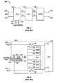
- a typical data acquisition system 100 comprises a PGA (programmable gain amplifier) block 102, an ADC (analog-to-digital converter) block 104, and a decimation filter block 106, as shown in Figure 1 and labeled as "Prior Art.”
- the system 100 may be used for converting an analog input signal of a signal source (seismic sensor or transducer) to a digital output signal.
- the analog input signal is applied through input terminals 108, 110 to the PGA block 102 which, in turn, produces an amplified signal on its output lines 112, 114.
- the output lines 112, 114 from the PGA block 102 are coupled to the input of the ADC block 104 which generates a digitized signal on its output lines 116, 118.
- the digitized signal is passed to the decimation filter block 106 which produces the filtered digital output signal on output terminals 120, 122.
- the gain of the PGA block 102 is controlled by gain control signals at gain control lines 124 - 128. Since the input terminals 108, 110 may receive different input signals each having different voltage characteristics, the amount of amplification required to be provided by the amplifier block 102 can be adjusted via the signals applied at gain control lines 124 - 128 depending upon the signal level applied to the input terminals 108, 110.
- the total noise power of a channel in the digital acquisition system 100 is given by the sum (in RMS sense) of the noise power of the amplifier block 102 and the noise power of the ADC block 104.
- the use of the PGA block 102 will reduce the ADC block's noise when that noise is input-referred to the PGA block's input.
- the "input-referred" noise at the input of the PGA block 102 means the noise of the ADC block 104 divided by the gain of the PGA block.
- the PGA block 102 is typically designed and rated for its input-referred noise. As the gain of the amplifier block 102 is increased, the noise at its output on lines 112, 114 will also be increased. Accordingly, at a lower gain setting of the PGA block 102, the contribution of the noise power from the amplifier will be invariably small when compared to the noise power from the ADC block 104, as the ADC block 104 may have a relatively high noise power.
- the use of the PGA block 102 in the data acquisition system 100 of Figure 1 suffers from a drawback of being power inefficient since there is no control of the power in either the amplifier block 102 and/or the ADC block 104 when the gain settings in the PGA block 102 are changed. It would therefore be desirable to provide a technique that reduces the overall power in a data acquisition system when the gain settings of the PGA block 102 are modified.
- a data acquisition system which includes a programmable gain amplifier, an analog-to-digital converter, a filter, and control circuitry.
- the programmable gain amplifier is operatively connected to receive an analog input signal on its input and generates an amplified signal on its output in accordance with gain control signals.
- the analog-to-digital converter is operatively connected to receive the amplified signal from the amplifier and generates a digitized signal on its output.
- the filter is operatively connected to receive the digitized signal from the converter and generates a filtered digital signal on its output.
- the control circuitry is operatively connected to the amplifier and to the converter and is also responsive to the gain control signals for dynamically adjusting power between the amplifier and the converter when the gain control signals are changed.
- FIG 1 is a block diagram of a conventional data acquisition system, which has been labeled "Prior Art";
- FIG. 2 is a more detailed block diagram of the PGA block 102 of Figure 1, illustrating an exemplary gain control circuitry and labeled "Prior Art";
- FIG. 3 is a block diagram of a data acquisition system, constructed in accordance with principles of the present invention.
- Figure 4 is a representation of one circuit design of one of the amplifiers 130, 132 for implementing the PGA block 202 of Figure 3;
- Figure 5 is a schematic circuit diagram for implementing a portion of one stage of the multi-stage amplifier 400 of Figure 4.
- Figure 6 is a schematic circuit diagram for implementing the front end portion of a switched capacitor delta-sigma modulator of the ADC 204 in Figure 3.
- v out ⁇ A . v namp 2 + v nadc 2
- v nin ⁇ v namp 2 + v nadc / A 2
- the noise of the amplifier can be made to be higher at a lower gain setting without degrading the overall performance of the system.
- the inventors of the present invention have realized that the noise of the amplifier at the lower gain settings can be increased to higher acceptable levels, which will also lead to significant savings in power.
- the noise of the amplifier has been increased for the lower gain settings (gain of 1 or 2) and this still does not contribute significantly to the total output noise.
- the amplifier noise can be increased at the lower gain settings by reducing the current and thus saving power, but will not degrade the overall system's performance.
- the inventors have recognized that the noise performance of the ADC block can be degraded (e.g., noise made higher) for the amplifier block operated at higher gain settings, thereby reducing power consumption in the ADC block so as to achieve further power savings. This savings in power is achieved without sacrificing the overall signal-to-noise performance.
- FIG. 2 is a more detailed block diagram of the prior art PGA block 102 of Figure 1 which includes gain control circuitry.
- the PGA block 102 consists of first and second operational amplifiers 130, 132 and resistors R1a-R3a and R1b-R3b.
- the positive input voltage +Vin is applied on the line 108 connected to the non-inverting input of the operational amplifier 130, and the negative input voltage - Vin is applied to the non-inverting input of the operational amplifier 132.
- the gain of the PGA block 102 may be programmably set.
- a gain control decoder 134 receives gain control signals gc1-gc3 on the respective gain control lines 124-128 and generates a plurality of switch control signals sc1, sc2...scn for selectively configuring (activating and deactivating) of the corresponding switches S1a-S1b through S3a-S3b to achieve the desired gain.
- the system 200 comprises a PGA (programmable gain amplifier) block 202, an ADC (analog-to-digital converter) block 204, and a decimation filter block 206.
- the system 200 may be used for converting an analog input signal of a signal source (seismic sensor or transducer) to a digital output signal.
- the analog input signal is applied through input terminals 208, 210 to the PGA block 202 which, in turn, produces an amplified signal on its output lines 212, 214.
- the output lines 212, 214 from the PGA block 202 are coupled to the input of the ADC block 204 which generates a digitized signal on its output lines 216, 218.
- the digitized signal is passed to the decimation filter block 206, which produces the digital output signal on output terminals 220, 222.
- the gain of the PGA block 202 using the gain control circuitry of Figure 2 is controlled by gain control lines 224 - 228.
- the system 200 is identical in its construction as the data acquisition system 100 of Figure 1.
- the gain control lines 224-228 are not only connected to the PGA block 202 so as control the closed loop setting of the operational amplifiers 130,132 via the switch control signals SC1, SC2....SCn, but the same control lines are also used to vary the current levels in the operational amplifiers 130,132 dependent upon the gain setting. While the current levels may be changed for each gain change listed in Table II, the current levels can be alternatively varied only when there is a change in gain ranges. For example, the gain settings from 1 to 4 may be defined as a "low gain” range; the gain settings from 8 to 16 may be defined as a "mid-gain” range; and the gain settings from 32 to 128 may be defined as a "high gain” range. Therefore, the current level can be varied only when there is a change between the low gain and mid-gain ranges or between the mid-gain and high gain ranges.
- thermal noise is essentially due to the input stage and is further due to the input transistors in a properly designed amplifier.
- This thermal noise power is inversely proportional to the transconductance, gm, of the input transistors.
- This transconductance is, in turn, directly proportional to the square root of the size of the transistors and the current flowing therethrough. Accordingly, by decreasing the current and/or size of the transistors, thermal noise level will be increased so as to achieve a savings in power.
- FIG 4 there is depicted one circuit design for implementing the PGA block 202 of Figure 3 which consists of a multi-stage amplifier 400 formed of a plurality (three shown in the exemplary amplifier) of stages 402, 404 and 406 each having its respective variable current sources I1-I3 controlled by the same gain control signals gc1-gc3. It should be apparent that each stage 402-406 can be implemented by using the PGA block 102 of Figure 2 and adding the variable current sources 11-13.
- the circuit design principles discussed above relative to decreasing the current in the amplifier may be required to be applied to all or some of the stages 402 -404 of the multi-stage amplifier 400 in order to maintain its desired bandwidth. Further, the current level to each stage must be appropriately scaled in order to preserve the stability of the multi-stage amplifier.
- Figure 5 there is shown a schematic circuit diagram of an exemplary circuit design for implementing a portion of one stage 402 of the multi-stage amplifier 400 of Figure 4.
- Figure 5 is a detailed schematic of an operational amplifier 500 which is similar to the amplifier 130 of Figure 2, but in which the gain control signals also control the current levels, sizes of the input transistors, and sizes of the loading capacitors.
- the operational amplifier 500 includes a pair of first and second input transistors M514, M515 having gates that are connected to the respective negative and positive input terminals inm1, inp1.
- the sources of the input transistors are connected together and to the drain of a load transistor M513.
- the source of transistor M513 is connected to a power supply VDD, and the gate thereof is connected to receive a bias voltage pbias.
- the positive output out+ is connected to the drain of the input transistor M514, and the negative output out- is connected to the drain of the input transistor M515.
- current control circuitry which includes series-connected current mirror transistors M4, M0 and M9 and the respective switches SW1-SW3 are connected in parallel with the load transistor M513.
- the same gain control signals gc1-gc3 ( Figure 3) are used to selectively close the switches SW1-SW3 for varying the current.
- transistor-size control circuitry including series-connected transistors M7, M8 and M1 and their respective switches SW4-SW6 are connected in parallel therewith.
- transistor-size control circuitry including of series-connected transistors M2, M6 and M5 and their respective switches SW7-SW9 are connected in parallel therewith.
- the same gain control signals gc1-gc3 are used to selectively close the switches SW4-SW6 and SW7-SW9.
- a load capacitor C3 is connected between the positive and negative outputs.
- capacitor-size control circuitry formed of series-connected capacitors C0-C2 and their respective switches SW10-SW12 are connected in parallel therewith.
- gain control signals gc1-gc3 are used to selectively close the switches SW10-SW12.
- the current control, transistor-size control, and capacitor-size control scheme can be expanded by adding corresponding transistors or capacitors with associated switches in parallel with the load transistor, input transistors, and load capacitor, respectively.
- FIG 6 there is shown a schematic circuit diagram of an exemplary circuit design for implementing a front end portion 600 (sampling network and first integrator) of a switched capacitor delta-sigma modulator ADC.
- the front end portion 600 includes a first integrator 602, a first bank 604 of sampling capacitors and switches, a second bank 606 of sampling capacitors and switches, a third bank 608 of integrating capacitors and switches, and a fourth bank 610 of integrating capacitors and switches.
- the first integrator 602 is a differential input/differential output operational amplifier, which is constructed similar to the amplifier in Figure 5.
- the first integrator is operated in the same manner as the amplifier 500 wherein the same gain control signals gc1-gc3 are also used to control or vary the amplifier current (power), input transistor sizes, and load capacitor sizes.
- the first bank 604 is formed of parallel-connected sampling capacitors C12,C14,C15 and with series connected switches SW601-SW603 interconnected to the input terminal 612 and the non-inverting input of the first integrator 602 and across a sampling capacitor C13.
- the second bank 606 is formed of parallel-connected sampling capacitors C8,C9,C11 and with series connected switches SW604-SW606 interconnected to the input terminal 614 and the inverting input of the first integrator 602 and across a sampling capacitor C10.
- the third bank 608 is formed of parallel-connected integrating capacitors C4,C5,C7 and with series connected switches SW607-SW609 interconnected to the non-inverting input and the inverting output terminal 616 of the first integrator 602 and across a sampling capacitor C6.
- the fourth bank 610 is formed of parallel-connected integrating capacitors CO-C2 and with series connected switches SW610-SW612 interconnected to the inverting input and the non-inverting output terminal 618 of the first integrator 602 and across a sampling capacitor C3.
- the total output noise and input-referred noise in Table II. are not much different when compared to the ones in the conventional data acquisition system of Table I. Therefore, this comparison confirms that the noise performance in the system 200 of the present invention would be similar to the traditional system 100.
- the amplifier noise (second column in Table II) is made higher at the lower gain settings so as to save power in the amplifier.
- the ADC noise (third column of Table II) is made higher at the higher gain settings so as to save power in the ADC.
- the power consumption in the present system will be equal to the power consumption in the traditional system at the gain setting of 8.
- the present invention provides a data acquisition system which includes a programmable gain amplifier, an analog-to-digital converter, a filter, and control circuitry.
- the control circuitry of the present invention is operatively connected to the amplifier and to the converter and is also responsive to gain control signals for dynamically adjusting power between the amplifier and converter when the gain control signals are changed.
Landscapes
- Engineering & Computer Science (AREA)
- Power Engineering (AREA)
- Theoretical Computer Science (AREA)
- Amplifiers (AREA)
- Analogue/Digital Conversion (AREA)
- Arrangements For Transmission Of Measured Signals (AREA)
- Control Of Amplification And Gain Control (AREA)
Abstract
Description
- 1. Field of the Invention:
- The invention relates generally to electronic processing arrangements in a data acquisition system. More particularly, it relates to a method for reducing overall power in a data acquisition system. The present invention has use especially, but not exclusively, in the field of seismic sensing applications where it is desired to achieve significant power savings.
- 2. Description of the Prior Art:
- As is generally known in the art, a typical
data acquisition system 100 comprises a PGA (programmable gain amplifier)block 102, an ADC (analog-to-digital converter)block 104, and adecimation filter block 106, as shown in Figure 1 and labeled as "Prior Art." Thesystem 100 may be used for converting an analog input signal of a signal source (seismic sensor or transducer) to a digital output signal. Specifically, the analog input signal is applied throughinput terminals PGA block 102 which, in turn, produces an amplified signal on itsoutput lines output lines PGA block 102 are coupled to the input of theADC block 104 which generates a digitized signal on itsoutput lines decimation filter block 106 which produces the filtered digital output signal onoutput terminals 120, 122. The gain of thePGA block 102 is controlled by gain control signals at gain control lines 124 - 128. Since theinput terminals amplifier block 102 can be adjusted via the signals applied at gain control lines 124 - 128 depending upon the signal level applied to theinput terminals - In seismic applications, the dynamic range, power consumption and linearity of the
PGA block 102 are critical parameters. Further, power conservation is a high priority since any power savings achieved will result in significant reduced cost for systems used for conducting seismic exploration. The total noise power of a channel in thedigital acquisition system 100 is given by the sum (in RMS sense) of the noise power of theamplifier block 102 and the noise power of theADC block 104. Depending upon the gain setting of PGA, the use of thePGA block 102 will reduce the ADC block's noise when that noise is input-referred to the PGA block's input. As defined herein, the "input-referred" noise at the input of thePGA block 102 means the noise of theADC block 104 divided by the gain of the PGA block. The PGAblock 102 is typically designed and rated for its input-referred noise. As the gain of theamplifier block 102 is increased, the noise at its output onlines PGA block 102, the contribution of the noise power from the amplifier will be invariably small when compared to the noise power from theADC block 104, as theADC block 104 may have a relatively high noise power. - However, the use of the
PGA block 102 in thedata acquisition system 100 of Figure 1 suffers from a drawback of being power inefficient since there is no control of the power in either theamplifier block 102 and/or theADC block 104 when the gain settings in thePGA block 102 are changed. It would therefore be desirable to provide a technique that reduces the overall power in a data acquisition system when the gain settings of thePGA block 102 are modified. - Accordingly, it is a general object of the present invention to provide a novel method for reducing overall power in a data acquisition system, which has been traditionally unavailable.
- It is an object of the present invention to provide a method for reducing overall power in a data acquisition system when the gain settings in a PGA block are changed, but still maintaining substantially the same performance.
- It is another object of the present invention to provide a method for reducing overall power in a data acquisition system in which power is dynamically shifted between a PGA block and an ADC block dependent upon changes in gain settings.
- It is still another object of the present invention to provide a method of modifying the PGA and ADC circuitry when the power in the PGA and ADC blocks are modified, but the overall performance is maintained to be substantially the same.
- It is still another object of the present invention to provide a data acquisition system which includes first current control circuitry connected to a programmable gain amplifier and being responsive to gain control signals for controlling the current level in the amplifier and second current control circuitry connected to an analog-to-digital converter and being also responsive to the gain control signals for controlling the current level in the converter.
- In a preferred embodiment of the present invention, there is provided a data acquisition system which includes a programmable gain amplifier, an analog-to-digital converter, a filter, and control circuitry. The programmable gain amplifier is operatively connected to receive an analog input signal on its input and generates an amplified signal on its output in accordance with gain control signals. The analog-to-digital converter is operatively connected to receive the amplified signal from the amplifier and generates a digitized signal on its output. The filter is operatively connected to receive the digitized signal from the converter and generates a filtered digital signal on its output. The control circuitry is operatively connected to the amplifier and to the converter and is also responsive to the gain control signals for dynamically adjusting power between the amplifier and the converter when the gain control signals are changed.
- These and other objects and advantages of the present invention will become more fully apparent from the following detailed description when read in conjunction with the accompanying drawings with like reference numerals indicating corresponding parts throughout, wherein:
- Figure 1 is a block diagram of a conventional data acquisition system, which has been labeled "Prior Art";
- Figure 2 is a more detailed block diagram of the
PGA block 102 of Figure 1, illustrating an exemplary gain control circuitry and labeled "Prior Art"; - Figure 3 is a block diagram of a data acquisition system, constructed in accordance with principles of the present invention;
- Figure 4 is a representation of one circuit design of one of the
amplifiers PGA block 202 of Figure 3; - Figure 5 is a schematic circuit diagram for implementing a portion of one stage of the
multi-stage amplifier 400 of Figure 4; and - Figure 6 is a schematic circuit diagram for implementing the front end portion of a switched capacitor delta-sigma modulator of the
ADC 204 in Figure 3. - It is to be distinctly understood at the outset that the present invention shown in the drawings and described in detail in conjunction with the preferred embodiments is not intended to serve as a limitation upon the scope or teachings thereof, but is to be considered merely as an exemplification of the principles of the present invention.
- Before describing in detail the present invention, it is believed that it would be helpful as a background to explain the effect of the amplifier gain on the total output noise and input-referred noise as shown in Table I below for the
PGA block 102 and theADC block 104 in the conventional data acquisition system of Figures 1 and 2. -
TABLE I Gain, A Amplifier Noise, vnamp, (nV/√Hz) ADC Noise, vnadc, (nV/√Hz) Total Output Noise, vnout, (nV/√Hz) Input Referred Noise, vnin, (nV/√Hz) 1 6 60 60.29925373 60.29925373 2 6 60 61.18823416 30.59411708 4 6 60 64.62197769 16.15549442 8 6 60 76.83749085 9.604686356 16 6 60 113.2077736 7.075485849 32 6 60 201.1566554 6.28614548 64 6 60 388.6592338 6.072800528 128 6 60 770.3401846 6.01828692 - The total output noise vnout is determined mathematically from equation (1) below:

Where - A is the gain of the PGA
- vnamp is the noise of the PGA
- vnadc is the noise of the ADC
- Similarly, the input-referred noise vnin is given by equation (2) below:

- It should be apparently clear from Table I above that the contribution of the amplifier noise to the total noise (amplifier noise and ADC noise) becomes a significant portion only beyond a certain gain of the amplifier (e.g., gain of 16). In other words, at lower gain settings (e.g., 1, 2, 4, 8) the total output noise, Vnout, and the input-referred noise, Vnin ,are dominated by the ADC noise and at the higher gain settings (e.g., gain of 32, 64, 128) the total output noise and the input-referred noise are dominated by the PGA noise.
- Therefore, the noise of the amplifier can be made to be higher at a lower gain setting without degrading the overall performance of the system. The inventors of the present invention have realized that the noise of the amplifier at the lower gain settings can be increased to higher acceptable levels, which will also lead to significant savings in power.
- In Table II below, the effect of amplifier gain (with its noise being varied) on the total output noise and the input-referred noise for a data acquisition system in accordance with the present invention is illustrated.
-
TABLE II Gain, A Amplifier Noise, vnamp, (nV/√Hz) ADC Noise, vnadc, (nV/√Hz) Total Output Noise, Vnout, (nV/√Hz) Input Referred Noise, Vnin, (nV/√Hz) 1 24 60 64.62197769 60.29925373 2 18 60 69.79142274 30.59411708 4 12 60 76.83749085 16.15549442 8 6 60 76.83749085 9.604686356 16 6 80 124.9639948 7.075485849 32 6 90 212.0471646 6.28614548 64 6 100 396.807258 6.072800528 128 6 120 777.3184676 6.01828692 - As can be seen from Table II above, the noise of the amplifier has been increased for the lower gain settings (gain of 1 or 2) and this still does not contribute significantly to the total output noise. In view of this, the amplifier noise can be increased at the lower gain settings by reducing the current and thus saving power, but will not degrade the overall system's performance.
- In addition, the inventors have recognized that the noise performance of the ADC block can be degraded (e.g., noise made higher) for the amplifier block operated at higher gain settings, thereby reducing power consumption in the ADC block so as to achieve further power savings. This savings in power is achieved without sacrificing the overall signal-to-noise performance.
- Figure 2 is a more detailed block diagram of the prior
art PGA block 102 of Figure 1 which includes gain control circuitry. ThePGA block 102 consists of first and secondoperational amplifiers line 108 connected to the non-inverting input of theoperational amplifier 130, and the negative input voltage - Vin is applied to the non-inverting input of theoperational amplifier 132. By selectively closing one pair of switches S1a,S1b; S2a,S2b; or S3a,S3b, the gain of the PGA block 102 may be programmably set. Again control decoder 134 receives gain control signals gc1-gc3 on the respective gain control lines 124-128 and generates a plurality of switch control signals sc1, sc2...scn for selectively configuring (activating and deactivating) of the corresponding switches S1a-S1b through S3a-S3b to achieve the desired gain. - Referring now to Figure 3, there is illustrated in block diagram form a
data acquisition system 200, which is constructed in accordance with the principles of the present invention. Thesystem 200 comprises a PGA (programmable gain amplifier) block 202, an ADC (analog-to-digital converter) block 204, and adecimation filter block 206. Thesystem 200 may be used for converting an analog input signal of a signal source (seismic sensor or transducer) to a digital output signal. Specifically, the analog input signal is applied throughinput terminals output lines output lines output lines decimation filter block 206, which produces the digital output signal onoutput terminals system 200 is identical in its construction as thedata acquisition system 100 of Figure 1. - Unlike the conventional data acquisition system of Figure 1, the gain control lines 224-228 are not only connected to the PGA block 202 so as control the closed loop setting of the operational amplifiers 130,132 via the switch control signals SC1, SC2....SCn, but the same control lines are also used to vary the current levels in the operational amplifiers 130,132 dependent upon the gain setting. While the current levels may be changed for each gain change listed in Table II, the current levels can be alternatively varied only when there is a change in gain ranges. For example, the gain settings from 1 to 4 may be defined as a "low gain" range; the gain settings from 8 to 16 may be defined as a "mid-gain" range; and the gain settings from 32 to 128 may be defined as a "high gain" range. Therefore, the current level can be varied only when there is a change between the low gain and mid-gain ranges or between the mid-gain and high gain ranges.
- It should be clearly understood that in an amplifier the thermal noise is essentially due to the input stage and is further due to the input transistors in a properly designed amplifier. This thermal noise power is inversely proportional to the transconductance, gm, of the input transistors. This transconductance is, in turn, directly proportional to the square root of the size of the transistors and the current flowing therethrough. Accordingly, by decreasing the current and/or size of the transistors, thermal noise level will be increased so as to achieve a savings in power.
- However, there are some adverse implications encountered when the current is decreased, such as the proper mode and/or region of operation of the transistors as well as the bandwidth of the amplifier being degraded. Consequently, it may be required to simultaneously re-size the input transistors as the current is being modified. Further, since the bandwidth of the amplifier is dependent upon the transconductance of the pair of input transistors and loading capacitors, it may be also necessary to modify the capacitors when the current is being varied.
- In Figure 4, there is depicted one circuit design for implementing the PGA block 202 of Figure 3 which consists of a
multi-stage amplifier 400 formed of a plurality (three shown in the exemplary amplifier) ofstages multi-stage amplifier 400 in order to maintain its desired bandwidth. Further, the current level to each stage must be appropriately scaled in order to preserve the stability of the multi-stage amplifier. - In Figure 5, there is shown a schematic circuit diagram of an exemplary circuit design for implementing a portion of one
stage 402 of themulti-stage amplifier 400 of Figure 4. In other words, Figure 5 is a detailed schematic of anoperational amplifier 500 which is similar to theamplifier 130 of Figure 2, but in which the gain control signals also control the current levels, sizes of the input transistors, and sizes of the loading capacitors. - The
operational amplifier 500 includes a pair of first and second input transistors M514, M515 having gates that are connected to the respective negative and positive input terminals inm1, inp1. The sources of the input transistors are connected together and to the drain of a load transistor M513. The source of transistor M513 is connected to a power supply VDD, and the gate thereof is connected to receive a bias voltage pbias. The positive output out+ is connected to the drain of the input transistor M514, and the negative output out- is connected to the drain of the input transistor M515. - In order to modify the current level, current control circuitry which includes series-connected current mirror transistors M4, M0 and M9 and the respective switches SW1-SW3 are connected in parallel with the load transistor M513. The same gain control signals gc1-gc3 (Figure 3) are used to selectively close the switches SW1-SW3 for varying the current. Similarly, in order to modify the size of the first input transistor, transistor-size control circuitry including series-connected transistors M7, M8 and M1 and their respective switches SW4-SW6 are connected in parallel therewith. Also, in order to modify the size of the second input transistor, transistor-size control circuitry including of series-connected transistors M2, M6 and M5 and their respective switches SW7-SW9 are connected in parallel therewith. Again, the same gain control signals gc1-gc3 are used to selectively close the switches SW4-SW6 and SW7-SW9.
- Further, a load capacitor C3 is connected between the positive and negative outputs. In order to change the value of the load capacitor, capacitor-size control circuitry formed of series-connected capacitors C0-C2 and their respective switches SW10-SW12 are connected in parallel therewith. Likewise, the same gain control signals gc1-gc3 are used to selectively close the switches SW10-SW12. The current control, transistor-size control, and capacitor-size control scheme can be expanded by adding corresponding transistors or capacitors with associated switches in parallel with the load transistor, input transistors, and load capacitor, respectively.
- In the case of a switched capacitor delta-sigma modulator ADC, most of the noise is contributed by the switch noise given by kT/C and the thermal noise of the first integrator in the switched capacitor delta-sigma modulator. In order to reduce or save power in the ADC, the current in the first integrator, which is basically an operational amplifier similar to the
amplifier 500 of Figure 5, is reduced. As a result, the thermal noise of the first integrator will increase for the same reason as explained earlier for theoperational amplifier 500. This reduction of current will also adversely affect the bandwidth of the first integrator. Therefore, the value of the integrating capacitor of the integrator has to be decreased so as to maintain the bandwidth. This decrease will, in turn, necessitate a decrease in the value of the sampling capacitor of the integrator, thereby increasing the switch noise. - In Figure 6, there is shown a schematic circuit diagram of an exemplary circuit design for implementing a front end portion 600 (sampling network and first integrator) of a switched capacitor delta-sigma modulator ADC. The
front end portion 600 includes afirst integrator 602, afirst bank 604 of sampling capacitors and switches, asecond bank 606 of sampling capacitors and switches, athird bank 608 of integrating capacitors and switches, and afourth bank 610 of integrating capacitors and switches. Thefirst integrator 602 is a differential input/differential output operational amplifier, which is constructed similar to the amplifier in Figure 5. Thus, the first integrator is operated in the same manner as theamplifier 500 wherein the same gain control signals gc1-gc3 are also used to control or vary the amplifier current (power), input transistor sizes, and load capacitor sizes. - The
first bank 604 is formed of parallel-connected sampling capacitors C12,C14,C15 and with series connected switches SW601-SW603 interconnected to theinput terminal 612 and the non-inverting input of thefirst integrator 602 and across a sampling capacitor C13. Thesecond bank 606 is formed of parallel-connected sampling capacitors C8,C9,C11 and with series connected switches SW604-SW606 interconnected to theinput terminal 614 and the inverting input of thefirst integrator 602 and across a sampling capacitor C10. Thethird bank 608 is formed of parallel-connected integrating capacitors C4,C5,C7 and with series connected switches SW607-SW609 interconnected to the non-inverting input and the invertingoutput terminal 616 of thefirst integrator 602 and across a sampling capacitor C6. Thefourth bank 610 is formed of parallel-connected integrating capacitors CO-C2 and with series connected switches SW610-SW612 interconnected to the inverting input and thenon-inverting output terminal 618 of thefirst integrator 602 and across a sampling capacitor C3. - In operation, in the first state, all of the switches Φ1 are closed and all of the switches Φ2 are opened so as to allow the input signals Vin+ and Vin- applied to the
input terminals - Referring back again to the Tables I and II above, the total output noise and input-referred noise in Table II. are not much different when compared to the ones in the conventional data acquisition system of Table I. Therefore, this comparison confirms that the noise performance in the
system 200 of the present invention would be similar to thetraditional system 100. However, based upon the power management discussed herein, the amplifier noise (second column in Table II) is made higher at the lower gain settings so as to save power in the amplifier. In addition, the ADC noise (third column of Table II) is made higher at the higher gain settings so as to save power in the ADC. In this example, the power consumption in the present system will be equal to the power consumption in the traditional system at the gain setting of 8. Nevertheless, it should be appreciated by those skilled in the art that the particular gain setting can be optimized for a desired application. By applying this power management concept in accordance with the present invention, significant overall power savings can be achieved by dynamically adjusting power from the PGA to the ADC and from the ADC to the PGA as the gain settings of the amplifier are changed. - From the foregoing detailed description, it can thus be seen that the present invention provides a data acquisition system which includes a programmable gain amplifier, an analog-to-digital converter, a filter, and control circuitry. The control circuitry of the present invention is operatively connected to the amplifier and to the converter and is also responsive to gain control signals for dynamically adjusting power between the amplifier and converter when the gain control signals are changed.
- While there has been illustrated and described what is at present considered to be a preferred embodiment of the present invention, it will be understood by those skilled in the art that various changes and modifications may be made, and equivalents may be substituted for elements thereof without departing from the true scope of the invention. In addition, many modifications may be made to adapt a particular situation or material to the teachings of the invention without departing from the central scope thereof. Therefore, it is intended that this invention not be limited to the particular embodiment disclosed as the best mode contemplated for carrying out the invention, but that the invention will include all embodiments falling within the scope of the appended claims.
Claims (20)
- A data acquisition system, comprising:a programmable gain amplifier operatively connected to receive an analog input signal on its input and to generate an amplified signal on its output in accordance with gain control signals;an analog-to-digital converter operatively connected to receive the amplified signal from said amplifier and to generate a digitized signal on its output;a decimation filter operatively connected to receive the digitized signal from said converter and to generate a filtered digital signal on its output;first current control circuitry coupled to said amplifier and being also responsive to said gain control signals for controlling the current level in said amplifier; andsecond current control circuitry coupled to said converter and being also responsive to said gain control signals for controlling the current level in said converter.
- A data acquisition system as claimed in Claim 1, wherein said first current control circuitry for controlling the current level in said amplifier is operated in a manner so as to decrease the current level when said gain control signals produce a relatively low gain setting in said amplifier, thereby reducing the overall power consumption of the system.
- A data acquisition system as claimed in Claim 1, wherein said second current control circuitry for controlling the current level in said converter is operated in a manner so as to decrease the current level when said gain control signals produce a relatively high gain setting in said amplifier, thereby reducing the overall power consumption of the system.
- A data acquisition system as claimed in Claim 1, wherein said first current control circuitry for controlling the current level in said amplifier is operated in a manner so as to decrease the current level and said second current control circuitry for controlling the current level in said converter is operated in a manner so as to increase the current level when said gain control signals produce a relatively low gain setting in said amplifier, thereby dynamically adjusting power from said amplifier to said converter.
- A data acquisition system as claimed in Claim 1, wherein said first current control circuitry for controlling the current level in said amplifier is operated in a manner so as to increase the current level and said second current control circuitry for controlling the current level in said converter is operated in a manner so as to decrease the current level when said gain control signals produce a relatively high gain setting in said amplifier, thereby dynamically adjusting power from said converter to said amplifier.
- A data acquisition system as claimed in Claim 1, wherein said first current control circuitry includes a plurality of first current mirror transistors and first switches, said first switches being selectively configured to change the current level in said amplifier.
- A data acquisition system as claimed in Claim 6, wherein said second current control circuitry includes a plurality of second current mirror transistors and second switches, said second switches being selectively configured to change the current level in said converter.
- A data acquisition system as claimed in Claim 1, further comprising third control circuitry coupled to said amplifier and being responsive also to said gain control signals for changing the sizes of input transistors in said amplifier.
- A data acquisition system as claimed in Claim 8, further comprising fourth control circuitry coupled to said amplifier and being responsive also to said gain control signals for changing the sizes of load capacitors in said amplifier.
- A data acquisition system as claimed in Claim 1, wherein said amplifier is formed of a multi-stage amplifier in which each stage has current control circuitry responsive to said gain control signals for controlling the current level therein.
- A data acquisition system, comprising:a programmable gain amplifier operatively connected for receiving an analog input signal and for generating an amplified output signal in accordance with gain control signals;an analog-to-digital converter operatively connected for receiving the amplified output signal from said programmable gain amplifier and for generating a digitized output signal;a filter operatively connected for receiving the digitized signal from said analog-to-digital converter and for generating a filtered digital output signal; andcontrol circuitry operatively connected to said programmable gain amplifier and to said analog-to-digital converter and being also responsive to said gain control signals for dynamically adjusting power between said programmable gain amplifier and said analog-to-digital converter when said gain control signals are changed.
- A data acquisition system as claimed in Claim 11, wherein said control circuitry includes first current control circuitry for controlling the current level in said programmable gain amplifier so as to decrease the same when said gain control signals produce a relatively low gain setting in said programmable gain amplifier, thereby reducing the overall power consumption of the system.
- A data acquisition system as claimed in Claim 12, wherein said control circuitry further includes second current control circuitry for controlling the current level in said analog-to-digital converter so as to decrease the same when said gain control signals produce a relatively high gain setting in said programmable gain amplifier, thereby reducing the overall power consumption of the system.
- A data acquisition system as claimed in Claim 11, wherein said control circuitry includes first current control circuitry for controlling the current level in said programmable gain amplifier so as to decrease the same and second current control circuitry for controlling the current level in said analog-to-digital converter so as to increase the same when said gain control signals produce a relatively low gain setting in said programmable gain amplifier, thereby dynamically adjusting power from said amplifier to said analog-to-digital converter.
- A data acquisition system as claimed in Claim 11, wherein said control circuitry includes first current control circuitry for controlling the current level in said programmable gain amplifier so as to increase the same and second current control circuitry for controlling the current level in said analog-to-digital converter so as to decrease the same when said gain control signals produce a relatively high gain setting in said programmable gain amplifier, thereby dynamically adjusting power from said analog-to-digital converter to said programmable gain amplifier.
- A method for reducing overall power in a data acquisition system, comprising:amplifying an analog input signal with a programmable gain amplifier to generate an amplified signal in accordance with gain control signals;converting the amplified signal with an analog-to-digital converter to generate a digitized signal;filtering the digitized signal with a decimation filter to generate a filtered digital signal; anddynamically adjusting power between the programmable gain amplifier and the analog-to-digital converter when the gain control signals are changed.
- A method for reducing overall power in a data acquisition system as claimed in Claim 16, wherein adjusting power includes controlling the current level in said programmable gain amplifier so as to decrease the same when the gain control signals produce a relatively low gain setting in the programmable gain amplifier, thereby reducing the overall power consumption of the system.
- A data acquisition system as claimed in Claim 16, wherein adjusting power includes controlling the current level in the analog-to-digital converter so as to decrease the same when the gain control signals produces a relatively high gain setting in the programmable gain amplifier, thereby reducing the overall power consumption of the system.
- A data acquisition system as claimed in Claim 16, wherein adjusting power includes controlling the current level in the programmable gain amplifier so as to decrease the same and controlling the current level in the analog-to-digital converter so as to increase the same when the gain control signals produce a relatively low gain setting in the programmable gain amplifier, thereby dynamically adjusting the power from the programmable gain amplifier to the analog-to-digital converter.
- A data acquisition system as claimed in Claim 16, wherein adjusting power includes controlling the current level in the programmable gain amplifier so as to increase the same and controlling the current level in the analog-to-digital converter so as to decrease the same when said gain control signals produce a relatively high gain setting in the programmable gain amplifier, thereby dynamically adjusting the power from the analog-to-digital converter to the programmable gain amplifier.
Applications Claiming Priority (1)
| Application Number | Priority Date | Filing Date | Title |
|---|---|---|---|
| US11/378,009 US7643573B2 (en) | 2006-03-17 | 2006-03-17 | Power management in a data acquisition system |
Publications (2)
| Publication Number | Publication Date |
|---|---|
| EP1835624A2 true EP1835624A2 (en) | 2007-09-19 |
| EP1835624A3 EP1835624A3 (en) | 2009-01-07 |
Family
ID=38093446
Family Applications (1)
| Application Number | Title | Priority Date | Filing Date |
|---|---|---|---|
| EP07004908A Withdrawn EP1835624A3 (en) | 2006-03-17 | 2007-03-09 | Power management in a data acquisition system |
Country Status (2)
| Country | Link |
|---|---|
| US (1) | US7643573B2 (en) |
| EP (1) | EP1835624A3 (en) |
Cited By (1)
| Publication number | Priority date | Publication date | Assignee | Title |
|---|---|---|---|---|
| US11456767B2 (en) * | 2020-12-29 | 2022-09-27 | Realtek Semiconductor Corporation | Method for receiving data and data receiver |
Families Citing this family (6)
| Publication number | Priority date | Publication date | Assignee | Title |
|---|---|---|---|---|
| US7907555B1 (en) * | 2007-11-26 | 2011-03-15 | Redpine Signals, Inc. | RSSI-based powerdown apparatus and method for a wireless communications system |
| US7760019B2 (en) * | 2008-03-04 | 2010-07-20 | Micron Technology, Inc. | Adaptive operational transconductance amplifier load compensation |
| CN103493378B (en) * | 2011-04-22 | 2016-10-12 | 瑞萨电子株式会社 | Data handling system |
| CN106773947A (en) * | 2016-12-12 | 2017-05-31 | 恒信大友(北京)科技有限公司 | A kind of novel high speed Dynamic High-accuracy data acquisition device and method |
| US10419014B2 (en) * | 2018-02-06 | 2019-09-17 | Analog Devices, Inc. | Differential output PGIA architecture |
| TWI893831B (en) * | 2024-06-03 | 2025-08-11 | 新唐科技股份有限公司 | Analog-to-digital converter circuit |
Family Cites Families (20)
| Publication number | Priority date | Publication date | Assignee | Title |
|---|---|---|---|---|
| US4866261A (en) * | 1987-01-02 | 1989-09-12 | Motorola, Inc. | Data limiter having current controlled response time |
| GB2297443B (en) * | 1995-01-26 | 1999-09-08 | Sony Uk Ltd | Amplifier |
| JPH1070421A (en) * | 1996-08-27 | 1998-03-10 | Canon Inc | Amplifier circuit |
| US5952947A (en) * | 1997-09-09 | 1999-09-14 | Raytheon Company | Flexible and programmable delta-sigma analog signal converter |
| US6115726A (en) * | 1997-10-03 | 2000-09-05 | Kromos Technology, Inc. | Signal processor with local signal behavior |
| US6317070B1 (en) * | 1998-08-20 | 2001-11-13 | Telefonaktiebolaget Lm Ericsson (Publ) | Floating-point analog-to-digital converter |
| FR2784820B1 (en) * | 1998-10-06 | 2000-12-08 | Thomson Multimedia Sa | AMPLIFIER DEVICE WITH DIGITAL CONTROLLED GAIN AND OPTICAL DISC PLAYER APPARATUS INCORPORATING SUCH A DEVICE |
| US6242983B1 (en) * | 1999-11-15 | 2001-06-05 | Industrial Technology Research Institute | Control circuit of variable current source in programmable gain amplifier |
| FR2817408B1 (en) * | 2000-11-30 | 2003-03-21 | St Microelectronics Sa | COMMANDABLE SET OF CURRENT SOURCES |
| US6498927B2 (en) * | 2001-03-28 | 2002-12-24 | Gct Semiconductor, Inc. | Automatic gain control method for highly integrated communication receiver |
| EP1265354A1 (en) * | 2001-05-25 | 2002-12-11 | Nokia Corporation | Amplifier circuit |
| CN1475044A (en) * | 2001-09-20 | 2004-02-11 | ������������ʽ���� | Variable Gain Amplifier with Low Power Consumption |
| US7120411B2 (en) * | 2002-03-25 | 2006-10-10 | Broadcom Corporation | Low noise amplifier (LNA) gain switch circuitry |
| US6864817B1 (en) * | 2003-12-30 | 2005-03-08 | Freescale Semiconductor, Inc. | Signaling dependent adaptive analog-to-digital converter (ADC) system and method of using same |
| US20050179468A1 (en) * | 2004-02-17 | 2005-08-18 | Binling Zhou | Implementation of MOS capacitor in CT scanner data acquisition system |
| US7405683B1 (en) * | 2004-05-27 | 2008-07-29 | Cypress Semiconductor Corporation | Extending the dynamic range in an energy measurement device |
| DE102004039830B4 (en) * | 2004-08-17 | 2007-11-08 | Infineon Technologies Ag | Amplifier circuit with adjustable discrete-value gain, use of the amplifier circuit and method for operating a discrete-value adjustable amplifier |
| US7202805B2 (en) * | 2005-02-11 | 2007-04-10 | Analog Devices, Inc. | Amplifier gain calibration system and method |
| US7486336B2 (en) * | 2005-03-31 | 2009-02-03 | Mstar Semiconductor, Inc. | ADC system, video decoder and related method for decoding composite video signal utilizing clock synchronized to subcarrier of composite video signal |
| US7408493B2 (en) * | 2005-05-20 | 2008-08-05 | Texas Instruments Incorporated | Systems and methods for automatic gain control |
-
2006
- 2006-03-17 US US11/378,009 patent/US7643573B2/en active Active
-
2007
- 2007-03-09 EP EP07004908A patent/EP1835624A3/en not_active Withdrawn
Non-Patent Citations (1)
| Title |
|---|
| None |
Cited By (1)
| Publication number | Priority date | Publication date | Assignee | Title |
|---|---|---|---|---|
| US11456767B2 (en) * | 2020-12-29 | 2022-09-27 | Realtek Semiconductor Corporation | Method for receiving data and data receiver |
Also Published As
| Publication number | Publication date |
|---|---|
| EP1835624A3 (en) | 2009-01-07 |
| US20070217544A1 (en) | 2007-09-20 |
| US7643573B2 (en) | 2010-01-05 |
Similar Documents
| Publication | Publication Date | Title |
|---|---|---|
| EP0766381B1 (en) | Improved single-ended to differential converter with relaxed common-mode input requirements | |
| US6002299A (en) | High-order multipath operational amplifier with dynamic offset reduction, controlled saturation current limiting, and current feedback for enhanced conditional stability | |
| EP1835624A2 (en) | Power management in a data acquisition system | |
| EP1349273B1 (en) | Single-ended-to-differential converter with common-mode voltage control | |
| US5187448A (en) | Differential amplifier with common-mode stability enhancement | |
| US5854574A (en) | Reference buffer with multiple gain stages for large, controlled effective transconductance | |
| CN103731112B (en) | System and a method for a programmable gain amplifier | |
| US8125262B2 (en) | Low power and low noise switched capacitor integrator with flexible input common mode range | |
| US6239654B1 (en) | Filter circuit | |
| US7064610B2 (en) | Differential amplifier with large input common mode signal range | |
| EP2466745A1 (en) | Amplifier common-mode control methods | |
| US20060036668A1 (en) | High speed multiplier | |
| US5789981A (en) | High-gain operational transconductance amplifier offering improved bandwidth | |
| GB2194697A (en) | Fully differential cmos operational power amplifier | |
| EP0320471B1 (en) | Common mode sensing and control in balanced amplifier chains | |
| US6958644B2 (en) | Active filter circuit with dynamically modifiable gain | |
| Liu et al. | Design of single-stage folded-cascode gain boost amplifier for 14bit 12.5 Ms/S pipelined analog-to digital converter | |
| CN115133881A (en) | Active common mode compensation for improved amplifier performance | |
| US7068090B2 (en) | Amplifier circuit | |
| GB2533309A (en) | Differential amplifiers | |
| US7397307B2 (en) | Amplifier arrangement having an adjustable gain, and use thereof | |
| US20020030544A1 (en) | System and method providing level shifting in single ended to differential conversion | |
| GB2400997A (en) | A CMOS differential amplifier with a common-mode feedback circuit acting on the output nodes. | |
| US6542018B1 (en) | Current mode step attenuation control circuit with digital technology | |
| US7106132B1 (en) | Feed-forward operational amplifiers and methods of using the same |
Legal Events
| Date | Code | Title | Description |
|---|---|---|---|
| PUAI | Public reference made under article 153(3) epc to a published international application that has entered the european phase |
Free format text: ORIGINAL CODE: 0009012 |
|
| AK | Designated contracting states |
Kind code of ref document: A2 Designated state(s): AT BE BG CH CY CZ DE DK EE ES FI FR GB GR HU IE IS IT LI LT LU LV MC MT NL PL PT RO SE SI SK TR |
|
| AX | Request for extension of the european patent |
Extension state: AL BA HR MK YU |
|
| PUAL | Search report despatched |
Free format text: ORIGINAL CODE: 0009013 |
|
| AK | Designated contracting states |
Kind code of ref document: A3 Designated state(s): AT BE BG CH CY CZ DE DK EE ES FI FR GB GR HU IE IS IT LI LT LU LV MC MT NL PL PT RO SE SI SK TR |
|
| AX | Request for extension of the european patent |
Extension state: AL BA HR MK RS |
|
| 17P | Request for examination filed |
Effective date: 20090706 |
|
| AKX | Designation fees paid |
Designated state(s): AT BE BG CH CY CZ DE DK EE ES FI FR GB GR HU IE IS IT LI LT LU LV MC MT NL PL PT RO SE SI SK TR |
|
| 17Q | First examination report despatched |
Effective date: 20090819 |
|
| STAA | Information on the status of an ep patent application or granted ep patent |
Free format text: STATUS: THE APPLICATION IS DEEMED TO BE WITHDRAWN |
|
| 18D | Application deemed to be withdrawn |
Effective date: 20101001 |