EP1835298A2 - Bridge-circuited magnetic sensor having magneto-resistive element and fixed resistor with the same layer configuration - Google Patents
Bridge-circuited magnetic sensor having magneto-resistive element and fixed resistor with the same layer configuration Download PDFInfo
- Publication number
- EP1835298A2 EP1835298A2 EP07004494A EP07004494A EP1835298A2 EP 1835298 A2 EP1835298 A2 EP 1835298A2 EP 07004494 A EP07004494 A EP 07004494A EP 07004494 A EP07004494 A EP 07004494A EP 1835298 A2 EP1835298 A2 EP 1835298A2
- Authority
- EP
- European Patent Office
- Prior art keywords
- layer
- magnetic
- magneto
- resistive element
- fixed
- Prior art date
- Legal status (The legal status is an assumption and is not a legal conclusion. Google has not performed a legal analysis and makes no representation as to the accuracy of the status listed.)
- Granted
Links
Images





Classifications
-
- G—PHYSICS
- G01—MEASURING; TESTING
- G01R—MEASURING ELECTRIC VARIABLES; MEASURING MAGNETIC VARIABLES
- G01R33/00—Arrangements or instruments for measuring magnetic variables
- G01R33/02—Measuring direction or magnitude of magnetic fields or magnetic flux
- G01R33/06—Measuring direction or magnitude of magnetic fields or magnetic flux using galvano-magnetic devices
- G01R33/09—Magnetoresistive devices
Definitions
- the application relates to a non-contact magnetic sensor for detecting the open and closed states of a foldable cellular phone, and more particularly, to a magnetic sensor which can suppress irregularity of a central potential due to a change in a temperature, decrease the size and manufacturing cost of the sensor.
- JP-A-2003-066127 A method of assembling a magnetic sensor is disclosed in JP-A-2003-066127 .
- a plurality of magneto-resistive elements are formed on the same substrate; the fixed layers (pinned layer) of all the magneto-resistive elements are magnetized in the same direction; the substrate is cut out into a plurality of element bases; and a combination of the magnetization directions of the fixed layers of the magneto-resistive elements is set with respect to the cut-out element bases, thereby assembling a plurality of element bases together (for example, Claim 1 of JP-A-2003-066127 ).
- Fig. 14 is a partial top plan view of the known magnetic sensor. As shown in Fig. 14, the magneto-resistive elements 63 and 64 are provided on the element bases 61 and 62, respectively.
- Terminal sections 63a and 64a are provided at both ends of the magneto-resistive elements 63 and 64 in the length directions thereof, and each of the terminal sections 63a and 64a is electrically connected to a terminal section 66 on a circuit board 65 by wire bonding, for example.
- the fixed layers in the magneto-resistive elements 63 and 64 are magnetized in directions opposite to each other, as shown in Fig. 14.
- the magnetic sensor shown in Fig. 14 is used for detecting the open and closed states of a mobile phone, for example. That is, a magnet is provided on a first member (for example, a member in which a display screen is mounted) of the mobile phone and the magnetic sensor shown in Fig. 14 is incorporated in a second member (for example, an operation member).
- the magnitude of an exterior magnetic field from the magnet influencing on the magneto-resistive elements 63 and 64 varies between the open and closed states of the mobile phone. Specifically, when the mobile phone gets opened from the closed state, the magnitude of the exterior magnetic field from the magnet influencing on the magneto-resistive elements 63 and 64 gradually decreases.
- the resistance values of the magneto-resistive elements 63 and 64 are changed in accordance with a relation between the magnetization directions of the fixed layer and the free layer, the magnetization direction of which varies with the influence of the exterior magnetic field, it is possible to detect the open and closed states of the mobile phone from the change in an output voltage based on the change in the resistance value.
- the magneto-resistive elements 63 and 64 of which the magnetization directions of the fixed layers are different from each other are used in the known magnetic sensor shown in Fig. 14, it is impossible to form the two magneto-resistive elements 63 and 64 on the same element base.
- the element bases 61 and 62 are cut, and then it is required to match the directions such that the magnetization directions of the fixed layers in the magneto-resistive elements 63 and 64 are opposite with each other.
- a combination of a plurality of element bases brings too large size to the magnetic sensor.
- the manufacturing cost increases accordingly.
- the magneto-resistive element and the fixed resistor can be formed on the same element base, thereby solving the above problems.
- TCR temperature coefficients of resistance
- the application is made to solve the above problems, and it is an object of the application to provide a magnetic sensor which can suppress irregularity of a central potential due to a change in a temperature and decrease the size and manufacturing cost of the magnetic sensor.
- a magnetic sensor includes at least one magneto-resistive element and at least one fixed resistor, where the magneto-resistive element and the fixed resistor all have an antiferromagnetic layer, a plurality of magnetic layers, a non-magnetic layer, and a protection layer serving as the uppermost layer; wherein the magneto-resistive element constitutes
- the antiferromagnetic layer, the plurality of magnetic layers, the non-magnetic layer, and the protection layer are used as a constituent layer of the magneto-resistive element and the fixed resistor.
- the magneto-resistive element serves as a variable resistor in which the magnetoresistance effect is properly exhibited on the basis of a change in the exterior magnetic field, thereby changing the resistance value.
- the magnetization directions of all the magnetic layers are fixed in a regular direction, the magnetoresistance effect in the fixed resistor is not exhibited even with the change in the exterior magnetic field in a manner different from the magneto-resistive element.
- the magneto-resistive element and the fixed resistor all have the antiferromagnetic layer, the plurality of magnetic layers, the non-magnetic layer, and the protection layer, it is possible to suppress the irregularity of the temperature coefficients in the magneto-resistive element and the fixed resistor, compared with the case of the known magnetic sensor. Accordingly, it is possible to stably operate the magnetic sensor even with the change in the temperature.
- a first magnetic layer corresponding to the fixed layer and a second magnetic layer corresponding to a free layer are laminated on the fixed resistor, and the antiferromagnetic layer is formed in contact with the laminated magnetic layers to fix the magnetization directions of the laminated magnetic layers in one direction.
- the first magnetic layer is formed in contact with the antiferromagnetic layer, and the second magnetic layer and the non-magnetic layer are reversely laminated on each other in a manner different from the magneto-resistive element, and the second magnetic layer is formed in contact with a surface opposite to the surface where the antiferromagnetic layer of the first magnetic layer is formed, thereby fixing the magnetization direction of the second magnetic layer to the same direction as the first magnetic layer.
- the magneto-resistive element and the fixed resistor are formed on the same element base. In this manner, it is possible to further downsize the magnetic sensor and decrease the number of bonding and the like, thereby decreasing the manufacturing cost.
- the magneto-resistive element and the fixed resistor have the same layer configuration.
- a seed layer for improving crystallinity may be provided in the magneto-resistive element.
- the seed layer is also provided in the fixed resistor, by forming the magneto-resistive element with the same constituent layers as that of the fixed resistor, the irregularity of the temperature coefficients in the magneto-resistive element and the fixed resistor may be more effectively lowered (or most preferably, the temperature coefficients may become equal to each other). Accordingly, it is possible to obtain a magnetic sensor capable of stably operating even with the change in the temperature.
- the magnetic sensor of the above-mentioned aspect of the application it is possible to suppress the irregularity of the central potential level even with the change in the temperature and decrease the size and manufacturing cost of the magnetic sensor.
- Figs. 1 and 2 are partial schematic diagrams showing a foldable cellular phone with a built-in a magnetic sensor according to an embodiment of the application.
- Fig. 3 is a partial top plan view of the magnetic sensor according to an embodiment of the application.
- Fig. 4 is a partial top plan view of the magnetic sensor taken along a line A-A of Fig. 3.
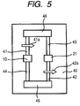
- Fig. 5 is a partial top plan view of the magnetic sensor with a structure different from that shown in Fig. 3 according to an embodiment of the application.
- Fig. 6 is a diagram illustrating a circuit configuration of the magnetic sensor shown in Fig. 3.
- Fig. 7 is a diagram illustrating a circuit configuration of the magnetic sensor shown in Fig. 5.
- a foldable cellular phone 1 has a first member 2 and a second member 3.
- the first member 2 is formed in a screen display and the second member 3 is formed in an operation body.
- a liquid crystal display, a receiver, and the like are provided on a surface of the first member 2 opposite to the second member 3.
- Buttons, a microphone, and the like are provided on a surface of the second member 3 opposite to the first member 2.
- the foldable cellular phone 1 is in a closed state.
- a magnet 5 is incorporated in the first member 2
- a magnetic sensor 5 is incorporated in the second member 3.
- the magnet 5 and the magnetic sensor 4 are disposed in locations in which the magnet 5 and the magnetic sensor 4 are opposite to each other (in a perpendicular direction with respect to the formation surface of the magnet 5 and the magnetic sensor 5).
- an external magnetic field ⁇ exerting from the magnet 5 is applied to the magnetic sensor 4, and then the external magnetic field ⁇ is detected by the magnetic sensor 4. In this manner, the closed state of the foldable cellular phone 1 is detected.
- the magnitude of the exterior magnetic field ⁇ applied to the magnetic sensor 4 gradually decreases as the first member 2 is separated far away from the second member 3, and finally becomes zero.
- the magnitude of the exterior magnetic field ⁇ applied to the magnetic sensor 4 becomes zero or decreases to a predetermined magnitude or less, the open state of the foldable cellular phone 1 is detected.
- a controller incorporated in the foldable cellular phone 1 controls a back light on a back side of the liquid crystal display or the operation button, for example, to emit light.
- the magnetic sensor 4 is mounted on a circuit board 6 incorporated in the second member 3.
- One magneto-resistive element 8 and one fixed resistor 9 are provided on an element base 7 of the magnetic sensor 4.
- terminal sections 10 and 11 are provided on both sides of the magneto-resistive element 8 in a length direction thereof.
- the terminal section 10 is electrically connected to an input terminal (power supply Vcc) 12 provided on the substrate 6 by a wire-bonding, a die-bonding, and the like (see Fig. 6).
- the terminal section 11 serves as a common terminal shared by the fixed resistor 9 and is electrically connected to an output terminal 22 on the substrate 6 by the wire-bonding, the die-bonding, and the like (see Fig. 6).
- the above-described terminal section 11 and a terminal section 21 are provided on both sides of the fixed resistor 9 in the length direction.
- the terminal section 21 is electrically connected to an earth terminal 13 on the circuit board 6 by the wire-bonding, the die-bonding, and the like (see Fig. 6).
- the magneto-resistive element 8 and the fixed resistor 9 are all formed in an elongated linear shape, but may be formed in a meander shape (S shape) and the like, for example.
- the magneto-resistive element 8 is sequentially laminated on an underlying layer 14, a seed layer 15, an antiferromagnetic layer 16, a fixed layer (a first magnetic layer) 17, a non-magnetic layer 18, a free layer (a magneto-sensitive layer, a second magnetic layer) 19, and a protection layer 20, in this order from a bottom surface.
- the underlying layer 14, for example, is formed of a non-magnetic material such as at least one atom selected from Ta, Hf, Nb, Zr, Ti, Mo, or W.
- the seed layer 15 is formed of NiFeCr, Cr, or the like.
- the antiferromagnetic layer 16 is formed of an antiferromagnetic material containing an atom ⁇ (where ⁇ is at least one atom of Pt, Pd, Ir, Rh, Ru, or Os) and Mn or that containing atoms ⁇ , ⁇ ' (where ⁇ ' is at least one atom selected from Ne, Ar, Kr, Xe, Be, B, C, N, Mg, Al, Si, P, Ti, V, Cr, Fe, Co, Ni, Cu, Zn, Ga, Ge, Zr, Nb, Mo, Ag, Cd, Sn, Hf, Ta, W, Re, Au, Pb, or a rare earth atom) and Mn.
- ⁇ is at least one atom of Pt, Pd, Ir, Rh, Ru, or Os
- Mn or that containing atoms ⁇ , ⁇ ' (where ⁇ ' is at least one atom selected from Ne, Ar, Kr, Xe, Be, B, C, N, Mg, Al,
- the antiferromagnetic layer 16 is formed of IrMn or PtMn.
- the fixed layer 17 and the free layer 19 are formed of magnetic materials such as a CoFe alloy, a NiFe alloy, a CoFeNi alloy, and the like.
- the non-magnetic layer 18 is formed of Cu or the like.
- the protection layer 20 is formed of Ta or the like.
- an exchange coupling magnetic field occurs in an interface between the antiferromagnetic layer 16 and the fixed layer 17 after a heat treatment process in a magnetic field, and thus a magnetization direction of the fixed layer 17 is fixed in one direction.
- a magnetization direction 17a of the fixed layer 17 is shown as an arrow direction in Fig. 3.
- the magnetization direction 17a is perpendicular to the length direction (a width direction of the element).
- the free layer 19 is opposing the fixed layer 17 via the non-magnetic layer 18, and the magnetization direction of the free layer 19 is not fixed in one direction. That is, the magnetization of the free layer 19 changes in accordance with the external magnetic field.
- the fixed resistor 9 is sequentially formed of the underlying layer 14, the seed layer 15, the antiferromagnetic layer 16, the first magnetic layer 17, the second magnetic layer 19, the non-magnetic layer 18, and the protection layer 20 in this order from a bottom surface.
- the first magnetic layer 17 and the second magnetic layer 19 in the fixed resistor 9 correspond to the fixed layer 17 and the free layer 19 in the magneto-resistive element 8, respectively. That is, an order of laminating the non-magnetic layer 18 and the free layer 19 in the magneto-resistive element 8 is changed each other in the fixed resistor 9. Materials of each common layer in the magnetoresistance 8 and the fixed resistor 9 are equal.
- the magneto-resistive element 8 when the magneto-resistive element 8 is sequentially formed of the underlying layer 14 (Ta), the seed layer 15 (NiFeCr), the antiferromagnetic layer 16 (IrMn), the fixed layer 17 (CoFe), the non-magnetic layer 18 (Cu), the free layer 19 (NiFe), and the protection layer 20 (Ta) from the bottom surface, the fixed resistor 9, for example, is sequentially formed of the underlying layer 14 (Ta), the seed layer 15 (NiFeCr), the antiferromagnetic layer 16 (IrMn), the first magnetic layer 17 (CoFe), the second magnetic layer 19 (NiFe), the non-magnetic layer 18 (Cu), and the protection layer 20 (Ta) from the bottom surface.
- the first magnetic layer 17 and the second layer 19 in the fixed resistor 9 are formed so as to be in contact.
- the antiferromagnetic layer 16 is formed in contact with the first magnetic layer 17 or the second magnetic layer 19.
- the antiferromagnetic layer 16, the first magnetic layer 17, and the second magnetic layer 19 are sequentially laminated in Fig. 4. Accordingly, when the heat treatment in a magnetic field is performed, the exchange coupling magnetic field (Hex) occurs in an interface between the antiferromagnetic layer 16 and the first magnetic layer 17 to fix the magnetization of the first magnetic layer 17 in one direction.
- Hex exchange coupling magnetic field
- the magnetization of the second magnetic layer 19 formed in contact with the first magnetic layer 17 is also fixed in the same direction as the magnetization direction of the first magnetic layer 17 due to an antiferromagnetic coupling which occurs between the second magnetic layer 19 and the first magnetic layer 17.
- the magnetization direction of the first magnetic layer 17 and the second magnetic layer 19 can be either equal or different from the magnetization direction 17a of the fixed layer 17 in the magneto-resistive element 8.
- the magnetization direction of the first magnetic layer 17 and the second magnetic layer 19 is the same as the magnetization direction 17a of the fixed layer 17. In the embodiment, the important point is that the magnetization direction of the first magnetic layer 17 and the second magnetic layer 19 is fixed.
- the order of laminating the second magnetic layer 19 and the non-magnetic layer 18 is changed each other in a manner different from the magneto-resistive element 8. In this manner, it is not necessary to change the order of laminating the magneto-resistive element 8. As a result, the magnetization direction of the magnetic layers 17 and 19 can be simply fixed, thereby making the manufacturing method simple.
- Figs. 3 and 6 for example, 5 V is applied from the input terminal (power supply Vcc), and then an output value (central potential) from the magnetic sensor 4 nearly becomes 2.5 V at a state with no-magnetic field according to the embodiment shown in Fig. 4.
- the exterior magnetic field ⁇ from the magnet 5 has an effect on the magneto-resistive element 8, and the magnitude variation changes a magnetization relation (magnetization state) between the free layer 19 and the fixed layer 17, thereby changing the resistance value of the magneto-resistive element 8 (which is called a magnetoresistance).
- the resistance value of the magneto-resistive element 9 is not changed in accordance with the exterior magnetic field ⁇ .
- the output value from the magnetic sensor 4 is changed, and then the output value is compared to the threshold voltage in a controller 30. For example, when the output value is higher than the threshold voltage, a switching signal to be switched-on is output.
- the foldable cellular phone 1 is open, and thus a operation of the back light is conducted.
- the switch becomes off, for example, the switching signal stops being output.
- the foldable cellular phone 1 is closed, the operation of the back light and the like stops.
- the magneto-resistive element 8 and the fixed resistor 9 have all the antiferromagnetic layer 16, the first magnetic layer 17, the non-magnetic layer 18, the second magnetic layer 19, and the protection layer 20 described above.
- the second magnetic layer 19 in the magneto-resistive element 8 serves as a free layer in which the magnetization direction is changed in accordance with variation of the exterior magnetic field.
- the second magnetic layer 19 in the fixed resistor 9 is formed in contact with the first magnetic layer 17, and thus the magnetization direction of the second magnetic layer 19 and the first magnetic layer 17 is fixed.
- the magneto-resistive element 8 serves as a variable resistor in which the magnetoresistance effect is influenced to change the resistance value in accordance with a change of the exterior magnetic field.
- the magnetoresistance effect is not influenced in accordance with the change of the exterior magnetic field and the resistance value is constant. Since the magneto-resistive element 8 and the fixed resistor 9 have all the antiferromagnetic layer 16, the first magnetic layer 17, the non-magnetic layer 18, the second magnetic layer 19, and the protection layer 20, an irregularity of the temperature coefficient of resistances (TCR) of the magneto-resistive element 8 and the fixed resistor 9 can be suppressed. As a result, an irregularity of the central potential with respect to a temperature change can be also suppressed, thereby realizing the magnetic sensor 4 to be stably operated.
- TCR temperature coefficient of resistances
- the constituent layers of the magneto-resistive element 8 completely accord with those of the fixed resistor 9. That is, since the underlying layer 14 and the seed layer 15 used in the magneto-resistive element 8 as well as the antiferromagnetic layer 16, the first magnetic layer 17, the non-magnetic layer 18, the second magnetic layer 19, and the protection layer 20 are also used in the fixed resistor 9, the irregularity of the temperature coefficient and the resistance value (state with non-magnetic field) of the magneto-resistive element 8 and the fixed resistor 9 can be more properly suppressed. Accordingly, the magnetic sensor 4 to be stably operated can be realized.
- the fixed layer 17 in the magneto-resistive element 8 can be a laminated ferri-structure in which a non-magnetic intermediate layer is interposed between two magnetic layers.
- the first magnetic layer 17 the two magnetic layers and the non-magnetic intermediate layer are provided in the fixed resistor 9. In this case, the first magnetic layer 17 and the fixed layer 17 may not be the same laminated ferri-structure.
- the fixed resistor 9 has the same laminated ferri-structure and same configuration elements and the magnetic layers are all fixed.
- the laminated ferri-structure includes the magnetic layer (CoFe), the non-magnetic intermediate layer (Ru), and the magnetic layer (CoFe)
- the fixed resistor 9 may be sequentially laminated of the magnetic layer (CoFe), the magnetic layer (CoFe), and the non-magnetic layer (Ru).
- the magnetization direction of all magnetic layers is simply fixed.
- the fixed resistor 9 is formed such that IrMn, CoFe, CoFe, CoFe, NiFe, Ru, and Cu can be laminated.
- the magneto-resistive element 8 and the fixed resistor 9 provided to the magnetic sensor 4 are mounted on the element base 7. Accordingly, the magnetic sensor 4 can decrease in size.
- the terminal section 11 provided on edges of magneto-resistive element 8 and the fixed resistor 9 can serves as a common terminal. Accordingly, the number of bonding between the magnetic sensor 4 and the circuit board 6 can decrease, thereby lowering the manufacturing cost rather than when the magneto-resistive element 8 and the fixed resistor 9 each are mounted on different element bases.
- the magnetization-controlling process of the magneto-resistive element 8 and the fixed resistor 9 can be simply performed.
- the magneto-resistive element 8 and the fixed resistor 9 each are mounted on the different element bases, the irregularity of the temperature coefficient of the magneto-resistive element 8 and the fixed resistor 9 can be suppressed.
- a precision of a high-location determination is not required and an irregularity of the detection precision can be suppressed rather than when the magneto-resistive element is formed on the same element base in the related art.
- the magneto-resistive element 8 and the fixed resistor 9 are formed on the same element base 7 in terms of a decrease in size of the magnetic sensor 4.
- a bridge circuit (half-bridge circuit) provided with each of the magneto-resistive element 8 and the fixed resistor 9 on the element base 7 is configured, but as shown in Figs. 5 and 7, a bridge circuit (full-bridge circuit) provided with two magneto-resistive elements 41 and 42 and two fixed resistors 43 and 44 on the element base 40 can be configured.
- magnetization directions 41a and 42a of the fixed layers in the magneto-resistive elements 41 and 42 can be equal.
- the magneto-resistive element 41 and the fixed resistor 43 can be connected to a common terminal (first output terminal) 46 and the magneto-resistive element 42 and the fixed resistor 44 can be connected to a common terminal (second output terminal) 45.
- the output can increase, thereby realizing the magnetic sensor 4 to be more stably operated.
- FIG. 8 to 13 are process diagrams illustrating the method of manufacturing the magnetic sensor 4 shown in Fig. 4, each of which corresponds to a partial sectional view of processes performed during the manufacturing process.
- a laminated body 52 is sequentially formed of the underlying layer 14, the antiferromagnetic layer 16, the fixed layer (first magnetic layer) 17, the non-magnetic layer 8, the free layer (second magnetic layer) 19, and the protection layer 20 from bottom on an entire substrate 50.
- the materials of each layer are described above and so see the above-description.
- a lift-off resist layer 51 is provided on the part which will become the magneto-resistive element 8.
- a width and length of the lift-off resist layer 51 are made longer than those of the magneto-resistive element 8.
- a part of the laminated body 52 without covering of the lift-off resist layer 51 is removed by the ion milling process and the like.
- a laminated body 53 is sequentially formed of the underlying layer 14, the seed layer 15, the antiferromagnetic layer 16, the fixed layer (first magnetic layer) 17, the second magnetic layer 19, the non-magnetic layer 8, and the protection layer 20 from bottom on the substrate 50 in which the laminated body 52 is removed.
- the materials of each layer are made the same as those of each layer common to the laminated body 52.
- the film thickness of each layer in the laminated body 53 is the same as that each layer common to the laminated body 52.
- a laminated body of layered structure similarly to the laminated body 53 is also laminated above the lift-off resist layer 51. Sequentially, the lift-off resist layer 51 is removed.
- the exchange coupling magnetic field (Hex) is arisen between the antiferromagnetic layer 16 and the fixed layer 17 constituting the laminated bodies 52 and 53 by performing the heat treatment process in a magnetic field.
- the fixed layer 17 of the laminated body 52 and the first magnetic layer 17 of the laminated body 53 are all magnetized in the same fixed direction.
- the heat treatment can be performed other than the above-time. At least, the heat treatment process needs only to be performed before a process representing Fig. 13 in which each element is cut out from the substrate 50. Since the heat treatment process in a magnetic field is performed on all the laminated bodies 52 and 53 formed on the substrate 50, the heat treatment process in a magnetic field can be simply performed.
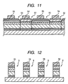
- a resist layer 54 with a pattern of the magneto-resistive element 8 is provided on the laminated body 52 and a resist layer 55 with a pattern of the fixed resistor 9 is provided on the laminated body 53.
- the patterns of the resist layers 54 and 55 are formed by the exposure and development processes.
- the left laminated body 52 and the left laminated body 53 serve as the magneto-resistive element 8 and the fixed resistor 9, respectively.
- each element base 7 is cut out from the substrate 50 (where each element base 7 is cut along the dashed-dotted line shown in Fig. 13). In this manner, a plurality of magnetic sensors 4 can be obtained from the substrate 50.
- the layers from bottom to the fixed layer 17 are common in the magneto-resistive element 8 and the fixed resistance 9, the layers from bottom to the fixed layer 17 are formed on the entire surface of the substrate 50, and then parts in which the fixed resistor 9 is formed are covered with the resist layer and the like. Sequentially, the non-magnetic layer 18, the free layer 19, and the protection layer 20 constituting the magneto-resistive element 8 are sequentially laminated on a part of the fixed layer 17 out of the covered part with the resist layer, before the resist layer is removed.
- the resist layer is covered on the magneto-resistive element 8, the magnetic layer 19, the non-magnetic layer 18, and the protection layer 20 constituting the fixed resistor 9 are sequentially laminated on the fixed layer 17 on which the resist layer is not covered, and the resist layer is removed similarly to the processes after Fig. 11.
- the above-described method can also form the magneto-resistive element 8 and the fixed resistor 9 on the substrate 50, but after the fixed layer 17 is formed, the magneto-resistive element 8 and the fixed resistor 9 suffer from excessive exposure to the atmosphere in order to provide the resist layer, thereby degrading the fixed layer 17. Accordingly, as shown in Figs. 8 to 10, it is preferable that the laminated body 52 constituting the magneto-resistive element 8 and the laminated body 53 constituting the fixed resistor 9 each are laminated such that degradation of the layers can be prevented.
- the magnet 5 is not included as the constituent of the magnetic sensor 4, but can be included as the constituent of the magnetic sensor 4.
- the magneto-resistive element 8 is sequentially formed of the antiferromagnetic layer 16, the fixed layer 17, the non-magnetic layer 18, and the free layer 19 from the bottom surface, but can be sequentially formed of the free layer 19, the non-magnetic layer 18, the fixed layer 17, and the antiferromagnetic layer 16.
- the fixed resistor 9 can be sequentially formed as shown in Fig. 4 and can be sequentially formed of the non-magnetic layer 18, the free layer 19, the fixed layer 17, and the antiferromagnetic layer 16.
- the underlying layer 14 and the seed layer 15 shown in Fig. 4 are optionally formed and are not necessarily provided.
- the magnetic sensor 4 is used for detecting the open and closed states of the foldable cellular phone 1, but can be also used for detecting the open and closed states of the game console.
- the magnetic sensor 4 shown in Fig. 1 outputs an ON/OFF signal on the basis of magnitude of the exterior magnetic field ⁇ from the magnet 5, but can also output the ON/OFF signal on the basis of variation of polarity of the magnet 5, or the magnetic sensor 4 can be used as a sensor for detecting a rotational angle such as a throttle position sensor or a geomagnetic sensor (direction sensor).
- the application provides a magnetic sensor which can suppress an irregularity of a central potential due to a change in a temperature, decrease size of the sensor, and lower the manufacturing cost of the sensor.
- a magneto-resistive element 8 and fixed resistor 9 are provided on an element base 7 and have the same configuration elements.
- a second magnetic layer 19 and non-magnetic layer 18 in the fixed resistor 9 are reversely laminated on each other in a manner different from the magneto-resistive element 8, and the second magnetic layer 19 is formed in contact with the first magnetic layer 17, thereby fixing the magnetization directions of the first magnetic layer 17 and the second magnetic layer 19 to the same direction. In this manner, the irregularity of the temperature coefficient between the magneto-resistive element 8 and the fixed resistor 9 is suppressed, and the irregularity of the central potential due to the change in the temperature is suppressed.
Landscapes
- Physics & Mathematics (AREA)
- Condensed Matter Physics & Semiconductors (AREA)
- General Physics & Mathematics (AREA)
- Measuring Magnetic Variables (AREA)
- Hall/Mr Elements (AREA)
Abstract
Description
- The application relates to a non-contact magnetic sensor for detecting the open and closed states of a foldable cellular phone, and more particularly, to a magnetic sensor which can suppress irregularity of a central potential due to a change in a temperature, decrease the size and manufacturing cost of the sensor.
- A method of assembling a magnetic sensor is disclosed in
JP-A-2003-066127 JP-A-2003-066127 JP-A-2003-066127 - Fig. 14 is a partial top plan view of the known magnetic sensor. As shown in Fig. 14, the magneto-
resistive elements element bases -
Terminal sections resistive elements terminal sections terminal section 66 on acircuit board 65 by wire bonding, for example. - In the magnetic sensor, for example in order to detect a change in a central potential, the fixed layers in the magneto-
resistive elements - The magnetic sensor shown in Fig. 14 is used for detecting the open and closed states of a mobile phone, for example. That is, a magnet is provided on a first member (for example, a member in which a display screen is mounted) of the mobile phone and the magnetic sensor shown in Fig. 14 is incorporated in a second member (for example, an operation member). The magnitude of an exterior magnetic field from the magnet influencing on the magneto-
resistive elements resistive elements resistive elements - Since the magneto-
resistive elements resistive elements JP-A-2003-066127 element bases resistive elements - However, it is considerably difficult to match the directions of the
element bases - Additionally, a combination of a plurality of element bases, as depicted in Fig. 14, bring too large size to the magnetic sensor. As the number of bonding positions between the
terminal sections resistive elements terminal section 66 of thecircuit board 65 increases, the manufacturing cost increases accordingly. - Meanwhile, when a bridge circuit is configured by combining the magneto-resistive element with the fixed resistor, for example, the magneto-resistive element and the fixed resistor can be formed on the same element base, thereby solving the above problems.
- However, since the materials of the magneto-resistive element and the fixed resistor are different from each other, temperature coefficients of resistance (TCR) thereof are different from each other. As a result, as the temperature varies, a central voltage becomes unbalanced and the detection precision is lowered, thereby causing a false operation.
- The application is made to solve the above problems, and it is an object of the application to provide a magnetic sensor which can suppress irregularity of a central potential due to a change in a temperature and decrease the size and manufacturing cost of the magnetic sensor.
- According to an aspect of the application, a magnetic sensor includes at least one magneto-resistive element and at least one fixed resistor, where the magneto-resistive element and the fixed resistor all have an antiferromagnetic layer, a plurality of magnetic layers, a non-magnetic layer, and a protection layer serving as the uppermost layer;
wherein the magneto-resistive element constitutes - a fixed layer having at least the one magnetic layer with a fixed magnetization direction,
- a magneto-sensitive layer having the other magnetic layers with the magnetization directions variable by an exterior magnetic field,
- the non-magnetic layer being interposed between the fixed layers and the magneto-sensitive layer, and
- the antiferromagnetic layer being formed in contact with a surface opposite to the surface in which the non-magnetic of the fixed layer is formed; and
- wherein in the fixed resistor, at least one magnetic layer is formed in contact with the antiferromagnetic layer and the magnetization directions of all the magnetic layers are fixed.
- As described above, in the above-mentioned aspect of the application, the antiferromagnetic layer, the plurality of magnetic layers, the non-magnetic layer, and the protection layer are used as a constituent layer of the magneto-resistive element and the fixed resistor. By changing the order of laminating the constituent layer of the magneto-resistive element and the fixed resistor, the magneto-resistive element serves as a variable resistor in which the magnetoresistance effect is properly exhibited on the basis of a change in the exterior magnetic field, thereby changing the resistance value. On the other hand, since the magnetization directions of all the magnetic layers are fixed in a regular direction, the magnetoresistance effect in the fixed resistor is not exhibited even with the change in the exterior magnetic field in a manner different from the magneto-resistive element.
- As described above, according to the application, since the magneto-resistive element and the fixed resistor all have the antiferromagnetic layer, the plurality of magnetic layers, the non-magnetic layer, and the protection layer, it is possible to suppress the irregularity of the temperature coefficients in the magneto-resistive element and the fixed resistor, compared with the case of the known magnetic sensor. Accordingly, it is possible to stably operate the magnetic sensor even with the change in the temperature.
- In the above-mentioned aspect of the application, it is desirable that a first magnetic layer corresponding to the fixed layer and a second magnetic layer corresponding to a free layer are laminated on the fixed resistor, and the antiferromagnetic layer is formed in contact with the laminated magnetic layers to fix the magnetization directions of the laminated magnetic layers in one direction. Specifically, it is desirable that the first magnetic layer is formed in contact with the antiferromagnetic layer, and the second magnetic layer and the non-magnetic layer are reversely laminated on each other in a manner different from the magneto-resistive element, and the second magnetic layer is formed in contact with a surface opposite to the surface where the antiferromagnetic layer of the first magnetic layer is formed, thereby fixing the magnetization direction of the second magnetic layer to the same direction as the first magnetic layer.
- In this manner, it is possible to fix the magnetization directions of all the magnetic layers with a simple configuration.
- In the above-mentioned aspect of the application, it is desirable that the magneto-resistive element and the fixed resistor are formed on the same element base. In this manner, it is possible to further downsize the magnetic sensor and decrease the number of bonding and the like, thereby decreasing the manufacturing cost.
- In the above-mentioned aspect of the application, it is desirable that the magneto-resistive element and the fixed resistor have the same layer configuration. For example, besides the antiferromagnetic layer, the fixed layer, the non-magnetic layer, magneto-sensitive layer, and the protection layer, a seed layer for improving crystallinity may be provided in the magneto-resistive element. When the seed layer is also provided in the fixed resistor, by forming the magneto-resistive element with the same constituent layers as that of the fixed resistor, the irregularity of the temperature coefficients in the magneto-resistive element and the fixed resistor may be more effectively lowered (or most preferably, the temperature coefficients may become equal to each other). Accordingly, it is possible to obtain a magnetic sensor capable of stably operating even with the change in the temperature.
- According to the magnetic sensor of the above-mentioned aspect of the application, it is possible to suppress the irregularity of the central potential level even with the change in the temperature and decrease the size and manufacturing cost of the magnetic sensor.
-
- Fig. 1 is a partially schematic diagram showing a foldable cellular phone with a built-in magnetic sensor according to an embodiment of the application (closed state).
- Fig. 2 is a partially schematic diagram showing a foldable cellular phone with a built-in magnetic sensor according to the embodiment of the application (open state).
- Fig. 3 is a partial top plan view of the magnetic sensor according to an embodiment of the application.
- Fig. 4 is a partial top plan view of the magnetic sensor taken along a line A-A of Fig. 3.
- Fig. 5 is a partial top plan view of the magnetic sensor with a structure different from that shown in Fig. 3 according to an embodiment of the application.
- Fig. 6 is a diagram illustrating a circuit configuration of the magnetic sensor shown in Fig. 3.
- Fig. 7 is a diagram illustrating a circuit configuration of the magnetic sensor shown in Fig. 5.
- Fig. 8 is a process diagram illustrating a method of manufacturing the magnetic sensor according to an embodiment of the application (partially top plan view).
- Fig. 9 is a process diagram illustrating processes performed after the processes illustrated in Fig. 8 (partially top plan view).
- Fig. 10 is a process diagram illustrating processes performed after the processes illustrated in Fig. 9 (partially top plan view).
- Fig. 11 is a process diagram illustrating processes performed after the processes illustrated in Fig. 10 (partially top plan view).
- Fig. 12 is a process diagram illustrating processes performed after the processes illustrated in Fig. 11 (partially top plan view).
- Fig. 13 is a process diagram illustrating processes performed after the processes illustrated in Fig. 12 (partially top plan view).
- Fig. 14 is a partially top plan view of a magnetic sensor known in the art.
- Figs. 1 and 2 are partial schematic diagrams showing a foldable cellular phone with a built-in a magnetic sensor according to an embodiment of the application. Fig. 3 is a partial top plan view of the magnetic sensor according to an embodiment of the application. Fig. 4 is a partial top plan view of the magnetic sensor taken along a line A-A of Fig. 3. Fig. 5 is a partial top plan view of the magnetic sensor with a structure different from that shown in Fig. 3 according to an embodiment of the application. Fig. 6 is a diagram illustrating a circuit configuration of the magnetic sensor shown in Fig. 3. Fig. 7 is a diagram illustrating a circuit configuration of the magnetic sensor shown in Fig. 5.
- As shown in Fig. 1, a foldable cellular phone 1 has a
first member 2 and asecond member 3. Thefirst member 2 is formed in a screen display and thesecond member 3 is formed in an operation body. A liquid crystal display, a receiver, and the like are provided on a surface of thefirst member 2 opposite to thesecond member 3. Buttons, a microphone, and the like are provided on a surface of thesecond member 3 opposite to thefirst member 2. As shown in Fig. 1, the foldable cellular phone 1 is in a closed state. As shown in Fig. 1, a magnet 5 is incorporated in thefirst member 2, and a magnetic sensor 5 is incorporated in thesecond member 3. When the foldable cellular phone 1 is in the closed state as shown in Fig. 1, the magnet 5 and themagnetic sensor 4 are disposed in locations in which the magnet 5 and themagnetic sensor 4 are opposite to each other (in a perpendicular direction with respect to the formation surface of the magnet 5 and the magnetic sensor 5). - As shown in Fig. 1, an external magnetic field φ exerting from the magnet 5 is applied to the
magnetic sensor 4, and then the external magnetic field φ is detected by themagnetic sensor 4. In this manner, the closed state of the foldable cellular phone 1 is detected. - On the other hand, when the foldable cellular phone is opened as shown in Fig. 2, the magnitude of the exterior magnetic field φ applied to the
magnetic sensor 4 gradually decreases as thefirst member 2 is separated far away from thesecond member 3, and finally becomes zero. When the magnitude of the exterior magnetic field φ applied to themagnetic sensor 4 becomes zero or decreases to a predetermined magnitude or less, the open state of the foldable cellular phone 1 is detected. Then, a controller incorporated in the foldable cellular phone 1 controls a back light on a back side of the liquid crystal display or the operation button, for example, to emit light. - As shown in Fig. 3, the
magnetic sensor 4 according to the embodiment is mounted on acircuit board 6 incorporated in thesecond member 3. One magneto-resistive element 8 and one fixedresistor 9 are provided on anelement base 7 of themagnetic sensor 4. As shown in Fig. 3,terminal sections resistive element 8 in a length direction thereof. For example, theterminal section 10 is electrically connected to an input terminal (power supply Vcc) 12 provided on thesubstrate 6 by a wire-bonding, a die-bonding, and the like (see Fig. 6). Theterminal section 11 serves as a common terminal shared by the fixedresistor 9 and is electrically connected to anoutput terminal 22 on thesubstrate 6 by the wire-bonding, the die-bonding, and the like (see Fig. 6). - As shown in Fig. 3, the above-described
terminal section 11 and aterminal section 21 are provided on both sides of the fixedresistor 9 in the length direction. Theterminal section 21 is electrically connected to anearth terminal 13 on thecircuit board 6 by the wire-bonding, the die-bonding, and the like (see Fig. 6). - As shown in Fig. 3, the magneto-
resistive element 8 and the fixedresistor 9 are all formed in an elongated linear shape, but may be formed in a meander shape (S shape) and the like, for example. - As shown in Fig. 4, the magneto-
resistive element 8 is sequentially laminated on anunderlying layer 14, aseed layer 15, anantiferromagnetic layer 16, a fixed layer (a first magnetic layer) 17, anon-magnetic layer 18, a free layer (a magneto-sensitive layer, a second magnetic layer) 19, and aprotection layer 20, in this order from a bottom surface. Theunderlying layer 14, for example, is formed of a non-magnetic material such as at least one atom selected from Ta, Hf, Nb, Zr, Ti, Mo, or W. Theseed layer 15 is formed of NiFeCr, Cr, or the like. Theantiferromagnetic layer 16 is formed of an antiferromagnetic material containing an atom α (where α is at least one atom of Pt, Pd, Ir, Rh, Ru, or Os) and Mn or that containing atoms α, α' (where α' is at least one atom selected from Ne, Ar, Kr, Xe, Be, B, C, N, Mg, Al, Si, P, Ti, V, Cr, Fe, Co, Ni, Cu, Zn, Ga, Ge, Zr, Nb, Mo, Ag, Cd, Sn, Hf, Ta, W, Re, Au, Pb, or a rare earth atom) and Mn. For example, theantiferromagnetic layer 16 is formed of IrMn or PtMn. The fixedlayer 17 and thefree layer 19 are formed of magnetic materials such as a CoFe alloy, a NiFe alloy, a CoFeNi alloy, and the like. Thenon-magnetic layer 18 is formed of Cu or the like. Theprotection layer 20 is formed of Ta or the like. - Since the
antiferromagnetic layer 16 and the fixedlayer 17 in the magneto-resistive element 8 are formed in contact, an exchange coupling magnetic field (Hex) occurs in an interface between theantiferromagnetic layer 16 and the fixedlayer 17 after a heat treatment process in a magnetic field, and thus a magnetization direction of the fixedlayer 17 is fixed in one direction. Amagnetization direction 17a of the fixedlayer 17 is shown as an arrow direction in Fig. 3. Themagnetization direction 17a is perpendicular to the length direction (a width direction of the element). On the other hand, thefree layer 19 is opposing the fixedlayer 17 via thenon-magnetic layer 18, and the magnetization direction of thefree layer 19 is not fixed in one direction. That is, the magnetization of thefree layer 19 changes in accordance with the external magnetic field. - As shown in Fig. 4, the fixed
resistor 9 is sequentially formed of theunderlying layer 14, theseed layer 15, theantiferromagnetic layer 16, the firstmagnetic layer 17, the secondmagnetic layer 19, thenon-magnetic layer 18, and theprotection layer 20 in this order from a bottom surface. The firstmagnetic layer 17 and the secondmagnetic layer 19 in the fixedresistor 9 correspond to the fixedlayer 17 and thefree layer 19 in the magneto-resistive element 8, respectively. That is, an order of laminating thenon-magnetic layer 18 and thefree layer 19 in the magneto-resistive element 8 is changed each other in the fixedresistor 9. Materials of each common layer in themagnetoresistance 8 and the fixedresistor 9 are equal. For example, when the magneto-resistive element 8 is sequentially formed of the underlying layer 14 (Ta), the seed layer 15 (NiFeCr), the antiferromagnetic layer 16 (IrMn), the fixed layer 17 (CoFe), the non-magnetic layer 18 (Cu), the free layer 19 (NiFe), and the protection layer 20 (Ta) from the bottom surface, the fixedresistor 9, for example, is sequentially formed of the underlying layer 14 (Ta), the seed layer 15 (NiFeCr), the antiferromagnetic layer 16 (IrMn), the first magnetic layer 17 (CoFe), the second magnetic layer 19 (NiFe), the non-magnetic layer 18 (Cu), and the protection layer 20 (Ta) from the bottom surface. According to the embodiment shown in Fig. 4, the firstmagnetic layer 17 and thesecond layer 19 in the fixedresistor 9 are formed so as to be in contact. Theantiferromagnetic layer 16 is formed in contact with the firstmagnetic layer 17 or the secondmagnetic layer 19. Theantiferromagnetic layer 16, the firstmagnetic layer 17, and the secondmagnetic layer 19 are sequentially laminated in Fig. 4. Accordingly, when the heat treatment in a magnetic field is performed, the exchange coupling magnetic field (Hex) occurs in an interface between theantiferromagnetic layer 16 and the firstmagnetic layer 17 to fix the magnetization of the firstmagnetic layer 17 in one direction. However, the magnetization of the secondmagnetic layer 19 formed in contact with the firstmagnetic layer 17 is also fixed in the same direction as the magnetization direction of the firstmagnetic layer 17 due to an antiferromagnetic coupling which occurs between the secondmagnetic layer 19 and the firstmagnetic layer 17. The magnetization direction of the firstmagnetic layer 17 and the secondmagnetic layer 19 can be either equal or different from themagnetization direction 17a of the fixedlayer 17 in the magneto-resistive element 8. However, since it is easier to control the magnetic field during the manufacturing process, it is preferable that the magnetization direction of the firstmagnetic layer 17 and the secondmagnetic layer 19 is the same as themagnetization direction 17a of the fixedlayer 17. In the embodiment, the important point is that the magnetization direction of the firstmagnetic layer 17 and the secondmagnetic layer 19 is fixed. Accordingly, it is not necessary to sequentially laminate theantiferromagnetic layer 16, the firstmagnetic layer 17, and the secondmagnetic layer 19, but it is possible to sequentially laminate the firstmagnetic layer 17, theantiferromagnetic layer 16, the secondmagnetic layer 19, and thenon-magnetic layer 18, ..., and the like. However, as shown in Fig. 4, the order of laminating the secondmagnetic layer 19 and thenon-magnetic layer 18 is changed each other in a manner different from the magneto-resistive element 8. In this manner, it is not necessary to change the order of laminating the magneto-resistive element 8. As a result, the magnetization direction of themagnetic layers - As shown in Figs. 3 and 6, for example, 5 V is applied from the input terminal (power supply Vcc), and then an output value (central potential) from the
magnetic sensor 4 nearly becomes 2.5 V at a state with no-magnetic field according to the embodiment shown in Fig. 4. The exterior magnetic field φ from the magnet 5 has an effect on the magneto-resistive element 8, and the magnitude variation changes a magnetization relation (magnetization state) between thefree layer 19 and the fixedlayer 17, thereby changing the resistance value of the magneto-resistive element 8 (which is called a magnetoresistance). However, the resistance value of the magneto-resistive element 9 is not changed in accordance with the exterior magnetic field φ. The output value from themagnetic sensor 4 is changed, and then the output value is compared to the threshold voltage in acontroller 30. For example, when the output value is higher than the threshold voltage, a switching signal to be switched-on is output. The foldable cellular phone 1 is open, and thus a operation of the back light is conducted. On the other hand, when the output value is lower than the threshold, the switch becomes off, for example, the switching signal stops being output. The foldable cellular phone 1 is closed, the operation of the back light and the like stops. - According to the embodiment, the magneto-
resistive element 8 and the fixedresistor 9 have all theantiferromagnetic layer 16, the firstmagnetic layer 17, thenon-magnetic layer 18, the secondmagnetic layer 19, and theprotection layer 20 described above. The secondmagnetic layer 19 in the magneto-resistive element 8 serves as a free layer in which the magnetization direction is changed in accordance with variation of the exterior magnetic field. The secondmagnetic layer 19 in the fixedresistor 9 is formed in contact with the firstmagnetic layer 17, and thus the magnetization direction of the secondmagnetic layer 19 and the firstmagnetic layer 17 is fixed. - The magneto-
resistive element 8 serves as a variable resistor in which the magnetoresistance effect is influenced to change the resistance value in accordance with a change of the exterior magnetic field. On the other hand, as for the fixedresistor 9, the magnetoresistance effect is not influenced in accordance with the change of the exterior magnetic field and the resistance value is constant. Since the magneto-resistive element 8 and the fixedresistor 9 have all theantiferromagnetic layer 16, the firstmagnetic layer 17, thenon-magnetic layer 18, the secondmagnetic layer 19, and theprotection layer 20, an irregularity of the temperature coefficient of resistances (TCR) of the magneto-resistive element 8 and the fixedresistor 9 can be suppressed. As a result, an irregularity of the central potential with respect to a temperature change can be also suppressed, thereby realizing themagnetic sensor 4 to be stably operated. - In particular, according to the embodiment shown in Fig. 4, the constituent layers of the magneto-
resistive element 8 completely accord with those of the fixedresistor 9. That is, since theunderlying layer 14 and theseed layer 15 used in the magneto-resistive element 8 as well as theantiferromagnetic layer 16, the firstmagnetic layer 17, thenon-magnetic layer 18, the secondmagnetic layer 19, and theprotection layer 20 are also used in the fixedresistor 9, the irregularity of the temperature coefficient and the resistance value (state with non-magnetic field) of the magneto-resistive element 8 and the fixedresistor 9 can be more properly suppressed. Accordingly, themagnetic sensor 4 to be stably operated can be realized. In order to approximate the temperature coefficient of the fixedresistor 9 to the resistance value (the most preferably to accord with each other), it is required that the film thickness of each common layer in the magneto-resistive element 8 and the fixedresistor 9 is made equal. Additionally, the fixedlayer 17 in the magneto-resistive element 8, for example, can be a laminated ferri-structure in which a non-magnetic intermediate layer is interposed between two magnetic layers. As the firstmagnetic layer 17, the two magnetic layers and the non-magnetic intermediate layer are provided in the fixedresistor 9. In this case, the firstmagnetic layer 17 and the fixedlayer 17 may not be the same laminated ferri-structure. What is important is that the fixedresistor 9 has the same laminated ferri-structure and same configuration elements and the magnetic layers are all fixed. For example, when the laminated ferri-structure includes the magnetic layer (CoFe), the non-magnetic intermediate layer (Ru), and the magnetic layer (CoFe), the fixedresistor 9 may be sequentially laminated of the magnetic layer (CoFe), the magnetic layer (CoFe), and the non-magnetic layer (Ru). For example, when all magnetic layers are sequentially formed on theantiferromagnetic layer 16 and the other non-magnetic layer is formed on the magnetic layer in the fixedresistor 9, the magnetization direction of all magnetic layers is simply fixed. For example, when the magneto-resistive element 8 is formed such that the antiferromagnetic layer 16 (IrMn), the fixed layers 17 (CoFe, Ru, and CoFe), the non-magnetic layer 18 (Cu), and the free layers 19 (CoFe and NiFe) are sequentially laminated, the fixedresistor 9, for example, is formed such that IrMn, CoFe, CoFe, CoFe, NiFe, Ru, and Cu can be laminated. As a result, all magnetic direction of CoFe, CoFe, CoFe, and NiFe, which are a plurality of magnetic layers, can be properly fixed. - Additionally, as shown in Figs. 3 and 4, the magneto-
resistive element 8 and the fixedresistor 9 provided to themagnetic sensor 4 are mounted on theelement base 7. Accordingly, themagnetic sensor 4 can decrease in size. By forming the magneto-resistive element 8 and the fixedresistor 9 on thesame element base 7, theterminal section 11 provided on edges of magneto-resistive element 8 and the fixedresistor 9 can serves as a common terminal. Accordingly, the number of bonding between themagnetic sensor 4 and thecircuit board 6 can decrease, thereby lowering the manufacturing cost rather than when the magneto-resistive element 8 and the fixedresistor 9 each are mounted on different element bases. Further, since the magneto-resistive element 8 and the fixedresistor 9 are formed on thesame element base 7, the magnetization-controlling process of the magneto-resistive element 8 and the fixedresistor 9 can be simply performed. - According to the embodiment, even when the magneto-
resistive element 8 and the fixedresistor 9 each are mounted on the different element bases, the irregularity of the temperature coefficient of the magneto-resistive element 8 and the fixedresistor 9 can be suppressed. On the other hand, a precision of a high-location determination is not required and an irregularity of the detection precision can be suppressed rather than when the magneto-resistive element is formed on the same element base in the related art. However, it is preferable that the magneto-resistive element 8 and the fixedresistor 9 are formed on thesame element base 7 in terms of a decrease in size of themagnetic sensor 4. - According to the embodiment shown in Figs. 3 and 4, a bridge circuit (half-bridge circuit) provided with each of the magneto-
resistive element 8 and the fixedresistor 9 on theelement base 7 is configured, but as shown in Figs. 5 and 7, a bridge circuit (full-bridge circuit) provided with two magneto-resistive elements resistors element base 40 can be configured. As shown in Fig. 5,magnetization directions resistive elements resistive element 41 and the fixedresistor 43 can be connected to a common terminal (first output terminal) 46 and the magneto-resistive element 42 and the fixedresistor 44 can be connected to a common terminal (second output terminal) 45. - As shown in Figs. 5 and 7, by configuring the full-bridge circuit, the output can increase, thereby realizing the
magnetic sensor 4 to be more stably operated. - A method of manufacturing the
magnetic sensor 4 shown in Fig. 4 will be described below. Figs. 8 to 13 are process diagrams illustrating the method of manufacturing themagnetic sensor 4 shown in Fig. 4, each of which corresponds to a partial sectional view of processes performed during the manufacturing process. - In a process represented in Fig. 8, a
laminated body 52 is sequentially formed of theunderlying layer 14, theantiferromagnetic layer 16, the fixed layer (first magnetic layer) 17, thenon-magnetic layer 8, the free layer (second magnetic layer) 19, and theprotection layer 20 from bottom on anentire substrate 50. The materials of each layer are described above and so see the above-description. - Next, in a process represented in Fig. 9, as the
protection layer 20, a lift-off resistlayer 51 is provided on the part which will become the magneto-resistive element 8. A width and length of the lift-off resistlayer 51 are made longer than those of the magneto-resistive element 8. A part of thelaminated body 52 without covering of the lift-off resistlayer 51 is removed by the ion milling process and the like. - Next, in a process represented in Fig. 10, a
laminated body 53 is sequentially formed of theunderlying layer 14, theseed layer 15, theantiferromagnetic layer 16, the fixed layer (first magnetic layer) 17, the secondmagnetic layer 19, thenon-magnetic layer 8, and theprotection layer 20 from bottom on thesubstrate 50 in which thelaminated body 52 is removed. The materials of each layer are made the same as those of each layer common to thelaminated body 52. The film thickness of each layer in thelaminated body 53 is the same as that each layer common to thelaminated body 52. A laminated body of layered structure similarly to thelaminated body 53 is also laminated above the lift-off resistlayer 51. Sequentially, the lift-off resistlayer 51 is removed. - After the
laminated body 53 is formed, the exchange coupling magnetic field (Hex) is arisen between theantiferromagnetic layer 16 and the fixedlayer 17 constituting thelaminated bodies layer 17 of thelaminated body 52 and the firstmagnetic layer 17 of thelaminated body 53 are all magnetized in the same fixed direction. The heat treatment can be performed other than the above-time. At least, the heat treatment process needs only to be performed before a process representing Fig. 13 in which each element is cut out from thesubstrate 50. Since the heat treatment process in a magnetic field is performed on all thelaminated bodies substrate 50, the heat treatment process in a magnetic field can be simply performed. - In a process represented in Fig. 11, a resist
layer 54 with a pattern of the magneto-resistive element 8 is provided on thelaminated body 52 and a resistlayer 55 with a pattern of the fixedresistor 9 is provided on thelaminated body 53. The patterns of the resistlayers - When a part of the
laminated bodies layers laminated body 52 and the leftlaminated body 53 serve as the magneto-resistive element 8 and the fixedresistor 9, respectively. - Additionally, in a process represented in Fig. 13, each
element base 7 is cut out from the substrate 50 (where eachelement base 7 is cut along the dashed-dotted line shown in Fig. 13). In this manner, a plurality ofmagnetic sensors 4 can be obtained from thesubstrate 50. - For example, since the layers from bottom to the fixed
layer 17 are common in the magneto-resistive element 8 and the fixedresistance 9, the layers from bottom to the fixedlayer 17 are formed on the entire surface of thesubstrate 50, and then parts in which the fixedresistor 9 is formed are covered with the resist layer and the like. Sequentially, thenon-magnetic layer 18, thefree layer 19, and theprotection layer 20 constituting the magneto-resistive element 8 are sequentially laminated on a part of the fixedlayer 17 out of the covered part with the resist layer, before the resist layer is removed. The resist layer is covered on the magneto-resistive element 8, themagnetic layer 19, thenon-magnetic layer 18, and theprotection layer 20 constituting the fixedresistor 9 are sequentially laminated on the fixedlayer 17 on which the resist layer is not covered, and the resist layer is removed similarly to the processes after Fig. 11. The above-described method can also form the magneto-resistive element 8 and the fixedresistor 9 on thesubstrate 50, but after the fixedlayer 17 is formed, the magneto-resistive element 8 and the fixedresistor 9 suffer from excessive exposure to the atmosphere in order to provide the resist layer, thereby degrading the fixedlayer 17. Accordingly, as shown in Figs. 8 to 10, it is preferable that thelaminated body 52 constituting the magneto-resistive element 8 and thelaminated body 53 constituting the fixedresistor 9 each are laminated such that degradation of the layers can be prevented. - According to the embodiment, the magnet 5 is not included as the constituent of the
magnetic sensor 4, but can be included as the constituent of themagnetic sensor 4. - Additionally, according to the embodiment, the magneto-
resistive element 8 is sequentially formed of theantiferromagnetic layer 16, the fixedlayer 17, thenon-magnetic layer 18, and thefree layer 19 from the bottom surface, but can be sequentially formed of thefree layer 19, thenon-magnetic layer 18, the fixedlayer 17, and theantiferromagnetic layer 16. In this case, the fixedresistor 9 can be sequentially formed as shown in Fig. 4 and can be sequentially formed of thenon-magnetic layer 18, thefree layer 19, the fixedlayer 17, and theantiferromagnetic layer 16. Theunderlying layer 14 and theseed layer 15 shown in Fig. 4 are optionally formed and are not necessarily provided. - Further, the
magnetic sensor 4 according to the embodiment is used for detecting the open and closed states of the foldable cellular phone 1, but can be also used for detecting the open and closed states of the game console. Themagnetic sensor 4 shown in Fig. 1 outputs an ON/OFF signal on the basis of magnitude of the exterior magnetic field φ from the magnet 5, but can also output the ON/OFF signal on the basis of variation of polarity of the magnet 5, or themagnetic sensor 4 can be used as a sensor for detecting a rotational angle such as a throttle position sensor or a geomagnetic sensor (direction sensor). - The application provides a magnetic sensor which can suppress an irregularity of a central potential due to a change in a temperature, decrease size of the sensor, and lower the manufacturing cost of the sensor. A magneto-
resistive element 8 and fixedresistor 9 are provided on anelement base 7 and have the same configuration elements. A secondmagnetic layer 19 andnon-magnetic layer 18 in the fixedresistor 9 are reversely laminated on each other in a manner different from the magneto-resistive element 8, and the secondmagnetic layer 19 is formed in contact with the firstmagnetic layer 17, thereby fixing the magnetization directions of the firstmagnetic layer 17 and the secondmagnetic layer 19 to the same direction. In this manner, the irregularity of the temperature coefficient between the magneto-resistive element 8 and the fixedresistor 9 is suppressed, and the irregularity of the central potential due to the change in the temperature is suppressed.
Claims (5)
- A magnetic sensor comprising;at least one magneto-resistive element; andat least one fixed resistor,wherein the magneto-resistive element and the fixed resistor all have an antiferromagnetic layer, a plurality of magnetic layers, a non-magnetic layer, and a protection layer serving as the uppermost layer;wherein the magneto-resistive element is provided with a fixed layer that has at least one magnetic layer and a magnetization direction thereof is fixed in one direction, and a magneto-sensitive layer which has the remaining magnetic layers and the magnetization direction thereof varies in accordance with an exterior magnetic field, the non-magnetic layer being interposed between the fixed layer and the magneto-sensitive layer, and the antiferromagnetic layer being formed in contact with a surface opposite to the surface where the non-magnetic of the fixed layer is formed; andwherein in the fixed resistor, at least one magnetic layer is formed in contact with the antiferromagnetic layer, and the magnetization directions of all the magnetic layers are fixed in one direction.
- The magnetic sensor according to Claim 1, wherein a first magnetic layer corresponding to the fixed layer and a second magnetic layer corresponding to a free layer are laminated on the fixed resistor, and the antiferromagnetic layer is formed in contact with the laminated magnetic layers to fix the magnetization directions of the laminated magnetic layers in one direction.
- The magnetic sensor according to Claim 2, wherein the first magnetic layer is formed in contact with the antiferromagnetic layer, and the second magnetic layer and the non-magnetic layer are reversely laminated on each other in a manner different from the magneto-resistive element, and the second magnetic layer is formed in contact with a surface opposite to the surface where the antiferromagnetic layer of the first magnetic layer is formed, thereby fixing the magnetization direction of the second magnetic layer to the same direction as the first magnetic layer.
- The magnetic sensor according to any of Claims 1 to 3, wherein the magneto-resistive element and the fixed resistor are formed on the same element base.
- The magnetic sensor according to any of Claims 1 to 4, wherein the magneto-resistive element and the fixed resistor have the same layer configuration.
Applications Claiming Priority (1)
| Application Number | Priority Date | Filing Date | Title |
|---|---|---|---|
| JP2006067737A JP4668818B2 (en) | 2006-03-13 | 2006-03-13 | Magnetic sensor |
Publications (3)
| Publication Number | Publication Date |
|---|---|
| EP1835298A2 true EP1835298A2 (en) | 2007-09-19 |
| EP1835298A3 EP1835298A3 (en) | 2010-07-28 |
| EP1835298B1 EP1835298B1 (en) | 2011-10-19 |
Family
ID=38110137
Family Applications (1)
| Application Number | Title | Priority Date | Filing Date |
|---|---|---|---|
| EP07004494A Active EP1835298B1 (en) | 2006-03-13 | 2007-03-05 | Bridge-circuited magnetic sensor having magneto-resistive element and fixed resistor with the same layer configuration |
Country Status (3)
| Country | Link |
|---|---|
| US (1) | US7336070B2 (en) |
| EP (1) | EP1835298B1 (en) |
| JP (1) | JP4668818B2 (en) |
Families Citing this family (9)
| Publication number | Priority date | Publication date | Assignee | Title |
|---|---|---|---|---|
| JP5007916B2 (en) * | 2006-03-28 | 2012-08-22 | 日立金属株式会社 | Magnetic sensor |
| WO2010143718A1 (en) | 2009-06-12 | 2010-12-16 | アルプス・グリーンデバイス株式会社 | Magnetic balance current sensor |
| CN102812376B (en) * | 2010-03-12 | 2016-02-10 | 阿尔卑斯电气株式会社 | Magnetic sensors and magnetically balanced current sensors using magnetic sensors |
| JPWO2011111494A1 (en) * | 2010-03-12 | 2013-06-27 | アルプス電気株式会社 | Magnetic sensor and magnetic encoder |
| WO2011111493A1 (en) | 2010-03-12 | 2011-09-15 | アルプス・グリーンデバイス株式会社 | Current sensor |
| CN103069282B (en) | 2010-08-23 | 2015-06-03 | 阿尔卑斯绿色器件株式会社 | Magnetic Balance Current Sensor |
| JPWO2012090631A1 (en) | 2010-12-27 | 2014-06-05 | アルプス・グリーンデバイス株式会社 | Magnetic proportional current sensor |
| CN102226835A (en) * | 2011-04-06 | 2011-10-26 | 江苏多维科技有限公司 | Single-chip double-axis magnetic field sensor and preparation method thereof |
| CN110398197B (en) * | 2019-07-31 | 2021-08-17 | 联想(北京)有限公司 | Electronic equipment and information processing method |
Citations (4)
| Publication number | Priority date | Publication date | Assignee | Title |
|---|---|---|---|---|
| EP0710850A2 (en) | 1994-11-04 | 1996-05-08 | International Business Machines Corporation | Magnetic field sensor and method for its manufacture |
| GB2356059A (en) | 1999-10-15 | 2001-05-09 | Bosch Gmbh Robert | Multilayer magnetoresistive sensor/bridge circuit arrangement |
| JP2003066127A (en) | 2001-08-28 | 2003-03-05 | Alps Electric Co Ltd | Method for assembling magnetic sensor |
| US6771472B1 (en) | 2001-12-07 | 2004-08-03 | Seagate Technology Llc | Structure to achieve thermally stable high sensitivity and linear range in bridge GMR sensor using SAF magnetic alignments |
Family Cites Families (7)
| Publication number | Priority date | Publication date | Assignee | Title |
|---|---|---|---|---|
| JP3560821B2 (en) * | 1998-07-17 | 2004-09-02 | アルプス電気株式会社 | Encoder with giant magnetoresistive element |
| EP1892538A3 (en) * | 1999-06-18 | 2008-08-13 | Koninklijke Philips Electronics N.V. | Magnetic systems with irreversible characteristics and a method of manufacturing and repairing and operating such systems. |
| DE10009944A1 (en) * | 2000-03-02 | 2001-09-13 | Forschungszentrum Juelich Gmbh | Arrangement for measuring magnetic field comprises first layer and second layer having electrically conducting antiferromagnetic layer bordering soft magnetic layer |
| JP2003179283A (en) * | 2001-12-12 | 2003-06-27 | Tokai Rika Co Ltd | Magnetic sensor |
| JP4433820B2 (en) * | 2004-02-20 | 2010-03-17 | Tdk株式会社 | Magnetic detection element, method of forming the same, magnetic sensor, and ammeter |
| EP1605232A3 (en) * | 2004-06-11 | 2010-12-29 | Yamaha Corporation | Method and apparatus for measuring magnetic offset of geomagnetic sensor and portable electronic apparatus |
| JP2006066127A (en) | 2004-08-25 | 2006-03-09 | Toshiba Matsushita Display Technology Co Ltd | Surface light source device and liquid crystal display device |
-
2006
- 2006-03-13 JP JP2006067737A patent/JP4668818B2/en not_active Expired - Lifetime
-
2007
- 2007-03-05 EP EP07004494A patent/EP1835298B1/en active Active
- 2007-03-12 US US11/684,948 patent/US7336070B2/en active Active
Patent Citations (4)
| Publication number | Priority date | Publication date | Assignee | Title |
|---|---|---|---|---|
| EP0710850A2 (en) | 1994-11-04 | 1996-05-08 | International Business Machines Corporation | Magnetic field sensor and method for its manufacture |
| GB2356059A (en) | 1999-10-15 | 2001-05-09 | Bosch Gmbh Robert | Multilayer magnetoresistive sensor/bridge circuit arrangement |
| JP2003066127A (en) | 2001-08-28 | 2003-03-05 | Alps Electric Co Ltd | Method for assembling magnetic sensor |
| US6771472B1 (en) | 2001-12-07 | 2004-08-03 | Seagate Technology Llc | Structure to achieve thermally stable high sensitivity and linear range in bridge GMR sensor using SAF magnetic alignments |
Also Published As
| Publication number | Publication date |
|---|---|
| EP1835298B1 (en) | 2011-10-19 |
| JP4668818B2 (en) | 2011-04-13 |
| US20070210791A1 (en) | 2007-09-13 |
| EP1835298A3 (en) | 2010-07-28 |
| JP2007248054A (en) | 2007-09-27 |
| US7336070B2 (en) | 2008-02-26 |
Similar Documents
| Publication | Publication Date | Title |
|---|---|---|
| US7336070B2 (en) | Bridge circuited magnetic sensor having magneto-resistive element and fixed resistor with the same layer configuration | |
| EP1857829A2 (en) | Magnetic sensor with limited element width | |
| US7402998B2 (en) | Magnetic detection device including circuit capable of switching over output mode of N pole and S pole between non-separated one output and separated two outputs | |
| US8451003B2 (en) | Magnetic sensor having magneto-resistive elements on a substrate | |
| US7592805B2 (en) | Magnetic detection device having bridge circuit provided with resistance adjustment portion and method of manufacturing the same | |
| JP6870639B2 (en) | Magnetic detector | |
| CN101517427B (en) | Magnetic sensor | |
| US20080054895A1 (en) | Magnetic detection device having second bridge circuit including fixed resistance element with high resistance | |
| US7414393B2 (en) | Magnetic detection device including circuit switching and processing input of two bridge circuits | |
| JP5447616B2 (en) | Manufacturing method of magnetic sensor | |
| EP1840586A2 (en) | Magnetic sensor having resistance adjusting unit and method of manufacturing the same | |
| JP2011027633A (en) | Magnetic sensor and manufacturing method thereof | |
| US8198886B2 (en) | Magnetic detecting device and method for manufacturing the same | |
| JP5174676B2 (en) | Magnetic detection device and electronic apparatus | |
| JP5048771B2 (en) | Magnetic detector and electrical product | |
| JP2008046076A (en) | Method of manufacturing magnetic sensor, and magnetic sensor | |
| JP2007263654A (en) | Magnetic sensor | |
| JPWO2011033981A1 (en) | Manufacturing method of magnetic sensor | |
| EP2096689A1 (en) | Magnetoresistance effect element, magnetic sensor and method for manufacturing magnetoresistance effect element | |
| JP2020191325A (en) | Magnetic sensor and its manufacturing method | |
| JP2010190571A (en) | Magnetic detector |
Legal Events
| Date | Code | Title | Description |
|---|---|---|---|
| PUAI | Public reference made under article 153(3) epc to a published international application that has entered the european phase |
Free format text: ORIGINAL CODE: 0009012 |
|
| AK | Designated contracting states |
Kind code of ref document: A2 Designated state(s): AT BE BG CH CY CZ DE DK EE ES FI FR GB GR HU IE IS IT LI LT LU LV MC MT NL PL PT RO SE SI SK TR |
|
| AX | Request for extension of the european patent |
Extension state: AL BA HR MK YU |
|
| PUAL | Search report despatched |
Free format text: ORIGINAL CODE: 0009013 |
|
| AK | Designated contracting states |
Kind code of ref document: A3 Designated state(s): AT BE BG CH CY CZ DE DK EE ES FI FR GB GR HU IE IS IT LI LT LU LV MC MT NL PL PT RO SE SI SK TR |
|
| AX | Request for extension of the european patent |
Extension state: AL BA HR MK RS |
|
| 17P | Request for examination filed |
Effective date: 20101209 |
|
| RIC1 | Information provided on ipc code assigned before grant |
Ipc: G01R 33/09 20060101AFI20110211BHEP |
|
| AKX | Designation fees paid |
Designated state(s): DE FR GB |
|
| GRAP | Despatch of communication of intention to grant a patent |
Free format text: ORIGINAL CODE: EPIDOSNIGR1 |
|
| GRAS | Grant fee paid |
Free format text: ORIGINAL CODE: EPIDOSNIGR3 |
|
| GRAA | (expected) grant |
Free format text: ORIGINAL CODE: 0009210 |
|
| AK | Designated contracting states |
Kind code of ref document: B1 Designated state(s): DE FR GB |
|
| REG | Reference to a national code |
Ref country code: GB Ref legal event code: FG4D |
|
| REG | Reference to a national code |
Ref country code: DE Ref legal event code: R096 Ref document number: 602007017908 Country of ref document: DE Effective date: 20111215 |
|
| PLBE | No opposition filed within time limit |
Free format text: ORIGINAL CODE: 0009261 |
|
| STAA | Information on the status of an ep patent application or granted ep patent |
Free format text: STATUS: NO OPPOSITION FILED WITHIN TIME LIMIT |
|
| 26N | No opposition filed |
Effective date: 20120720 |
|
| REG | Reference to a national code |
Ref country code: DE Ref legal event code: R097 Ref document number: 602007017908 Country of ref document: DE Effective date: 20120720 |
|
| PGFP | Annual fee paid to national office [announced via postgrant information from national office to epo] |
Ref country code: GB Payment date: 20130225 Year of fee payment: 7 Ref country code: FR Payment date: 20130315 Year of fee payment: 7 |
|
| GBPC | Gb: european patent ceased through non-payment of renewal fee |
Effective date: 20140305 |
|
| REG | Reference to a national code |
Ref country code: FR Ref legal event code: ST Effective date: 20141128 |
|
| PG25 | Lapsed in a contracting state [announced via postgrant information from national office to epo] |
Ref country code: GB Free format text: LAPSE BECAUSE OF NON-PAYMENT OF DUE FEES Effective date: 20140305 Ref country code: FR Free format text: LAPSE BECAUSE OF NON-PAYMENT OF DUE FEES Effective date: 20140331 |
|
| REG | Reference to a national code |
Ref country code: DE Ref legal event code: R082 Ref document number: 602007017908 Country of ref document: DE Representative=s name: SCHMITT-NILSON SCHRAUD WAIBEL WOHLFROM PATENTA, DE |
|
| REG | Reference to a national code |
Ref country code: DE Ref legal event code: R082 Ref document number: 602007017908 Country of ref document: DE Representative=s name: SCHMITT-NILSON SCHRAUD WAIBEL WOHLFROM PATENTA, DE Ref country code: DE Ref legal event code: R081 Ref document number: 602007017908 Country of ref document: DE Owner name: ALPS ALPINE CO., LTD., JP Free format text: FORMER OWNER: ALPS ELECTRIC CO., LTD., TOKYO, JP |
|
| PGFP | Annual fee paid to national office [announced via postgrant information from national office to epo] |
Ref country code: DE Payment date: 20260319 Year of fee payment: 20 |