EP1833284A1 - System and Method for Assembling Components in an Electronic Device - Google Patents
System and Method for Assembling Components in an Electronic Device Download PDFInfo
- Publication number
- EP1833284A1 EP1833284A1 EP06110874A EP06110874A EP1833284A1 EP 1833284 A1 EP1833284 A1 EP 1833284A1 EP 06110874 A EP06110874 A EP 06110874A EP 06110874 A EP06110874 A EP 06110874A EP 1833284 A1 EP1833284 A1 EP 1833284A1
- Authority
- EP
- European Patent Office
- Prior art keywords
- platform
- cap
- component
- arm
- pcb
- Prior art date
- Legal status (The legal status is an assumption and is not a legal conclusion. Google has not performed a legal analysis and makes no representation as to the accuracy of the status listed.)
- Granted
Links
- 238000000034 method Methods 0.000 title claims abstract description 21
- 238000004891 communication Methods 0.000 claims description 43
- HHXNVASVVVNNDG-UHFFFAOYSA-N 1,2,3,4,5-pentachloro-6-(2,3,6-trichlorophenyl)benzene Chemical compound ClC1=CC=C(Cl)C(C=2C(=C(Cl)C(Cl)=C(Cl)C=2Cl)Cl)=C1Cl HHXNVASVVVNNDG-UHFFFAOYSA-N 0.000 description 24
- 238000006243 chemical reaction Methods 0.000 description 6
- 238000004519 manufacturing process Methods 0.000 description 5
- 238000012545 processing Methods 0.000 description 4
- 239000002390 adhesive tape Substances 0.000 description 3
- 230000000295 complement effect Effects 0.000 description 3
- 230000006870 function Effects 0.000 description 3
- 230000008569 process Effects 0.000 description 3
- 230000003321 amplification Effects 0.000 description 2
- 238000013461 design Methods 0.000 description 2
- 238000001914 filtration Methods 0.000 description 2
- 230000003993 interaction Effects 0.000 description 2
- 238000010295 mobile communication Methods 0.000 description 2
- 238000003199 nucleic acid amplification method Methods 0.000 description 2
- 239000000758 substrate Substances 0.000 description 2
- 241000283070 Equus zebra Species 0.000 description 1
- 241000220317 Rosa Species 0.000 description 1
- XUIMIQQOPSSXEZ-UHFFFAOYSA-N Silicon Chemical compound [Si] XUIMIQQOPSSXEZ-UHFFFAOYSA-N 0.000 description 1
- 230000004913 activation Effects 0.000 description 1
- 230000008901 benefit Effects 0.000 description 1
- 230000005540 biological transmission Effects 0.000 description 1
- 230000006835 compression Effects 0.000 description 1
- 238000007906 compression Methods 0.000 description 1
- 230000007812 deficiency Effects 0.000 description 1
- 230000001419 dependent effect Effects 0.000 description 1
- 238000010586 diagram Methods 0.000 description 1
- 238000005516 engineering process Methods 0.000 description 1
- 238000001746 injection moulding Methods 0.000 description 1
- 230000002452 interceptive effect Effects 0.000 description 1
- 239000004973 liquid crystal related substance Substances 0.000 description 1
- 238000013507 mapping Methods 0.000 description 1
- 239000000463 material Substances 0.000 description 1
- 239000002184 metal Substances 0.000 description 1
- 238000012986 modification Methods 0.000 description 1
- 230000004048 modification Effects 0.000 description 1
- 239000004033 plastic Substances 0.000 description 1
- 239000004417 polycarbonate Substances 0.000 description 1
- 229920000515 polycarbonate Polymers 0.000 description 1
- 230000004044 response Effects 0.000 description 1
- 230000000284 resting effect Effects 0.000 description 1
- 230000035945 sensitivity Effects 0.000 description 1
- 229910052710 silicon Inorganic materials 0.000 description 1
- 239000010703 silicon Substances 0.000 description 1
- 230000005236 sound signal Effects 0.000 description 1
- 239000011800 void material Substances 0.000 description 1
Images




Classifications
-
- H—ELECTRICITY
- H05—ELECTRIC TECHNIQUES NOT OTHERWISE PROVIDED FOR
- H05K—PRINTED CIRCUITS; CASINGS OR CONSTRUCTIONAL DETAILS OF ELECTRIC APPARATUS; MANUFACTURE OF ASSEMBLAGES OF ELECTRICAL COMPONENTS
- H05K1/00—Printed circuits
- H05K1/02—Details
- H05K1/14—Structural association of two or more printed circuits
- H05K1/141—One or more single auxiliary printed circuits mounted on a main printed circuit, e.g. modules, adapters
-
- H—ELECTRICITY
- H05—ELECTRIC TECHNIQUES NOT OTHERWISE PROVIDED FOR
- H05K—PRINTED CIRCUITS; CASINGS OR CONSTRUCTIONAL DETAILS OF ELECTRIC APPARATUS; MANUFACTURE OF ASSEMBLAGES OF ELECTRICAL COMPONENTS
- H05K9/00—Screening of apparatus or components against electric or magnetic fields
- H05K9/0007—Casings
- H05K9/002—Casings with localised screening
- H05K9/0022—Casings with localised screening of components mounted on printed circuit boards [PCB]
- H05K9/0024—Shield cases mounted on a PCB, e.g. cans or caps or conformal shields
- H05K9/0032—Shield cases mounted on a PCB, e.g. cans or caps or conformal shields having multiple parts, e.g. frames mating with lids
-
- H—ELECTRICITY
- H05—ELECTRIC TECHNIQUES NOT OTHERWISE PROVIDED FOR
- H05K—PRINTED CIRCUITS; CASINGS OR CONSTRUCTIONAL DETAILS OF ELECTRIC APPARATUS; MANUFACTURE OF ASSEMBLAGES OF ELECTRICAL COMPONENTS
- H05K2201/00—Indexing scheme relating to printed circuits covered by H05K1/00
- H05K2201/10—Details of components or other objects attached to or integrated in a printed circuit board
- H05K2201/10007—Types of components
- H05K2201/10083—Electromechanical or electro-acoustic component, e.g. microphone
-
- H—ELECTRICITY
- H05—ELECTRIC TECHNIQUES NOT OTHERWISE PROVIDED FOR
- H05K—PRINTED CIRCUITS; CASINGS OR CONSTRUCTIONAL DETAILS OF ELECTRIC APPARATUS; MANUFACTURE OF ASSEMBLAGES OF ELECTRICAL COMPONENTS
- H05K2201/00—Indexing scheme relating to printed circuits covered by H05K1/00
- H05K2201/10—Details of components or other objects attached to or integrated in a printed circuit board
- H05K2201/10007—Types of components
- H05K2201/10189—Non-printed connector
-
- H—ELECTRICITY
- H05—ELECTRIC TECHNIQUES NOT OTHERWISE PROVIDED FOR
- H05K—PRINTED CIRCUITS; CASINGS OR CONSTRUCTIONAL DETAILS OF ELECTRIC APPARATUS; MANUFACTURE OF ASSEMBLAGES OF ELECTRICAL COMPONENTS
- H05K2201/00—Indexing scheme relating to printed circuits covered by H05K1/00
- H05K2201/10—Details of components or other objects attached to or integrated in a printed circuit board
- H05K2201/10227—Other objects, e.g. metallic pieces
- H05K2201/10371—Shields or metal cases
-
- H—ELECTRICITY
- H05—ELECTRIC TECHNIQUES NOT OTHERWISE PROVIDED FOR
- H05K—PRINTED CIRCUITS; CASINGS OR CONSTRUCTIONAL DETAILS OF ELECTRIC APPARATUS; MANUFACTURE OF ASSEMBLAGES OF ELECTRICAL COMPONENTS
- H05K2201/00—Indexing scheme relating to printed circuits covered by H05K1/00
- H05K2201/10—Details of components or other objects attached to or integrated in a printed circuit board
- H05K2201/10431—Details of mounted components
- H05K2201/10507—Involving several components
- H05K2201/10515—Stacked components
-
- H—ELECTRICITY
- H05—ELECTRIC TECHNIQUES NOT OTHERWISE PROVIDED FOR
- H05K—PRINTED CIRCUITS; CASINGS OR CONSTRUCTIONAL DETAILS OF ELECTRIC APPARATUS; MANUFACTURE OF ASSEMBLAGES OF ELECTRICAL COMPONENTS
- H05K2203/00—Indexing scheme relating to apparatus or processes for manufacturing printed circuits covered by H05K3/00
- H05K2203/16—Inspection; Monitoring; Aligning
- H05K2203/167—Using mechanical means for positioning, alignment or registration, e.g. using rod-in-hole alignment
Definitions
- the invention described herein relates to method and system for assembling components in a handheld electronic device.
- the invention described herein relates to an arrangement for components mounted around a casing, such as an RF shield, mounted on a PCB in the device.
- a handheld electronic device such as a personal digital assistant (PDA) or wireless telephone, includes a keyboard/keypad, a display, a speaker, a microphone, printed circuit board (PCB) disposed within a common housing.
- PDA personal digital assistant
- PCB printed circuit board
- SMT Surface mount technologies
- specialized tools or jigs are often required to be mounted on the PCB during the manufacturing process in order to properly align and affix the components to the board.
- the use of specialized jigs requires additional toolings to be made.
- assembling of these devices is slowed because the jig must be aligned with the PCB, then the component must be aligned with the jig and mounted to the PCB and finally, the jig must be removed from the PCB.
- a system of components in an electronic device preferably comprises: a PCB; a first component mounted to the PCB; a cap located about the first component; a second component; and a platform for the second component.
- the platform and the cap cooperate via alignment features such that the platform may be placed on top of the cap at a predetermined location utilizing the alignment features.
- the system may further comprise a connector disposed between the platform and the PCB.
- the connector may provide electrical connections between the PCB and the platform for the second component.
- the platform may provide connections to offset the second component from a location of corresponding pads on the PCB.
- the cap may comprise at least one arm to position the connector in place.
- the arm may comprise an upwardly extending tab.
- the arm may extend outwardly from the body of the cap.
- the platform may comprise an aperture to receive the tab. The tab may be received in the aperture when the platform is mounted about the cap.
- the arm may have a first side arm extending at an angle from its end; and the second arm may have a second side arm extending at an angle from its end. Also, the side arms may extend towards each other and cooperate with the body to retain the connector in place.
- the cap may comprise a second arm to position the connector in place.
- the second arm may comprise a second upwardly extending tab.
- the platform may comprise a second aperture to receive the second tab. The second tab may be received in the second aperture when said platform is mounted about the cap.
- the electronic device may be a portable communication device; the second component may be a speaker; and the cap may provide RF shielding for the first component.
- a method of assembling components in an electronic device comprises a PCB, a first component mounted to the PCB, a cap located about the first component, a second component and a platform for the second component.
- the method comprises: assembling the platform onto the cap without utilizing an external jig and utilizing alignment features provided on the cap and the platform, such that the platform may be placed on top of the cap at a predetermined location about the cap defined by the alignment features.
- the cap may comprise an arm to position the connector in place.
- the arm may comprise an upwardly extending tab.
- the platform may comprise an aperture to receive the tab. Also, the tab may be received in the aperture when the platform is mounted about the cap.
- the cap may comprise a second arm to position the connector in place.
- the second arm may comprise a second upwardly extending tab.
- the platform may comprise a second aperture to receive the second tab. The second tab may be received in the second aperture when said platform is mounted about the cap.
- the electronic device may be a portable communication device; the second component may be a speaker; and the cap may provide RF shielding for the first component.
- Fig. 1 is a front plan view of schematic of a handheld electronic device assembled through an embodiment of the invention described herein;
- Fig. 2 is a block diagram of the components of the electronic device of Fig. 1, including a speaker assembly relating to an embodiment;
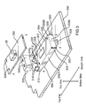
- Fig. 3 is an exploded upper perspective view of a schematic of selected components of the device of Fig. 1, including a printed circuit board (PCB), a speaker, a speaker platform, a RF shield and a speaker connector;
- PCB printed circuit board
- Fig. 4 is an exploded side view of a schematic of selected components of the device of Figs. 1 and 3, including the PCB, speaker, RF shield and speaker connector;
- Fig. 5 is upper perspective view of a schematic of the RF shield of Fig. 3;
- Fig. 6 is top view of a schematic of the RF shield of Fig. 3;
- Fig. 7 is a side view of a schematic of the RF shield of Fig. 6 along the lines A-A;
- Fig. 8 is top view of a schematic of the speaker platform of Fig. 3.
- Fig. 9 is a side view of a schematic of the speaker connector of Fig. 3.
- Fig. 1 illustrates a handheld mobile communication device 10 and its components, including a housing 12, an input device (e.g. keyboard 14A and / or thumbwheel 14B) and an output device (a display 16), which is preferably a graphic liquid crystal display (LCD), although other types of output devices may alternatively be utilized.
- housing 12 is a moulded polycarbonate structure and may be formed via known plastic injection moulding techniques.
- housing 12 typically comprises two or more pieces which fit together in a fitted arrangement to enclose the internal devices and form an exterior casing for device 10.
- housing 12 may comprise an upper housing 12A and a lower housing 12B.
- housing 12 may be elongated vertically, or may take on other sizes and shapes (including clamshell housing structures).
- Speaker 28 and microphone 30 are located within housing 12 and provide audible input and output components for device 10. Openings within housing 12A around each of speaker 28 and microphone 30 allow audible signals to pass between the interior of device 10 and the exterior of device 10.
- PCB 200 comprises a series of internal conductive tracks that form circuits for the components of device 10. Briefly, a description of selected components of device 10 follows.
- a processing device (a microprocessor 18) is shown as coupled between keyboard 14A, display 16 and a series of other internal devices to device 10.
- the microprocessor 18 controls the operation of the display 16, as well as the overall operation of device 10, in response to actuation of keys on the keyboard 14A or thumbwheel 14B by a user.
- Exemplary microprocessors for microprocessor 18 include Data 950 (trade-mark) series microprocessors and the 6200 series microprocessor, both available from Intel Corporation.
- a communication subsystem 20 In addition to microprocessor 18, other internal components of device 10 are include: a communication subsystem 20, a short-range communication subsystem 22, a set of auxiliary I/O devices 24, a serial port 26, speaker 28 and microphone 30.
- Memory for device 10 is provided in flash memory 32 and random access memory (RAM) 34.
- RAM random access memory
- Internal devices are enclosed within housing 12 and typically are either mounted onto a printed circuit board (PCB), affixed to an interior part of the housing or suspended by some means within housing 12.
- PCB printed circuit board
- Device 10 is preferably a two-way radio frequency (RF) communication device having voice and data communication capabilities.
- device 10 preferably has the capability to communicate with other computer systems via the Internet.
- RF radio frequency
- Operating system software executed by the microprocessor 18 is preferably stored in a computer readable medium, such as flash memory 32, but may be stored in other types of memory devices, such as read only memory (ROM) or similar storage element.
- system software, specific device applications, or parts thereof may be temporarily loaded into a volatile store, such as RAM 34.
- Communication signals received by the mobile device may also be stored to RAM 34.
- Microprocessor 18 in addition to its operating system functions, enables execution of software applications on device 10.
- a set of software applications that control basic device operations such as a voice communication module 36A and a data communication module 36B, may be installed on device 10 during manufacture or downloaded thereafter.
- Cell mapping module 36C may also be installed on device 10 during manufacture.
- additional software modules illustrated as an other software module 36N, which may be, for instance, a personal information manager (PIM) application, may be installed during manufacture or downloaded thereafter into device 10.
- PIM application is preferably capable of organizing and managing data items, such as e-mail messages, calendar events, voice mail messages, appointments, and task items.
- PIM application is also preferably capable of sending and receiving data items via a wireless network 38.
- Communication functions including data and voice communications, are performed through communication subsystem 20, and possibly through short-range communication subsystem 22.
- Communication subsystem 20 includes receiver 40, transmitter 42 and one or more antennae, illustrated as receive antenna 44 and transmit antenna 46.
- communication subsystem 20 also includes processing module, such as digital signal processor (DSP) 48 and local oscillators (LOs) 50.
- DSP digital signal processor
- LOs local oscillators
- communication subsystem 20 of device 10 may be designed to operate with the Mobitex (trade-mark), DataTAC (trade-mark) or General Packet Radio Service (GPRS) mobile data communication networks and also designed to operate with any of a variety of voice communication networks, such as Advanced Mobile Phone Service (AMPS), Time Division Multiple Access (TDMA), Code Division Multiple Access (CDMA), Personal Communication Service (PCS), Global System for Mobile Communication (GSM), etc.
- AMPS Advanced Mobile Phone Service
- TDMA Time Division Multiple Access
- CDMA Code Division Multiple Access
- PCS Personal Communication Service
- GSM Global System for Mobile Communication
- Other types of data and voice networks, both separate and integrated may also be utilized with device 10. It will be appreciated that some signals received and transmitted through subsystem 20 may provide interfering signals with other components in device 10, such as microphone 30.
- Network access requirements vary depending upon the type of communication system which can communicate with device 10. For example, in the Mobitex (trade-mark) and DataTAC (trade-mark) networks, mobile devices are registered on the network using a unique Personal Identification Number (PIN) associated with each device. In GPRS networks, however, network access is associated with a subscriber or user of a device. A GPRS device therefore requires a subscriber identity module, commonly referred to as a Subscriber Identity Module (SIM) card, in order to operate on a GPRS network.
- SIM Subscriber Identity Module
- device 10 may send and receive communication signals over communication network 38.
- Signals received from communication network 38 by the receive antenna 44 are routed to receiver 40, which provides for signal amplification, frequency down conversion, filtering, channel selection, etc., and may also provide analog to digital conversion. Analog-to-digital conversion of received signals allows DSP 48 to perform more complex communication functions, such as signal demodulation and decoding.
- signals to be transmitted to network 38 are processed (e.g., modulated and encoded) by DSP 48 and are then provided to transmitter 42 for digital to analog conversion, frequency up conversion, filtering, amplification and transmission to communication network 38 (or networks) via the transmit antenna 46.
- DSP 48 provides for control of receiver 40 and transmitter 42. For example, gains applied to communication signals in receiver 40 and transmitter 42 may be adaptively controlled through automatic gain control algorithms implemented in DSP 48.
- a received signal such as a text message or web page download
- the communication subsystem 20 is input to microprocessor 18.
- the received signal is then further processed by microprocessor 18 for an output to the display 16, or alternatively to some other auxiliary I/O devices 24.
- a user may also compose data items, such as e-mail messages, using keyboard (keypad) 14A, thumbwheel 14B and/or some other auxiliary I/O device 24, such as a touchpad, a rocker switch or some other type of input device.
- the composed data items may then be transmitted over communication network 38 via communication subsystem 20.
- a voice communication mode In a voice communication mode, overall operation of device 10 is substantially similar to the data communication mode, except that received signals are output to speaker 28, and received audio signals are provided to microphone 30 for further conversion into an electrical signal and further processing by device 10.
- Microphone 30 is preferably a silicon-based transducer which can be mounted to PCB 200.
- Speaker 28 as will be described in further detail below, is mounted on speaker platform 202.
- Short-range communication subsystem 22 enables communication between device 10 and other proximate systems or devices, which need not necessarily be similar devices.
- the short-range communication subsystem may include an infrared device and associated circuits and components, or a Bluetooth (trade-mark) communication module to provide for communication with similarly-enabled systems and devices.
- Powering the entire electronics of the mobile handheld communication device is power source 52.
- the power source 52 includes one or more batteries. More preferably, the power source 52 is a single battery pack, especially a rechargeable battery pack.
- Fig. 3 depicts a typical layout of components of device 10.
- references to top side, bottom side, left and right sides, top and bottom ends are provided using the orientation rose of PCB 200 as shown in Fig. 3.
- the top side of the PCB is the front facing side having display 16 mounted thereto.
- the top end of the PCB is the end where the display is mounted.
- a notable feature of an embodiment allows one or more components for device 10 to be mounted on top of one or more components, instead of the typical flat arrangement of components on PCB 200.
- features are provided which facilitate the mounting and aligning of the top component on the bottom component, preferably without using a jig or a tool to align the top component on the bottom one.
- the notable features are provided through speaker platform 202 which is mounted on top of RF shield 300 on PCB 200. Further detail is provided on these features.
- PCB 200 provides a substrate for components of device 10.
- Many components are SMT components and are mounted via a SMT process.
- Other through hole components may be mounted through pick-and-place through hole machines.
- Still other components may be manually placed on PCB 200.
- Some of these components may require RF shielding because they are sensitive to external RF noise.
- Microphone 30 may be such a component.
- Other components may emit RF signals which need to be shielded from other components.
- other shields may be used, e.g. light shields, noise shields, heat shields or any other type of shield known in the art.
- RF shield 300 is provided.
- other shields may be provided.
- shielding properties may be foregone.
- RF shield 300 is a stamped metal piece shaped to define a cap 302.
- Cap 302 has a top 304 and sides 306 to form a body.
- the volume defined under the sides 306 and top 304 define a perimeter of cap 302, with top 304 providing the top of cap 302.
- shield 300 is mounted on PCB 200, shield 300 is preferably fitted and shaped to sit on top of and fully enclose component 308 which has been previously mounted to PCB 200.
- Component 308 may be a surface mount component, a through hole component or a manually mounted component.
- component 308 may benefit from being isolated from other components outside the region where shield 300 is mounted.
- shield 300 When shield 300 is mounted on PCB 200, no significant air gaps are defined underneath top 304 and between sides 306 and PCB 200.
- side 306D has small extensions 328 on its lateral ends which interlock with corresponding extensions 330 on the lateral ends of each side 306A and 306B.
- RF shield provides proper RF shielding to component 308 and other components contained underneath cap 302.
- Three vents 332 are provided on top 304. The vents provide an alignment target for pick-and-place machines for mounting shield 300 on PCB 200.
- RF shield 300 may contact with a ground pad (not shown) on PCB 200.
- the ground pad may have an internal connection to a ground plane in PCB 200. This contact provides a grounding path for shield 300.
- Speaker platform 202 is preferably mounted on top of shield 300.
- Platform 202 provides a substrate for speaker 28 and contains electrical connection tracks therein. It is also preferably a PCB.
- connector 320 which preferably provides a physical connection between connection pads 318 on PCB 200 and connection pads 322 on platform 202. Further detail on platform 202 is provided later.
- RF shield 300 has arms 310 extending outwardly from opposing sides 306A and 306B at the end of side 306C. At the end of each arm 310, a 90° turn inward is provided to produce side arms 312, which are oriented to be generally parallel to side 306C. There is a gap between the ends of arms 312. Along a top edge 314 of each side arm 312 is an upwardly protruding tab 316 located at approximately the mid-way point along each side arm 312. In other embodiments, the side arms 312 can be turned inward at other angles. In other embodiments, the side arms 312 may be connected to each other, forming a part of a loop. The loop is completed by arms 310 and side 306C.
- arms 310 and side arms 312 define a perimeter which rests over a series of connectors 318 on the top surface of PCB 200.
- the perimeter is shaped to cooperate with the body of a connector 320 so that connector 320 fits snugly within the perimeter and is held by a friction fit by the friction interaction of arms 310 and 312 and side 306C and its body.
- shield 300 may have other shapes, sizes, dimensions, features or extensions which operate to align and / or hold connector 320 in place.
- other securing systems may be provided using shapes and features which are separate from shield 300.
- connector 320 has an oblong body 900 which has internal electrical connections 902 therein.
- electrical pads 904 are provided on the bottom surface of body 900.
- electrical pads 906 are provided on the top surface of body 900.
- Internal connections 902 inside body 900 provide electrical continuity between pads 904 and 906.
- pads 904 make contact with pads 318 on PCB 200.
- the height of body 900 is made such that the top end of body 900 extends slightly above the top edge of shield 300.
- Connector 320 is preferably made from a compressible material, and may be implemented as a zebra strip or a polystrip having embedded connectors therein.
- connector 320 compresses slightly and pads 906 on connector 320 make contact with pads 322 on the bottom side of platform 202. Compression of connector 320 aids in providing a sound electrical contact between pads 904 and 906 and their corresponding pads on PCB 200 and platform 202 respectively.
- Connector 320 is typically inserted by hand during the assembly process for device 10. In other embodiments, other components may be placed in the perimeter, per design requirements made for the particular system.
- connector 320 may be used.
- another connector may be a segment of ribbon cable.
- speaker platform 202 is mounted to the top of RF shield 300.
- Apertures 800 in platform 202 are sized and spaced to align with and receive tabs 316.
- platform 202 can quickly mounted to shield 300 by aligning apertures 800 with tabs 316 and then resting platform 202 on top of shield 300.
- a strip of double-sided adhesive tape 324 may be first located on top 304 of shield 300. The location of apertures 800 are arranged such that when tabs 316 are inserted there through, the expected position of connector 320 with its top pads 906 align with pads 322 on the bottom side of platform 202. Assembly and alignment of all components is preferably accomplished without additional jigs or tools needed.
- an alignment system has one feature on either the shield or the platform which positively mates with a corresponding feature on the corresponding platform or shield.
- the features are complementary to each other.
- one feature may be a positive feature, such as protrusion, tab, flange or the like.
- the complementary feature may be a negative feature, such as an aperture, void, opening, notch of the like. It will be further appreciated that the position, size, shape, number and locations of tabs and apertures between shield 300 and platform 202 may be changed, moved and reconfigured as needed.
- another alignment system may utilize a flange interacting with a notch.
- the notch may be located on the shield and the flange on the platform or vice versa. Additionally, the location of flanges and notches may alternate between the shield and the platform. Further, in other embodiments, alignment features may be provided from the PCB 200 or through other one or more other components mounted on PCB 200.
- an electrical connection is present from pads 318 to pads 322.
- the circuit associated with speaker 28 is carried through the two connections represented by pads 318.
- interior tracks within platform 202 provide a connection to between pads 322 on the lower surface of platform 202 to pads 802 on the upper surface of platform 202.
- the location of pads 802 is preferably provided such that they align with the connections on the bottom of speaker 28.
- the location of pads 802 may be offset from being directly over pads 318 on PCB 200.
- platform 202 may also be used to locate speaker 28 in a location which is immediately above another component, such as a component contained within cap 302. Speaker 28 may simply sit on platform 202 in place and an electrical circuit may be completed to pads 318.
- housing 12A may have a shaped area 326 which can receive the top portion of speaker 28 and keep it in place. Some more double-sided adhesive tape may be used to tack speaker 28 to housing 12A. When all relevant components are mounted on PCB 200, housings 12A and 12B may be mated together and speaker 28 is received in shaped area 326.
- shield 300 may be replaced with a different structure that allows components to be located underneath and above it.
- a speaker with a connector being connected to the PCB and a connection system therefor
- other electronic devices not necessarily incorporating a speaker, but having a connection from a PCB to a location above the PCB may be used.
- Such electronic devices may include a populated daughterboard, a microprocessor, memory devices and electro-mechanical devices, such as relays.
Landscapes
- Engineering & Computer Science (AREA)
- Microelectronics & Electronic Packaging (AREA)
- Shielding Devices Or Components To Electric Or Magnetic Fields (AREA)
- Supply And Installment Of Electrical Components (AREA)
- Telephone Set Structure (AREA)
- Connector Housings Or Holding Contact Members (AREA)
- Photoreceptors In Electrophotography (AREA)
Abstract
Description
- The invention described herein relates to method and system for assembling components in a handheld electronic device. In particular, the invention described herein relates to an arrangement for components mounted around a casing, such as an RF shield, mounted on a PCB in the device.
- A handheld electronic device, such as a personal digital assistant (PDA) or wireless telephone, includes a keyboard/keypad, a display, a speaker, a microphone, printed circuit board (PCB) disposed within a common housing. There is a constant push to reduce the size of such a device. In some form factors, it is necessary to stack components on top of each other. As the devices become smaller, manufacturing techniques become more complicated. Surface mount technologies (SMT) incorporate a wide complement of reduced size components. High-speed pick and place assembling machines can populate a PCB with SMT components very efficiently. However, some components are not compatible with SMT placement machines, because their dimensions or their connection requirements are not compatible with such placement machines. Generally, such incompatible devices are mounted manually. For some components, specialized tools or jigs are often required to be mounted on the PCB during the manufacturing process in order to properly align and affix the components to the board. The use of specialized jigs requires additional toolings to be made. Also, assembling of these devices is slowed because the jig must be aligned with the PCB, then the component must be aligned with the jig and mounted to the PCB and finally, the jig must be removed from the PCB.
- There is a need to address deficiencies in the prior art.
- In a first aspect of an embodiment, a system of components in an electronic device is provided. The system preferably comprises: a PCB; a first component mounted to the PCB; a cap located about the first component; a second component; and a platform for the second component. In the system, the platform and the cap cooperate via alignment features such that the platform may be placed on top of the cap at a predetermined location utilizing the alignment features.
- The system may further comprise a connector disposed between the platform and the PCB. The connector may provide electrical connections between the PCB and the platform for the second component.
- In the system, the platform may provide connections to offset the second component from a location of corresponding pads on the PCB.
- In the system, the cap may comprise at least one arm to position the connector in place. The arm may comprise an upwardly extending tab. The arm may extend outwardly from the body of the cap. The platform may comprise an aperture to receive the tab. The tab may be received in the aperture when the platform is mounted about the cap.
- In the system, the arm may have a first side arm extending at an angle from its end; and the second arm may have a second side arm extending at an angle from its end. Also, the side arms may extend towards each other and cooperate with the body to retain the connector in place.
- In the system the cap may comprise a second arm to position the connector in place. The second arm may comprise a second upwardly extending tab. The platform may comprise a second aperture to receive the second tab. The second tab may be received in the second aperture when said platform is mounted about the cap.
- In the system, the electronic device may be a portable communication device; the second component may be a speaker; and the cap may provide RF shielding for the first component.
- In a second aspect, a method of assembling components in an electronic device is provided. The device comprises a PCB, a first component mounted to the PCB, a cap located about the first component, a second component and a platform for the second component. The method comprises: assembling the platform onto the cap without utilizing an external jig and utilizing alignment features provided on the cap and the platform, such that the platform may be placed on top of the cap at a predetermined location about the cap defined by the alignment features.
- In the method, the cap may comprise an arm to position the connector in place.
The arm may comprise an upwardly extending tab. The platform may comprise an aperture to receive the tab. Also, the tab may be received in the aperture when the platform is mounted about the cap. - In the method, the cap may comprise a second arm to position the connector in place. The second arm may comprise a second upwardly extending tab. The platform may comprise a second aperture to receive the second tab. The second tab may be received in the second aperture when said platform is mounted about the cap.
- In the method, the electronic device may be a portable communication device; the second component may be a speaker; and the cap may provide RF shielding for the first component.
- In other aspects various combinations of sets and subsets of the above aspects are provided.
- The invention will now be described by way of example only with reference to the accompanying drawings in which:
- Fig. 1 is a front plan view of schematic of a handheld electronic device assembled through an embodiment of the invention described herein;
- Fig. 2 is a block diagram of the components of the electronic device of Fig. 1, including a speaker assembly relating to an embodiment;
- Fig. 3 is an exploded upper perspective view of a schematic of selected components of the device of Fig. 1, including a printed circuit board (PCB), a speaker, a speaker platform, a RF shield and a speaker connector;
- Fig. 4 is an exploded side view of a schematic of selected components of the device of Figs. 1 and 3, including the PCB, speaker, RF shield and speaker connector;
- Fig. 5 is upper perspective view of a schematic of the RF shield of Fig. 3;
- Fig. 6 is top view of a schematic of the RF shield of Fig. 3;
- Fig. 7 is a side view of a schematic of the RF shield of Fig. 6 along the lines A-A;
- Fig. 8 is top view of a schematic of the speaker platform of Fig. 3; and
- Fig. 9 is a side view of a schematic of the speaker connector of Fig. 3.
- The description which follows and the embodiments described therein are provided by way of illustration of an example or examples of particular embodiments of the principles of the present invention. These examples are provided for the purposes of explanation, and not limitation, of those principles and of the invention. In the description which follows, like parts are marked throughout the specification and the drawings with the same respective reference numerals.
- Fig. 1 illustrates a handheld
mobile communication device 10 and its components, including ahousing 12, an input device (e.g. keyboard 14A and / orthumbwheel 14B) and an output device (a display 16), which is preferably a graphic liquid crystal display (LCD), although other types of output devices may alternatively be utilized. Typically,housing 12 is a moulded polycarbonate structure and may be formed via known plastic injection moulding techniques. To assist in assembly ofdevice 10,housing 12 typically comprises two or more pieces which fit together in a fitted arrangement to enclose the internal devices and form an exterior casing fordevice 10. For example,housing 12 may comprise anupper housing 12A and alower housing 12B. Physically fordevice 10,housing 12 may be elongated vertically, or may take on other sizes and shapes (including clamshell housing structures).Speaker 28 andmicrophone 30 are located withinhousing 12 and provide audible input and output components fordevice 10. Openings withinhousing 12A around each ofspeaker 28 andmicrophone 30 allow audible signals to pass between the interior ofdevice 10 and the exterior ofdevice 10. - Referring to Fig. 2, components for
device 10 are shown. Generally, all components are connected to or mounted onPCB 200.PCB 200 comprises a series of internal conductive tracks that form circuits for the components ofdevice 10. Briefly, a description of selected components ofdevice 10 follows. - First, a processing device (a microprocessor 18) is shown as coupled between
keyboard 14A,display 16 and a series of other internal devices todevice 10. Themicroprocessor 18 controls the operation of thedisplay 16, as well as the overall operation ofdevice 10, in response to actuation of keys on thekeyboard 14A orthumbwheel 14B by a user. Exemplary microprocessors formicroprocessor 18 include Data 950 (trade-mark) series microprocessors and the 6200 series microprocessor, both available from Intel Corporation. - In addition to
microprocessor 18, other internal components ofdevice 10 are include: acommunication subsystem 20, a short-range communication subsystem 22, a set of auxiliary I/O devices 24, aserial port 26,speaker 28 andmicrophone 30. Memory fordevice 10 is provided inflash memory 32 and random access memory (RAM) 34. Internal devices are enclosed withinhousing 12 and typically are either mounted onto a printed circuit board (PCB), affixed to an interior part of the housing or suspended by some means withinhousing 12. -
Device 10 is preferably a two-way radio frequency (RF) communication device having voice and data communication capabilities. In addition,device 10 preferably has the capability to communicate with other computer systems via the Internet. - Operating system software executed by the
microprocessor 18 is preferably stored in a computer readable medium, such asflash memory 32, but may be stored in other types of memory devices, such as read only memory (ROM) or similar storage element. In addition, system software, specific device applications, or parts thereof, may be temporarily loaded into a volatile store, such asRAM 34. Communication signals received by the mobile device may also be stored toRAM 34. -
Microprocessor 18, in addition to its operating system functions, enables execution of software applications ondevice 10. A set of software applications that control basic device operations, such as avoice communication module 36A and adata communication module 36B, may be installed ondevice 10 during manufacture or downloaded thereafter.Cell mapping module 36C may also be installed ondevice 10 during manufacture. As well, additional software modules, illustrated as another software module 36N, which may be, for instance, a personal information manager (PIM) application, may be installed during manufacture or downloaded thereafter intodevice 10. PIM application is preferably capable of organizing and managing data items, such as e-mail messages, calendar events, voice mail messages, appointments, and task items. PIM application is also preferably capable of sending and receiving data items via a wireless network 38. - Communication functions, including data and voice communications, are performed through
communication subsystem 20, and possibly through short-range communication subsystem 22.Communication subsystem 20 includesreceiver 40,transmitter 42 and one or more antennae, illustrated as receive antenna 44 and transmitantenna 46. In addition,communication subsystem 20 also includes processing module, such as digital signal processor (DSP) 48 and local oscillators (LOs) 50. The specific design and implementation ofcommunication subsystem 20 is dependent upon the communication network in whichdevice 10 is intended to operate. For example,communication subsystem 20 ofdevice 10 may be designed to operate with the Mobitex (trade-mark), DataTAC (trade-mark) or General Packet Radio Service (GPRS) mobile data communication networks and also designed to operate with any of a variety of voice communication networks, such as Advanced Mobile Phone Service (AMPS), Time Division Multiple Access (TDMA), Code Division Multiple Access (CDMA), Personal Communication Service (PCS), Global System for Mobile Communication (GSM), etc. Other types of data and voice networks, both separate and integrated, may also be utilized withdevice 10. It will be appreciated that some signals received and transmitted throughsubsystem 20 may provide interfering signals with other components indevice 10, such asmicrophone 30. - Network access requirements vary depending upon the type of communication system which can communicate with
device 10. For example, in the Mobitex (trade-mark) and DataTAC (trade-mark) networks, mobile devices are registered on the network using a unique Personal Identification Number (PIN) associated with each device. In GPRS networks, however, network access is associated with a subscriber or user of a device. A GPRS device therefore requires a subscriber identity module, commonly referred to as a Subscriber Identity Module (SIM) card, in order to operate on a GPRS network. - When required network registration or activation procedures have been completed,
device 10 may send and receive communication signals over communication network 38. Signals received from communication network 38 by the receive antenna 44 are routed toreceiver 40, which provides for signal amplification, frequency down conversion, filtering, channel selection, etc., and may also provide analog to digital conversion. Analog-to-digital conversion of received signals allowsDSP 48 to perform more complex communication functions, such as signal demodulation and decoding. In a similar manner, signals to be transmitted to network 38 are processed (e.g., modulated and encoded) byDSP 48 and are then provided totransmitter 42 for digital to analog conversion, frequency up conversion, filtering, amplification and transmission to communication network 38 (or networks) via the transmitantenna 46. - In addition to processing communication signals,
DSP 48 provides for control ofreceiver 40 andtransmitter 42. For example, gains applied to communication signals inreceiver 40 andtransmitter 42 may be adaptively controlled through automatic gain control algorithms implemented inDSP 48. - In a data communication mode, a received signal, such as a text message or web page download, is processed by the
communication subsystem 20 and is input tomicroprocessor 18. The received signal is then further processed bymicroprocessor 18 for an output to thedisplay 16, or alternatively to some other auxiliary I/O devices 24. A user may also compose data items, such as e-mail messages, using keyboard (keypad) 14A,thumbwheel 14B and/or some other auxiliary I/O device 24, such as a touchpad, a rocker switch or some other type of input device. The composed data items may then be transmitted over communication network 38 viacommunication subsystem 20. - In a voice communication mode, overall operation of
device 10 is substantially similar to the data communication mode, except that received signals are output tospeaker 28, and received audio signals are provided tomicrophone 30 for further conversion into an electrical signal and further processing bydevice 10.Microphone 30 is preferably a silicon-based transducer which can be mounted toPCB 200.Speaker 28, as will be described in further detail below, is mounted onspeaker platform 202. - Short-
range communication subsystem 22 enables communication betweendevice 10 and other proximate systems or devices, which need not necessarily be similar devices. For example, the short-range communication subsystem may include an infrared device and associated circuits and components, or a Bluetooth (trade-mark) communication module to provide for communication with similarly-enabled systems and devices. - Powering the entire electronics of the mobile handheld communication device is
power source 52. Preferably, thepower source 52 includes one or more batteries. More preferably, thepower source 52 is a single battery pack, especially a rechargeable battery pack. - Fig. 3 depicts a typical layout of components of
device 10. For the purposes of illustration, references to top side, bottom side, left and right sides, top and bottom ends are provided using the orientation rose ofPCB 200 as shown in Fig. 3. Therein, the top side of the PCB is the front facingside having display 16 mounted thereto. The top end of the PCB is the end where the display is mounted. These references provide relative positional references for components for convenience only and are not meant to be limiting, unless otherwise noted. - A notable feature of an embodiment allows one or more components for
device 10 to be mounted on top of one or more components, instead of the typical flat arrangement of components onPCB 200. As a further feature, when one component is mounted on top of another component, features are provided which facilitate the mounting and aligning of the top component on the bottom component, preferably without using a jig or a tool to align the top component on the bottom one. In one embodiment, the notable features are provided throughspeaker platform 202 which is mounted on top ofRF shield 300 onPCB 200. Further detail is provided on these features. - As noted before,
PCB 200 provides a substrate for components ofdevice 10.
Many components are SMT components and are mounted via a SMT process. Other through hole components may be mounted through pick-and-place through hole machines. Still other components may be manually placed onPCB 200. Some of these components may require RF shielding because they are sensitive to external RF noise.Microphone 30 may be such a component. Other components may emit RF signals which need to be shielded from other components. In other aspects, other shields may be used, e.g. light shields, noise shields, heat shields or any other type of shield known in the art. To assist with a RF shielding,RF shield 300 is provided. In other embodiments, other shields may be provided. Further in other embodiments, shielding properties may be foregone. -
RF shield 300 is a stamped metal piece shaped to define acap 302.Cap 302 has a top 304 andsides 306 to form a body. The volume defined under thesides 306 and top 304 define a perimeter ofcap 302, with top 304 providing the top ofcap 302. In the embodiment, there are foursides 306 forcap 302. When aspecific side 302 is being referenced, it is noted with a suffix A, B, C or D as appropriate. Whenshield 300 is mounted onPCB 200,shield 300 is preferably fitted and shaped to sit on top of and fully enclosecomponent 308 which has been previously mounted toPCB 200.Component 308 may be a surface mount component, a through hole component or a manually mounted component. For performance or sensitivity reasons,component 308 may benefit from being isolated from other components outside the region whereshield 300 is mounted. Whenshield 300 is mounted onPCB 200, no significant air gaps are defined underneathtop 304 and betweensides 306 andPCB 200. In one embodiment,side 306D hassmall extensions 328 on its lateral ends which interlock withcorresponding extensions 330 on the lateral ends of eachside component 308 and other components contained underneathcap 302. Threevents 332 are provided ontop 304. The vents provide an alignment target for pick-and-place machines for mountingshield 300 onPCB 200. -
RF shield 300 may contact with a ground pad (not shown) onPCB 200. The ground pad may have an internal connection to a ground plane inPCB 200. This contact provides a grounding path forshield 300. -
Speaker platform 202 is preferably mounted on top ofshield 300.Platform 202 provides a substrate forspeaker 28 and contains electrical connection tracks therein. It is also preferably a PCB. In order to provide electrical contacts betweenPCB 200 andplatform 202,connector 320 which preferably provides a physical connection betweenconnection pads 318 onPCB 200 andconnection pads 322 onplatform 202. Further detail onplatform 202 is provided later. - In order to provide a securing system for
connector 320, preferablyRF shield 300 hasarms 310 extending outwardly from opposingsides side 306C. At the end of eacharm 310, a 90° turn inward is provided to produceside arms 312, which are oriented to be generally parallel toside 306C. There is a gap between the ends ofarms 312. Along atop edge 314 of eachside arm 312 is an upwardlyprotruding tab 316 located at approximately the mid-way point along eachside arm 312. In other embodiments, theside arms 312 can be turned inward at other angles. In other embodiments, theside arms 312 may be connected to each other, forming a part of a loop. The loop is completed byarms 310 andside 306C. -
Side 306C,arms 310 andside arms 312 define a perimeter which rests over a series ofconnectors 318 on the top surface ofPCB 200. The perimeter is shaped to cooperate with the body of aconnector 320 so thatconnector 320 fits snugly within the perimeter and is held by a friction fit by the friction interaction ofarms side 306C and its body. - In still other embodiments, shield 300 may have other shapes, sizes, dimensions, features or extensions which operate to align and / or hold
connector 320 in place. In still other embodiments, other securing systems may be provided using shapes and features which are separate fromshield 300. - Referring to Figs. 3, 4 and 9,
connector 320 has anoblong body 900 which has internalelectrical connections 902 therein. On the bottom surface ofbody 900,electrical pads 904 are provided. On the top surface ofbody 900electrical pads 906 are provided.Internal connections 902 insidebody 900 provide electrical continuity betweenpads body 900 is fitted snugly into the perimeter defined byarms side 306C,pads 904 make contact withpads 318 onPCB 200. Preferably, the height ofbody 900 is made such that the top end ofbody 900 extends slightly above the top edge ofshield 300.Connector 320 is preferably made from a compressible material, and may be implemented as a zebra strip or a polystrip having embedded connectors therein. Whenspeaker platform 202 is subsequently mounted in place on top ofshield 300,connector 320 compresses slightly andpads 906 onconnector 320 make contact withpads 322 on the bottom side ofplatform 202. Compression ofconnector 320 aids in providing a sound electrical contact betweenpads PCB 200 andplatform 202 respectively. -
Connector 320 is typically inserted by hand during the assembly process fordevice 10. In other embodiments, other components may be placed in the perimeter, per design requirements made for the particular system. - In other embodiments, other shapes and forms for
connector 320 may be used. For example, another connector may be a segment of ribbon cable. - Referring to Figs. 3, 4 and 8, after
connector 320 is inserted in place aboutshield 300,speaker platform 202 is mounted to the top ofRF shield 300.Apertures 800 inplatform 202 are sized and spaced to align with and receivetabs 316. As such in anassembly process platform 202 can quickly mounted to shield 300 by aligningapertures 800 withtabs 316 and then restingplatform 202 on top ofshield 300. To fixplatform 202 to shield 300, a strip of double-sidedadhesive tape 324 may be first located ontop 304 ofshield 300. The location ofapertures 800 are arranged such that whentabs 316 are inserted there through, the expected position ofconnector 320 with itstop pads 906 align withpads 322 on the bottom side ofplatform 202. Assembly and alignment of all components is preferably accomplished without additional jigs or tools needed. - It will be appreciated that the interaction between
tabs 316 onshield 300 andapertures 800 onplatform 202 provide an alignment system for mountingplatform 202 aboutshield 300. In other embodiments, other alignment systems can be provided. Generally, an alignment system has one feature on either the shield or the platform which positively mates with a corresponding feature on the corresponding platform or shield. The features are complementary to each other. For example one feature may be a positive feature, such as protrusion, tab, flange or the like. The complementary feature may be a negative feature, such as an aperture, void, opening, notch of the like. It will be further appreciated that the position, size, shape, number and locations of tabs and apertures betweenshield 300 andplatform 202 may be changed, moved and reconfigured as needed. For example, another alignment system may utilize a flange interacting with a notch. The notch may be located on the shield and the flange on the platform or vice versa. Additionally, the location of flanges and notches may alternate between the shield and the platform. Further, in other embodiments, alignment features may be provided from thePCB 200 or through other one or more other components mounted onPCB 200. - As such, an electrical connection is present from
pads 318 topads 322. For the embodiment, the circuit associated withspeaker 28 is carried through the two connections represented bypads 318. In order to complete the circuit, interior tracks withinplatform 202 provide a connection to betweenpads 322 on the lower surface ofplatform 202 topads 802 on the upper surface ofplatform 202. The location ofpads 802 is preferably provided such that they align with the connections on the bottom ofspeaker 28. Also the location ofpads 802 may be offset from being directly overpads 318 onPCB 200. As such,platform 202 may also be used to locatespeaker 28 in a location which is immediately above another component, such as a component contained withincap 302.Speaker 28 may simply sit onplatform 202 in place and an electrical circuit may be completed topads 318. Some double-sided adhesive tape may be used to tackspeaker 28 toplatform 202.Housing 12A may have a shapedarea 326 which can receive the top portion ofspeaker 28 and keep it in place. Some more double-sided adhesive tape may be used to tackspeaker 28 tohousing 12A. When all relevant components are mounted onPCB 200,housings speaker 28 is received in shapedarea 326. - It will be appreciated in other embodiments that other components may be mounted on top of
shield 300. Alternatively, no components may need to be mounted onplatform 202 on top ofshield 300. Further still, in other embodiments, shield 300 may be replaced with a different structure that allows components to be located underneath and above it. - Further still, although the embodiments have been described in terms of a speaker with a connector being connected to the PCB and a connection system therefor, in other embodiments, other electronic devices, not necessarily incorporating a speaker, but having a connection from a PCB to a location above the PCB may be used. Such electronic devices may include a populated daughterboard, a microprocessor, memory devices and electro-mechanical devices, such as relays.
- The present invention is defined by the claims appended hereto, with the foregoing description being merely illustrative of a preferred embodiment of the invention. Those of ordinary skill may envisage certain modifications to the foregoing embodiments which, although not explicitly discussed herein, do not depart from the scope of the invention, as defined by the appended claims.
Claims (12)
- A system of components in an electronic device, comprising:a PCB;a first component mounted to said PCB;a cap located about said first component;a second component; anda platform for said second component,wherein said platform and said cap cooperate via alignment features on each of said platform and said cap such that said platform may be placed on top of said cap at a predetermined location utilizing said alignment features.
- The system as claimed in claim 1, further comprising:a connector disposed between said platform and said PCB, said connector providing electrical connections between said PCB and said platform for said second component.
- The system as claimed in claim 2, wherein
said platform provides connections to offset said second component from a location of pads on said PCB. - The system as claimed in claim 3, wherein
said cap comprises an arm to position said connector in place, said arm extending outwardly from a body of said cap;
said arm comprises an upwardly extending tab to provide one feature of said alignment features;
said platform comprises an aperture to receive said tab to provide another feature of said alignment features; and
said tab is received in said aperture when said platform is mounted about said cap. - The system as claimed in claim 4, wherein
said cap comprises a second arm to position said connector in place, said second arm extending outwardly from said body of said cap;
said second arm comprises a second upwardly extending tab;
said platform comprises a second aperture to receive said second tab; and
said second tab is received in said second aperture when said platform is mounted about said cap,
wherein said connector is locatable between said first and said second arm to be held therebetween with a friction fit. - The system as claimed in claim 5, wherein
said arm has a first side arm extending at an angle at an end of said arm; and
said second arm has a second side arm extending at an angle at an end of said second arm,
wherein said first and second side arms extend towards each other and cooperate with said body to retain said connector in place. - The system of components as claimed in claim 6, wherein said first and second side arms are connected to each other, forming a part of a loop.
- The system as claimed in claim 7, wherein
said electronic device is a portable communication device;
said second component is a speaker; and
said cap provides RF shielding for said first component. - A method of assembling components in an electronic device comprising a PCB, a first component mounted to said PCB, a cap located about said first component, a second component and a platform for said second component, said method comprising:assembling said platform onto said cap without utilizing an external jig andutilizing alignment features provided on said cap and said platforms, such that said platform may be placed on top of said cap at a predetermined location about said cap defined by said alignment features.
- The method as claimed in claim 9, wherein:said connector is positioned in place by an arm of said cap, said arm comprising an upwardly extending tab; andreceiving said tab in an aperture of said platform;wherein said tab is received in said aperture when said platform is mounted about said cap.
- The method as claimed in claim 10, wherein
said cap comprises a second arm;
said second arm comprises a second upwardly extending tab; and
said platform comprises a second aperture to receive said second tab;
the method comprising receiving said second tab in said second aperture when said platform is mounted about said cap. - The method as claimed in claim 11, wherein:said electronic device is a portable communication device; andsaid second component is a speaker;the method comprising using said cap to provide RF shielding for said first component.
Priority Applications (4)
| Application Number | Priority Date | Filing Date | Title |
|---|---|---|---|
| DE602006001292T DE602006001292D1 (en) | 2006-03-08 | 2006-03-08 | System and method for mounting components in an electronic device |
| AT06110874T ATE396606T1 (en) | 2006-03-08 | 2006-03-08 | SYSTEM AND METHOD FOR MOUNTING COMPONENTS IN AN ELECTRONIC DEVICE |
| EP06110874A EP1833284B1 (en) | 2006-03-08 | 2006-03-08 | System and Method for Assembling Components in an Electronic Device |
| CA2580031A CA2580031C (en) | 2006-03-08 | 2007-03-01 | System and method for assembling components in an electronic device |
Applications Claiming Priority (1)
| Application Number | Priority Date | Filing Date | Title |
|---|---|---|---|
| EP06110874A EP1833284B1 (en) | 2006-03-08 | 2006-03-08 | System and Method for Assembling Components in an Electronic Device |
Publications (2)
| Publication Number | Publication Date |
|---|---|
| EP1833284A1 true EP1833284A1 (en) | 2007-09-12 |
| EP1833284B1 EP1833284B1 (en) | 2008-05-21 |
Family
ID=36501867
Family Applications (1)
| Application Number | Title | Priority Date | Filing Date |
|---|---|---|---|
| EP06110874A Expired - Lifetime EP1833284B1 (en) | 2006-03-08 | 2006-03-08 | System and Method for Assembling Components in an Electronic Device |
Country Status (4)
| Country | Link |
|---|---|
| EP (1) | EP1833284B1 (en) |
| AT (1) | ATE396606T1 (en) |
| CA (1) | CA2580031C (en) |
| DE (1) | DE602006001292D1 (en) |
Cited By (3)
| Publication number | Priority date | Publication date | Assignee | Title |
|---|---|---|---|---|
| EP2416544A1 (en) * | 2010-08-06 | 2012-02-08 | Research In Motion Limited | Electromagnetic Shielding and an Acoustic Chamber for a Microphone in a Mobile Electronic Device |
| US8340735B2 (en) | 2010-08-06 | 2012-12-25 | Research In Motion Limited | Electromagnetic shielding and an acoustic chamber for a microphone in a mobile electronic device |
| WO2013095628A1 (en) * | 2011-12-23 | 2013-06-27 | Intel Corpporation | High bandwidth connector for internal and external io interfaces |
Citations (3)
| Publication number | Priority date | Publication date | Assignee | Title |
|---|---|---|---|---|
| JP2003249789A (en) * | 2002-02-22 | 2003-09-05 | Ngk Spark Plug Co Ltd | Electronic components with shield cap |
| JP2004022711A (en) * | 2002-06-14 | 2004-01-22 | Ngk Spark Plug Co Ltd | Electronic components with shield caps |
| EP1513379A2 (en) * | 2003-09-05 | 2005-03-09 | Nec Corporation | Compact radio equipment and method of mounting the same |
-
2006
- 2006-03-08 DE DE602006001292T patent/DE602006001292D1/en not_active Expired - Lifetime
- 2006-03-08 AT AT06110874T patent/ATE396606T1/en not_active IP Right Cessation
- 2006-03-08 EP EP06110874A patent/EP1833284B1/en not_active Expired - Lifetime
-
2007
- 2007-03-01 CA CA2580031A patent/CA2580031C/en not_active Expired - Fee Related
Patent Citations (3)
| Publication number | Priority date | Publication date | Assignee | Title |
|---|---|---|---|---|
| JP2003249789A (en) * | 2002-02-22 | 2003-09-05 | Ngk Spark Plug Co Ltd | Electronic components with shield cap |
| JP2004022711A (en) * | 2002-06-14 | 2004-01-22 | Ngk Spark Plug Co Ltd | Electronic components with shield caps |
| EP1513379A2 (en) * | 2003-09-05 | 2005-03-09 | Nec Corporation | Compact radio equipment and method of mounting the same |
Non-Patent Citations (1)
| Title |
|---|
| PATENT ABSTRACTS OF JAPAN vol. 2003, no. 12 5 December 2003 (2003-12-05) * |
Cited By (5)
| Publication number | Priority date | Publication date | Assignee | Title |
|---|---|---|---|---|
| EP2416544A1 (en) * | 2010-08-06 | 2012-02-08 | Research In Motion Limited | Electromagnetic Shielding and an Acoustic Chamber for a Microphone in a Mobile Electronic Device |
| US8340735B2 (en) | 2010-08-06 | 2012-12-25 | Research In Motion Limited | Electromagnetic shielding and an acoustic chamber for a microphone in a mobile electronic device |
| US8918150B2 (en) | 2010-08-06 | 2014-12-23 | Blackberry Limited | Electromagnetic shielding and an acoustic chamber for a microphone in a mobile electronic device |
| WO2013095628A1 (en) * | 2011-12-23 | 2013-06-27 | Intel Corpporation | High bandwidth connector for internal and external io interfaces |
| US9391378B2 (en) | 2011-12-23 | 2016-07-12 | Intel Corporation | High bandwidth connector for internal and external IO interfaces |
Also Published As
| Publication number | Publication date |
|---|---|
| CA2580031C (en) | 2011-05-03 |
| EP1833284B1 (en) | 2008-05-21 |
| DE602006001292D1 (en) | 2008-07-03 |
| CA2580031A1 (en) | 2007-09-08 |
| ATE396606T1 (en) | 2008-06-15 |
Similar Documents
| Publication | Publication Date | Title |
|---|---|---|
| US7797025B2 (en) | Microphone coupler for a communication device | |
| US9052870B2 (en) | System and frame for mounting a device above a printed circuit board in an electronic device | |
| US8548185B2 (en) | Microphone coupler for a communication device | |
| US7796398B2 (en) | System of components in an electronic device | |
| AU2006202755B2 (en) | Microphone coupler for communication device | |
| CA2580031C (en) | System and method for assembling components in an electronic device | |
| CA2525357C (en) | Microphone coupler for a communication device | |
| EP1691593B1 (en) | Frame for a device mounted above a printed circuit board in an electronic device | |
| US20060279939A1 (en) | Electrical connector and system for a component in an electronic device | |
| EP1780989B1 (en) | Microphone coupler for a communication device | |
| EP1734615B1 (en) | Electrical connector and system for a component in an electronic device | |
| HK1094129B (en) | Frame for a device mounted above a printed circuit board in an electronic device |
Legal Events
| Date | Code | Title | Description |
|---|---|---|---|
| PUAI | Public reference made under article 153(3) epc to a published international application that has entered the european phase |
Free format text: ORIGINAL CODE: 0009012 |
|
| 17P | Request for examination filed |
Effective date: 20060308 |
|
| AK | Designated contracting states |
Kind code of ref document: A1 Designated state(s): AT BE BG CH CY CZ DE DK EE ES FI FR GB GR HU IE IS IT LI LT LU LV MC NL PL PT RO SE SI SK TR |
|
| AX | Request for extension of the european patent |
Extension state: AL BA HR MK YU |
|
| GRAP | Despatch of communication of intention to grant a patent |
Free format text: ORIGINAL CODE: EPIDOSNIGR1 |
|
| RIN1 | Information on inventor provided before grant (corrected) |
Inventor name: KYOWSKI, TIM Inventor name: HAMILTON, JASON EVERETTE |
|
| RIN1 | Information on inventor provided before grant (corrected) |
Inventor name: HAMILTON, JASON EVERETTE Inventor name: KYOWSKI, TIM |
|
| GRAS | Grant fee paid |
Free format text: ORIGINAL CODE: EPIDOSNIGR3 |
|
| GRAA | (expected) grant |
Free format text: ORIGINAL CODE: 0009210 |
|
| AK | Designated contracting states |
Kind code of ref document: B1 Designated state(s): AT BE BG CH CY CZ DE DK EE ES FI FR GB GR HU IE IS IT LI LT LU LV MC NL PL PT RO SE SI SK TR |
|
| AX | Request for extension of the european patent |
Extension state: AL BA HR MK YU |
|
| REG | Reference to a national code |
Ref country code: GB Ref legal event code: FG4D |
|
| REG | Reference to a national code |
Ref country code: CH Ref legal event code: EP |
|
| REF | Corresponds to: |
Ref document number: 602006001292 Country of ref document: DE Date of ref document: 20080703 Kind code of ref document: P |
|
| REG | Reference to a national code |
Ref country code: IE Ref legal event code: FG4D |
|
| PG25 | Lapsed in a contracting state [announced via postgrant information from national office to epo] |
Ref country code: SI Free format text: LAPSE BECAUSE OF FAILURE TO SUBMIT A TRANSLATION OF THE DESCRIPTION OR TO PAY THE FEE WITHIN THE PRESCRIBED TIME-LIMIT Effective date: 20080521 |
|
| PG25 | Lapsed in a contracting state [announced via postgrant information from national office to epo] |
Ref country code: FI Free format text: LAPSE BECAUSE OF FAILURE TO SUBMIT A TRANSLATION OF THE DESCRIPTION OR TO PAY THE FEE WITHIN THE PRESCRIBED TIME-LIMIT Effective date: 20080521 Ref country code: ES Free format text: LAPSE BECAUSE OF FAILURE TO SUBMIT A TRANSLATION OF THE DESCRIPTION OR TO PAY THE FEE WITHIN THE PRESCRIBED TIME-LIMIT Effective date: 20080901 |
|
| NLV1 | Nl: lapsed or annulled due to failure to fulfill the requirements of art. 29p and 29m of the patents act | ||
| PG25 | Lapsed in a contracting state [announced via postgrant information from national office to epo] |
Ref country code: AT Free format text: LAPSE BECAUSE OF FAILURE TO SUBMIT A TRANSLATION OF THE DESCRIPTION OR TO PAY THE FEE WITHIN THE PRESCRIBED TIME-LIMIT Effective date: 20080521 Ref country code: NL Free format text: LAPSE BECAUSE OF FAILURE TO SUBMIT A TRANSLATION OF THE DESCRIPTION OR TO PAY THE FEE WITHIN THE PRESCRIBED TIME-LIMIT Effective date: 20080521 Ref country code: LV Free format text: LAPSE BECAUSE OF FAILURE TO SUBMIT A TRANSLATION OF THE DESCRIPTION OR TO PAY THE FEE WITHIN THE PRESCRIBED TIME-LIMIT Effective date: 20080521 Ref country code: PL Free format text: LAPSE BECAUSE OF FAILURE TO SUBMIT A TRANSLATION OF THE DESCRIPTION OR TO PAY THE FEE WITHIN THE PRESCRIBED TIME-LIMIT Effective date: 20080521 |
|
| PG25 | Lapsed in a contracting state [announced via postgrant information from national office to epo] |
Ref country code: IS Free format text: LAPSE BECAUSE OF FAILURE TO SUBMIT A TRANSLATION OF THE DESCRIPTION OR TO PAY THE FEE WITHIN THE PRESCRIBED TIME-LIMIT Effective date: 20080921 |
|
| PG25 | Lapsed in a contracting state [announced via postgrant information from national office to epo] |
Ref country code: LT Free format text: LAPSE BECAUSE OF FAILURE TO SUBMIT A TRANSLATION OF THE DESCRIPTION OR TO PAY THE FEE WITHIN THE PRESCRIBED TIME-LIMIT Effective date: 20080521 Ref country code: DK Free format text: LAPSE BECAUSE OF FAILURE TO SUBMIT A TRANSLATION OF THE DESCRIPTION OR TO PAY THE FEE WITHIN THE PRESCRIBED TIME-LIMIT Effective date: 20080521 Ref country code: CZ Free format text: LAPSE BECAUSE OF FAILURE TO SUBMIT A TRANSLATION OF THE DESCRIPTION OR TO PAY THE FEE WITHIN THE PRESCRIBED TIME-LIMIT Effective date: 20080521 Ref country code: SE Free format text: LAPSE BECAUSE OF FAILURE TO SUBMIT A TRANSLATION OF THE DESCRIPTION OR TO PAY THE FEE WITHIN THE PRESCRIBED TIME-LIMIT Effective date: 20080821 |
|
| PG25 | Lapsed in a contracting state [announced via postgrant information from national office to epo] |
Ref country code: PT Free format text: LAPSE BECAUSE OF FAILURE TO SUBMIT A TRANSLATION OF THE DESCRIPTION OR TO PAY THE FEE WITHIN THE PRESCRIBED TIME-LIMIT Effective date: 20081021 Ref country code: SK Free format text: LAPSE BECAUSE OF FAILURE TO SUBMIT A TRANSLATION OF THE DESCRIPTION OR TO PAY THE FEE WITHIN THE PRESCRIBED TIME-LIMIT Effective date: 20080521 Ref country code: RO Free format text: LAPSE BECAUSE OF FAILURE TO SUBMIT A TRANSLATION OF THE DESCRIPTION OR TO PAY THE FEE WITHIN THE PRESCRIBED TIME-LIMIT Effective date: 20080521 Ref country code: BE Free format text: LAPSE BECAUSE OF FAILURE TO SUBMIT A TRANSLATION OF THE DESCRIPTION OR TO PAY THE FEE WITHIN THE PRESCRIBED TIME-LIMIT Effective date: 20080521 |
|
| PLBE | No opposition filed within time limit |
Free format text: ORIGINAL CODE: 0009261 |
|
| STAA | Information on the status of an ep patent application or granted ep patent |
Free format text: STATUS: NO OPPOSITION FILED WITHIN TIME LIMIT |
|
| 26N | No opposition filed |
Effective date: 20090224 |
|
| PG25 | Lapsed in a contracting state [announced via postgrant information from national office to epo] |
Ref country code: BG Free format text: LAPSE BECAUSE OF FAILURE TO SUBMIT A TRANSLATION OF THE DESCRIPTION OR TO PAY THE FEE WITHIN THE PRESCRIBED TIME-LIMIT Effective date: 20080821 Ref country code: EE Free format text: LAPSE BECAUSE OF FAILURE TO SUBMIT A TRANSLATION OF THE DESCRIPTION OR TO PAY THE FEE WITHIN THE PRESCRIBED TIME-LIMIT Effective date: 20080521 |
|
| PG25 | Lapsed in a contracting state [announced via postgrant information from national office to epo] |
Ref country code: IT Free format text: LAPSE BECAUSE OF FAILURE TO SUBMIT A TRANSLATION OF THE DESCRIPTION OR TO PAY THE FEE WITHIN THE PRESCRIBED TIME-LIMIT Effective date: 20080521 |
|
| PG25 | Lapsed in a contracting state [announced via postgrant information from national office to epo] |
Ref country code: MC Free format text: LAPSE BECAUSE OF NON-PAYMENT OF DUE FEES Effective date: 20090331 |
|
| PG25 | Lapsed in a contracting state [announced via postgrant information from national office to epo] |
Ref country code: IE Free format text: LAPSE BECAUSE OF NON-PAYMENT OF DUE FEES Effective date: 20090308 |
|
| PG25 | Lapsed in a contracting state [announced via postgrant information from national office to epo] |
Ref country code: GR Free format text: LAPSE BECAUSE OF FAILURE TO SUBMIT A TRANSLATION OF THE DESCRIPTION OR TO PAY THE FEE WITHIN THE PRESCRIBED TIME-LIMIT Effective date: 20080822 |
|
| REG | Reference to a national code |
Ref country code: CH Ref legal event code: PL |
|
| PG25 | Lapsed in a contracting state [announced via postgrant information from national office to epo] |
Ref country code: LI Free format text: LAPSE BECAUSE OF NON-PAYMENT OF DUE FEES Effective date: 20100331 Ref country code: CH Free format text: LAPSE BECAUSE OF NON-PAYMENT OF DUE FEES Effective date: 20100331 |
|
| PG25 | Lapsed in a contracting state [announced via postgrant information from national office to epo] |
Ref country code: LU Free format text: LAPSE BECAUSE OF NON-PAYMENT OF DUE FEES Effective date: 20090308 |
|
| PG25 | Lapsed in a contracting state [announced via postgrant information from national office to epo] |
Ref country code: HU Free format text: LAPSE BECAUSE OF FAILURE TO SUBMIT A TRANSLATION OF THE DESCRIPTION OR TO PAY THE FEE WITHIN THE PRESCRIBED TIME-LIMIT Effective date: 20081122 |
|
| PG25 | Lapsed in a contracting state [announced via postgrant information from national office to epo] |
Ref country code: TR Free format text: LAPSE BECAUSE OF FAILURE TO SUBMIT A TRANSLATION OF THE DESCRIPTION OR TO PAY THE FEE WITHIN THE PRESCRIBED TIME-LIMIT Effective date: 20080521 |
|
| PG25 | Lapsed in a contracting state [announced via postgrant information from national office to epo] |
Ref country code: CY Free format text: LAPSE BECAUSE OF FAILURE TO SUBMIT A TRANSLATION OF THE DESCRIPTION OR TO PAY THE FEE WITHIN THE PRESCRIBED TIME-LIMIT Effective date: 20080521 |
|
| PGFP | Annual fee paid to national office [announced via postgrant information from national office to epo] |
Ref country code: FR Payment date: 20140311 Year of fee payment: 9 |
|
| PGFP | Annual fee paid to national office [announced via postgrant information from national office to epo] |
Ref country code: GB Payment date: 20140305 Year of fee payment: 9 |
|
| PGFP | Annual fee paid to national office [announced via postgrant information from national office to epo] |
Ref country code: DE Payment date: 20140417 Year of fee payment: 9 |
|
| REG | Reference to a national code |
Ref country code: DE Ref legal event code: R082 Ref document number: 602006001292 Country of ref document: DE Representative=s name: MERH-IP MATIAS ERNY REICHL HOFFMANN, DE |
|
| REG | Reference to a national code |
Ref country code: DE Ref legal event code: R082 Ref document number: 602006001292 Country of ref document: DE Representative=s name: MERH-IP MATIAS ERNY REICHL HOFFMANN, DE Effective date: 20140925 Ref country code: DE Ref legal event code: R081 Ref document number: 602006001292 Country of ref document: DE Owner name: BLACKBERRY LIMITED, WATERLOO, CA Free format text: FORMER OWNER: RESEARCH IN MOTION LTD., WATERLOO, ONTARIO, CA Effective date: 20140925 Ref country code: DE Ref legal event code: R082 Ref document number: 602006001292 Country of ref document: DE Representative=s name: MERH-IP MATIAS ERNY REICHL HOFFMANN PATENTANWA, DE Effective date: 20140925 |
|
| REG | Reference to a national code |
Ref country code: DE Ref legal event code: R119 Ref document number: 602006001292 Country of ref document: DE |
|
| GBPC | Gb: european patent ceased through non-payment of renewal fee |
Effective date: 20150308 |
|
| REG | Reference to a national code |
Ref country code: FR Ref legal event code: ST Effective date: 20151130 |
|
| PG25 | Lapsed in a contracting state [announced via postgrant information from national office to epo] |
Ref country code: DE Free format text: LAPSE BECAUSE OF NON-PAYMENT OF DUE FEES Effective date: 20151001 Ref country code: GB Free format text: LAPSE BECAUSE OF NON-PAYMENT OF DUE FEES Effective date: 20150308 |
|
| PG25 | Lapsed in a contracting state [announced via postgrant information from national office to epo] |
Ref country code: FR Free format text: LAPSE BECAUSE OF NON-PAYMENT OF DUE FEES Effective date: 20150331 |