EP1831754B1 - Brightness enhancement article - Google Patents
Brightness enhancement article Download PDFInfo
- Publication number
- EP1831754B1 EP1831754B1 EP05852845A EP05852845A EP1831754B1 EP 1831754 B1 EP1831754 B1 EP 1831754B1 EP 05852845 A EP05852845 A EP 05852845A EP 05852845 A EP05852845 A EP 05852845A EP 1831754 B1 EP1831754 B1 EP 1831754B1
- Authority
- EP
- European Patent Office
- Prior art keywords
- light
- protrusions
- optical film
- light directing
- brightness enhancement
- Prior art date
- Legal status (The legal status is an assumption and is not a legal conclusion. Google has not performed a legal analysis and makes no representation as to the accuracy of the status listed.)
- Not-in-force
Links
Images


Classifications
-
- G—PHYSICS
- G02—OPTICS
- G02B—OPTICAL ELEMENTS, SYSTEMS OR APPARATUS
- G02B5/00—Optical elements other than lenses
- G02B5/04—Prisms
-
- G—PHYSICS
- G02—OPTICS
- G02B—OPTICAL ELEMENTS, SYSTEMS OR APPARATUS
- G02B6/00—Light guides; Structural details of arrangements comprising light guides and other optical elements, e.g. couplings
- G02B6/0001—Light guides; Structural details of arrangements comprising light guides and other optical elements, e.g. couplings specially adapted for lighting devices or systems
- G02B6/0011—Light guides; Structural details of arrangements comprising light guides and other optical elements, e.g. couplings specially adapted for lighting devices or systems the light guides being planar or of plate-like form
- G02B6/0033—Means for improving the coupling-out of light from the light guide
- G02B6/005—Means for improving the coupling-out of light from the light guide provided by one optical element, or plurality thereof, placed on the light output side of the light guide
- G02B6/0053—Prismatic sheet or layer; Brightness enhancement element, sheet or layer
-
- G—PHYSICS
- G02—OPTICS
- G02B—OPTICAL ELEMENTS, SYSTEMS OR APPARATUS
- G02B5/00—Optical elements other than lenses
- G02B5/02—Diffusing elements; Afocal elements
-
- G—PHYSICS
- G02—OPTICS
- G02B—OPTICAL ELEMENTS, SYSTEMS OR APPARATUS
- G02B5/00—Optical elements other than lenses
- G02B5/04—Prisms
- G02B5/045—Prism arrays
-
- G—PHYSICS
- G02—OPTICS
- G02F—OPTICAL DEVICES OR ARRANGEMENTS FOR THE CONTROL OF LIGHT BY MODIFICATION OF THE OPTICAL PROPERTIES OF THE MEDIA OF THE ELEMENTS INVOLVED THEREIN; NON-LINEAR OPTICS; FREQUENCY-CHANGING OF LIGHT; OPTICAL LOGIC ELEMENTS; OPTICAL ANALOGUE/DIGITAL CONVERTERS
- G02F1/00—Devices or arrangements for the control of the intensity, colour, phase, polarisation or direction of light arriving from an independent light source, e.g. switching, gating or modulating; Non-linear optics
- G02F1/01—Devices or arrangements for the control of the intensity, colour, phase, polarisation or direction of light arriving from an independent light source, e.g. switching, gating or modulating; Non-linear optics for the control of the intensity, phase, polarisation or colour
- G02F1/13—Devices or arrangements for the control of the intensity, colour, phase, polarisation or direction of light arriving from an independent light source, e.g. switching, gating or modulating; Non-linear optics for the control of the intensity, phase, polarisation or colour based on liquid crystals, e.g. single liquid crystal display cells
- G02F1/133—Constructional arrangements; Operation of liquid crystal cells; Circuit arrangements
- G02F1/1333—Constructional arrangements; Manufacturing methods
- G02F1/1335—Structural association of cells with optical devices, e.g. polarisers or reflectors
Definitions
- the present invention relates to structured optical films and optical displays incorporating the structured optical films. More specifically, the present invention relates to a brightness enhancement film with reduced glancing angle output.
- Electronic devices that include electronic displays for conveying information to a viewer have become nearly ubiquitous.
- Mobile phones, handheld computers, personal digital assistants, electronic games, car stereos and indicators, public displays, automated teller machines, in-store kiosks, home appliances, computer monitors, televisions, etc. are all examples of devices that include displays that people view on a daily basis.
- the typical electronic display assembly contains a light source that is required in order for people to observe the information presented by the display.
- the light source can represent a substantial fraction of the total power draw of the equipment. Therefore, reducing the amount of power required to produce a given luminance increases battery life, which is especially desirable in battery powered equipment.
- Structured optical films are used in electronic display systems and in other applications where control over the direction of light, transmitted and/or reflected, is desired to increase brightness, reduce glare, etc.
- a structured optical film essentially comprises films of light transmissible materials in which a series of prisms are located such that the films can be used to redirect light through reflection and refraction.
- the structured optical film can increase brightness of an optical display by limiting light escaping from the display to within a pair of planes disposed at desired angles from a normal axis running through the optical display.
- WO 2004/061536 discloses a cutting tool for producing a brightness enhancement article as recited in the pre-characterising portion of claim 1.
- the present invention is a brightness enhancement article as recited in claim 1.
- the first included angle of the first light directing protrusions is greater than 90° and the second included angle of the second light directing protrusions is about 90°.
- the peak of the first light directing protrusions preferably has a rounded peak having a radius of curvature of less than about 10.5 ⁇ m.
- at least one second light directing protrusion is positioned between adjacent first light directing protrusions.
- the brightness enhancement article of the present invention is typically incorporated in a display module.
- the display module typically includes a display panel and a backlight assembly for providing light to the display panel.
- the brightness enhancement article is located between the backlight assembly and the display panel, with the structured surface facing the display panel.
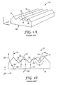
- FIGS. 1A and 1B generally illustrate the concept of structured optical films.
- FIG. 1A shows a perspective view
- FIG. 1B shows a cross-section view of a regular, periodic structured optical film 10 including structured surface 12 and planar surface 14.
- Structured surface 12 includes a series of regularly spaced prisms 16 defined by facets 18 which form peaks 19.
- Prisms 16 have an included angle ⁇ P (that is, the angle formed by facets 18).
- ⁇ P is 90°, which allows for high optical gain.
- each prism 16 extends substantially uninterrupted across the structured surface along the length of its peak 19 (i.e., along the Z-axis).
- Optical film 10 is typically incorporated into an optical system including a backlight assembly which provides light to optical film 10.
- Light rays 20, 22, and 24 are shown in FIG. 1 to depict the behavior of light entering optical film 10 at various angles.
- Light rays 20 and 22 are shown in FIG. 1B to depict the desired operation of a structured optical film.
- Light ray 20 is refracted through the facet within the preferred range of angles relative to film normal N.
- Light ray 22 which also is shown after entering optical film 10 via refraction through planar surface 14, depicts the situation in which a light ray strikes the two facets 18 of a prism 16 above the critical angle required for TIR of the light ray to occur.
- light ray 22 which would have exited structured optical film 10 outside of the preferred range of angles, is reflected back toward the backlight assembly where a portion of it can be "recycled” and returned back to the structured film at an angle that allows it to escape from structured optical film 10.
- the present invention provides a structured optical film wherein these high angle (e.g., angles greater than 60°) light rays are recaptured and redirected back toward the backlight assembly where a portion can be "recycled” and returned back to the structured film at an angle that allows it to escape from structured optical film at a more desirable angle. This can improve contrast and increase brightness of the display at preferred viewing angles.
- these high angle e.g., angles greater than 60°
- FIG. 2A is a perspective view and FIGS. 2B and 2C are partial cross-section views of structured optical film 30 according to an embodiment of the present invention.
- Structured optical film 30 includes structured surface 32 and planar surface 34.
- Structured surface 32 is formed on and planar surface 34 is defined by substrate 35.
- Structured surface 32 includes a plurality of prisms 36 and a plurality of prisms 38 arranged in a periodic pattern. As can be seen in FIG. 2A , prisms 36 and 38 extend substantially uninterrupted across structured surface 32 along the length of their peak (i.e., along the Z-axis).
- the geometry of structured surface 32 and the material used to manufacture film 30 foster total internal reflection (TIR) and refraction of light entering planar side 34 of film 30 and light transmitted from structured surface 32 at high glancing angles to minimize the escape of light through the structured surface outside of a desired range of angles relative to film normal N.
- TIR total internal reflection
- FIG. 2B is a partial cross-section view of structured optical film 30, showing various parameters of structured optical film 30.
- Prisms 36 have a first height h 1 and prisms 38 have a second height h 2 greater than first height h 1 (h 2 > h 1 ).
- first height h 1 is less than 30% height h 2 .
- First height h 1 is preferably in the range of about 5 ⁇ m to about 20 ⁇ m
- second height h 2 is preferably in the range of about 20 ⁇ m to about 50 ⁇ m.
- h 1 and h 2 are chosen such that a light ray escaping from the peak of a prism 36 at an angle of 75° from the normal to the film will be intercepted by one of the prisms 38.
- h 2 would generally be at least one and a half times as great as h 1 although smaller ratios may work depending on design of structured surface 32.
- h 2 is at least twice as great as h 1 and even more preferably h 2 is at least three times as great as h 1 .
- prisms 36 should be at least large enough that diffractive effects do not introduce undesirable color and prisms 38 should not be large enough to be visible to a user through the lcd panel with which the film is used.
- Each prism 36 includes two facets which define an included angle ⁇ S .
- Included angle ⁇ S is preferably about 90°, which allows for maximum optical gain from light supplied by the backlight assembly.
- “Gain” refers to the ratio of the on-axis brightness (that is, the brightness in a direction normal to the display) of a backlit display equipped with a brightness enhancing film to the perpendicular brightness of the display in the absence of the film.
- Prisms 38 preferably include a peak and a base.
- the peak of prisms 38 is defined by a first pair of peak facets 40 and 42, which has an included angle ⁇ P (that is, the angle formed by peak facets 40 and 42). Included angle ⁇ P is preferably in the range of about 70° to about 110°.
- the base of prisms 38 is defined by a second pair of base facets 44 and 46, which has included angle of ⁇ B (that is, the angle at which base facets 44 and 46 are positioned with respect to each other). Included angle ⁇ B is preferably about 90°.
- each prism 38 The peak and the base of each prism 38 are preferably integral with each other.
- Prisms 38 have a truncation height h t , which is the height at which the base facets 44 and 46 meet peak facets 40 and 42.
- truncation height h t and height h i of prisms 36 are substantially similar.
- prisms 38 have width w L and prisms 36 have a width w S . As shown in FIG. 2B , width w L is larger than width w S (w L > w S ). Preferably, width w S is less than 30% width w L .
- Width w S is preferably in the range of 10 ⁇ m to about 40 ⁇ m, and width w L is preferably in the range of about 40 ⁇ m to about 100 ⁇ m.
- Unit cell pitch P UC is the width of a repeating unit of prisms (i.e., a unit cell) in optical film 30.
- a unit cell includes three prisms 36 and one prism 38.
- Peak facets 40 and 42 of prisms 38 meet to form peak tip 48.
- Peak tip 48 is shown in FIGS. 2A-2C having a rounded or blunted contour.
- the rounded contour is characterized by radius of curvature r C .
- Radius of curvature r C is preferably less than 10.5 ⁇ m, and most preferably radius of curvature r C is about 6 ⁇ m. While rounding peak tips 48 results in a decrease of gain in prisms 38, scratching caused by breaking or marring of peak tips 48 during handling and use is prevented.
- prisms 38 are taller than prisms 36, the peaks of prisms 36 are protected from damage during handling and use. This allows prisms 36 to have sharp peaks to maximize gain of prisms 36.
- prisms 38 may have sharp peak tips 48 (i.e., radius of curvature r C of zero) to maximize gain of prisms 38.
- FIG. 2C is a partial cross-section view of structured optical film 30, showing the behavior of light rays entering the structured optical film at various angles.
- Optical film 30 is typically incorporated into an optical system including a backlight assembly which provides light to optical film 30.
- Light rays 50, 52, and 54 are shown in FIG. 2C to depict the behavior of light entering optical film 30 at various angles.
- Light ray 50 which is shown after entering optical film 30 via refraction through planar surface 34, depicts the situation in which a light ray reaches prism 16 below the critical angle required for TIR. Light ray 50 is refracted through the facet within the preferred range of angles relative to film normal N.
- Light ray 52 which also is shown after entering optical film 30 via refraction through planar surface 34, depicts the situation in which a light ray prism 16 above the critical angle required for TIR of the light ray to occur.
- light ray 50 which would have exited structured optical film 30 outside of the preferred range of angles, is reflected back toward the backlight assembly where a portion of it can be "recycled” and returned back to the structured film at an angle that allows it to escape from structured optical film 30.
- Light ray 54 is shown after entering structured optical film 30 via refraction through planar surface 34 and depicts the situation in which a light ray is allowed to escape from prisms 36 at high glancing angles. This is the undesirable situation described with regard to light ray 24 of FIG. 1B .
- light ray 54 is reflected by TIR from a first facet to a second facet of a prism 36.
- Light ray 54 contacts the second facet below the critical angle required for TIR of light ray 54 by the second facet.
- the second facet consequently refracts light ray 54, which escapes structured optical film 30 outside of the desired range of angles.
- high angle light rays are reduced in two regards.
- high angle light rays transmitted by prisms 36 e.g., light ray 54
- prisms 38 each prism 38 is shaped such that light distributed in high angle lobes by prisms 36 is captured and redirected by prism 38 to be eventually reflected back toward the backlight assembly.
- Light ray 54 is reflected via TIR by the various surfaces of optical film 30 until it reaches the backlight assembly.
- prisms 38 have included angles ⁇ P and ⁇ B such that light rays that reach prisms 38 directly from the backlight assembly at undesirable angles are more likely to be reflected via TIR back toward the backlight assembly, rather than being transmitted from optical film 30 at a high glancing angle. In both cases, upon reaching the backlight assembly a portion of the light is "recycled" and returned back to structured film 30 at an angle that allows it to escape from structured optical film 30 at a more desirable angle.
- angle ⁇ p formed by facets 40 and 42 is preferably in the range of about 70° to about 110°, and more preferably in the range of about 90° to about 110° (with an angle of about 96° most preferred). Facets 40 and 42 positioned at these preferred angles with respect to each other produce the greatest likelihood of recapture of high angle light rays. Furthermore, facets 40 and 42 are positioned at these preferred angles to minimize escape of light rays from prisms 38 in high angle lobes.
- intensity of light at angles greater than 75° from normal N is substantially eliminated. In particular, in a system including optical film 30 according to the present invention, light intensity at angles greater than about 75° from normal N are less than about 10% the light intensity along normal N.
- the periodic pattern of prisms 36 and 38 (i.e., the unit cell configuration) as shown in FIGS. 2A-2C is merely exemplary, and other patterns may be used.
- fewer or more prisms 36 may be positioned between prisms 38. While fewer high angle rays are captured with the additional space (i.e., additional prisms 36) between prisms 38, additional prisms 36 allow for an increase in gain, since prisms 36 are shaped to maximize gain.
- larger prisms 38 are interspersed at regular intervals with smaller prisms 36.
- optical film 30 may include only large prisms 38 (that is, no small prisms 36 interspersed between large prisms 38) for a reduction in high angle light rays over conventional films. This is because prisms 38 themselves are shaped to reduce distribution of light rays in high angle lobes.
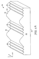
- This embodiment is not covered by the claims, but is depicted in FIG. 3 as optical film 60.
- the parameters described with regard to prisms 38 in optical film 30 are applicable to prisms 38 in optical film 60.
- included angle ⁇ P is preferably greater than 90° (with an angle of about 96° most preferred), to produce a reduction in high angle light rays over conventional films.
- FIG. 3 also shows light ray 70 reaching prism 38 at an undesirable angle and being reflected via TIR back toward the backlight assembly, rather than being transmitted from optical film 60 at a high glancing angle.
- a useful cutting tool for producing such prisms is disclosed in WO 2004/061536 .
- prisms 38 be the same height or that all of prisms 36 be the same height. For various reasons these heights may be varied. However, in order to maximize the effectiveness of the film in enhancing brightness, it is preferred that there be no land spaces between the prisms regardless of whether they are all of the same height or have multiple heights. While it is understood that, at some level of magnification, the valleys between the prisms will be flat or rounded, the term "no land" shall be understood to mean that the valleys are reasonably sharp corners in view of standard machining and molding techniques.
- first height h 1 of prisms 36 and second height h 2 of prisms 38 may be adjusted as system requirements and specifications dictate to adjust gain and recapture of high angle rays.
- first height h 1 of prisms 36 and second height h 2 of prisms 38 may be varied along the length of their peaks (i.e., along the Z-axis).
- prisms 36 and 38 are shown in FIGS. 2A-2C with generally planar facets, but it will be understood that the present invention includes structured optical films having prisms and facets formed in any optically useful shape.
- prisms 36 or 38 may include variations such as rounded valleys, curved facets, etc.
- the present invention is useful with any structured optical film that reduces light distributed in high angle lobes by recapturing and redirecting light for retransmission at more desirable angles.
- structured optical films according to the present invention may vary, it is important that the material be substantially transparent to ensure high optical transmission.
- Useful polymeric materials for this purpose are commercially available such as, for example, acrylics, polycarbonates, acrylate, polyester, polypropylene, polystyrene, polyvinyl chloride, and the like. While the particular material is not critical, materials having higher indices of refraction will generally be preferred. More specifically, materials having indices of refraction greater than 1.5 are most preferable.
- Useful materials for forming structured optical films are discussed in U.S. Pat. Nos. 5,175,030 (Lu et al. ) and 5,183,597 (Lu ).
- a structured surface film according to the present invention may be manufactured by any suitable molding process such as compression molding, injection molding or extrusion or by a cast and cure process such as is described in the Lu patents cited above.
- the substrate on which the structures are formed may be any suitable material such as acrylic, polycarbonate, or polyester.
- the substrate could be a multilayer reflective polarizer or a cholesteric reflective polarizer in order to combine the beneficial effects of a structured surface brightness enhancing film with those of a reflective polarizer.
- a reflective polarizer could be laminated to the films.
- a relatively rigid sheet of plastic or glass could be laminated to the film in order to provide better resistance to warp.
- FIG. 4 illustrates one application in which a layer of structured optical film according to the present invention can be advantageously used.
- the application is a backlit optical display assembly 80.
- Optical display assembly 80 includes a display panel 82 and structured optical film 84 according to the present invention.
- Optical display assembly 80 also includes backlight assembly 86 for use in those situations in which ambient light is insufficient to view display panel 84.
- Backlight assembly 86 is preferably generally wedge-shaped or slab-shaped, but it should be noted that any shape or type of backlight source may be used in place of the backlight assembly pictured including, but not limited to, a direct-lit type assembly (e.g., a direct-lit liquid crystal display (LCD) television), a surface-emission type assembly, a flat edge-lit type assembly, and so on.
- Backlight assembly 86 may be optically coupled to, or integral with, structured optical film 84.
- optical display assembly 80 is shown in its simplest form, and additional optically useful layers may be incorporated into optical display assembly 80 between display panel 82 and structured optical film 84, between structured optical film 84 and backlight assembly 86, and below backlight assembly 86. Examples of such optically useful layers include, but are not limited to, reflective polarizers, diffusers, cover sheets, and reflector layers. These optically useful layers may be optically coupled to, or integral with, structured optical film 84.
- Structured optical film 84 is a conceptual representation of any of the embodiments of the present invention (or variations thereof) heretofore described with regard to FIGS. 2A-2C .
- Structured optical film 84 is preferably positioned between display panel 82 and backlight assembly 86 with the structured surface facing display panel 82 and the planar surface facing backlight assembly 86.
- the larger light directing protrusions 90 of structured optical film 84 redirect light distributed by smaller light directing protrusions 92 in high angle lobes back toward backlight assembly 86.
- the larger light directing protrusions themselves are shaped to reduce distribution of light rays in high angle lobes.
- the redirected light is then "recycled" when it is reflected by backlight assembly 86 toward structured optical film 84 for retransmission to display panel 84 at a more desirable angle. This can improve contrast and increase brightness of the display at preferred viewing angles as a consequence of reducing high angle outputs of the shorter light directing protrusions.
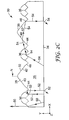
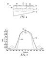
- FIG. 5 shows luminous intensity distribution plot 100 for conventional structured optical film 10 (as shown in FIGS. 1A and 1B ) and luminous intensity distribution plot 110 for structured optical film 30 according to the present invention (as shown in FIGS. 2A-2C ).
- Luminous intensity distribution plots 100 and 110 plot various angles relative to film normal N versus the radiant intensity at these angles in Watts/steradian (W/sr). For the various angles along the horizontal axis in FIG. 5 , 0° is along film normal N (i.e., along the Y-axis in FIGS. 1A, 1B , and 2A-2C ), and ⁇ 90° is perpendicular to film normal N (i.e., along the X-axis in FIGS.
- the radiant intensity for the plots in FIG. 5 is calculated in a system substantially similar to that shown in FIG. 4 , wherein backlight assembly 86 provides a distribution of light and wherewith a radiant intensity detector is positioned on a side opposite of display panel 82 from structured optical film 84.
- the plots represent the calculated radiant intensity of light along the XY-plane in FIGS. 1A, 1B , in 2A-2C at various angles relative to film normal N.
- Luminous intensity distribution plot 100 is shown for structured optical film 10, wherein prisms 16 have an included angle ⁇ S of 90°.
- peak radiant intensity 102 occurs at 0°, or, along normal N of optical film 10.
- the radiant intensity decreases until around ⁇ 45 from normal N.
- light distributed by optical film 10 in high angle lobes e.g., light ray 24 in FIG. 1B
- the increased radiant intensity occurs at angles between about ⁇ 45° to ⁇ 90°.
- the high radiant intensity at these high angles may reduce the contrast of the display and produce undesirable areas of brightness outside of a preferred viewing angle of the display.
- the high angle lobes reduce the light intensity within the preferred viewing angles, since these rays escape structured optical film 10 without being recycled and retransmitted at a preferred viewing angle.
- Luminous intensity distribution plot 110 is shown for structured optical film 30 according to the present invention.
- Plot 110 is for structured optical film 30 including configuration parameters as follows: included angle ⁇ P of 96°, included angles ⁇ B and ⁇ S of 90°, and radius of curvature r C of 6 ⁇ m.
- peak radiant intensity 112 also occurs at 0°, or, along normal N of optical film 30.
- the radiant intensity decreases until about -55° and 55° from normal N.
- the radiant intensity at increasing angles from normal N is substantially constant.
- a small region of increased radiant intensity 114 occurs at angles greater than ⁇ 60° from film normal N due to a small amount of light escaping from optical film 30 at high angles. However, the drop in intensity at these angles is significant over conventional optical film 10.
- a merit function can be defined to demonstrate the advantage of the structured optical film of the present invention over conventional structured optical films.
- the merit function is defined as the ratio of the maximum radiant intensity (at 0°, or, along film normal N) to the radiant intensity at ⁇ 75° (i.e., at high glancing angles).
- the radiant intensity at 0° is 0.2985 W/sr
- the radiant intensity at ⁇ 75° is 0.051 W/sr.
- the radiant intensity at 0° is 0.2953 W/sr
- the radiant intensity at ⁇ 75° is 0.026 W/sr.
- peak radiant intensity 112 is slightly less than peak radiant intensity 102
- the radiant intensity at ⁇ 75° in optical film 30 is nearly half the radiant intensity at ⁇ 75° in optical film.
- the decrease in high angle light rays output from a structured optical film according to the present invention is significant.
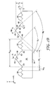
- FIG. 6 is a scatterplot of merit function versus gain of conventional structured optical film 10 and optical film 30 according to the present invention.
- gain refers to the ratio of the on-axis brightness (that is, the brightness in a direction normal to the display) of a backlit display equipped with a brightness enhancing film to the on-axis brightness of the display in the absence of the film.
- conventional structured optical film 10 has an included angle ⁇ P .
- Scatterplot 120 is for optical film 10 having prisms 16 with an included angle ⁇ P of 90° and sharp peaks 19.
- structured optical film 10 with this configuration has a merit function of 5.8529.
- structured optical film 10 with this configuration has a gain of about 1.61. This point is plotted in FIG. 6 as scatterplot 120.
- the remaining scatterplots 125 in FIG. 6 show the merit function versus gain for a structured optical film 30 according to the present invention.
- included angle ⁇ P of structured optical film 30 was varied, which resulted in variations of the merit function and gain of optical film 30.
- Included angle ⁇ S of prisms 36 and included angle ⁇ B of prisms 38 were maintained at 90°, and radius of curvature r C was maintained at 6 ⁇ m.
- the gain is slightly decreased due to the variation of the shape of prisms 38, the increase in merit function is very significant compared to conventional structured optical film 10.
- the relative decrease in radiant intensity at high glancing angles is significant over conventional structured optical film 10 at a minimal loss in gain and in intensity along the film normal. This can improve contrast and increase brightness of the display at preferred viewing angles as a consequence of reducing high angle outputs.
- the present invention is a brightness enhancement article for recycling these high angle light rays back to the structured film for retransmission within the range of desired angles.
- the brightness enhancement article has a structured surface including a plurality of light directing protrusions.
- the structured surface includes a plurality of first light directing protrusions and a plurality of second light directing protrusions.
- Each of the first light directing protrusions has a first height and produces a light distribution having high angle lobes and lobes generally normal to the structured surface.
- the second light directing protrusions are positioned with respect to the first light directing protrusions.
- Each of the second light directing protrusions has a second height greater than the first height and a shape which redirects light distributed by the first light directing protrusions in the high angle lobes.
- the second light directing protrusions have a shape such that light rays that reach the second light directing protrusions directly from the backlight assembly at undesirable angles are more likely to be reflected back toward the backlight assembly, rather than being transmitted from the optical film at a high glancing angle.
Abstract
Description
- The present invention relates to structured optical films and optical displays incorporating the structured optical films. More specifically, the present invention relates to a brightness enhancement film with reduced glancing angle output.
- Electronic devices that include electronic displays for conveying information to a viewer have become nearly ubiquitous. Mobile phones, handheld computers, personal digital assistants, electronic games, car stereos and indicators, public displays, automated teller machines, in-store kiosks, home appliances, computer monitors, televisions, etc., are all examples of devices that include displays that people view on a daily basis.
- The typical electronic display assembly contains a light source that is required in order for people to observe the information presented by the display. In battery powered equipment, the light source can represent a substantial fraction of the total power draw of the equipment. Therefore, reducing the amount of power required to produce a given luminance increases battery life, which is especially desirable in battery powered equipment.
- Structured optical films are used in electronic display systems and in other applications where control over the direction of light, transmitted and/or reflected, is desired to increase brightness, reduce glare, etc. A structured optical film essentially comprises films of light transmissible materials in which a series of prisms are located such that the films can be used to redirect light through reflection and refraction. When used in an optical display such as that found in laptop computers, watches, etc., the structured optical film can increase brightness of an optical display by limiting light escaping from the display to within a pair of planes disposed at desired angles from a normal axis running through the optical display. As a result, light that would exit the display outside of the allowable range is reflected back into the display where a portion of it can be "recycled" and returned back to the structured film at an angle that allows it to escape from the display. That recycling is useful because it can reduce power consumption needed to provide a display with a desired level of brightness.
- In conventional structured optical films, some light is allowed to exit the display outside the allowable range of angles relative to the normal axis running through the display. These high angle light rays may reduce the contrast of the display (the difference in brightness between light and dark areas of the display) and produce undesirable areas of brightness outside of a preferred viewing angle. It would be desirable to recycle these high angle light rays and return them back to the structured film for retransmission within the range of desired angles.
WO 2004/061536 discloses a cutting tool for producing a brightness enhancement article as recited in the pre-characterising portion of claim 1. - The present invention is a brightness enhancement article as recited in claim 1.
- Preferably, the first included angle of the first light directing protrusions is greater than 90° and the second included angle of the second light directing protrusions is about 90°. Furthermore, the peak of the first light directing protrusions preferably has a rounded peak having a radius of curvature of less than about 10.5 µm. Also, at least one second light directing protrusion is positioned between adjacent first light directing protrusions.
- The brightness enhancement article of the present invention is typically incorporated in a display module. The display module typically includes a display panel and a backlight assembly for providing light to the display panel. The brightness enhancement article is located between the backlight assembly and the display panel, with the structured surface facing the display panel.
-
-
FIG. 1A is a perspective view of a conventional structured optical film. -
FIG. 1B is a cross-section view of the conventional structured optical film ofFIG. 1A . -
FIG. 2A is a perspective view of a structured optical film according to the present invention. -
FIG. 2B is a partial cross-section view of the structured optical film ofFIG. 2A , showing various parameters of the structured optical film. -
FIG. 2C is a partial cross-section view of the structured optical film ofFIG. 2A , showing the behavior of light rays entering the structured optical film at various angles. -
FIG. 3 is a partial cross-section view of a structured optical film according to another embodiment for which no protection is sought. -
FIG. 4 is a cross-section view of an optical display assembly incorporating a structured optical film according to the present invention. -
FIG. 5 is a luminous intensity distribution plot for the conventional structured optical film ofFIGS. 1A and 1B , and for the structured optical film according to the present invention shown inFIGS. 2A-2C . -
FIG. 6 is a scatter plot of merit function versus gain of a conventional structured optical film and an optical film according to the present invention. -
FIGS. 1A and 1B generally illustrate the concept of structured optical films.FIG. 1A shows a perspective view andFIG. 1B shows a cross-section view of a regular, periodic structuredoptical film 10 including structuredsurface 12 andplanar surface 14.Structured surface 12 includes a series of regularly spacedprisms 16 defined byfacets 18 which formpeaks 19.Prisms 16 have an included angle αP (that is, the angle formed by facets 18). Typically, αP is 90°, which allows for high optical gain. As can be seen, eachprism 16 extends substantially uninterrupted across the structured surface along the length of its peak 19 (i.e., along the Z-axis). -
Optical film 10 is typically incorporated into an optical system including a backlight assembly which provides light tooptical film 10.Light rays FIG. 1 to depict the behavior of light enteringoptical film 10 at various angles.Light rays FIG. 1B to depict the desired operation of a structured optical film.Light ray 20, which is shown after enteringoptical film 10 via refraction throughplanar surface 14, depicts the situation in which a light ray contacts afacet 18 ofprism 16 below the critical angle required for TIR.Light ray 20 is refracted through the facet within the preferred range of angles relative to film normal N. -
Light ray 22, which also is shown after enteringoptical film 10 via refraction throughplanar surface 14, depicts the situation in which a light ray strikes the twofacets 18 of aprism 16 above the critical angle required for TIR of the light ray to occur. As a result,light ray 22, which would have exited structuredoptical film 10 outside of the preferred range of angles, is reflected back toward the backlight assembly where a portion of it can be "recycled" and returned back to the structured film at an angle that allows it to escape from structuredoptical film 10. - With conventional structured optical film designs, some light is allowed to escape from
prisms 16 at high glancing angles. This situation is depicted bylight ray 24. The escape of light usually occurs whenlight ray 24 is reflected by TIR from a first facet to a second facet of aprism 16, andlight ray 24 contacts the second facet below the critical angle required for TIR oflight ray 24 by the second facet. The second facet consequently refractslight ray 24, which escapes structuredoptical film 10 outside of the preferred range of angles. These high angle light rays may reduce the contrast of the display and produce undesirable areas of brightness outside of the preferred viewing angles of the display (e.g., within 30° of optical film normal N). - The present invention, described in connection with the illustrative embodiments depicted in
FIG. 2A and the following figures, provides a structured optical film wherein these high angle (e.g., angles greater than 60°) light rays are recaptured and redirected back toward the backlight assembly where a portion can be "recycled" and returned back to the structured film at an angle that allows it to escape from structured optical film at a more desirable angle. This can improve contrast and increase brightness of the display at preferred viewing angles. -
FIG. 2A is a perspective view andFIGS. 2B and2C are partial cross-section views of structuredoptical film 30 according to an embodiment of the present invention. Structuredoptical film 30 includes structuredsurface 32 andplanar surface 34. Structuredsurface 32 is formed on andplanar surface 34 is defined bysubstrate 35. Structuredsurface 32 includes a plurality ofprisms 36 and a plurality ofprisms 38 arranged in a periodic pattern. As can be seen inFIG. 2A ,prisms surface 32 along the length of their peak (i.e., along the Z-axis). The geometry of structuredsurface 32 and the material used to manufacturefilm 30 foster total internal reflection (TIR) and refraction of light enteringplanar side 34 offilm 30 and light transmitted from structuredsurface 32 at high glancing angles to minimize the escape of light through the structured surface outside of a desired range of angles relative to film normal N. -
FIG. 2B is a partial cross-section view of structuredoptical film 30, showing various parameters of structuredoptical film 30.Prisms 36 have a first height h1 andprisms 38 have a second height h2 greater than first height h1 (h2 > h1). Preferably, first height h1 is less than 30% height h2. First height h1 is preferably in the range of about 5 µm to about 20 µm, and second height h2 is preferably in the range of about 20 µm to about 50 µm. Preferably h1 and h2 are chosen such that a light ray escaping from the peak of aprism 36 at an angle of 75° from the normal to the film will be intercepted by one of theprisms 38. It is expected that h2 would generally be at least one and a half times as great as h1 although smaller ratios may work depending on design of structuredsurface 32. Preferably h2 is at least twice as great as h1 and even more preferably h2 is at least three times as great as h1. For cosmetic reasons,prisms 36 should be at least large enough that diffractive effects do not introduce undesirable color andprisms 38 should not be large enough to be visible to a user through the lcd panel with which the film is used. - Each
prism 36 includes two facets which define an included angle θS. Included angle θS is preferably about 90°, which allows for maximum optical gain from light supplied by the backlight assembly. "Gain" refers to the ratio of the on-axis brightness (that is, the brightness in a direction normal to the display) of a backlit display equipped with a brightness enhancing film to the perpendicular brightness of the display in the absence of the film. -
Prisms 38 preferably include a peak and a base. The peak ofprisms 38 is defined by a first pair ofpeak facets peak facets 40 and 42). Included angle θP is preferably in the range of about 70° to about 110°. The base ofprisms 38 is defined by a second pair ofbase facets base facets - The peak and the base of each
prism 38 are preferably integral with each other.Prisms 38 have a truncation height ht, which is the height at which thebase facets meet peak facets prisms 36 are substantially similar. Furthermore,prisms 38 have width wL andprisms 36 have a width wS. As shown inFIG. 2B , width wL is larger than width wS (wL > wS). Preferably, width wS is less than 30% width wL. Width wS is preferably in the range of 10 µm to about 40 µm, and width wL is preferably in the range of about 40 µm to about 100 µm. Unit cell pitch PUC is the width of a repeating unit of prisms (i.e., a unit cell) inoptical film 30. In the embodiment shown inFIG. 2B , a unit cell includes threeprisms 36 and oneprism 38. -
Peak facets prisms 38 meet to formpeak tip 48.Peak tip 48 is shown inFIGS. 2A-2C having a rounded or blunted contour. The rounded contour is characterized by radius of curvature rC. Radius of curvature rC is preferably less than 10.5 µm, and most preferably radius of curvature rC is about 6 µm. While roundingpeak tips 48 results in a decrease of gain inprisms 38, scratching caused by breaking or marring ofpeak tips 48 during handling and use is prevented. Furthermore, becauseprisms 38 are taller thanprisms 36, the peaks ofprisms 36 are protected from damage during handling and use. This allowsprisms 36 to have sharp peaks to maximize gain ofprisms 36. Alternatively, if scratchingoptical film 30 can be avoided,prisms 38 may have sharp peak tips 48 (i.e., radius of curvature rC of zero) to maximize gain ofprisms 38. -
FIG. 2C is a partial cross-section view of structuredoptical film 30, showing the behavior of light rays entering the structured optical film at various angles.Optical film 30 is typically incorporated into an optical system including a backlight assembly which provides light tooptical film 30. Light rays 50, 52, and 54 are shown inFIG. 2C to depict the behavior of light enteringoptical film 30 at various angles. -
Light ray 50, which is shown after enteringoptical film 30 via refraction throughplanar surface 34, depicts the situation in which a light ray reachesprism 16 below the critical angle required for TIR.Light ray 50 is refracted through the facet within the preferred range of angles relative to film normal N. -
Light ray 52, which also is shown after enteringoptical film 30 via refraction throughplanar surface 34, depicts the situation in which alight ray prism 16 above the critical angle required for TIR of the light ray to occur. As a result,light ray 50, which would have exited structuredoptical film 30 outside of the preferred range of angles, is reflected back toward the backlight assembly where a portion of it can be "recycled" and returned back to the structured film at an angle that allows it to escape from structuredoptical film 30. -
Light ray 54 is shown after entering structuredoptical film 30 via refraction throughplanar surface 34 and depicts the situation in which a light ray is allowed to escape fromprisms 36 at high glancing angles. This is the undesirable situation described with regard tolight ray 24 ofFIG. 1B . To recapitulate,light ray 54 is reflected by TIR from a first facet to a second facet of aprism 36.Light ray 54 contacts the second facet below the critical angle required for TIR oflight ray 54 by the second facet. The second facet consequently refractslight ray 54, which escapes structuredoptical film 30 outside of the desired range of angles. - In structured
optical film 30 according to the present invention, high angle light rays are reduced in two regards. First, high angle light rays transmitted by prisms 36 (e.g., light ray 54) are recaptured byprisms 38. That is, eachprism 38 is shaped such that light distributed in high angle lobes byprisms 36 is captured and redirected byprism 38 to be eventually reflected back toward the backlight assembly.Light ray 54 is reflected via TIR by the various surfaces ofoptical film 30 until it reaches the backlight assembly. Second,prisms 38 have included angles θP and θB such that light rays that reachprisms 38 directly from the backlight assembly at undesirable angles are more likely to be reflected via TIR back toward the backlight assembly, rather than being transmitted fromoptical film 30 at a high glancing angle. In both cases, upon reaching the backlight assembly a portion of the light is "recycled" and returned back to structuredfilm 30 at an angle that allows it to escape from structuredoptical film 30 at a more desirable angle. - In order to facilitate the recapture and recycling of light distributed by
prisms 36 in high angle lobes, angle θp formed byfacets Facets facets prisms 38 in high angle lobes. Inoptical film 30 according to the present invention, intensity of light at angles greater than 75° from normal N is substantially eliminated. In particular, in a system includingoptical film 30 according to the present invention, light intensity at angles greater than about 75° from normal N are less than about 10% the light intensity along normal N. - The periodic pattern of
prisms 36 and 38 (i.e., the unit cell configuration) as shown inFIGS. 2A-2C is merely exemplary, and other patterns may be used. For example, fewer ormore prisms 36 may be positioned betweenprisms 38. While fewer high angle rays are captured with the additional space (i.e., additional prisms 36) betweenprisms 38,additional prisms 36 allow for an increase in gain, sinceprisms 36 are shaped to maximize gain. In general,larger prisms 38 are interspersed at regular intervals withsmaller prisms 36. - It is also important to note that
optical film 30 may include only large prisms 38 (that is, nosmall prisms 36 interspersed between large prisms 38) for a reduction in high angle light rays over conventional films. This is becauseprisms 38 themselves are shaped to reduce distribution of light rays in high angle lobes. This embodiment is not covered by the claims, but is depicted inFIG. 3 asoptical film 60. In general, the parameters described with regard toprisms 38 inoptical film 30 are applicable toprisms 38 inoptical film 60. However, for this embodiment, included angle θP is preferably greater than 90° (with an angle of about 96° most preferred), to produce a reduction in high angle light rays over conventional films.FIG. 3 also showslight ray 70 reachingprism 38 at an undesirable angle and being reflected via TIR back toward the backlight assembly, rather than being transmitted fromoptical film 60 at a high glancing angle. A useful cutting tool for producing such prisms is disclosed inWO 2004/061536 . - Furthermore it is not necessary that all of
prisms 38 be the same height or that all ofprisms 36 be the same height. For various reasons these heights may be varied. However, in order to maximize the effectiveness of the film in enhancing brightness, it is preferred that there be no land spaces between the prisms regardless of whether they are all of the same height or have multiple heights. While it is understood that, at some level of magnification, the valleys between the prisms will be flat or rounded, the term "no land" shall be understood to mean that the valleys are reasonably sharp corners in view of standard machining and molding techniques. - It should also be noted that various parameters of
prisms prisms 36 and second height h2 ofprisms 38 may be adjusted as system requirements and specifications dictate to adjust gain and recapture of high angle rays. Also, first height h1 ofprisms 36 and second height h2 ofprisms 38 may be varied along the length of their peaks (i.e., along the Z-axis). Furthermore,prisms FIGS. 2A-2C with generally planar facets, but it will be understood that the present invention includes structured optical films having prisms and facets formed in any optically useful shape. For example,prisms - Although the particular material used to manufacture structured optical films according to the present invention may vary, it is important that the material be substantially transparent to ensure high optical transmission. Useful polymeric materials for this purpose are commercially available such as, for example, acrylics, polycarbonates, acrylate, polyester, polypropylene, polystyrene, polyvinyl chloride, and the like. While the particular material is not critical, materials having higher indices of refraction will generally be preferred. More specifically, materials having indices of refraction greater than 1.5 are most preferable. Useful materials for forming structured optical films are discussed in
U.S. Pat. Nos. 5,175,030 (Lu et al. ) and5,183,597 (Lu ). - A structured surface film according to the present invention may be manufactured by any suitable molding process such as compression molding, injection molding or extrusion or by a cast and cure process such as is described in the Lu patents cited above. If the film is manufactured by a cast and cure process the substrate on which the structures are formed may be any suitable material such as acrylic, polycarbonate, or polyester. In another embodiment, the substrate could be a multilayer reflective polarizer or a cholesteric reflective polarizer in order to combine the beneficial effects of a structured surface brightness enhancing film with those of a reflective polarizer. Alternatively, regardless of the manufacturing method, a reflective polarizer could be laminated to the films. Furthermore, with or without a reflective polarizer, a relatively rigid sheet of plastic or glass could be laminated to the film in order to provide better resistance to warp.
-
FIG. 4 illustrates one application in which a layer of structured optical film according to the present invention can be advantageously used. The application is a backlitoptical display assembly 80.Optical display assembly 80 includes adisplay panel 82 and structuredoptical film 84 according to the present invention.Optical display assembly 80 also includesbacklight assembly 86 for use in those situations in which ambient light is insufficient to viewdisplay panel 84.Backlight assembly 86 is preferably generally wedge-shaped or slab-shaped, but it should be noted that any shape or type of backlight source may be used in place of the backlight assembly pictured including, but not limited to, a direct-lit type assembly (e.g., a direct-lit liquid crystal display (LCD) television), a surface-emission type assembly, a flat edge-lit type assembly, and so on.Backlight assembly 86 may be optically coupled to, or integral with, structuredoptical film 84. Furthermore,optical display assembly 80 is shown in its simplest form, and additional optically useful layers may be incorporated intooptical display assembly 80 betweendisplay panel 82 and structuredoptical film 84, between structuredoptical film 84 andbacklight assembly 86, and belowbacklight assembly 86. Examples of such optically useful layers include, but are not limited to, reflective polarizers, diffusers, cover sheets, and reflector layers. These optically useful layers may be optically coupled to, or integral with, structuredoptical film 84. - Structured
optical film 84 is a conceptual representation of any of the embodiments of the present invention (or variations thereof) heretofore described with regard toFIGS. 2A-2C . Structuredoptical film 84 is preferably positioned betweendisplay panel 82 andbacklight assembly 86 with the structured surface facingdisplay panel 82 and the planar surface facingbacklight assembly 86. The largerlight directing protrusions 90 of structuredoptical film 84 redirect light distributed by smallerlight directing protrusions 92 in high angle lobes back towardbacklight assembly 86. Furthermore, the larger light directing protrusions themselves are shaped to reduce distribution of light rays in high angle lobes. The redirected light is then "recycled" when it is reflected bybacklight assembly 86 toward structuredoptical film 84 for retransmission to displaypanel 84 at a more desirable angle. This can improve contrast and increase brightness of the display at preferred viewing angles as a consequence of reducing high angle outputs of the shorter light directing protrusions. -
FIG. 5 shows luminousintensity distribution plot 100 for conventional structured optical film 10 (as shown inFIGS. 1A and 1B ) and luminousintensity distribution plot 110 for structuredoptical film 30 according to the present invention (as shown inFIGS. 2A-2C ). Luminousintensity distribution plots FIG. 5 , 0° is along film normal N (i.e., along the Y-axis inFIGS. 1A, 1B , and2A-2C ), and ±90° is perpendicular to film normal N (i.e., along the X-axis inFIGS. 1A, 1B , and2A-2C ). The radiant intensity for the plots inFIG. 5 is calculated in a system substantially similar to that shown inFIG. 4 , whereinbacklight assembly 86 provides a distribution of light and wherewith a radiant intensity detector is positioned on a side opposite ofdisplay panel 82 from structuredoptical film 84. The plots represent the calculated radiant intensity of light along the XY-plane inFIGS. 1A, 1B , in 2A-2C at various angles relative to film normal N. - Luminous
intensity distribution plot 100 is shown for structuredoptical film 10, whereinprisms 16 have an included angle θS of 90°. As shown byplot 100, peakradiant intensity 102 occurs at 0°, or, along normal N ofoptical film 10. At increasing angles from optical film normal N, the radiant intensity decreases until around ±45 from normal N. At this point, light distributed byoptical film 10 in high angle lobes (e.g.,light ray 24 inFIG. 1B ) produces areas of increased light intensity outside of preferred viewing angles. As shown byplot 100, the increased radiant intensity occurs at angles between about ±45° to ±90°. The high radiant intensity at these high angles may reduce the contrast of the display and produce undesirable areas of brightness outside of a preferred viewing angle of the display. Furthermore, the high angle lobes reduce the light intensity within the preferred viewing angles, since these rays escape structuredoptical film 10 without being recycled and retransmitted at a preferred viewing angle. - Luminous
intensity distribution plot 110 is shown for structuredoptical film 30 according to the present invention.Plot 110 is for structuredoptical film 30 including configuration parameters as follows: included angle θP of 96°, included angles θB and θS of 90°, and radius of curvature rC of 6 µm. As shown byplot 110, peakradiant intensity 112 also occurs at 0°, or, along normal N ofoptical film 30. At increasing angles from optical film normal N, the radiant intensity decreases until about -55° and 55° from normal N. At this point, the radiant intensity at increasing angles from normal N is substantially constant. A small region of increased radiant intensity 114 occurs at angles greater than ±60° from film normal N due to a small amount of light escaping fromoptical film 30 at high angles. However, the drop in intensity at these angles is significant over conventionaloptical film 10. - For comparison, a merit function can be defined to demonstrate the advantage of the structured optical film of the present invention over conventional structured optical films. The merit function is defined as the ratio of the maximum radiant intensity (at 0°, or, along film normal N) to the radiant intensity at ±75° (i.e., at high glancing angles). As shown in
FIG. 5 , for conventional structured optical film 10 (plot 100), the radiant intensity at 0° is 0.2985 W/sr, and the radiant intensity at ±75° is 0.051 W/sr. Thus, the merit function is (0.2985 W/sr)/(0.051 W/sr) = 5.8529. - For structured optical 30 according to the present invention (plot 110), the radiant intensity at 0° is 0.2953 W/sr, and the radiant intensity at ±75° is 0.026 W/sr. Thus, the merit function is (0.2953 W/sr)/(0.026 W/sr) = 11.358. While peak
radiant intensity 112 is slightly less than peakradiant intensity 102, the radiant intensity at ±75° inoptical film 30 is nearly half the radiant intensity at ±75° in optical film. Thus, the decrease in high angle light rays output from a structured optical film according to the present invention is significant. - For further comparison,
FIG. 6 is a scatterplot of merit function versus gain of conventional structuredoptical film 10 andoptical film 30 according to the present invention. As stated above, gain refers to the ratio of the on-axis brightness (that is, the brightness in a direction normal to the display) of a backlit display equipped with a brightness enhancing film to the on-axis brightness of the display in the absence of the film. - As described with regard to
FIGS. 1A and 1B , conventional structuredoptical film 10 has an included angle αP.Scatterplot 120 is foroptical film 10 havingprisms 16 with an included angle αP of 90° andsharp peaks 19. As determined above, structuredoptical film 10 with this configuration has a merit function of 5.8529. Furthermore, structuredoptical film 10 with this configuration has a gain of about 1.61. This point is plotted inFIG. 6 asscatterplot 120. - The remaining
scatterplots 125 inFIG. 6 show the merit function versus gain for a structuredoptical film 30 according to the present invention. To producescatterplots 125, included angle θP of structuredoptical film 30 was varied, which resulted in variations of the merit function and gain ofoptical film 30. Included angle θS ofprisms 36 and included angle θB ofprisms 38 were maintained at 90°, and radius of curvature rC was maintained at 6 µm. As can be seen, while the gain is slightly decreased due to the variation of the shape ofprisms 38, the increase in merit function is very significant compared to conventional structuredoptical film 10. In other words, the relative decrease in radiant intensity at high glancing angles (i.e., at angles greater than ±75°) is significant over conventional structuredoptical film 10 at a minimal loss in gain and in intensity along the film normal. This can improve contrast and increase brightness of the display at preferred viewing angles as a consequence of reducing high angle outputs. - In summary, conventional optical films allow some light to exit an optical display outside the allowable range of angles relative to the normal axis running through the display. These high angle light rays produce undesirable areas of brightness outside of a preferred viewing angle that detract from potential additional brightness within the preferred viewing angle and may reduce the contrast of the display. The present invention is a brightness enhancement article for recycling these high angle light rays back to the structured film for retransmission within the range of desired angles. The brightness enhancement article has a structured surface including a plurality of light directing protrusions. Preferably, the structured surface includes a plurality of first light directing protrusions and a plurality of second light directing protrusions. Each of the first light directing protrusions has a first height and produces a light distribution having high angle lobes and lobes generally normal to the structured surface. The second light directing protrusions are positioned with respect to the first light directing protrusions. Each of the second light directing protrusions has a second height greater than the first height and a shape which redirects light distributed by the first light directing protrusions in the high angle lobes. Furthermore, the second light directing protrusions have a shape such that light rays that reach the second light directing protrusions directly from the backlight assembly at undesirable angles are more likely to be reflected back toward the backlight assembly, rather than being transmitted from the optical film at a high glancing angle.
- Although the present invention has been described with reference to preferred embodiments, workers skilled in the art will recognize that changes may be made in form and detail without departing from the scope of the invention.
Claims (11)
- A brightness enhancement article (84) for use in an optical system, the brightness enhancement article having a structured surface (32) comprising:a plurality of first light directing protrusions (38), the first light directing protrusions (38) each including a peak and a base, the peak being defined by a first pair of prism facets (40,42) and the base being defined by a second pair of prism facets (44,46), wherein the first pair of prism facets (40,42) encloses a first included angle (θP) and the second pair of prism facets (44,46) encloses a second included angle (θB), wherein the first included angle (θP) is different from the second included angle (θB); and wherein the tip (48) of the peak has a rounded contour,
characterised bya plurality of second light directing protrusions (36) of lesser height (h1) than the height (h2) of the first light directing protrusions (38), the second light directing protrusions (36) being interleaved with the first light directing protrusions (38) and being arranged to produce a light distribution having high angle lobes and lobes at preferred angles relative to the normal of the structured surface (32), the structured surface (32) being arranged so that light distributed by the second light directing protrusions (36) in the high angle lobes is redirected by the first light directing protrusions (38) for retransmission at a preferred angle. - The brightness enhancement article (84) of claim 1, wherein the second light directing protrusions (36) are interleaved periodically with the first light directing protrusion (38).
- The brightness enhancement article (84) of claim 1, wherein at least one second light directing protrusion (36) is positioned between adjacent first light directing protrusions (38).
- The brightness enhancement article (84) of claim 1, wherein the first included angle (θP) is greater than 90° and the second included angle (θB) is about 90°.
- The brightness enhancement article (84) of claim 1, wherein each of the second light directing protrusions (36) includes a peak defined by two prism facets enclosing an included angle (θS) of about 90°.
- The brightness enhancement article (84) of claim 1, wherein a truncation height (ht) of the second pair of prism facets (44,46) is substantially similar to the height (h1) of the plurality of second light directing protrusions (36).
- The brightness enhancement article (84) of claim 1, wherein the structured surface (32) is made of a material with a refractive index greater than 1.5.
- The brightness enhancement article (84) of claim 1 wherein the first protrusions (38) have heights (h2) at least 1.5 times the height (h1) of the second protrusions.
- The brightness enhancement article (84) of claim 8 wherein the first protrusions (38) have heights (h2) at least twice times the heights (h1) of the second protrusions (36).
- The brightness enhancement article (84) of claim 9 wherein the first protrusions (38) have heights (h2) at least three times the heights (h1) of the second protrusions (36).
- An optical display assembly (80) comprising:a display panel (82);a backlight assembly (86); anda brightness enhancement article (84) according to claim 1 positioned between the backlight assembly (86) and the display panel (82) with the structured surface (32) facing the display panel (82).
Applications Claiming Priority (2)
| Application Number | Priority Date | Filing Date | Title |
|---|---|---|---|
| US11/027,172 US7384173B2 (en) | 2004-12-30 | 2004-12-30 | Brightness enhancement article |
| PCT/US2005/043738 WO2006073644A1 (en) | 2004-12-30 | 2005-12-01 | Brightness enhancement article |
Publications (2)
| Publication Number | Publication Date |
|---|---|
| EP1831754A1 EP1831754A1 (en) | 2007-09-12 |
| EP1831754B1 true EP1831754B1 (en) | 2008-12-31 |
Family
ID=36168575
Family Applications (1)
| Application Number | Title | Priority Date | Filing Date |
|---|---|---|---|
| EP05852845A Not-in-force EP1831754B1 (en) | 2004-12-30 | 2005-12-01 | Brightness enhancement article |
Country Status (9)
| Country | Link |
|---|---|
| US (1) | US7384173B2 (en) |
| EP (1) | EP1831754B1 (en) |
| JP (1) | JP2008527409A (en) |
| KR (1) | KR20070090981A (en) |
| CN (1) | CN101095076A (en) |
| AT (1) | ATE419555T1 (en) |
| DE (1) | DE602005012150D1 (en) |
| TW (1) | TW200628928A (en) |
| WO (1) | WO2006073644A1 (en) |
Families Citing this family (67)
| Publication number | Priority date | Publication date | Assignee | Title |
|---|---|---|---|---|
| US7859759B2 (en) * | 2002-05-20 | 2010-12-28 | Sabic Innovative Plastics Ip B.V. | Film, backlight displays, and methods for making the same |
| US6952627B2 (en) * | 2002-12-18 | 2005-10-04 | General Electric Company | Method and apparatus for fabricating light management substrates |
| US7800301B2 (en) * | 2004-09-06 | 2010-09-21 | Fujifilm Corporation | Organic electroluminescent device comprising a prism structure |
| KR20060085756A (en) * | 2005-01-25 | 2006-07-28 | 삼성전자주식회사 | Back light assembly, method of manufacturing the same and liquid crystal display device having the same |
| TWI351550B (en) * | 2005-06-09 | 2011-11-01 | Ubright Optronics Corp | Optical substrate |
| KR101158893B1 (en) * | 2005-06-09 | 2012-06-25 | 삼성전자주식회사 | Optical member, backlight assembly having the same and liquid crystal display device having the same |
| EP1826607B1 (en) * | 2006-02-27 | 2010-08-04 | The Swatch Group Research and Development Ltd. | Liquid crystal display device displaying coloured segments and timepiece equipped with such a device |
| JP5168813B2 (en) * | 2006-04-14 | 2013-03-27 | ソニー株式会社 | Optical sheet, backlight device and liquid crystal display device |
| KR20070103544A (en) * | 2006-04-19 | 2007-10-24 | 삼성전자주식회사 | Liquid crystal display and prism sheet for the same |
| WO2008018570A1 (en) * | 2006-08-09 | 2008-02-14 | Tokyo University Of Science Educational Foundation Administrative Organization | Antireflection structure, process for producing the same and process for producing optical member |
| TWI317025B (en) * | 2006-08-28 | 2009-11-11 | Eternal Chemical Co Ltd | Optical film |
| US8436960B2 (en) * | 2006-11-09 | 2013-05-07 | Sharp Kabushiki Kaisha | Prism sheet and liquid crystal display |
| US7527407B2 (en) * | 2006-11-28 | 2009-05-05 | Gamma Optical Co., Ltd. | Optic film and backlight module using same |
| US20080247065A1 (en) * | 2007-04-06 | 2008-10-09 | 3M Innovative Properties Company | Method of making structured optical films |
| KR100905241B1 (en) * | 2007-04-13 | 2009-07-01 | 엘지전자 주식회사 | Optical film having a plurality of structures and backlight unit including the same |
| US7485026B2 (en) * | 2007-06-13 | 2009-02-03 | Black & Decker Inc. | Sander |
| US7722435B2 (en) * | 2007-06-13 | 2010-05-25 | Black & Decker Inc. | Sander |
| US7534165B2 (en) * | 2007-06-13 | 2009-05-19 | Black & Decker Inc. | Sander |
| US7476144B2 (en) * | 2007-06-13 | 2009-01-13 | Black & Decker Inc. | Sander |
| TWI417609B (en) * | 2007-11-09 | 2013-12-01 | Eternal Chemical Co Ltd | Optical film |
| US20090214828A1 (en) * | 2008-02-26 | 2009-08-27 | Vicki Herzl Watkins | Blunt tip prism film and methods for making the same |
| TWI390249B (en) * | 2008-06-02 | 2013-03-21 | Young Lighting Technology Inc | Optical film and backlight module using the same |
| TWI470314B (en) * | 2008-06-25 | 2015-01-21 | Eternal Materials Co Ltd | Optical film |
| KR20110049777A (en) * | 2008-06-30 | 2011-05-12 | 쓰리엠 이노베이티브 프로퍼티즈 컴파니 | Method of forming a microstructure |
| JP5319769B2 (en) * | 2008-06-30 | 2013-10-16 | スリーエム イノベイティブ プロパティズ カンパニー | Method for forming a patterned substrate |
| US9588259B2 (en) * | 2008-07-16 | 2017-03-07 | Sony Corporation | Optical element including primary and secondary structures arranged in a plurality of tracks |
| US8172642B2 (en) | 2008-08-20 | 2012-05-08 | Black & Decker Inc. | Multi-sander |
| JP5493312B2 (en) * | 2008-08-22 | 2014-05-14 | ソニー株式会社 | Surface light emitting device and image display device |
| TWI397743B (en) * | 2008-08-22 | 2013-06-01 | Shenzhen China Star Optoelect | Prism sheet and backlight module |
| TWI363888B (en) * | 2008-09-22 | 2012-05-11 | Au Optronics Corp | Light guide plate, backlight module and liquid crystal dislay |
| KR101548673B1 (en) * | 2008-11-21 | 2015-09-14 | 삼성디스플레이 주식회사 | Display device comprising diffuser plate and method for making the diffuser plate |
| PL2390865T3 (en) * | 2009-01-20 | 2017-08-31 | Shenzhen Aoto Electronics Co., Ltd. | Led display screen mask |
| US8905610B2 (en) | 2009-01-26 | 2014-12-09 | Flex Lighting Ii, Llc | Light emitting device comprising a lightguide film |
| TW201033647A (en) * | 2009-03-10 | 2010-09-16 | Ind Tech Res Inst | Composite optical film and flat light source module |
| WO2010113738A1 (en) | 2009-03-31 | 2010-10-07 | 凸版印刷株式会社 | El panel, and illuminating device and display device using el panel |
| KR101112972B1 (en) * | 2009-07-10 | 2012-03-13 | 주식회사 상보 | Optical sheet having multiple curvature |
| TW201106057A (en) * | 2009-08-14 | 2011-02-16 | Coretronic Corp | Lighting condensing film, backlight module and liquid crystal display |
| EP2309316A1 (en) * | 2009-10-09 | 2011-04-13 | Bayer MaterialScience AG | LED illumination unit with structured dispersion film |
| CN102640019B (en) * | 2009-10-30 | 2016-01-06 | 大日本印刷株式会社 | Optical sheet, planar light source device and transmission display unit |
| US9651729B2 (en) | 2010-04-16 | 2017-05-16 | Flex Lighting Ii, Llc | Reflective display comprising a frontlight with extraction features and a light redirecting optical element |
| US9182530B2 (en) * | 2010-05-31 | 2015-11-10 | Dai Nippon Printing Co., Ltd. | Light guide plate with tapering unit optical elements |
| TWI439735B (en) * | 2010-07-01 | 2014-06-01 | Entire Technology Co Ltd | Lenticular array device and backlight module |
| CN102338345B (en) * | 2010-07-20 | 2013-10-16 | 颖台科技股份有限公司 | Lenticular lens group device |
| JP2012108213A (en) * | 2010-11-16 | 2012-06-07 | Koito Mfg Co Ltd | Retroreflection mirror and manufacturing method thereof |
| KR20120078503A (en) * | 2010-12-31 | 2012-07-10 | 코오롱인더스트리 주식회사 | Optical sheet |
| JP5789134B2 (en) * | 2011-06-16 | 2015-10-07 | 株式会社ジャパンディスプレイ | LIGHTING DEVICE, DISPLAY DEVICE, AND LIQUID CRYSTAL DISPLAY DEVICE |
| US9421682B2 (en) | 2011-07-18 | 2016-08-23 | Black & Decker Inc. | Multi-head power tool with reverse lock-out capability |
| CN102540294B (en) * | 2012-02-03 | 2016-01-13 | 北京康得新复合材料股份有限公司 | A kind of bright enhancement film |
| WO2013137251A1 (en) * | 2012-03-15 | 2013-09-19 | 綜研化学株式会社 | Anti-reflection film |
| JP5900112B2 (en) * | 2012-03-30 | 2016-04-06 | 大日本印刷株式会社 | Anti-glare sheet, method for producing anti-glare sheet, mold for molding anti-glare sheet, and method for producing mold |
| US11009646B2 (en) | 2013-03-12 | 2021-05-18 | Azumo, Inc. | Film-based lightguide with interior light directing edges in a light mixing region |
| US9956677B2 (en) | 2013-05-08 | 2018-05-01 | Black & Decker Inc. | Power tool with interchangeable power heads |
| CN104344331A (en) * | 2013-07-26 | 2015-02-11 | 通用电气照明解决方案有限责任公司 | Improved side-light type panel protection layer |
| US9322178B2 (en) | 2013-12-15 | 2016-04-26 | Vkr Holdings A/S | Skylight with sunlight pivot |
| CN103712155B (en) * | 2013-12-24 | 2017-11-03 | 京东方科技集团股份有限公司 | Lampshade, backlight module and display device |
| TW201541124A (en) * | 2014-04-22 | 2015-11-01 | Beautylight Optronics Co Ltd | Optical film |
| TW201544852A (en) * | 2014-05-22 | 2015-12-01 | Beautylight Optronics Co Ltd | Optical film |
| EP3210058A1 (en) | 2014-10-23 | 2017-08-30 | Corning Incorporated | A light diffusing component and a method of manufacturing a light diffusing component |
| JP2017084559A (en) * | 2015-10-27 | 2017-05-18 | ミネベアミツミ株式会社 | Prism sheet and planar lighting device |
| CN105334669B (en) * | 2015-12-09 | 2018-12-28 | 青岛海信电器股份有限公司 | A kind of backlight module and liquid crystal display |
| CN107741611A (en) * | 2017-11-10 | 2018-02-27 | 凯鑫森(上海)功能性薄膜产业有限公司 | Prismatic lens and backlight module |
| CN113678035A (en) * | 2019-01-03 | 2021-11-19 | 阿祖莫公司 | Reflective display including light guide and light turning film that produce multiple illumination peaks |
| CN111435204A (en) * | 2019-06-28 | 2020-07-21 | 宁波激智科技股份有限公司 | Quadrangular frustum pyramid brightness enhancement film and preparation method thereof |
| US11513274B2 (en) | 2019-08-01 | 2022-11-29 | Azumo, Inc. | Lightguide with a light input edge between lateral edges of a folded strip |
| CN211979374U (en) * | 2020-04-17 | 2020-11-20 | 京东方科技集团股份有限公司 | Light modulation assembly, backlight module and liquid crystal display device |
| CN113466978B (en) * | 2021-06-30 | 2023-07-07 | 纳晶科技股份有限公司 | Brightness enhancement film and display device |
| US11874559B2 (en) | 2021-09-23 | 2024-01-16 | Apple Inc. | Display modules with direct-lit backlight units |
Family Cites Families (18)
| Publication number | Priority date | Publication date | Assignee | Title |
|---|---|---|---|---|
| US4127693A (en) * | 1975-02-10 | 1978-11-28 | Lemelson Jerome H | Reflex reflectors with pyramid-shaped indentations |
| US5056892A (en) * | 1985-11-21 | 1991-10-15 | Minnesota Mining And Manufacturing Company | Totally internally reflecting thin, flexible film |
| CA1279783C (en) * | 1985-11-21 | 1991-02-05 | Minnesota Mining And Manufacturing Company | Totally internally reflecting thin, flexible film |
| US5243506A (en) * | 1991-06-17 | 1993-09-07 | Tir Systems Ltd. | High aspect ratio light emitter having high uniformity and directionality |
| JPH06314069A (en) * | 1993-03-03 | 1994-11-08 | Fujitsu Ltd | Illuminating device |
| WO1996027757A1 (en) * | 1995-03-03 | 1996-09-12 | Minnesota Mining And Manufacturing Company | Light directing film having variable height structured surface and light directing article constructed therefrom |
| JP3548812B2 (en) * | 1995-08-11 | 2004-07-28 | オムロン株式会社 | Surface light source device, planar optical element used in the device, and image display device using the device |
| US5919551A (en) * | 1996-04-12 | 1999-07-06 | 3M Innovative Properties Company | Variable pitch structured optical film |
| US6478438B1 (en) * | 1997-02-14 | 2002-11-12 | Enplas Corporation | Side light type surface light source device |
| US6280063B1 (en) * | 1997-05-09 | 2001-08-28 | 3M Innovative Properties Company | Brightness enhancement article |
| US5889615A (en) * | 1997-06-27 | 1999-03-30 | Minnesota Mining And Manufacturing Company | Dual axis retroreflective articles |
| WO2000042451A1 (en) * | 1999-01-14 | 2000-07-20 | Minnesota Mining And Manufacturing Company | Optical sheets suitable for spreading light |
| US6356391B1 (en) * | 1999-10-08 | 2002-03-12 | 3M Innovative Properties Company | Optical film with variable angle prisms |
| US6876408B2 (en) | 2000-02-14 | 2005-04-05 | Fuji Photo Film Co., Ltd. | Collimating plate, lighting apparatus and liquid crystal display apparatus |
| US6347874B1 (en) * | 2000-02-16 | 2002-02-19 | 3M Innovative Properties Company | Wedge light extractor with risers |
| WO2002063352A2 (en) * | 2000-12-15 | 2002-08-15 | Reflexite Corporation | Light redirecting film |
| US6952627B2 (en) | 2002-12-18 | 2005-10-04 | General Electric Company | Method and apparatus for fabricating light management substrates |
| US7142767B2 (en) * | 2003-12-31 | 2006-11-28 | 3M Innovative Properties Company | Scratch-resistant light directing films |
-
2004
- 2004-12-30 US US11/027,172 patent/US7384173B2/en not_active Expired - Fee Related
-
2005
- 2005-12-01 AT AT05852845T patent/ATE419555T1/en not_active IP Right Cessation
- 2005-12-01 WO PCT/US2005/043738 patent/WO2006073644A1/en active Application Filing
- 2005-12-01 CN CNA200580045630XA patent/CN101095076A/en active Pending
- 2005-12-01 JP JP2007549392A patent/JP2008527409A/en not_active Withdrawn
- 2005-12-01 KR KR1020077014931A patent/KR20070090981A/en not_active Application Discontinuation
- 2005-12-01 DE DE602005012150T patent/DE602005012150D1/en not_active Expired - Fee Related
- 2005-12-01 EP EP05852845A patent/EP1831754B1/en not_active Not-in-force
- 2005-12-20 TW TW094145418A patent/TW200628928A/en unknown
Also Published As
| Publication number | Publication date |
|---|---|
| DE602005012150D1 (en) | 2009-02-12 |
| KR20070090981A (en) | 2007-09-06 |
| EP1831754A1 (en) | 2007-09-12 |
| CN101095076A (en) | 2007-12-26 |
| JP2008527409A (en) | 2008-07-24 |
| US7384173B2 (en) | 2008-06-10 |
| ATE419555T1 (en) | 2009-01-15 |
| US20060146571A1 (en) | 2006-07-06 |
| TW200628928A (en) | 2006-08-16 |
| WO2006073644A1 (en) | 2006-07-13 |
Similar Documents
| Publication | Publication Date | Title |
|---|---|---|
| EP1831754B1 (en) | Brightness enhancement article | |
| US6576887B2 (en) | Light guide for use with backlit display | |
| US7367705B2 (en) | Long curved wedges in an optical film | |
| US7452120B2 (en) | Illumination apparatus and film | |
| AU2001275868B8 (en) | Backlight with structured surfaces | |
| US20070024994A1 (en) | Structured optical film with interspersed pyramidal structures | |
| US20070223252A1 (en) | Illumination apparatus and film | |
| US20070058391A1 (en) | Light extraction layer | |
| AU2001275868A1 (en) | Backlight with structured surfaces | |
| EP1831755A1 (en) | Optical film having a structured surface with concave pyramid-shaped structures | |
| EP1884709A2 (en) | Light-redirecting film containing optical modification layer | |
| EP1143269B1 (en) | Optical path changing polarizer | |
| US20070223249A1 (en) | Light redirecting film | |
| EP1738203A1 (en) | Prism sheets having both reflective and transmissive properties, methods of their manufacture, and their incorporation in display modules | |
| US6870586B2 (en) | Liquid crystal display device and electronic device | |
| US20100046204A1 (en) | Surface illuminating device and image display apparatus | |
| WO1994029765A1 (en) | Liquid crystal display with enhanced brightness | |
| JP2009053623A (en) | Lens sheet, optical sheet for display, backlight unit and display apparatus using them | |
| JP2010049012A (en) | Optical sheet, backlight, and display | |
| WO2008124262A1 (en) | Method of making structured optical films | |
| KR100965206B1 (en) | Multi functional optical film for back light unit | |
| KR20180010303A (en) | Light guide plate, backlight unit having the same and liquid crystal display device and method thereof | |
| JP5672833B2 (en) | Illumination unit and display device using the same | |
| JP5531732B2 (en) | Illumination unit using concealing lens sheet and display device | |
| JPH08160207A (en) | Prism sheet and back light |
Legal Events
| Date | Code | Title | Description |
|---|---|---|---|
| PUAI | Public reference made under article 153(3) epc to a published international application that has entered the european phase |
Free format text: ORIGINAL CODE: 0009012 |
|
| 17P | Request for examination filed |
Effective date: 20070615 |
|
| AK | Designated contracting states |
Kind code of ref document: A1 Designated state(s): AT BE BG CH CY CZ DE DK EE ES FI FR GB GR HU IE IS IT LI LT LU LV MC NL PL PT RO SE SI SK TR |
|
| 17Q | First examination report despatched |
Effective date: 20071127 |
|
| DAX | Request for extension of the european patent (deleted) | ||
| GRAP | Despatch of communication of intention to grant a patent |
Free format text: ORIGINAL CODE: EPIDOSNIGR1 |
|
| GRAS | Grant fee paid |
Free format text: ORIGINAL CODE: EPIDOSNIGR3 |
|
| GRAA | (expected) grant |
Free format text: ORIGINAL CODE: 0009210 |
|
| AK | Designated contracting states |
Kind code of ref document: B1 Designated state(s): AT BE BG CH CY CZ DE DK EE ES FI FR GB GR HU IE IS IT LI LT LU LV MC NL PL PT RO SE SI SK TR |
|
| REG | Reference to a national code |
Ref country code: GB Ref legal event code: FG4D Ref country code: CH Ref legal event code: EP |
|
| REF | Corresponds to: |
Ref document number: 602005012150 Country of ref document: DE Date of ref document: 20090212 Kind code of ref document: P |
|
| REG | Reference to a national code |
Ref country code: IE Ref legal event code: FG4D |
|
| PG25 | Lapsed in a contracting state [announced via postgrant information from national office to epo] |
Ref country code: FI Free format text: LAPSE BECAUSE OF FAILURE TO SUBMIT A TRANSLATION OF THE DESCRIPTION OR TO PAY THE FEE WITHIN THE PRESCRIBED TIME-LIMIT Effective date: 20081231 Ref country code: PL Free format text: LAPSE BECAUSE OF FAILURE TO SUBMIT A TRANSLATION OF THE DESCRIPTION OR TO PAY THE FEE WITHIN THE PRESCRIBED TIME-LIMIT Effective date: 20081231 Ref country code: NL Free format text: LAPSE BECAUSE OF FAILURE TO SUBMIT A TRANSLATION OF THE DESCRIPTION OR TO PAY THE FEE WITHIN THE PRESCRIBED TIME-LIMIT Effective date: 20081231 Ref country code: SI Free format text: LAPSE BECAUSE OF FAILURE TO SUBMIT A TRANSLATION OF THE DESCRIPTION OR TO PAY THE FEE WITHIN THE PRESCRIBED TIME-LIMIT Effective date: 20081231 Ref country code: LV Free format text: LAPSE BECAUSE OF FAILURE TO SUBMIT A TRANSLATION OF THE DESCRIPTION OR TO PAY THE FEE WITHIN THE PRESCRIBED TIME-LIMIT Effective date: 20081231 |
|
| NLV1 | Nl: lapsed or annulled due to failure to fulfill the requirements of art. 29p and 29m of the patents act | ||
| PG25 | Lapsed in a contracting state [announced via postgrant information from national office to epo] |
Ref country code: RO Free format text: LAPSE BECAUSE OF FAILURE TO SUBMIT A TRANSLATION OF THE DESCRIPTION OR TO PAY THE FEE WITHIN THE PRESCRIBED TIME-LIMIT Effective date: 20081231 Ref country code: LT Free format text: LAPSE BECAUSE OF FAILURE TO SUBMIT A TRANSLATION OF THE DESCRIPTION OR TO PAY THE FEE WITHIN THE PRESCRIBED TIME-LIMIT Effective date: 20081231 Ref country code: BE Free format text: LAPSE BECAUSE OF FAILURE TO SUBMIT A TRANSLATION OF THE DESCRIPTION OR TO PAY THE FEE WITHIN THE PRESCRIBED TIME-LIMIT Effective date: 20081231 Ref country code: EE Free format text: LAPSE BECAUSE OF FAILURE TO SUBMIT A TRANSLATION OF THE DESCRIPTION OR TO PAY THE FEE WITHIN THE PRESCRIBED TIME-LIMIT Effective date: 20081231 Ref country code: ES Free format text: LAPSE BECAUSE OF FAILURE TO SUBMIT A TRANSLATION OF THE DESCRIPTION OR TO PAY THE FEE WITHIN THE PRESCRIBED TIME-LIMIT Effective date: 20090411 |
|
| PG25 | Lapsed in a contracting state [announced via postgrant information from national office to epo] |
Ref country code: CZ Free format text: LAPSE BECAUSE OF FAILURE TO SUBMIT A TRANSLATION OF THE DESCRIPTION OR TO PAY THE FEE WITHIN THE PRESCRIBED TIME-LIMIT Effective date: 20081231 Ref country code: PT Free format text: LAPSE BECAUSE OF FAILURE TO SUBMIT A TRANSLATION OF THE DESCRIPTION OR TO PAY THE FEE WITHIN THE PRESCRIBED TIME-LIMIT Effective date: 20090601 Ref country code: SE Free format text: LAPSE BECAUSE OF FAILURE TO SUBMIT A TRANSLATION OF THE DESCRIPTION OR TO PAY THE FEE WITHIN THE PRESCRIBED TIME-LIMIT Effective date: 20090331 Ref country code: AT Free format text: LAPSE BECAUSE OF FAILURE TO SUBMIT A TRANSLATION OF THE DESCRIPTION OR TO PAY THE FEE WITHIN THE PRESCRIBED TIME-LIMIT Effective date: 20081231 Ref country code: IS Free format text: LAPSE BECAUSE OF FAILURE TO SUBMIT A TRANSLATION OF THE DESCRIPTION OR TO PAY THE FEE WITHIN THE PRESCRIBED TIME-LIMIT Effective date: 20090430 |
|
| PG25 | Lapsed in a contracting state [announced via postgrant information from national office to epo] |
Ref country code: SK Free format text: LAPSE BECAUSE OF FAILURE TO SUBMIT A TRANSLATION OF THE DESCRIPTION OR TO PAY THE FEE WITHIN THE PRESCRIBED TIME-LIMIT Effective date: 20081231 |
|
| PG25 | Lapsed in a contracting state [announced via postgrant information from national office to epo] |
Ref country code: DK Free format text: LAPSE BECAUSE OF FAILURE TO SUBMIT A TRANSLATION OF THE DESCRIPTION OR TO PAY THE FEE WITHIN THE PRESCRIBED TIME-LIMIT Effective date: 20081231 |
|
| PLBE | No opposition filed within time limit |
Free format text: ORIGINAL CODE: 0009261 |
|
| STAA | Information on the status of an ep patent application or granted ep patent |
Free format text: STATUS: NO OPPOSITION FILED WITHIN TIME LIMIT |
|
| 26N | No opposition filed |
Effective date: 20091001 |
|
| PG25 | Lapsed in a contracting state [announced via postgrant information from national office to epo] |
Ref country code: BG Free format text: LAPSE BECAUSE OF FAILURE TO SUBMIT A TRANSLATION OF THE DESCRIPTION OR TO PAY THE FEE WITHIN THE PRESCRIBED TIME-LIMIT Effective date: 20090331 |
|
| PG25 | Lapsed in a contracting state [announced via postgrant information from national office to epo] |
Ref country code: MC Free format text: LAPSE BECAUSE OF NON-PAYMENT OF DUE FEES Effective date: 20100701 |
|
| REG | Reference to a national code |
Ref country code: CH Ref legal event code: PL |
|
| GBPC | Gb: european patent ceased through non-payment of renewal fee |
Effective date: 20091201 |
|
| REG | Reference to a national code |
Ref country code: FR Ref legal event code: ST Effective date: 20100831 |
|
| REG | Reference to a national code |
Ref country code: IE Ref legal event code: MM4A |
|
| PG25 | Lapsed in a contracting state [announced via postgrant information from national office to epo] |
Ref country code: LI Free format text: LAPSE BECAUSE OF NON-PAYMENT OF DUE FEES Effective date: 20091231 Ref country code: IE Free format text: LAPSE BECAUSE OF NON-PAYMENT OF DUE FEES Effective date: 20091201 Ref country code: FR Free format text: LAPSE BECAUSE OF NON-PAYMENT OF DUE FEES Effective date: 20091231 Ref country code: GR Free format text: LAPSE BECAUSE OF FAILURE TO SUBMIT A TRANSLATION OF THE DESCRIPTION OR TO PAY THE FEE WITHIN THE PRESCRIBED TIME-LIMIT Effective date: 20090401 Ref country code: CH Free format text: LAPSE BECAUSE OF NON-PAYMENT OF DUE FEES Effective date: 20091231 |
|
| PG25 | Lapsed in a contracting state [announced via postgrant information from national office to epo] |
Ref country code: DE Free format text: LAPSE BECAUSE OF NON-PAYMENT OF DUE FEES Effective date: 20100701 |
|
| PG25 | Lapsed in a contracting state [announced via postgrant information from national office to epo] |
Ref country code: GB Free format text: LAPSE BECAUSE OF NON-PAYMENT OF DUE FEES Effective date: 20091201 |
|
| PG25 | Lapsed in a contracting state [announced via postgrant information from national office to epo] |
Ref country code: IT Free format text: LAPSE BECAUSE OF FAILURE TO SUBMIT A TRANSLATION OF THE DESCRIPTION OR TO PAY THE FEE WITHIN THE PRESCRIBED TIME-LIMIT Effective date: 20081231 |
|
| PG25 | Lapsed in a contracting state [announced via postgrant information from national office to epo] |
Ref country code: LU Free format text: LAPSE BECAUSE OF NON-PAYMENT OF DUE FEES Effective date: 20091201 |
|
| PG25 | Lapsed in a contracting state [announced via postgrant information from national office to epo] |
Ref country code: HU Free format text: LAPSE BECAUSE OF FAILURE TO SUBMIT A TRANSLATION OF THE DESCRIPTION OR TO PAY THE FEE WITHIN THE PRESCRIBED TIME-LIMIT Effective date: 20090701 |
|
| PG25 | Lapsed in a contracting state [announced via postgrant information from national office to epo] |
Ref country code: TR Free format text: LAPSE BECAUSE OF FAILURE TO SUBMIT A TRANSLATION OF THE DESCRIPTION OR TO PAY THE FEE WITHIN THE PRESCRIBED TIME-LIMIT Effective date: 20081231 |
|
| PG25 | Lapsed in a contracting state [announced via postgrant information from national office to epo] |
Ref country code: CY Free format text: LAPSE BECAUSE OF FAILURE TO SUBMIT A TRANSLATION OF THE DESCRIPTION OR TO PAY THE FEE WITHIN THE PRESCRIBED TIME-LIMIT Effective date: 20081231 |