EP1826766A1 - Circuit and method for generating a controlled current and suppressing disturb thereof - Google Patents
Circuit and method for generating a controlled current and suppressing disturb thereof Download PDFInfo
- Publication number
- EP1826766A1 EP1826766A1 EP06425124A EP06425124A EP1826766A1 EP 1826766 A1 EP1826766 A1 EP 1826766A1 EP 06425124 A EP06425124 A EP 06425124A EP 06425124 A EP06425124 A EP 06425124A EP 1826766 A1 EP1826766 A1 EP 1826766A1
- Authority
- EP
- European Patent Office
- Prior art keywords
- band gap
- transistor
- circuit
- suppressing
- controlled current
- Prior art date
- Legal status (The legal status is an assumption and is not a legal conclusion. Google has not performed a legal analysis and makes no representation as to the accuracy of the status listed.)
- Granted
Links
Images



Classifications
-
- G—PHYSICS
- G05—CONTROLLING; REGULATING
- G05F—SYSTEMS FOR REGULATING ELECTRIC OR MAGNETIC VARIABLES
- G05F3/00—Non-retroactive systems for regulating electric variables by using an uncontrolled element, or an uncontrolled combination of elements, such element or such combination having self-regulating properties
- G05F3/02—Regulating voltage or current
- G05F3/08—Regulating voltage or current wherein the variable is DC
- G05F3/10—Regulating voltage or current wherein the variable is DC using uncontrolled devices with non-linear characteristics
- G05F3/16—Regulating voltage or current wherein the variable is DC using uncontrolled devices with non-linear characteristics being semiconductor devices
- G05F3/20—Regulating voltage or current wherein the variable is DC using uncontrolled devices with non-linear characteristics being semiconductor devices using diode- transistor combinations
- G05F3/30—Regulators using the difference between the base-emitter voltages of two bipolar transistors operating at different current densities
-
- G—PHYSICS
- G11—INFORMATION STORAGE
- G11C—STATIC STORES
- G11C5/00—Details of stores covered by group G11C11/00
- G11C5/14—Power supply arrangements, e.g. power down, chip selection or deselection, layout of wirings or power grids, or multiple supply levels
- G11C5/147—Voltage reference generators, voltage or current regulators; Internally lowered supply levels; Compensation for voltage drops
Definitions
- the present Invention relates to a method for generating a controlled current by means of a Band Gap circuitry and to a relative circuit for suppressing disturbs and Band Gap circuitry for the generation of a controlled current.
- the invention relates to a method for generating a controlled current by means of a Band Gap circuitry of the type comprising the steps of:
- the invention also relates to a circuit for suppressing disturbs and to a Band Gap circuitry for the generation of a controlled current signal.
- the invention particularly, but not exclusively, relates to the generation of a controlled current signal for banks of sense amplifiers in memory devices of the Dual Work type and the following description is made with reference to this field of application in order to simplify its disclosure.
- memory devices of the Flash EPROM type so called Dual Work
- Dual Work have the possibility of simultaneously and independently reading on two different memory partitions, a first partition under real reading condition and a second partition under verify after modification condition.
- these devices need a sense amplifier structure with high parallelism for having a high flow of output data.
- these sense amplifiers are organised in banks.
- each sense amplifier uses, for its operation, a reference voltage that is stable in power supply and temperature, usually called Band Gap voltage and hereafter indicated as BGAP voltage.
- This BGAP voltage is usually generated by a so called Band Gap Reference Voltage Generator, normally inside the memory device.
- the switch on of a bank of sense amplifiers produces a transient disturb on the Band Gap voltage BGAP, which in turn affects the performances of another bank of sense amplifiers that maybe already in a on state.
- this cross disturb phenomenon is real also in the case of single sense amplifiers.
- the Band Gap voltage BGAP of is generally used for generating a controlled current, i.e. a current showing a desired progress in temperature and power supply.
- a transient of the MOS type with N channel in particular of the Low Voltage type (indicated as LV transistor) degenerated in correspondence with its source terminal by a degeneration resistor.
- This LV transistor has a gate terminal controlled by the Band Gap voltage BGAP.
- the degeneration resistor and the LV transistor are selected so as to obtain a controlled progress of the current thus generated with respect to variations of current and power supply, this progress being established for example on the basis of the needs of the memory device design.
- the so obtained controlled current is then drawn from a current mirror, usually realised with MOS transistors with P channel and used in the sense amplifier, in any circuit node inside it where a controlled current signal is requested.
- this current mirror is also equipped with enable switches, also these latter being usually realised by means of P channel MOS transistors.
- the Band Gap circuitry 1 essentially comprises a controlled current generator 2, a current mirror 3 and an enable circuitry 4, inserted, in cascade to each other, between a first and a second voltage reference, in particular a supply Vdd and a ground GND.
- the controlled current generator 2 comprises an LV transistor M1, in particular of the MOS type with N channel, having a control terminal or gate connected to an input terminal IN of the Band Gap circuitry 1, receiving the Band Gap voltage BGAP, a first conduction terminal, in particular a source terminal, connected to the ground GND through a degeneration resistor R0 and a second conduction terminal, in particular a drain terminal, connected to the current mirror 3.
- the current mirror 3 comprises a first mirror transistor M2, in particular of the MOS type with P channel, being diode configured, inserted between the enable circuitry 4 and the controlled current generator 2 and having a control terminal or gate connected to a control terminal or gate of a second mirror transistor M3, inserted between the enable circuitry 4 and an output terminal OUT of the Band Gap circuitry 1.
- a first mirror transistor M2 in particular of the MOS type with P channel, being diode configured, inserted between the enable circuitry 4 and the controlled current generator 2 and having a control terminal or gate connected to a control terminal or gate of a second mirror transistor M3, inserted between the enable circuitry 4 and an output terminal OUT of the Band Gap circuitry 1.
- an output controlled current signal I_OUT is then generated.
- the enable circuitry 4 comprises a first enable transistor M4 inserted between the supply reference Vdd and the first mirror transistor M2 of the current mirror 3 and having a control terminal or gate receiving an enable signal SAEN_N, as well as a second enable transistor M5 inserted between the supply reference Vdd and the second mirror transistor M3 of the current mirror 3 and having a control terminal or gate receiving the enable signal SAEN_N.
- the LV transistor M1 of the controlled current generator 2 has a bulk terminal connected to the ground GND, while the mirror transistors M2 and M3 as well as the enable transistors M4 and M5 have bulk terminals connected to the supply voltage reference Vdd.
- the enable signal SAEN_N passes from a value corresponding to the supply reference Vdd to a ground value GND.
- the drain terminal of the LV transistor M1 of the controlled current generator 2 is disconnected from the rest of the circuitry of the sense amplifier and the LV transistor M1 is on.
- the channel of this LV transistor M1 is formed and, through the degeneration resistor R0, it is at a ground potential value GND, usually 0V.
- the drain terminal of the LV transistor M1 is thus at a ground potential value GND, i.e. at 0V potential.
- the potential values of the source terminals of the transistors M2 and M3 of the current mirror 3 are brought to the value of the supply voltage reference Vdd and - in consequence - a current starts to flow in these transistors and the potential of the drain terminal of the LV transistor M1 enhances up to a value equal to a tripping voltage which enables the current mirror 3 to operate correctly.
- this drain terminal of the LV transistor M1 With the enhancement of the potential of this drain terminal of the LV transistor M1 the channel is no more uniformly biased at the ground potential value GND.
- the gate terminal of the LV transistor M1 tends to "move upwards", i.e. it tends to reach greater potential values thus creating a disturb in the Band Gap voltage value which is transferred onto the generated current value.
- FIG. 2 This mechanism of generation and recovery of the capacitive coupling disturb is schematically shown in Figure 2.
- the diagrams A and B show a first and a second enable signal, SA_EN Bank(1) and SA EN Bank(2), which switch on and off (in correspondence with different time instants and for a high and low value of the enable signal, respectively) a first and a second bank of sense amplifiers, for example of a memory device of the Dual Work type.
- the switch on of the banks of sense amplifiers changes the progress of the Band Gap voltage signal BGAP, as shown in the diagram C, in particular enhancing it in correspondence with the switch on of a bank of sense amplifiers and decreasing it in correspondence with its switch off, with overlapping of these enhancements and decreases in the case of different banks of sense amplifiers.
- the diagram C shows how the Band Gap voltage BGAP departs from its ideal value BGAP Typical Value for the disturb period, indicated with Tr in the figure.
- a bank of sense amplifiers is supplied with, indicated as I_ref Bank(1) and I_ref Bank(2) thus show a progress affected by the switch on and by the switch off of another bank, as the diagrams D and E of Figure 2 show.
- the switch on/off of a bank of sense amplifiers affects the other banks of sense amplifiers in the memory device.
- the circuit node wherein the Band Gap voltage BGAP is present is shared (indicated as BGAP node) by all the sense amplifiers of a partition (and of all the partitions) of the memory device connected to these sense amplifiers and since the number of sense amplifiers per partition is very high (normally higher than 100) it is impossible to stabilise this BGAP node by simply "reinforcing" the Band Gap voltage generator BGAP, for example with an over-dimension of its output buffer.
- each resistor realises, with such a BGAP node, a low-pass filter.
- the technical problem underlying the present invention is that of devising a method for generating a controlled current and a relative Band Gap circuitry, for example inside a sense amplifier, having such structural and functional characteristics as to allow to eliminate or in any case reduce the disturbs linked to the switch on and to the switch off of these circuitries, thus overcoming the limits and the drawbacks still affecting the devices realised according to the prior art.
- the solution idea underlying the present invention is that of locally suppressing, by means of a suitable suppression circuit, the disturbs affecting the controlled current generated starting from a Band Gap voltage and linked to the capacitive couplings inside the Rand Gap circuitry.
- the present invention arises from the consideration that, in its most general form, a disturb linked to the switch on of a sense amplifier must be locally suppressed, so as to avoid influencing the operation of a further sense amplifier already operating, for example in a memory device of the Dual Work type where these sense amplifiers are grouped in banks and can operate simultaneously.
- a method for generating a controlled current by means of a Band Gap circuitry comprising the steps of
- the step of locally suppressing the disturb of the controlled current signal comprises a step of emulating a behaviour that is opposite to a behaviour of a circuit or load connected to the Band Gap circuitry, in particular a sense amplifier.
- this emulating step influences the controlled current generated by the Band Gap circuitry in the opposite direction with respect to the influence of the load connected thereto, cancelling the disturb effects of this load on the controlled current thus generated.
- the emulating step particularly provides the use of a compensation capacitor connected to the Band Gap node and driven by an enable signal SAEN opposed to an enable signal SAEN_N of the Band Gap circuitry.
- the method for generating a controlled current according to the invention is implemented by means of a Band Gap circuitry, schematically shown in Figure 3 and globally indicated with 10.
- the Band Gap circuitry 10 has a base structure corresponding to the Band Gap circuitry 1 described in connection with the prior art and shown in Figure 1. Structurally and functionally identical elements will be given the same reference numbers by way of illustration.
- the Band Gap circuitry 10 thus comprises, as previously seen, a controlled current generator 2, a current mirror 3 and an enable circuitry 4, cascade inserted between a first and a second voltage reference, in particular a supply voltage Vdd and a ground potential GND.
- the current generator 2 comprises a LV transistor M1, in particular of the MOS type with N channel, having a control terminal or gate connected to an input terminal IN of the Band Gap circuitry 1, receiving the Band Gap voltage BGAP and corresponding to a Band Gap node BGAP, a first conduction terminal, in particular a source terminal, connected to the ground GND through a degeneration resistor RO and a second conduction terminal, in particular a drain terminal, connected to the current mirror 3.
- a LV transistor M1 in particular of the MOS type with N channel, having a control terminal or gate connected to an input terminal IN of the Band Gap circuitry 1, receiving the Band Gap voltage BGAP and corresponding to a Band Gap node BGAP, a first conduction terminal, in particular a source terminal, connected to the ground GND through a degeneration resistor RO and a second conduction terminal, in particular a drain terminal, connected to the current mirror 3.
- the current mirror 3 comprises a first mirror transistor M2, in particular of the MOS type with P channel, diode configured, inserted between the enable circuitry 4 and the generator 2 of a Band Gap voltage and having a control terminal or gate connected to a control terminal or gate of a second mirror transistor M3, inserted between the enable circuitry 4 and an output terminal OUT of the Band Gap circuitry 1, where an output controlled current signal I_OUT is generated.
- the enable circuitry 4 comprises a first enable transistor M4 inserted between the supply reference Vdd and the first mirror transistor M2 of the current mirror 3 and having a control terminal or gate receiving an enable signal SAEN_N, as well as a second enable transistor M5 inserted between the supply reference Vdd and the second mirror transistor M3 of the current mirror 3 and having a control terminal or gate receiving the enable signal SAEN_N.
- the Band Gap circuitry 10 also comprises a disturb suppression circuit 11, having an input terminal IN* receiving a further enable signal SAEN and an output terminal OUT* connected to the input terminal IN of the Band Gap circuitry 10.
- the disturb suppression circuit 11 realises the step of the local suppression of disturbs, as it will be apparent hereafter in the description.
- the LV transistor M1 of the controlled current generator 2 has a bulk terminal connected to the ground GND, while the mirror transistors M2 and M3 as well as the enable transistors M4 and M5 have bulk terminals connected to the supply voltage reference Vdd.
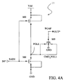
- the disturb suppression circuit 11 realised according to the invention is shown in greater detail in Figure 4A.
- the disturb suppression circuit 11 comprises an input transistor M6, in particular a MOS transistor with N channel, having a control terminal or gate connected to the input terminal IN* of the disturb suppression circuit 11, a first conduction terminal, in particular a drain terminal, connected to an inner circuit node POLE and a second conduction terminal, in particular a source terminal connected to the ground GND.
- the inner circuit node POLE is connected, by means of a switch transistor M8, in particular a MOS transistor with P channel, to the supply voltage reference Vdd.
- the disturb suppression circuit 11 also comprises a compensation capacitor inserted between the inner circuit node POLE and the output terminal OUT* of the disturb suppression circuit 11.
- this compensation capacitor is realised by means of a further coupling transistor M9, in particular a MOS transistor with N channel, having the conduction terminals connected to the inner circuit node POLE and a control terminal or gate connected to the output terminal OUT*, in turn connected to the input terminal IN of the Rand Gap circuitry 10 and receiving the Band Gap voltage BGAP.
- a threshold transistor M7 is also inserted between the switch transistor M8 and the inner circuit node POLE.
- the threshold transistor M7 has a control terminal or gate connected to the output terminal OUT*, a first conduction terminal, in particular a drain terminal, connected to the switch transistor M8 and a second conduction terminal, in particular a source terminal, connected to the inner circuit node POLE.
- the switch transistor M8 has a control terminal or gate connected to the input terminal IN*, a first conduction terminal, in particular a source terminal, connected to the supply voltage reference Vdd and a second conduction terminal, in particular a drain terminal, connected to the threshold transistor M7.
- the threshold transistor M7 is a natural transistor in cascode configuration and it has a bulk terminal connected to the ground GND, while the switch transistor M8 has a bulk terminal connected to the supply voltage reference.
- the coupling transistor M9 has a control terminal or gate connected to the output terminal OUT*, a first and a second conduction terminal connected to the inner circuit node POLE and a bulk terminal connected to the ground GND.
- the coupling transistor M9 thus serves as capacitor for compensating the variations introduced through capacitive coupling by the switch on and off of the circuits or loads connected to the Band Gap circuitry 10, in particular sense amplifiers.
- the disturb suppression circuit 11 provides that a capacitor (realised by the coupling transistor M9) is connected between the output terminal OUT*, where there is the Band Gap voltage signal BGAP, and the inner circuit node POLE, where the control signal CMD_POLE is applied so that the disturb suppression signal 11 has a behaviour opposed to the Band Gap circuitry 10 under on and off conditions of the same and thus of the load connected thereto, in particular a sense amplifier.
- the further enable signal SAEN has a low value, in particular the ground value GND, and applies, the input transistor M6 being off, a positive voltage value to the inner circuit node POLE thanks to the switch on of the switch transistor MS.
- this positive voltage value is given by the supply voltage Vdd
- this positive voltage value is given by the Band Gap voltage BGAP decreased by a threshold voltage value Vth of the threshold transistor M7.
- the enable signal SAEN_N is brought to a low value while the further enable signal SAEN is brought at a high value, in particular to the supply voltage value Vdd, switching on the input transistor M6 and forcing the inner circuit node POLE to a value corresponding to the ground GND.
- the capacitor realised by the coupling transistor M9 decreases the potential value of the output terminal OUT*, i.e. of the Rand Gap voltage signal BGAP, compensating the behaviour of the rest of the Band Gap circuitry 10 which, as previously described In connection with the prior art, tends instead to enhance this Band Gap voltage signal BGAP.
- the value of the capacitor realised by the coupling transistor M9 and the variation of the potential of the control signal CMD_POLE are suitably calibrated for compensating at the best the behaviour of the rest of the Band Gap circuitry 10 and in particular the injection of positive charge created by the switch on of the current mirror 3.
- the control signal CMD_POLE is brought to a value equal to the supply voltage Vdd.
- Vdd the supply voltage
- a little noisy supply voltage reference is to be provided, to avoid introducing, through capacitive coupling, this noise on the output terminal OUT*, i.e. on the Band Gap node.
- the control signal CMD_POLE is brought to a value equal to the Band Gap voltage BGAP decreased by a threshold voltage value of the threshold transistor M7.
- the threshold transistor M7 is a natural transistor, thus having a very little threshold voltage value, connected to the output terminal OUT* in a cascode configuration. In this way, the threshold transistor M7 allows to de-couple the supply voltage reference Vdd from the output terminal OUT*, i.e. from the Band Gap node.
- control signal CMD_POLE has however definitely low voltage values, which must be suitably managed.
- the transistor M9 which realises the coupling capacitor with the Band Gap node BGAP is a Low Voltage transistor having dimensions that can be compared with those of the LV transistor M1 of the controlled current generator 2, to obtain a better emulation of the opposite behaviour of the Band Gap circuitry 10 under on and/or off conditions.
- the method for generating a controlled current, the circuit for suppressing disturbs and the Band Gap circuitry realised according to the invention allow to compensate the disturbs introduced through capacitive coupling by the switch on/off of sense amplifiers on a sense amplifier already operating and attain several advantages among which an enormous functional and structural simplicity of the circuits proposed, which allow an easy regulation of their operation together with a containment of the costs and of the areas necessary for realising them.
- the method for generating a regulated current has a beneficial effect also on the self-induced disturbs, i.e. on the operation disturbs of a sense amplifier linked to the switch on of the other sense amplifiers belonging to a same bank.
- the disturb compensation obtained ensures the correct operation of all the sense amplifiers of a bank, independently from the switch on/off conditions of the other sense amplifiers of this bank.
Landscapes
- Engineering & Computer Science (AREA)
- Power Engineering (AREA)
- Microelectronics & Electronic Packaging (AREA)
- Physics & Mathematics (AREA)
- Nonlinear Science (AREA)
- Electromagnetism (AREA)
- General Physics & Mathematics (AREA)
- Radar, Positioning & Navigation (AREA)
- Automation & Control Theory (AREA)
- Control Of Electrical Variables (AREA)
Abstract
- supplying on a Band Gap node (BGAP), a Band Gap voltage signal that is stable in temperature and power supply;
- driving a controlled current generator (2) by means of this Band Gap voltage signal; and
mirroring the controlled current signal generated on an output terminal of the Band Gap circuitry;
Advantageously according to the invention, the method further comprises, after the driving step, a step of locally suppressing a disturb of the controlled current signal generated by the controlled current generator (2) by means of a disturb suppression circuit (11) connected to said Band Gap node acting on said Band Gap voltage signal.
A disturb suppression circuit and a Band Gap circuitry for the generation of a controlled current signal are also described.
Description
- The present Invention relates to a method for generating a controlled current by means of a Band Gap circuitry and to a relative circuit for suppressing disturbs and Band Gap circuitry for the generation of a controlled current.
- More specifically, the invention relates to a method for generating a controlled current by means of a Band Gap circuitry of the type comprising the steps of:
- supplying, on a Band Gap node, a Band Gap voltage signal that is stable in temperature and power supply;
- driving a controlled current generator by means of this Band Gap voltage signal, and
- mirroring said controlled current signal generated on an output terminal of said Band Gap circuitry.
- The invention also relates to a circuit for suppressing disturbs and to a Band Gap circuitry for the generation of a controlled current signal.
- The invention particularly, but not exclusively, relates to the generation of a controlled current signal for banks of sense amplifiers in memory devices of the Dual Work type and the following description is made with reference to this field of application in order to simplify its disclosure.
- As it is well known, memory devices of the Flash EPROM type, so called Dual Work, have the possibility of simultaneously and independently reading on two different memory partitions, a first partition under real reading condition and a second partition under verify after modification condition.
- Thus, these devices need a sense amplifier structure with high parallelism for having a high flow of output data. In particular, these sense amplifiers are organised in banks.
- It is also known that each sense amplifier uses, for its operation, a reference voltage that is stable in power supply and temperature, usually called Band Gap voltage and hereafter indicated as BGAP voltage. This BGAP voltage is usually generated by a so called Band Gap Reference Voltage Generator, normally inside the memory device.
- During the operation of the memory device, the switch on of a bank of sense amplifiers produces a transient disturb on the Band Gap voltage BGAP, which in turn affects the performances of another bank of sense amplifiers that maybe already in a on state. In general, this cross disturb phenomenon is real also in the case of single sense amplifiers.
- More in detail, inside a sense amplifier the Band Gap voltage BGAP of is generally used for generating a controlled current, i.e. a current showing a desired progress in temperature and power supply.
- To the purpose, it is known to use a transient of the MOS type with N channel, in particular of the Low Voltage type (indicated as LV transistor) degenerated in correspondence with its source terminal by a degeneration resistor. This LV transistor has a gate terminal controlled by the Band Gap voltage BGAP.
- The degeneration resistor and the LV transistor are selected so as to obtain a controlled progress of the current thus generated with respect to variations of current and power supply, this progress being established for example on the basis of the needs of the memory device design.
- The so obtained controlled current is then drawn from a current mirror, usually realised with MOS transistors with P channel and used in the sense amplifier, in any circuit node inside it where a controlled current signal is requested.
- To avoid that the sense amplifier consumes also when it is not used, due to this controlled current generator, this current mirror is also equipped with enable switches, also these latter being usually realised by means of P channel MOS transistors.
- An embodiment of the sense amplifier architecture described, i.e. of the generation circuitry, starting from a Band Gap voltage stable in temperature and power supply, of the controlled current is schematically shown in Figure 1, globally indicated with 1 and hereafter called Band Gap circuitry.
- In particular, the
Band Gap circuitry 1 essentially comprises a controlledcurrent generator 2, acurrent mirror 3 and an enablecircuitry 4, inserted, in cascade to each other, between a first and a second voltage reference, in particular a supply Vdd and a ground GND. - As above described, the controlled
current generator 2 comprises an LV transistor M1, in particular of the MOS type with N channel, having a control terminal or gate connected to an input terminal IN of theBand Gap circuitry 1, receiving the Band Gap voltage BGAP, a first conduction terminal, in particular a source terminal, connected to the ground GND through a degeneration resistor R0 and a second conduction terminal, in particular a drain terminal, connected to thecurrent mirror 3. - In turn, the
current mirror 3 comprises a first mirror transistor M2, in particular of the MOS type with P channel, being diode configured, inserted between the enablecircuitry 4 and the controlledcurrent generator 2 and having a control terminal or gate connected to a control terminal or gate of a second mirror transistor M3, inserted between the enablecircuitry 4 and an output terminal OUT of theBand Gap circuitry 1. On the output terminal OUT of theBand Gap circuitry 1 an output controlled current signal I_OUT is then generated. - Finally, the enable
circuitry 4 comprises a first enable transistor M4 inserted between the supply reference Vdd and the first mirror transistor M2 of thecurrent mirror 3 and having a control terminal or gate receiving an enable signal SAEN_N, as well as a second enable transistor M5 inserted between the supply reference Vdd and the second mirror transistor M3 of thecurrent mirror 3 and having a control terminal or gate receiving the enable signal SAEN_N. - In the embodiment shown in the Figure, the LV transistor M1 of the controlled
current generator 2 has a bulk terminal connected to the ground GND, while the mirror transistors M2 and M3 as well as the enable transistors M4 and M5 have bulk terminals connected to the supply voltage reference Vdd. - When the sense amplifier comprising the
Band Gap circuitry 1 is switched on, the enable signal SAEN_N passes from a value corresponding to the supply reference Vdd to a ground value GND. - In an initial step, the drain terminal of the LV transistor M1 of the controlled
current generator 2 is disconnected from the rest of the circuitry of the sense amplifier and the LV transistor M1 is on. Thus, the channel of this LV transistor M1 is formed and, through the degeneration resistor R0, it is at a ground potential value GND, usually 0V. - Under these conditions, also the drain terminal of the LV transistor M1 is thus at a ground potential value GND, i.e. at 0V potential.
- At the switch on of the sense amplifier, the potential values of the source terminals of the transistors M2 and M3 of the
current mirror 3 are brought to the value of the supply voltage reference Vdd and - in consequence - a current starts to flow in these transistors and the potential of the drain terminal of the LV transistor M1 enhances up to a value equal to a tripping voltage which enables thecurrent mirror 3 to operate correctly. - With the enhancement of the potential of this drain terminal of the LV transistor M1 the channel is no more uniformly biased at the ground potential value GND.
- Thus, due to its capacitive coupling to the channel and to the drain terminal, also the gate terminal of the LV transistor M1 tends to "move upwards", i.e. it tends to reach greater potential values thus creating a disturb in the Band Gap voltage value which is transferred onto the generated current value.
- All this occurs in real situations, since the Band Gap voltage BGAP is not produced, obviously, by an ideal voltage generator and thus only after a certain period of time, indicated as disturb period, tins capacitive coupling disturb between terminals of the LV transistor M1 is recovered by the generator - real - of the Band Gap voltage BGAP.
- This mechanism of generation and recovery of the capacitive coupling disturb is schematically shown in Figure 2. In particular, in this Figure the diagrams A and B show a first and a second enable signal, SA_EN Bank(1) and SA EN Bank(2), which switch on and off (in correspondence with different time instants and for a high and low value of the enable signal, respectively) a first and a second bank of sense amplifiers, for example of a memory device of the Dual Work type.
- The switch on of the banks of sense amplifiers changes the progress of the Band Gap voltage signal BGAP, as shown in the diagram C, in particular enhancing it in correspondence with the switch on of a bank of sense amplifiers and decreasing it in correspondence with its switch off, with overlapping of these enhancements and decreases in the case of different banks of sense amplifiers. As above explained, the diagram C shows how the Band Gap voltage BGAP departs from its ideal value BGAP Typical Value for the disturb period, indicated with Tr in the figure.
- During the disturb period Tr also the controlled current reference values a bank of sense amplifiers is supplied with, indicated as I_ref Bank(1) and I_ref Bank(2) thus show a progress affected by the switch on and by the switch off of another bank, as the diagrams D and E of Figure 2 show.
- In other words, the switch on/off of a bank of sense amplifiers affects the other banks of sense amplifiers in the memory device.
- It is worthwhile to note, that, since the circuit node wherein the Band Gap voltage BGAP is present is shared (indicated as BGAP node) by all the sense amplifiers of a partition (and of all the partitions) of the memory device connected to these sense amplifiers and since the number of sense amplifiers per partition is very high (normally higher than 100) it is impossible to stabilise this BGAP node by simply "reinforcing" the Band Gap voltage generator BGAP, for example with an over-dimension of its output buffer.
- It is also possible to locally interface the Band Gap voltage value BGAP for each partition of the memory device by means of a suitable analog buffer. In reality, such a solution is expensive in terms of area and/or of consumption.
- Finally, it is possible to introduce a local filtering of the Band Gap voltage value BGAP by means of suitable resistors connected between each partition and the BGAP node, which is a strongly "capacitive" node. In this case, each resistor realises, with such a BGAP node, a low-pass filter.
- In reality, by using such a local filtering, the value of the controlled current the sense amplifiers are supplied with is however locally disturbed inside the bank being switched on, the switch on occurrence however producing a much more modest effect on a possible further bank being already active. Moreover, the action of such a local filtering is slow.
- In substance, we can say that memory devices realised up to now show the common problem of the mutual influence between the banks of sense amplifiers they contain, the switch on of a bank of sense amplifiers however introducing a disturb for another bank already on, with consequent potential reading errors.
- The technical problem underlying the present invention is that of devising a method for generating a controlled current and a relative Band Gap circuitry, for example inside a sense amplifier, having such structural and functional characteristics as to allow to eliminate or in any case reduce the disturbs linked to the switch on and to the switch off of these circuitries, thus overcoming the limits and the drawbacks still affecting the devices realised according to the prior art.
- The solution idea underlying the present invention is that of locally suppressing, by means of a suitable suppression circuit, the disturbs affecting the controlled current generated starting from a Band Gap voltage and linked to the capacitive couplings inside the Rand Gap circuitry.
- On the basis of this solution idea the technical problem is solved by a method for generating a controlled current as previously indicated and defined by the characterising part of
claim 1. - The problem is also solved by a circuit for suppressing local disturbs of a Band Gap circuitry as previously indicated and defined by the characterising part of
claim 4. - Finally, the problem is solved by a Band Gap circuitry as previously indicated and defined by the characterising part of claim 20.
- The characteristics and the advantages of the method, of the circuit and of the Band Gap circuitry according to the invention will be apparent from the following description of embodiments thereof given by way of indicative and non limiting examples with reference to the annexed drawings.
- In these drawings:
- Figure 1: schematically shows a Band Gap circuitry, inside a sense amplifier and realised according to the prior art;
- Figure 2: schematically shows the progress of signals inside a first and a second bank of sense amplifiers equipped with the Band Gap circuitry of Figure 1;
- Figure 3: schematically shows a Band Gap circuitry realised according to the invention;
- Figure 4A and 4B: schematically show a circuit for suppressing disturbs inside the circuitry of Figure 3.
- The present invention arises from the consideration that, in its most general form, a disturb linked to the switch on of a sense amplifier must be locally suppressed, so as to avoid influencing the operation of a further sense amplifier already operating, for example in a memory device of the Dual Work type where these sense amplifiers are grouped in banks and can operate simultaneously.
- Advantageously according to the invention, a method is proposed for generating a controlled current by means of a Band Gap circuitry comprising the steps of
- supplying, on a Band Gap node, a voltage signal that is stable in temperature and power supply, indicated as Band Gap voltage;
- driving a controlled current generator by means of this Band Gap voltage signal;
- locally suppressing a disturb of a controlled current signal generated by the controlled current generator by means of a disturb suppression circuit connected to the Band Gap node acting un this Band Gap voltage signal; and
- mirroring the controlled current signal generated on an output terminal of the Band Gap circuitry.
- In particular, the step of locally suppressing the disturb of the controlled current signal comprises a step of emulating a behaviour that is opposite to a behaviour of a circuit or load connected to the Band Gap circuitry, in particular a sense amplifier. In substance, the method provides that this emulating step influences the controlled current generated by the Band Gap circuitry in the opposite direction with respect to the influence of the load connected thereto, cancelling the disturb effects of this load on the controlled current thus generated.
- Advantageously according to the invention, the emulating step particularly provides the use of a compensation capacitor connected to the Band Gap node and driven by an enable signal SAEN opposed to an enable signal SAEN_N of the Band Gap circuitry.
- The method for generating a controlled current according to the invention is implemented by means of a Band Gap circuitry, schematically shown in Figure 3 and globally indicated with 10.
- The
Band Gap circuitry 10 according to the invention has a base structure corresponding to theBand Gap circuitry 1 described in connection with the prior art and shown in Figure 1. Structurally and functionally identical elements will be given the same reference numbers by way of illustration. - The
Band Gap circuitry 10 thus comprises, as previously seen, a controlledcurrent generator 2, acurrent mirror 3 and an enablecircuitry 4, cascade inserted between a first and a second voltage reference, in particular a supply voltage Vdd and a ground potential GND. - The
current generator 2 comprises a LV transistor M1, in particular of the MOS type with N channel, having a control terminal or gate connected to an input terminal IN of theBand Gap circuitry 1, receiving the Band Gap voltage BGAP and corresponding to a Band Gap node BGAP, a first conduction terminal, in particular a source terminal, connected to the ground GND through a degeneration resistor RO and a second conduction terminal, in particular a drain terminal, connected to thecurrent mirror 3. - In turn, the
current mirror 3 comprises a first mirror transistor M2, in particular of the MOS type with P channel, diode configured, inserted between the enablecircuitry 4 and thegenerator 2 of a Band Gap voltage and having a control terminal or gate connected to a control terminal or gate of a second mirror transistor M3, inserted between the enablecircuitry 4 and an output terminal OUT of theBand Gap circuitry 1, where an output controlled current signal I_OUT is generated. - Finally, the enable
circuitry 4 comprises a first enable transistor M4 inserted between the supply reference Vdd and the first mirror transistor M2 of thecurrent mirror 3 and having a control terminal or gate receiving an enable signal SAEN_N, as well as a second enable transistor M5 inserted between the supply reference Vdd and the second mirror transistor M3 of thecurrent mirror 3 and having a control terminal or gate receiving the enable signal SAEN_N. - Advantageously according to the invention, the
Band Gap circuitry 10 also comprises a disturbsuppression circuit 11, having an input terminal IN* receiving a further enable signal SAEN and an output terminal OUT* connected to the input terminal IN of theBand Gap circuitry 10. In particular, the disturbsuppression circuit 11 realises the step of the local suppression of disturbs, as it will be apparent hereafter in the description. - In the embodiment shown in the Figure, the LV transistor M1 of the controlled
current generator 2 has a bulk terminal connected to the ground GND, while the mirror transistors M2 and M3 as well as the enable transistors M4 and M5 have bulk terminals connected to the supply voltage reference Vdd. - The disturb
suppression circuit 11 realised according to the invention is shown in greater detail in Figure 4A. - In particular, the disturb
suppression circuit 11 comprises an input transistor M6, in particular a MOS transistor with N channel, having a control terminal or gate connected to the input terminal IN* of the disturbsuppression circuit 11, a first conduction terminal, in particular a drain terminal, connected to an inner circuit node POLE and a second conduction terminal, in particular a source terminal connected to the ground GND. - The inner circuit node POLE is connected, by means of a switch transistor M8, in particular a MOS transistor with P channel, to the supply voltage reference Vdd.
- Advantageously according to the invention, the disturb
suppression circuit 11 also comprises a compensation capacitor inserted between the inner circuit node POLE and the output terminal OUT* of the disturbsuppression circuit 11. In the embodiment shown in Figure 4A, this compensation capacitor is realised by means of a further coupling transistor M9, in particular a MOS transistor with N channel, having the conduction terminals connected to the inner circuit node POLE and a control terminal or gate connected to the output terminal OUT*, in turn connected to the input terminal IN of theRand Gap circuitry 10 and receiving the Band Gap voltage BGAP. - In a preferred embodiment of the disturb
suppression circuit 11 according to the invention, shown in Figure 4B, a threshold transistor M7 is also inserted between the switch transistor M8 and the inner circuit node POLE. - In particular, the threshold transistor M7 has a control terminal or gate connected to the output terminal OUT*, a first conduction terminal, in particular a drain terminal, connected to the switch transistor M8 and a second conduction terminal, in particular a source terminal, connected to the inner circuit node POLE.
- Moreover, the switch transistor M8 has a control terminal or gate connected to the input terminal IN*, a first conduction terminal, in particular a source terminal, connected to the supply voltage reference Vdd and a second conduction terminal, in particular a drain terminal, connected to the threshold transistor M7.
- In the embodiment shown in Figure 4B, the threshold transistor M7 is a natural transistor in cascode configuration and it has a bulk terminal connected to the ground GND, while the switch transistor M8 has a bulk terminal connected to the supply voltage reference.
- Finally, the coupling transistor M9 has a control terminal or gate connected to the output terminal OUT*, a first and a second conduction terminal connected to the inner circuit node POLE and a bulk terminal connected to the ground GND. The coupling transistor M9 thus serves as capacitor for compensating the variations introduced through capacitive coupling by the switch on and off of the circuits or loads connected to the
Band Gap circuitry 10, in particular sense amplifiers. - It is worthwhile tonote that on the inner circuit node POLE there is a control signal CMD_POLE, that the input terminal IN* receives the further enable signal SAEN, that is the inverted enable signal SAEN_N for the enable transistors M4 and M5 of the enable
circuitry 4 and that the output terminal OUT* supplies a current signal BGAP compensated with the disturbs. - Let's now see the operation of the disturb
suppression circuit 11 according to the invention, that substantially emulates a behaviour opposite with respect to the rest of theBand Gap circuitry 10 in correspondence with the switch on of a load, in particular a sense amplifier to whom thisBand Gap circuitry 10 is connected. - Advantageously according to the invention, the disturb
suppression circuit 11 provides that a capacitor (realised by the coupling transistor M9) is connected between the output terminal OUT*, where there is the Band Gap voltage signal BGAP, and the inner circuit node POLE, where the control signal CMD_POLE is applied so that the disturbsuppression signal 11 has a behaviour opposed to theBand Gap circuitry 10 under on and off conditions of the same and thus of the load connected thereto, in particular a sense amplifier. - In particular, under off conditions of the sense amplifier, i.e. for high values of the enable signal SAEN_N of the enable
circuitry 4, the further enable signal SAEN has a low value, in particular the ground value GND, and applies, the input transistor M6 being off, a positive voltage value to the inner circuit node POLE thanks to the switch on of the switch transistor MS. In its embodiment shown in Figure 4A, this positive voltage value is given by the supply voltage Vdd, while in the embodiment shown in Figure 4B, this positive voltage value is given by the Band Gap voltage BGAP decreased by a threshold voltage value Vth of the threshold transistor M7. - At the switch on of the sense amplifier, the enable signal SAEN_N is brought to a low value while the further enable signal SAEN is brought at a high value, in particular to the supply voltage value Vdd, switching on the input transistor M6 and forcing the inner circuit node POLE to a value corresponding to the ground GND. Under these conditions, the capacitor realised by the coupling transistor M9 decreases the potential value of the output terminal OUT*, i.e. of the Rand Gap voltage signal BGAP, compensating the behaviour of the rest of the
Band Gap circuitry 10 which, as previously described In connection with the prior art, tends instead to enhance this Band Gap voltage signal BGAP. - Advantageously according to the invention, the value of the capacitor realised by the coupling transistor M9 and the variation of the potential of the control signal CMD_POLE are suitably calibrated for compensating at the best the behaviour of the rest of the
Band Gap circuitry 10 and in particular the injection of positive charge created by the switch on of thecurrent mirror 3. - In particular, when the sense amplifier is off, the control signal CMD_POLE is brought to a value equal to the supply voltage Vdd. In this case, a little noisy supply voltage reference is to be provided, to avoid introducing, through capacitive coupling, this noise on the output terminal OUT*, i.e. on the Band Gap node.
- As it has been seen in a preferred embodiment of the disturb
suppression circuit 11, if the disturbsuppression circuit 11 includes the threshold transistor M7, the control signal CMD_POLE is brought to a value equal to the Band Gap voltage BGAP decreased by a threshold voltage value of the threshold transistor M7. - In a further preferred embodiment, the threshold transistor M7 is a natural transistor, thus having a very little threshold voltage value, connected to the output terminal OUT* in a cascode configuration. In this way, the threshold transistor M7 allows to de-couple the supply voltage reference Vdd from the output terminal OUT*, i.e. from the Band Gap node.
- It is also possible to use a threshold transistor M7 realised by a Low Voltage transistor, to further improve the de-coupling between the supply voltage reference Vdd and Band Gap node. In this case, the control signal CMD_POLE has however definitely low voltage values, which must be suitably managed.
- Finally, the transistor M9 which realises the coupling capacitor with the Band Gap node BGAP is a Low Voltage transistor having dimensions that can be compared with those of the LV transistor M1 of the controlled
current generator 2, to obtain a better emulation of the opposite behaviour of theBand Gap circuitry 10 under on and/or off conditions. - It is obvious that similar considerations are also valid in case of off conditions. In particular, the following conditions are valid:
- if the sense amplifier is off (OFF), the input transistor M6 is off (OFF) and the switch transistor M8 is on (ON); while
- if the sense amplifier is on (ON), the input transistor M6 is on (ON) and the switch transistor M8 is off (OFF).
- In conclusion, the method for generating a controlled current, the circuit for suppressing disturbs and the Band Gap circuitry realised according to the invention allow to compensate the disturbs introduced through capacitive coupling by the switch on/off of sense amplifiers on a sense amplifier already operating and attain several advantages among which an incredible functional and structural simplicity of the circuits proposed, which allow an easy regulation of their operation together with a containment of the costs and of the areas necessary for realising them.
- Moreover, advantageously according to the invention, the method for generating a regulated current has a beneficial effect also on the self-induced disturbs, i.e. on the operation disturbs of a sense amplifier linked to the switch on of the other sense amplifiers belonging to a same bank. In particular, the disturb compensation obtained ensures the correct operation of all the sense amplifiers of a bank, independently from the switch on/off conditions of the other sense amplifiers of this bank.
Claims (22)
- Method for generating a controlled current by means of a Band Gap circuitry comprising the steps of:- supplying, on a Band Gap node, a Band Gap voltage signal that is stable in temperature and power supply;- driving a controlled current generator by means of said Band Gap voltage signal; and- mirroring said controlled current signal generated on an output terminal of said Band Gap circuitry;characterised in that it further comprises, after said driving step, a step of locally suppressing a disturb of a controlled current signal generated by a controlled current generator by means of a disturb suppression circuit (11) connected to said Band Gap node acting on said Band Gap voltage signal.
- Method for generating a controlled current according to claim 1, characterised in that said step of locally suppressing said disturb of said controlled current signal comprises a step of emulating a behaviour that is opposite to a behaviour of a load circuit connected to said Band Gap circuitry.
- Method for generating a controlled current according to claim 1, characterised in that said emulating step provides the use of a compensation capacitor (M9) connected to said Band Gap node and driven by an enable signal (SAEN) opposite to an enable signal (SAEN_N) of said Band Gap circuitry.
- Circuit (11) for suppressing disturbs of a controlled current signal generated by a Band Gap circuitry on a Band Gap node (BGAP) characterised in that it comprises at least one compensation capacitor (M9) inserted between said Band Gap node (BGAP) and an inner circuit node (POLE) of said disturb suppression circuit, in turn connected to a first voltage reference (GND) by means of an input transistor (M6) having a control terminal connected to an input terminal (IN*) of said disturb suppression circuit (11) and receiving an enable signal (SAEN).
- Circuit (11) for suppressing disturbs according to claim 4, characterised in that it further comprises at least one switch (M8) inserted between a second voltage reference (Vdd) and said inner circuit node (POLE).
- Circuit (11) for suppressing disturbs according to claim 5, characterised in that it further comprises at least one threshold transistor (M7) inserted between said switch (M8) and said inner circuit node (POLE) and having a control terminal connected to said Band Gap node (BGAP).
- Circuit (11) for suppressing disturbs according to claim 4, characterised in that said compensation capacitor comprises a transistor (M9) having a control terminal connected to said Band Gap node (BGAP) and conduction terminal connected to said inner circuit node (POLE).
- Circuit (11) for suppressing disturbs according to claim 7, characterised in that said transistor (M9) is a MOS transistor with N channel.
- Circuit (11) for suppressing disturbs according to claim 8, characterised in that said transistor (M9) has a bulk terminal connected to said first voltage reference (GND).
- Circuit (11) for suppressing disturbs according to claim 8, characterised in that said transistor (M9) is a Low Voltage transistor.
- Circuit (11) for suppressing disturbs according to claim 4, characterised in that said input transistor (M6) has a first conduction terminal connected to said inner circuit node (POLE) and a second conduction terminal connected to said first voltage reference (GND).
- Circuit (11) for suppressing disturbs according to claim 11, characterised in that said input transistor (M6) is a MOS transistor with N channel.
- Circuit (11) for suppressing disturbs according to claim 12, characterised in that said input transistor (M6) has a bulk terminal connected to said first voltage reference (GND).
- Circuit (11) for suppressing disturbs according to claim 5, characterised in that said switch is a transistor (M8) having a control terminal connected to said input terminal (IN*), a first conduction terminal connected to said second voltage reference (Vdd) and a second conduction terminal connected to said inner circuit node (POLE).
- Circuit (11) for suppressing disturbs according to claim 14, characterised in that said transistor (M8) is a MOS transistor with P channel.
- Circuit (11) for suppressing disturbs according to claim 15, characterised in that said transistor (M8) has a bulk terminal connected to said second voltage reference (Vdd).
- Circuit (11) for suppressing disturbs according to claim 6, characterised in that said threshold transistor (M7) is a natural transistor in cascode configuration.
- Circuit (11) for suppressing disturbs according to claim 17, characterised in that said threshold transistor (M7) has a bulk terminal connected to said first voltage reference (GND).
- Circuit (11) for suppressing disturbs according to claim 6, characterised in that said threshold transistor (M7) is a Low Voltage transistor.
- Band Gap circuitry (10) of the type comprising at least one controlled current generator (2), a current mirror (3) and an enable circuitry (4), cascade inserted between a first and a second voltage reference (Vdd, GND), said controlled current generator (2) being connected to an input terminal (IN) receiving a Band Gap voltage signal (BGAP) that is stable in temperature and power supply, said current mirror (3) being connected to an output terminal (OUT) suitable for supplying a controlled current signal (I_OUT) and said enable circuitry (4) receiving an enable signal (SAEN_N), characterised in that it further comprises a disturb suppression circuit (11) according to any claim from 4 to 19.
- Band Gap circuitry (10) according to claim 20, characterised in that said enable signal (SAEN_N) of said enable circuitry (4) is the inverted signal of said enable signal (SAEN) of said disturb suppression circuit (11).
- Band Gap circuitry (10) according to claim 20, characterised in that said transistor (M9) which realises said coupling capacitor is a Low Voltage transistor having dimensions that may be compared with those of a transistor (M1) comprised in said controlled current generator (2).
Priority Applications (3)
| Application Number | Priority Date | Filing Date | Title |
|---|---|---|---|
| EP06425124A EP1826766B1 (en) | 2006-02-28 | 2006-02-28 | Circuit and method for generating a controlled current and suppressing disturbance thereof |
| DE602006009476T DE602006009476D1 (en) | 2006-02-28 | 2006-02-28 | Apparatus and method for generating controlled current and suppressing its interference |
| US11/712,239 US20070223168A1 (en) | 2006-02-28 | 2007-02-27 | Method for locally suppressing a disturbance of a reference line |
Applications Claiming Priority (1)
| Application Number | Priority Date | Filing Date | Title |
|---|---|---|---|
| EP06425124A EP1826766B1 (en) | 2006-02-28 | 2006-02-28 | Circuit and method for generating a controlled current and suppressing disturbance thereof |
Publications (2)
| Publication Number | Publication Date |
|---|---|
| EP1826766A1 true EP1826766A1 (en) | 2007-08-29 |
| EP1826766B1 EP1826766B1 (en) | 2009-09-30 |
Family
ID=36926407
Family Applications (1)
| Application Number | Title | Priority Date | Filing Date |
|---|---|---|---|
| EP06425124A Expired - Lifetime EP1826766B1 (en) | 2006-02-28 | 2006-02-28 | Circuit and method for generating a controlled current and suppressing disturbance thereof |
Country Status (3)
| Country | Link |
|---|---|
| US (1) | US20070223168A1 (en) |
| EP (1) | EP1826766B1 (en) |
| DE (1) | DE602006009476D1 (en) |
Families Citing this family (1)
| Publication number | Priority date | Publication date | Assignee | Title |
|---|---|---|---|---|
| FR3042876B1 (en) * | 2015-10-27 | 2017-12-15 | STMicroelectronics (Alps) SAS | DETECTION OF DISTURBANCES OF A POWER SUPPLY |
Citations (2)
| Publication number | Priority date | Publication date | Assignee | Title |
|---|---|---|---|---|
| EP0891045A1 (en) * | 1997-07-11 | 1999-01-13 | Hewlett-Packard Company | A coupling charge compensation device for VLSI circuits |
| US20050117408A1 (en) * | 2003-11-30 | 2005-06-02 | Wayne Theel | Current controlled word and sense source |
Family Cites Families (7)
| Publication number | Priority date | Publication date | Assignee | Title |
|---|---|---|---|---|
| JP3626521B2 (en) * | 1994-02-28 | 2005-03-09 | 三菱電機株式会社 | Reference potential generation circuit, potential detection circuit, and semiconductor integrated circuit device |
| JP4116133B2 (en) * | 1997-07-31 | 2008-07-09 | 株式会社東芝 | Temperature-dependent constant current generating circuit and optical semiconductor device driving circuit using the same |
| US6366167B1 (en) * | 2000-02-29 | 2002-04-02 | Gain Technology Corporation | Low voltage rail-to-rail CMOS input stage |
| JP3696145B2 (en) * | 2001-10-25 | 2005-09-14 | 株式会社東芝 | Temperature dependent constant current generator |
| US6507179B1 (en) * | 2001-11-27 | 2003-01-14 | Texas Instruments Incorporated | Low voltage bandgap circuit with improved power supply ripple rejection |
| KR100594280B1 (en) * | 2004-06-23 | 2006-06-30 | 삼성전자주식회사 | Flash memory device having a bit line voltage clamp circuit for adjusting the voltage of the bit line during the program operation, and a bit line voltage control method thereof |
| US7375503B2 (en) * | 2006-01-11 | 2008-05-20 | Atmel Corporation | System for current sensing in switched DC-to-DC converters |
-
2006
- 2006-02-28 EP EP06425124A patent/EP1826766B1/en not_active Expired - Lifetime
- 2006-02-28 DE DE602006009476T patent/DE602006009476D1/en not_active Expired - Lifetime
-
2007
- 2007-02-27 US US11/712,239 patent/US20070223168A1/en not_active Abandoned
Patent Citations (2)
| Publication number | Priority date | Publication date | Assignee | Title |
|---|---|---|---|---|
| EP0891045A1 (en) * | 1997-07-11 | 1999-01-13 | Hewlett-Packard Company | A coupling charge compensation device for VLSI circuits |
| US20050117408A1 (en) * | 2003-11-30 | 2005-06-02 | Wayne Theel | Current controlled word and sense source |
Also Published As
| Publication number | Publication date |
|---|---|
| US20070223168A1 (en) | 2007-09-27 |
| EP1826766B1 (en) | 2009-09-30 |
| DE602006009476D1 (en) | 2009-11-12 |
Similar Documents
| Publication | Publication Date | Title |
|---|---|---|
| US7180370B2 (en) | CMOS amplifiers with frequency compensating capacitors | |
| KR100381832B1 (en) | Internal Voltage Generator | |
| KR20050103213A (en) | Voltage buffer for capacitive loads | |
| EP0689286B1 (en) | Low voltage, switched capacitance circuit employing switched operational amplifiers with maximized voltage swing | |
| US7403033B2 (en) | MOS linear region impedance curvature correction | |
| US20070018621A1 (en) | Area-Efficient Capacitor-Free Low-Dropout Regulator | |
| US6380799B1 (en) | Internal voltage generation circuit having stable operating characteristics at low external supply voltages | |
| KR20100097670A (en) | Current mirror device and method | |
| JP3087838B2 (en) | Constant voltage generator | |
| US7425870B2 (en) | Current mirror circuit | |
| US9514788B1 (en) | Differential amplifier circuit, voltage regulator, and semiconductor memory device including the same | |
| US7863981B2 (en) | Rail-to-rail operational amplifier | |
| JPH06236697A (en) | Analog electric current memory device | |
| JPH08195631A (en) | Sense amplifier | |
| US7750723B2 (en) | Voltage generation circuit provided in a semiconductor integrated device | |
| US5177374A (en) | Current mode gate drive for power mos transistors | |
| US7482845B2 (en) | Output buffer circuit | |
| US11658655B2 (en) | Precharge buffer stage circuit and method | |
| US7276961B2 (en) | Constant voltage outputting circuit | |
| US5140279A (en) | Slew rate enhanced linear amplifier | |
| EP1826766B1 (en) | Circuit and method for generating a controlled current and suppressing disturbance thereof | |
| JPH05191169A (en) | Amplifier circuit and dc bias signal and method of supplying analog signal | |
| US20090066372A1 (en) | High speed cmos output buffer for nonvolatile memory devices | |
| JP2007128457A (en) | Ripple filter circuit | |
| KR20240138899A (en) | Buffer Circuit having Enhanced slew rate |
Legal Events
| Date | Code | Title | Description |
|---|---|---|---|
| PUAI | Public reference made under article 153(3) epc to a published international application that has entered the european phase |
Free format text: ORIGINAL CODE: 0009012 |
|
| AK | Designated contracting states |
Kind code of ref document: A1 Designated state(s): AT BE BG CH CY CZ DE DK EE ES FI FR GB GR HU IE IS IT LI LT LU LV MC NL PL PT RO SE SI SK TR |
|
| AX | Request for extension of the european patent |
Extension state: AL BA HR MK YU |
|
| 17P | Request for examination filed |
Effective date: 20080228 |
|
| 17Q | First examination report despatched |
Effective date: 20080409 |
|
| AKX | Designation fees paid |
Designated state(s): DE FR GB IT |
|
| GRAP | Despatch of communication of intention to grant a patent |
Free format text: ORIGINAL CODE: EPIDOSNIGR1 |
|
| RTI1 | Title (correction) |
Free format text: CIRCUIT AND METHOD FOR GENERATING A CONTROLLED CURRENT AND SUPPRESSING DISTURBANCE THEREOF |
|
| GRAS | Grant fee paid |
Free format text: ORIGINAL CODE: EPIDOSNIGR3 |
|
| GRAA | (expected) grant |
Free format text: ORIGINAL CODE: 0009210 |
|
| AK | Designated contracting states |
Kind code of ref document: B1 Designated state(s): DE FR GB IT |
|
| REG | Reference to a national code |
Ref country code: GB Ref legal event code: FG4D |
|
| REF | Corresponds to: |
Ref document number: 602006009476 Country of ref document: DE Date of ref document: 20091112 Kind code of ref document: P |
|
| RAP2 | Party data changed (patent owner data changed or rights of a patent transferred) |
Owner name: STMICROELECTRONICS SRL |
|
| PLBE | No opposition filed within time limit |
Free format text: ORIGINAL CODE: 0009261 |
|
| STAA | Information on the status of an ep patent application or granted ep patent |
Free format text: STATUS: NO OPPOSITION FILED WITHIN TIME LIMIT |
|
| 26N | No opposition filed |
Effective date: 20100701 |
|
| GBPC | Gb: european patent ceased through non-payment of renewal fee |
Effective date: 20100228 |
|
| REG | Reference to a national code |
Ref country code: FR Ref legal event code: ST Effective date: 20101029 |
|
| PG25 | Lapsed in a contracting state [announced via postgrant information from national office to epo] |
Ref country code: FR Free format text: LAPSE BECAUSE OF NON-PAYMENT OF DUE FEES Effective date: 20100301 |
|
| PG25 | Lapsed in a contracting state [announced via postgrant information from national office to epo] |
Ref country code: IT Free format text: LAPSE BECAUSE OF FAILURE TO SUBMIT A TRANSLATION OF THE DESCRIPTION OR TO PAY THE FEE WITHIN THE PRESCRIBED TIME-LIMIT Effective date: 20090930 Ref country code: GB Free format text: LAPSE BECAUSE OF NON-PAYMENT OF DUE FEES Effective date: 20100228 |
|
| REG | Reference to a national code |
Ref country code: DE Ref legal event code: R082 Ref document number: 602006009476 Country of ref document: DE Representative=s name: SAMSON & PARTNER, PATENTANWAELTE, DE |
|
| REG | Reference to a national code |
Ref country code: DE Ref legal event code: R082 Ref document number: 602006009476 Country of ref document: DE Representative=s name: SAMSON & PARTNER, PATENTANWAELTE, DE Effective date: 20130513 Ref country code: DE Ref legal event code: R081 Ref document number: 602006009476 Country of ref document: DE Owner name: MICRON TECHNOLOGY, INC., US Free format text: FORMER OWNER: STMICROELECTRONICS S.R.L., AGRATE BRIANZA, IT Effective date: 20130513 Ref country code: DE Ref legal event code: R081 Ref document number: 602006009476 Country of ref document: DE Owner name: MICRON TECHNOLOGY, INC., BOISE, US Free format text: FORMER OWNER: STMICROELECTRONICS S.R.L., AGRATE BRIANZA, MAILAND/MILANO, IT Effective date: 20130513 Ref country code: DE Ref legal event code: R082 Ref document number: 602006009476 Country of ref document: DE Representative=s name: SAMSON & PARTNER PATENTANWAELTE MBB, DE Effective date: 20130513 Ref country code: DE Ref legal event code: R081 Ref document number: 602006009476 Country of ref document: DE Owner name: MICRON TECHNOLOGY, INC., BOISE, US Free format text: FORMER OWNER: STMICROELECTRONICS S.R.L., AGRATE BRIANZA, IT Effective date: 20130513 |
|
| PGFP | Annual fee paid to national office [announced via postgrant information from national office to epo] |
Ref country code: DE Payment date: 20250226 Year of fee payment: 20 |
|
| REG | Reference to a national code |
Ref country code: DE Ref legal event code: R071 Ref document number: 602006009476 Country of ref document: DE |