EP1826665A2 - Data reordering apparatus - Google Patents
Data reordering apparatus Download PDFInfo
- Publication number
- EP1826665A2 EP1826665A2 EP06116289A EP06116289A EP1826665A2 EP 1826665 A2 EP1826665 A2 EP 1826665A2 EP 06116289 A EP06116289 A EP 06116289A EP 06116289 A EP06116289 A EP 06116289A EP 1826665 A2 EP1826665 A2 EP 1826665A2
- Authority
- EP
- European Patent Office
- Prior art keywords
- order
- entries
- positions
- information
- storage
- Prior art date
- Legal status (The legal status is an assumption and is not a legal conclusion. Google has not performed a legal analysis and makes no representation as to the accuracy of the status listed.)
- Granted
Links
Images





Classifications
-
- G—PHYSICS
- G06—COMPUTING OR CALCULATING; COUNTING
- G06F—ELECTRIC DIGITAL DATA PROCESSING
- G06F9/00—Arrangements for program control, e.g. control units
- G06F9/06—Arrangements for program control, e.g. control units using stored programs, i.e. using an internal store of processing equipment to receive or retain programs
-
- G—PHYSICS
- G06—COMPUTING OR CALCULATING; COUNTING
- G06F—ELECTRIC DIGITAL DATA PROCESSING
- G06F9/00—Arrangements for program control, e.g. control units
- G06F9/06—Arrangements for program control, e.g. control units using stored programs, i.e. using an internal store of processing equipment to receive or retain programs
- G06F9/30—Arrangements for executing machine instructions, e.g. instruction decode
- G06F9/38—Concurrent instruction execution, e.g. pipeline or look ahead
- G06F9/3836—Instruction issuing, e.g. dynamic instruction scheduling or out of order instruction execution
-
- G—PHYSICS
- G06—COMPUTING OR CALCULATING; COUNTING
- G06F—ELECTRIC DIGITAL DATA PROCESSING
- G06F9/00—Arrangements for program control, e.g. control units
- G06F9/06—Arrangements for program control, e.g. control units using stored programs, i.e. using an internal store of processing equipment to receive or retain programs
- G06F9/30—Arrangements for executing machine instructions, e.g. instruction decode
- G06F9/38—Concurrent instruction execution, e.g. pipeline or look ahead
- G06F9/3802—Instruction prefetching
-
- G—PHYSICS
- G06—COMPUTING OR CALCULATING; COUNTING
- G06F—ELECTRIC DIGITAL DATA PROCESSING
- G06F9/00—Arrangements for program control, e.g. control units
- G06F9/06—Arrangements for program control, e.g. control units using stored programs, i.e. using an internal store of processing equipment to receive or retain programs
- G06F9/30—Arrangements for executing machine instructions, e.g. instruction decode
- G06F9/38—Concurrent instruction execution, e.g. pipeline or look ahead
- G06F9/3802—Instruction prefetching
- G06F9/3814—Implementation provisions of instruction buffers, e.g. prefetch buffer; banks
-
- G—PHYSICS
- G06—COMPUTING OR CALCULATING; COUNTING
- G06F—ELECTRIC DIGITAL DATA PROCESSING
- G06F9/00—Arrangements for program control, e.g. control units
- G06F9/06—Arrangements for program control, e.g. control units using stored programs, i.e. using an internal store of processing equipment to receive or retain programs
- G06F9/30—Arrangements for executing machine instructions, e.g. instruction decode
- G06F9/38—Concurrent instruction execution, e.g. pipeline or look ahead
- G06F9/3836—Instruction issuing, e.g. dynamic instruction scheduling or out of order instruction execution
- G06F9/3838—Dependency mechanisms, e.g. register scoreboarding
- G06F9/384—Register renaming
-
- G—PHYSICS
- G06—COMPUTING OR CALCULATING; COUNTING
- G06F—ELECTRIC DIGITAL DATA PROCESSING
- G06F9/00—Arrangements for program control, e.g. control units
- G06F9/06—Arrangements for program control, e.g. control units using stored programs, i.e. using an internal store of processing equipment to receive or retain programs
- G06F9/30—Arrangements for executing machine instructions, e.g. instruction decode
- G06F9/38—Concurrent instruction execution, e.g. pipeline or look ahead
- G06F9/3854—Instruction completion, e.g. retiring, committing or graduating
- G06F9/3856—Reordering of instructions, e.g. using queues or age tags
-
- G—PHYSICS
- G06—COMPUTING OR CALCULATING; COUNTING
- G06F—ELECTRIC DIGITAL DATA PROCESSING
- G06F9/00—Arrangements for program control, e.g. control units
- G06F9/06—Arrangements for program control, e.g. control units using stored programs, i.e. using an internal store of processing equipment to receive or retain programs
- G06F9/30—Arrangements for executing machine instructions, e.g. instruction decode
- G06F9/38—Concurrent instruction execution, e.g. pipeline or look ahead
- G06F9/3854—Instruction completion, e.g. retiring, committing or graduating
- G06F9/3858—Result writeback, i.e. updating the architectural state or memory
Definitions
- the present invention relates to a reordering apparatus that changes a processing order of a plurality of processing subjects, the processing subjects being instructions within an information processing device, packets within a packet transmitting and receiving device, and the like.
- a reordering control that issues instructions in the sequence that ones ready to issue come ahead, rather than in the order that they have arrived, may be performed.
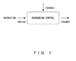
- the instructions are realigned from in the arrival order to in which the instructions marked issuable precede, as shown in Fig. 1.
- Patent Document 1 Japanese Laid-open Patent Application No. 08-110901
- Patent Document 2 Japanese Laid-open Patent Application No. 2000-048549
- Patent Document 3 Japanese Laid-open Patent Application No. 2002-304823
- An object of the present invention is to quickly and accurately retrieve a processing subject that can be processed, among a plurality of processing subj ects, such as an instruction within an information processing device, thereby reducing the time required to reorder the processing subjects.
- a reordering apparatus includes a memory device, a matrix device, a vector device, and a control device.
- the reordering apparatus holds a plurality of entries as processing subjects and changes the processing order of the entries from a first order to a second order.
- the memory device separately stores a plurality of entries waiting to be processed in different storage positions.
- the matrix device holds matrix information.
- the storage positions within the memory device correspond to row numbers and positions within the first order correspond to column numbers.
- an element corresponding to the storage position and the position within the first order of an entry stored in this storage position has a predetermined value.
- the vector device holds first vector information that indicates the storage positions of one or more processable entries, among the storage positions within the memory device.
- the control device first performs an operation between the first vector information and each column of the matrix information. Then, from the operation results of respective columns, the control device generates second vector information indicating the positions within the first order of one or more processable entries. Next, the control device selects the one to be processed from the positions within the first order of the one or more entries indicated by the second vector information and obtains the element having the predetermined value in the column corresponding to the selected position within the first order. Then, the control device processes the entry in the storage position corresponding to the obtained element, thereby actualizing the processing according to the second order.
- Fig. 2 is a principle diagram of a reordering apparatus according to the present invention.
- the reordering apparatus in Fig. 2 includes a memory device 101, a matrix device 102, a vector device 103, and a control device 104.
- the reordering apparatus holds a plurality of entries as processing subjects and changes the processing order of the entries from a first order to a second order.
- the memory device 101 separately stores the plurality of entries waiting to be processed in different storage positions.
- the matrix device 102 holds matrix information.
- the storage positions within the memory device 101 correspond to row numbers and the positions within the first order correspond to column numbers. Furthermore, in the matrix information, every element corresponding to the storage position and the position within the first order of each entry stored in this storage position has a predetermined value.
- the vector device 103 holds first vector information that indicates the storage positions of one or more processable entries, among the storage positions within the memory device 101.
- the control device 104 first performs an operation between the first vector information and each column of the matrix information. Then, from the operation results of respective columns, the control device 104 generates second vector information indicating the positions within the first order of one or more processable entries. Next, the control device 104 selects the one to be processed from the positions within the first order of the one or more entries indicated by the second vector information and obtains the element having the predetermined value in the column corresponding to the selected position within the first order. Then, the control device 104 processes the entry in the storage position corresponding to the obtained element, thereby actualizing the processing according to the second order.
- the operation between the first vector information and each column of the matrix information is performed in parallel between each element of the first vector information and all elements of each column, and the operation results of respective columns are integrated into the second vector information.
- the second vector information includes a plurality of elements indicating the positions within the first order of the processable entries
- one of the plurality of positions within the first order indicated by the elements is selected according to a predetermined policy, and the element having the predetermined value is obtained from the column in the matrix information corresponding to the selected position within the first order.
- the storage position corresponding to the element having the predetermined value is obtained, and the entry stored in the obtained storage position within the memory device 101 is processed.
- the memory device 101 corresponds, for example, to a memory region 201 in Fig. 3, described hereafter.
- the matrix information in the matrix device 102 corresponds, for example, to a bit matrix 203.
- the first vector information of the vector device 103 corresponds, for example, to a bit vector 205 in Fig. 5, described hereafter.
- the control device 104 corresponds, for example, to a reordering circuit in Fig. 11A and Fig. 11B or processing elements 1301-1 to 1301-n in Fig. 13, described hereafter.
- the position within the order of the entry that can be processed can be retrieved easily and quickly, simply by the operation between the vector information indicating the storage positions of the processable entries and each column of the matrix information. Therefore, time required to reorder the plurality of processing subjects is reduced.
- a reordering control that registers instructions in a memory region having eight storage positions and sequentially issues instructions from the instructions that can be issued, is explained with reference to Fig. 3 to Fig. 9.
- positions within an arrival order from 1 to 8, are assigned to respective storage positions, and positions within the order change every time an instruction is issued. Therefore, a bit matrix with eight rows and eight columns is used.
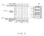
- Fig. 3 shows the bit matrix 203 when four instructions are stored in the storage region 201, such as that above.
- the row numbers 1 to 8 in the bit matrix 203 respectively correspond to the storage positions #1 to #8 in the storage region 201.
- the column numbers 1 to 8 respectively correspond to the arrival orders 1 to 8 of the instructions.
- bit strings of each column a logic "1" bit indicates the storage position of an instruction waiting to be issued (registered instruction) or the storage position waiting to store an instruction.
- Logic "0" bits indicate the other storage positions.
- columns of the arrival orders 1 to 4 hold four bit strings that respectively indicate the storage positions #6, #3, #5, and #1 of the instructions waiting to be issued.
- Columns of the arrival orders 5 to 8 hold four bit strings that respectively indicate the storage positions #8, #7, #4, and #2 waiting to store instructions.
- a bit vector 202 of the next storage position corresponds to the pointer described in (8), above.
- a logic "1" bit in the bit vector 202 indicates a column in the bit matrix 203 that holds the bit string indicating the storage position of the next instruction to arrive.
- the storage position #8 indicated by the bit string held in the column of arrival order 5 becomes the next storage position.
- a bit vector 204 for arrival order retrieval expresses the retrieval results of the instructions that can be issued.
- a logic "1" bit in the bit vector 204 indicates a column in the bit matrix 203 that holds the bit string indicating the storage position of the instruction that can be issued. In this example, no instructions that can be issued as of yet, and thus, all bits in the bit vector 204 are logic "0".
- logic "1" is included only in the AND operation result in the row of the storage position #8.
- the AND results in the rows of the other storage positions are all logic "0".
- the storage position #8 is acquired as the retrieval result in this way, and thus, the arrived instruction is stored in the storage position #8 of the memory region 201, as shown in Fig. 4.
- the pointer of the bit vector 202 (logic "1" bit) shifts one bit to the right (direction towards later arrival orders), and the bit of the arrival order 6 becomes logic "1".
- the arrival order of the instruction is retrieved. For example, if the instructions in the storage positions #1 and #3 are in an issuable state, a bit vector 205, in which the storage positions of the instructions that can be issued are logic "1", is generated, as shown in Fig. 5, and the AND operation of the bit vector 205 and the bit string in each column of the bit matrix 203 is performed. Then, in the bit matrix indicating the AND operation result of each column, logical sum (OR) is calculated for each column and the results are stored in the bit vector 204.
- the AND operation is performed in parallel between all elements in the bit vector 205 and all elements in the bit string of each column. Therefore, the instructions that can be issued can be retrieved quickly.
- the AND operation results include logic "1", and therefore, the OR operation results are logic "1".
- the arrival orders 2 and 4 are acquired as the retrieval results of the instructions that can be issued.
- the storage position of the instruction to be issued is not specified at this stage.
- the storage position of the instruction of the arrival order 2 is retrieved.
- the arrival order 4 in the bit vector 204 is changed to logic "0" and an AND operation of the bit vector 204, in which only the arrival order 2 is logic "1", and the bit string in each row of the bit matrix 203 is performed.
- logic "1" is included only in the AND operation result of the row of the storage position #3.
- the AND results of the rows of the other storage positions are all logic "0".
- the storage position #3 is acquired as the retrieval result in this way, and thus, the instruction stored in the storage position #3 of the memory region 201 is issued.
- the columns of the arrival orders 2 to 8 are rotated and shifted so that the column of the arrival order 2 in the bit matrix 203 is placed last in order, as shown in Fig. 7, and the instruction in the storage position #3 is deleted. Then, the pointer of the bit vector 202 is shifted one bit to the left, as shown in Fig. 8, to advance the arrival order of the next storage position.
- initial values of the bit matrix 203 values such as those shown in Fig. 9 are used.
- the initial values of the bit vector 202 indicate the arrival order 1, and the instructions will be stored in the storage positions #1 to #8, in the order of arrival.
- the initial values of the bit matrix 203 are selected so that the bit position of logic "1" does not overlap between rows and between columns and are not necessarily limited to the values in Fig. 9.
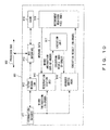
- FIG. 10 shows a configuration example of a microprocessor that executes an instruction by an out-of-order method.
- a microprocessor 901 includes an instruction decoder 911, a fetch mechanism 912, a bus interface 913, a cache 914, a reservation station (RS) 915, a reorder buffer (ROB) 916, an execution unit 917, and a retirement register file (RRF) 918.
- RS reservation station
- ROB reorder buffer
- RRF retirement register file
- the bus interface 913 accesses an external memory (not shown) via a processor bus 902.
- the fetch mechanism 912 pre-fetches a macro instruction from the memory or the cache 914.
- the instruction decoder 911 converts the macro instruction to a micro instruction string.
- the operands of the micro instruction are replaced with entries in the retirement register file 918 in preparation for out-of-order execution, and register renaming is performed.
- register renaming is performed so that an instruction, of which an operand is an execution result of a previous instruction, uses an entry as the operand, which is reserved as an execution result storage destination when the previous instruction is decoded.
- An instruction issued from the instruction decoder 911 is temporarily inputted into the reservation station 915 and waits for operand data to which there is dependency.
- a scheduler in the reservation station 915 includes a reordering circuit and sequentially issues instructions from an oldest issued instruction, among the instructions of which the operand data is completely received. At this time, the reordering circuit changes the order of the micro instructions from the order of arrival (in-order) to the order in which the instructions can be issued (out-of-order).
- the execution result of the micro instruction issued in-order (program order) from the instruction decoder 911 is required to be reflected in-order in the retirement register file 918.
- the out-of-order execution result outputted from the execution unit 917 is converted into in-order by the reorder buffer 916.
- the entry of the reordering buffer 916 is reserved as the execution result storage destination.
- Fig. 11A and Fig. 11B show configuration examples of the reordering circuit provided within the reservation station 915.
- the reordering circuit includes a release position indicator 1001, OR circuits 1002-2 to 1002-n and 1104-1 to 1104-n, AND circuits 1003-1 to 1003-n and 1103-1 to 1103-n, latch circuits 1004-1 to 1004-n (C1 to Cn), multiplexers 1005, 1006, and 1102, an allocation position indicator 1007, a release request vector 1101, inverters 1105-2 to 1105-n, and NOR circuits 1106-2 to 1106-n.
- Latch circuits 1004-1 to 1004-n always hold only one bit of logic "1" in respective different positions, and function as selectors that respectively indicate one of n entry storage positions in the memory region (not shown).
- the release position indicator 1001 corresponds to the bit vector 204 in Fig. 6 and holds a bit vector of n bits indicating a position within an order of an entry (micro instruction) to be issued (released) next. However, if there is no entry to be released, all bits are logic "0".
- the OR circuit 1002-2 outputs the logical sum of the first and second bits of the release position indicator 1001.
- the AND circuit 1003-1 outputs the logical product of a release indicating pulse P1 and the first bit of the release position indicator 1001 to the latch circuit 1004-1.
- the AND circuit 1003-1 to 1003-(k-1) outputs logic "0”
- the AND circuit 1003-k to 1003-n outputs logic "1" (latch indicating signal).
- the latch circuit 1004-n outputs a bit string of n bits, and latches the bit string outputted from the multiplexer 1005 when the AND circuit 1003-n outputs the latch indicating signal.
- the multiplexer 1005 selects the k-th bit string indicated by the release position indicator 1001, among the n number of bit strings outputted from the latch circuits 1004-1 to 1004-n, and outputs the selected bit string to the latch circuit 1004-n.
- the latch circuits 1004-k to 1004-n perform the rotation and shift operation shown in Fig. 7, by the latch indicating signal generated from the release indicating pulse P1 and bit vector of the release position indicator 1001. At this time, the latch circuits 1004-1 to 1004-n constantly maintain an allocation order (arrival order).
- the allocation position indicator 1007 corresponds to the bit vector 202 in Fig. 3.
- the allocation position indicator 1007 holds n+1 bits, that is the total of a bit vector of n bits indicating the position within the order of the next entry to arrive and a save bit (1 bit) at the time of full-entry, and always holds only one bit of logic "1".
- the bit vector indicates any one of the latch circuits 1004-1 to 1004-n.
- the allocation position indicator 1007 monitors the number of entry-registered storage positions by the position of the bit having the value of logic "1" within the bit vector and the save bit, and outputs a full-entry signal S2 as logic "1" when entries are stored in all storage positions.
- the allocation position indicator 1007 shifts the bit vector to the direction in which entries decrease (left direction) when the release indicating pulse P1 is inputted, and shifts the bit vector to the direction in which the entries increase (right direction) when the allocation indicating pulse P2 is inputted. However, the shift operation is not performed when both pulses are inputted simultaneously.
- the multiplexer 1006 selects the bit string indicated by the allocation position indicator 1007, among the n number of bit strings outputted from the latch circuit 1004-1 to 1004-n, and outputs the selected bit string as a storage allocating pointer S1. As a result, the next entry to arrive is stored in the storage position indicated by the storage allocating pointer S1.
- the release request vector 1101 corresponds to the bit vector 205 in Fig. 5 and holds a bit vector of n bits. Each bit indicates a release request of each entry, and a bit corresponding to an entry requested to release holds the value of logic "1". Therefore, when the release of a plurality of entries is requested, a plurality of bits are logic "1".
- the latch circuits 1004-1 to 1004-n constantly maintain the allocation order. Therefore, by a comparison of the release request vector 1101 and these bit strings, information in the release request vector 1101 can be reordered in the order of allocation, and a position within the order of the oldest entry can be extracted. This operation is performed as follows:
- the OR circuit 1104-1 outputs the logical sum (OR reduction) of n bits outputted from the AND circuit 1103-1.
- the NOR circuit 1106-i outputs the inversion of the logical sum of the output of the inverter 1105-i and the output of the OR circuit 1104-(i-1).
- the release position indicator 1001 holds the output of the OR circuit 1104-1 as the first bit and the outputs of the NOR circuits 1106-2 to 1106-n as the second to n-th bits.
- the OR circuit 1104-k outputs logic "1" and all NOR circuits 1106-(k+1) to 1106-n output logic "0".
- the release position indicator 1001 holds the bit vector, in which only the bit corresponding to the left-most position within the order is logic "1", among the positions within the order of the plurality of entries of which release is requested, and the other bits are logic "0".
- This bit vector indicates the position within the order of the oldest entry among the plurality of entries of which release is requested.
- the multiplexer 1102 selects the bit string indicated by the release position indicator 1001, among the n number of bit strings outputted from the latch circuits 1004-1 to 1004-n and outputs the selected bit string as a release entry pointer S3. As a result, the entry of the storage position indicated by the release entry pointer S3 is issued (released).
- the circuit in Fig. 11B is provided to acquire the release entry pointer S3 from the release request vector 1101.
- the circuit can generally be used as a circuit for reordering to the allocation order, such as an operation to reorder matching results of allocation information and entry information in the allocation order.
- the oldest issuable instruction can be accessed without counting a retaining time of each entry. Therefore, instructions can be executed in the out-of-order method more easily and more quickly.
- the reordering control in the present invention can be applied, not only to instruction processing within a CPU, but also to various processing subjects. For example, when the processing subject is packet information within a packet transmission and reception device, a processing order of a plurality of packet information can be changed.
- Fig. 12 shows a configuration example of a network communication large scale integration (LSI) used in a packet transmission and reception device such as the above.
- a communication LSI 1201 includes a bus interface 1211, a transmission buffer 1212, a transmission management unit 1213, and a transmission interface 1214.
- an upper level program When transmitting a packet, an upper level program transfers a packet transmission request to the communication LSI 1201 via an intra-device bus 1202. Upon receiving the request, the bus interface 1211 transfers a packet length and a packet destination to the transmission management unit 1213 and requests allocation of the transmission buffer 1212.
- the transmission management unit 1213 internally generates a packet control information entry, transfers an allocation address of the transmission buffer 1212 and a number of the generated entry to the bus interface 1211, and performs allocation notification. Upon receiving the notification, the bus interface 1211 starts to write packet data into the transmission buffer 1212.
- the bus interface 1211 transfers a number of the allocated entry that can be transmitted and performs transmission-possible notification to the transmission management unit 1213.
- the transmission management unit 1213 transmits a transmission start address and a transmission packet length to the transmission interface 1214 and performs a transmission request. Upon receiving the request, the transmission interface 1214 reads the packet data from the transmission buffer 1212 and transmits the read data to the destination via an outside-of-device network 1203. After a transmission completion notification is received from the transmission interface 1214, the transmission management unit 1213 deletes the corresponding entry.
- the bus interface 1211 performs a direct memory access (DMA) transfer for writing data of these packets in parallel, and therefore, the transmission management unit 1213 is required to simultaneously maintain a plurality of entries.
- DMA direct memory access
- a packet that has been allocated later is required to be transmitted when the packet becomes transmittable, and the entries are required to be released in an order differing from the allocation order, among packets with differing destinations.
- the reordering circuit shown in Fig. 11A and Fig. 11B is provided within the transmission management unit 1213, and reordering control of the packets is performed.
- packet control information is stored in the memory region as an entry and the transmission completion notification from the transmission interface 1214 is reflected in the bit value of the release request vector 1101.
- the entry of the next packet to be transmitted is retrieved successively, or a hardware implementation using a large-scale queue circuit with a forwarding function is required.
- retrieval can be performed quickly with a small-scale circuit, and therefore, a large number of short packets can be reordered and transmitted.
- the reordering is performed with the transmission packet information as the processing subject.
- reordering can be performed similarly with reception packet information as the processing subject.
- the reordering control of the present invention can be implemented, not only by a hardware circuit, but also by software performing parallel processing.
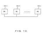
- a parallel computer such as that shown in Fig. 13, a parallel processing of a bit matrix can be performed by n number of processing elements (PE) 1301-1 to 1301-n.
- PE processing elements
Landscapes
- Engineering & Computer Science (AREA)
- Software Systems (AREA)
- Theoretical Computer Science (AREA)
- Physics & Mathematics (AREA)
- General Engineering & Computer Science (AREA)
- General Physics & Mathematics (AREA)
- Advance Control (AREA)
- Complex Calculations (AREA)
Abstract
Description
- The present invention relates to a reordering apparatus that changes a processing order of a plurality of processing subjects, the processing subjects being instructions within an information processing device, packets within a packet transmitting and receiving device, and the like.
- In an instruction handling process performed by an information processing device, a reordering control that issues instructions in the sequence that ones ready to issue come ahead, rather than in the order that they have arrived, may be performed. In this case, the instructions are realigned from in the arrival order to in which the instructions marked issuable precede, as shown in Fig. 1.
- In this way, a plural number of instructions should be maintained simultaneously, but when it issues an instruction that is issuable while others arrived earlier are not, the average latency from the arrival to the issuance should be reduced, thereby to shorten the overall execution time.
- The reordering controls like above, are conventionally implemented in microprocessors, magnetic disk devices, tape devices, and so on to optimize instruction processing (for example, refer to
Patent Documents 1 to 3, below). - Patent Document 1:
Japanese Laid-open Patent Application No. 08-110901 - Patent Document 2:
Japanese Laid-open Patent Application No. 2000-048549 - Patent Document 3:
Japanese Laid-open Patent Application No. 2002-304823 - However, in a conventional reordering control, a complicated operation is required to retrieve instructions, searching which one can be issued while they keep aligned in the arrival order, and a certain amount of processing time is also required. However, a quick and accurate decision is desired concerning which instruction to issue when plural instructions are ready, to further shorten instruction execution time.
- An object of the present invention is to quickly and accurately retrieve a processing subject that can be processed, among a plurality of processing subj ects, such as an instruction within an information processing device, thereby reducing the time required to reorder the processing subjects.
- According to the present invention, a reordering apparatus includes a memory device, a matrix device, a vector device, and a control device. The reordering apparatus holds a plurality of entries as processing subjects and changes the processing order of the entries from a first order to a second order.
- The memory device separately stores a plurality of entries waiting to be processed in different storage positions. The matrix device holds matrix information. In the matrix information, the storage positions within the memory device correspond to row numbers and positions within the first order correspond to column numbers. Furthermore, in the matrix information, an element corresponding to the storage position and the position within the first order of an entry stored in this storage position has a predetermined value. The vector device holds first vector information that indicates the storage positions of one or more processable entries, among the storage positions within the memory device.
- The control device first performs an operation between the first vector information and each column of the matrix information. Then, from the operation results of respective columns, the control device generates second vector information indicating the positions within the first order of one or more processable entries. Next, the control device selects the one to be processed from the positions within the first order of the one or more entries indicated by the second vector information and obtains the element having the predetermined value in the column corresponding to the selected position within the first order. Then, the control device processes the entry in the storage position corresponding to the obtained element, thereby actualizing the processing according to the second order.
-
- Fig. 1 is a diagram showing a conventional reordering control operation;
- Fig. 2 is a principle diagram of a reordering apparatus according to the present invention;
- Fig. 3 is a diagram showing a first bit matrix;
- Fig. 4 is a diagram showing a second bit matrix;
- Fig. 5 is a diagram showing a third bit matrix;
- Fig. 6 is a diagram showing a fourth bit matrix;
- Fig. 7 is a diagram showing a fifth bit matrix;
- Fig. 8 is a diagram showing a sixth bit matrix;
- Fig. 9 is a diagram showing initial values of the bit matrix;
- Fig. 10 is a block diagram of a microprocessor;
- Fig. 11A is a block diagram (1) of a reordering circuit;
- Fig. 11B is a block diagram (2) of the reordering circuit;
- Fig. 12 is a block diagram of a communication LSI; and
- Fig. 13 is a block diagram of a parallel computer.
- Hereinafter, preferred embodiments of the present invention are described in detail, with reference to the accompanying drawings.
- Fig. 2 is a principle diagram of a reordering apparatus according to the present invention. The reordering apparatus in Fig. 2 includes a
memory device 101, amatrix device 102, avector device 103, and acontrol device 104. The reordering apparatus holds a plurality of entries as processing subjects and changes the processing order of the entries from a first order to a second order. - The
memory device 101 separately stores the plurality of entries waiting to be processed in different storage positions. Thematrix device 102 holds matrix information. In the matrix information, the storage positions within thememory device 101 correspond to row numbers and the positions within the first order correspond to column numbers. Furthermore, in the matrix information, every element corresponding to the storage position and the position within the first order of each entry stored in this storage position has a predetermined value. Thevector device 103 holds first vector information that indicates the storage positions of one or more processable entries, among the storage positions within thememory device 101. - The
control device 104 first performs an operation between the first vector information and each column of the matrix information. Then, from the operation results of respective columns, thecontrol device 104 generates second vector information indicating the positions within the first order of one or more processable entries. Next, thecontrol device 104 selects the one to be processed from the positions within the first order of the one or more entries indicated by the second vector information and obtains the element having the predetermined value in the column corresponding to the selected position within the first order. Then, thecontrol device 104 processes the entry in the storage position corresponding to the obtained element, thereby actualizing the processing according to the second order. - The operation between the first vector information and each column of the matrix information is performed in parallel between each element of the first vector information and all elements of each column, and the operation results of respective columns are integrated into the second vector information.
- If the second vector information includes a plurality of elements indicating the positions within the first order of the processable entries, one of the plurality of positions within the first order indicated by the elements is selected according to a predetermined policy, and the element having the predetermined value is obtained from the column in the matrix information corresponding to the selected position within the first order. Then, the storage position corresponding to the element having the predetermined value is obtained, and the entry stored in the obtained storage position within the
memory device 101 is processed. - The
memory device 101 corresponds, for example, to amemory region 201 in Fig. 3, described hereafter. The matrix information in thematrix device 102 corresponds, for example, to abit matrix 203. The first vector information of thevector device 103 corresponds, for example, to abit vector 205 in Fig. 5, described hereafter. Thecontrol device 104 corresponds, for example, to a reordering circuit in Fig. 11A and Fig. 11B or processing elements 1301-1 to 1301-n in Fig. 13, described hereafter. - According to the present invention, the position within the order of the entry that can be processed can be retrieved easily and quickly, simply by the operation between the vector information indicating the storage positions of the processable entries and each column of the matrix information. Therefore, time required to reorder the plurality of processing subjects is reduced.
- In the reordering control operation in the present embodiment, an instruction that can be issued is retrieved quickly and accurately through the use of a bit matrix. A summary of the reordering control operation is as follows:
- (1) A memory device that holds a bit matrix is provided. In the bit matrix, numbers correspond to a plurality of storage positions (addresses) in a memory region storing the instructions are row numbers, and numbers indicating the order in which the instructions arrived are column numbers.
In addition, all instructions waiting to be issued are stored separately in different storage positions within the memory region. Bit strings indicating the respective storage positions of the instructions are placed in the order in which the instructions arrive and stored in the plurality of columns of the bit matrix. In each bit string, logic "1" or "0" is stored in the bit corresponding to the storage position storing the instruction of the order, as a predetermined value. The other logic ("0" or "1") is stored in the bits corresponding to the other storage positions.
Furthermore, bit strings indicating the respective storage positions waiting to store instructions are aligned in an arbitrary order following the bit strings above, and also stored in the remaining plurality of columns of the bit matrix. In each bit string, logic "1" or "0" is stored in the bit corresponding to the storage position waiting to store an instruction, as a predetermined value. The other logic ("0" or "1") is stored in the bits corresponding to the other storage positions. As a result, a plurality of bit strings equivalent to all storage positions within the memory region is placed in order and held in the bit matrix. - (2) The position within the order of arrival of a certain instruction among all instructions waiting to be issued corresponds to the column number of the bit string indicating the storage position of this instruction, in the bit matrix. The positions within the order of all instructions that can be issued, among the instructions waiting to be issued, are determined using the bit matrix. Then, the position within the order of the instruction with the earliest arrival order, among the instructions that can be issued, is acquired.
- (3) In the bit matrix, the storage position indicated by the bit string in the position within the order acquired in (2), above, is acquired. The storage position corresponds to the storage position of the instruction with the earliest arrival order, among all instructions that can be issued.
- (4) The instruction in the storage position acquired in (3), above, is issued. Then, the bit string indicating the storage position of the issued instruction and all bit strings subsequent to the column number of that bit string are rotated and shifted so that the bit string indicating the storage position of the issued instruction comes last.
- (5) After the operation in (4), above, the plurality of bit strings indicating the storage positions of the remaining instructions waiting to be issued are aligned in the order of arrival in successive positions within the order from the head column of the bit matrix. The plurality of bit strings indicating all storage positions waiting to store instructions are aligned in the positions within the order following these bit strings. Therefore, the state in (1), above, is maintained.
- (6) A newly arrived instruction is stored in the storage position indicated by the bit string of the earliest order, among the plurality of bit strings indicating the storage positions waiting to store instructions in the bit matrix. As a result, the successive positions within the order in (5), above, is maintained and the state in (1), above, is maintained.
- (7) To quickly perform the operation in (2), above, an expression in which a plurality of storage positions can be overlapped, such as a bit map of the storage position, is implemented as an expression of "the bit strings indicating the storage positions".
- (8) To quickly perform the operation in (6), a pointer indicating the position within the order of the bit string of the earliest order, among the plurality of bit strings indicating the storage positions waiting to store instructions within the bit matrix, is held. When one instruction is stored in the memory region, the pointer indicates the next position within the order, and when one instruction is issued from the memory region, the pointer indicates the previous position within the order. In this way, the value of the pointer is increased and decreased. The next instruction to arrive is stored in the storage position indicated by the bit string in the position within the order indicated by the pointer, every time the pointer increases or decreases.
- Next, an example of a reordering control, that registers instructions in a memory region having eight storage positions and sequentially issues instructions from the instructions that can be issued, is explained with reference to Fig. 3 to Fig. 9. In this case, positions within an arrival order, from 1 to 8, are assigned to respective storage positions, and positions within the order change every time an instruction is issued. Therefore, a bit matrix with eight rows and eight columns is used.
- Fig. 3 shows the
bit matrix 203 when four instructions are stored in thestorage region 201, such as that above. Therow numbers 1 to 8 in thebit matrix 203 respectively correspond to thestorage positions # 1 to #8 in thestorage region 201. Thecolumn numbers 1 to 8 respectively correspond to thearrival orders 1 to 8 of the instructions. - In the bit strings of each column, a logic "1" bit indicates the storage position of an instruction waiting to be issued (registered instruction) or the storage position waiting to store an instruction. Logic "0" bits indicate the other storage positions. In this example, columns of the
arrival orders 1 to 4 hold four bit strings that respectively indicate thestorage positions # 6, #3, #5, and #1 of the instructions waiting to be issued. Columns of thearrival orders 5 to 8 hold four bit strings that respectively indicate thestorage positions # 8, #7, #4, and #2 waiting to store instructions. - A
bit vector 202 of the next storage position corresponds to the pointer described in (8), above. A logic "1" bit in thebit vector 202 indicates a column in thebit matrix 203 that holds the bit string indicating the storage position of the next instruction to arrive. In this example, thestorage position # 8 indicated by the bit string held in the column ofarrival order 5 becomes the next storage position. - A
bit vector 204 for arrival order retrieval expresses the retrieval results of the instructions that can be issued. A logic "1" bit in thebit vector 204 indicates a column in thebit matrix 203 that holds the bit string indicating the storage position of the instruction that can be issued. In this example, no instructions that can be issued as of yet, and thus, all bits in thebit vector 204 are logic "0". - When a new instruction arrives while in this state, the column of
arrival order 5 indicated by the logic "1" bit in thebit vector 202 is retrieved, and thestorage position # 8 corresponding to the logic "1" bit is acquired as the next storage position. At this time, logical product (AND) of thebit vector 202 and the bit string in each row of thebit matrix 203 is calculated. - In this case, logic "1" is included only in the AND operation result in the row of the
storage position # 8. The AND results in the rows of the other storage positions are all logic "0". Thestorage position # 8 is acquired as the retrieval result in this way, and thus, the arrived instruction is stored in thestorage position # 8 of thememory region 201, as shown in Fig. 4. At this time, the pointer of the bit vector 202 (logic "1" bit) shifts one bit to the right (direction towards later arrival orders), and the bit of thearrival order 6 becomes logic "1". - Next, when an instruction that can be issued is present within the instructions stored in the
memory region 201, the arrival order of the instruction is retrieved. For example, if the instructions in thestorage positions # 1 and #3 are in an issuable state, abit vector 205, in which the storage positions of the instructions that can be issued are logic "1", is generated, as shown in Fig. 5, and the AND operation of thebit vector 205 and the bit string in each column of thebit matrix 203 is performed. Then, in the bit matrix indicating the AND operation result of each column, logical sum (OR) is calculated for each column and the results are stored in thebit vector 204. - At this time, the AND operation is performed in parallel between all elements in the
bit vector 205 and all elements in the bit string of each column. Therefore, the instructions that can be issued can be retrieved quickly. - In this case, in the columns of
arrival orders arrival orders - Next, because the
order 2 is the earlier order among the two acquired arrival orders, the storage position of the instruction of thearrival order 2 is retrieved. At this time, as shown in Fig. 6, thearrival order 4 in thebit vector 204 is changed to logic "0" and an AND operation of thebit vector 204, in which only thearrival order 2 is logic "1", and the bit string in each row of thebit matrix 203 is performed. - In this case, logic "1" is included only in the AND operation result of the row of the
storage position # 3. The AND results of the rows of the other storage positions are all logic "0". Thestorage position # 3 is acquired as the retrieval result in this way, and thus, the instruction stored in thestorage position # 3 of thememory region 201 is issued. - When the instruction is issued, the columns of the
arrival orders 2 to 8 are rotated and shifted so that the column of thearrival order 2 in thebit matrix 203 is placed last in order, as shown in Fig. 7, and the instruction in thestorage position # 3 is deleted. Then, the pointer of thebit vector 202 is shifted one bit to the left, as shown in Fig. 8, to advance the arrival order of the next storage position. - As initial values of the
bit matrix 203, values such as those shown in Fig. 9 are used. At this time, the initial values of thebit vector 202 indicate thearrival order 1, and the instructions will be stored in thestorage positions # 1 to #8, in the order of arrival. The initial values of thebit matrix 203 are selected so that the bit position of logic "1" does not overlap between rows and between columns and are not necessarily limited to the values in Fig. 9. - According to the reordering control using a bit matrix such as the above, the following effects can be achieved:
- (a) The arrival order of the instruction that can be issued can be retrieved quickly and accurately, simply by the performance of the AND operation between the bit vector, in which the storage position of the instruction that can be issued is logic "1", and the bit string of each column of the bit matrix. In the example described above, the instruction of the arrival order, corresponding to the column in which logic "1" is included in the AND operation result, can be issued.
- (b) Even when a plurality of instructions can be issued, the same operation as that in (a), above, can be applied, simply by the generation of a similar bit vector, in which the storage positions of the instructions that can be issued are logic "1".
- (c) When retrieving the instruction to be issued, the storage position of the instruction to be issued can be easily retrieved, simply by the performance of the AND operation between the bit vector, in which the arrival order of the instruction to be issued is logic "1", and the bit string in each row of the bit matrix.
- (d) Even when a plurality of instructions can be issued, the same operation as that in (c), above, can be applied, simply by the selection of the instruction to be issued according to the arrival order.
- (e) The next instruction to be issued can be decided without performing complicated operations, such as realigning the instructions within the memory region, by the performance of rotation and shift of the columns in the bit matrix so that the column of the arrival order of the issued instruction is placed in the last arrival order of the bit matrix.
- (f) If the bit vector, in which the arrival order of the column indicating the storage position of the next instruction to arrive is logic "1", is held, the storage position to which the instruction is stored can be easily retrieved, simply by the performance of the AND operation between the bit vector and the bit string of each row of the bit matrix.
- (g) In the bit vector in (f), above, the indicating storage position can be changed simply by the performance of a shift operation in the direction towards the later arrival orders when the instruction arrives and a shift operation in the direction towards the earlier arrival orders when the instruction is issued. The shift operation of the bit vector is performed separately from the rotation and shift of the bit matrix.
- Next, a detailed example of when the foregoing reordering control is applied to an instruction processing in a central processing unit (CPU) is explained, with reference to Fig. 10 to Fig. 11B.
- Fig. 10 shows a configuration example of a microprocessor that executes an instruction by an out-of-order method. A
microprocessor 901 includes aninstruction decoder 911, a fetchmechanism 912, abus interface 913, acache 914, a reservation station (RS) 915, a reorder buffer (ROB) 916, anexecution unit 917, and a retirement register file (RRF) 918. - The
bus interface 913 accesses an external memory (not shown) via aprocessor bus 902. The fetchmechanism 912 pre-fetches a macro instruction from the memory or thecache 914. Theinstruction decoder 911 converts the macro instruction to a micro instruction string. - The operands of the micro instruction are replaced with entries in the
retirement register file 918 in preparation for out-of-order execution, and register renaming is performed. At this time, register renaming is performed so that an instruction, of which an operand is an execution result of a previous instruction, uses an entry as the operand, which is reserved as an execution result storage destination when the previous instruction is decoded. - An instruction issued from the
instruction decoder 911 is temporarily inputted into thereservation station 915 and waits for operand data to which there is dependency. A scheduler in thereservation station 915 includes a reordering circuit and sequentially issues instructions from an oldest issued instruction, among the instructions of which the operand data is completely received. At this time, the reordering circuit changes the order of the micro instructions from the order of arrival (in-order) to the order in which the instructions can be issued (out-of-order). - However, the execution result of the micro instruction issued in-order (program order) from the
instruction decoder 911 is required to be reflected in-order in theretirement register file 918. Thus, the out-of-order execution result outputted from theexecution unit 917 is converted into in-order by thereorder buffer 916. As a result, when decoding the instruction, the entry of thereordering buffer 916 is reserved as the execution result storage destination. - Fig. 11A and Fig. 11B show configuration examples of the reordering circuit provided within the
reservation station 915. The reordering circuit includes arelease position indicator 1001, OR circuits 1002-2 to 1002-n and 1104-1 to 1104-n, AND circuits 1003-1 to 1003-n and 1103-1 to 1103-n, latch circuits 1004-1 to 1004-n (C1 to Cn),multiplexers allocation position indicator 1007, arelease request vector 1101, inverters 1105-2 to 1105-n, and NOR circuits 1106-2 to 1106-n. - The latch circuits 1004-1 to 1004-n are respectively memory circuits, such as flip-flops, holding a bit string of n bits and correspond to the
bit matrix 203 in Fig. 3. In this case, a bit matrix of n rows and n columns is held in the latch circuits 1004-1 to 1004-n, and a column of an arrival order i (i=1 to n) is held in a latch circuit 1004-i. - Latch circuits 1004-1 to 1004-n always hold only one bit of logic "1" in respective different positions, and function as selectors that respectively indicate one of n entry storage positions in the memory region (not shown).
- The
release position indicator 1001 corresponds to thebit vector 204 in Fig. 6 and holds a bit vector of n bits indicating a position within an order of an entry (micro instruction) to be issued (released) next. However, if there is no entry to be released, all bits are logic "0". - The OR circuit 1002-2 outputs the logical sum of the first and second bits of the
release position indicator 1001. The OR circuit 1002-i (i=3 to n) outputs the logical sum of the output from the OR circuit 1002-(i-1) and the i-th bit of therelease position indicator 1001. - The AND circuit 1003-1 outputs the logical product of a release indicating pulse P1 and the first bit of the
release position indicator 1001 to the latch circuit 1004-1. The AND circuit 1003-i (i=2 to n) outputs the logical product of the release indicator pulse P1 and the output of the OR circuit 1002-i to the latch circuit 1004-i. - Therefore, if the release indicating pulse P1 is logic "1" when a k-th (k=1 to n) bit of the
release position indicator 1001 is logic "1", the AND circuit 1003-1 to 1003-(k-1) outputs logic "0", and the AND circuit 1003-k to 1003-n outputs logic "1" (latch indicating signal). - The latch circuit 1004-i (i=k to n-1) outputs a bit string of n bits, and latches a bit string outputted from a latch circuit 1004-(i+1) when the AND circuit 1003-i outputs the latch indicating signal. The latch circuit 1004-n outputs a bit string of n bits, and latches the bit string outputted from the
multiplexer 1005 when the AND circuit 1003-n outputs the latch indicating signal. - The
multiplexer 1005 selects the k-th bit string indicated by therelease position indicator 1001, among the n number of bit strings outputted from the latch circuits 1004-1 to 1004-n, and outputs the selected bit string to the latch circuit 1004-n. - In this way, the latch circuits 1004-k to 1004-n perform the rotation and shift operation shown in Fig. 7, by the latch indicating signal generated from the release indicating pulse P1 and bit vector of the
release position indicator 1001. At this time, the latch circuits 1004-1 to 1004-n constantly maintain an allocation order (arrival order). - The
allocation position indicator 1007 corresponds to thebit vector 202 in Fig. 3. Theallocation position indicator 1007 holds n+1 bits, that is the total of a bit vector of n bits indicating the position within the order of the next entry to arrive and a save bit (1 bit) at the time of full-entry, and always holds only one bit of logic "1". The bit vector indicates any one of the latch circuits 1004-1 to 1004-n. - In addition, the
allocation position indicator 1007 monitors the number of entry-registered storage positions by the position of the bit having the value of logic "1" within the bit vector and the save bit, and outputs a full-entry signal S2 as logic "1" when entries are stored in all storage positions. - The
allocation position indicator 1007 shifts the bit vector to the direction in which entries decrease (left direction) when the release indicating pulse P1 is inputted, and shifts the bit vector to the direction in which the entries increase (right direction) when the allocation indicating pulse P2 is inputted. However, the shift operation is not performed when both pulses are inputted simultaneously. - The
multiplexer 1006 selects the bit string indicated by theallocation position indicator 1007, among the n number of bit strings outputted from the latch circuit 1004-1 to 1004-n, and outputs the selected bit string as a storage allocating pointer S1. As a result, the next entry to arrive is stored in the storage position indicated by the storage allocating pointer S1. - The
release request vector 1101 corresponds to thebit vector 205 in Fig. 5 and holds a bit vector of n bits. Each bit indicates a release request of each entry, and a bit corresponding to an entry requested to release holds the value of logic "1". Therefore, when the release of a plurality of entries is requested, a plurality of bits are logic "1". - The latch circuits 1004-1 to 1004-n constantly maintain the allocation order. Therefore, by a comparison of the
release request vector 1101 and these bit strings, information in therelease request vector 1101 can be reordered in the order of allocation, and a position within the order of the oldest entry can be extracted. This operation is performed as follows: - The AND circuit 1103-i (i=1 to n) outputs the logical product of the bit string outputted from the latch circuit 1004-i and the
release request vector 1101 to the OR circuit 1104-i. - The OR circuit 1104-1 outputs the logical sum (OR reduction) of n bits outputted from the AND circuit 1103-1. The OR circuit 1104-i (i=2 to n) outputs the logical sum (OR reduction) of n bits outputted from the AND circuit 1103-i and the output from the OR circuit 1104-(i-1).
- The inverter 1105-i (i=2 to n) inverts the output from the OR circuit 1104-i. The NOR circuit 1106-i outputs the inversion of the logical sum of the output of the inverter 1105-i and the output of the OR circuit 1104-(i-1).
- The
release position indicator 1001 holds the output of the OR circuit 1104-1 as the first bit and the outputs of the NOR circuits 1106-2 to 1106-n as the second to n-th bits. - Therefore, if the logic "1" bit is included in the output from the k-th AND circuit 1103-k (k<n), the OR circuit 1104-k outputs logic "1" and all NOR circuits 1106-(k+1) to 1106-n output logic "0".
- In this way, the
release position indicator 1001 holds the bit vector, in which only the bit corresponding to the left-most position within the order is logic "1", among the positions within the order of the plurality of entries of which release is requested, and the other bits are logic "0". This bit vector indicates the position within the order of the oldest entry among the plurality of entries of which release is requested. - The
multiplexer 1102 selects the bit string indicated by therelease position indicator 1001, among the n number of bit strings outputted from the latch circuits 1004-1 to 1004-n and outputs the selected bit string as a release entry pointer S3. As a result, the entry of the storage position indicated by the release entry pointer S3 is issued (released). - The circuit in Fig. 11B is provided to acquire the release entry pointer S3 from the
release request vector 1101. However, in addition, the circuit can generally be used as a circuit for reordering to the allocation order, such as an operation to reorder matching results of allocation information and entry information in the allocation order. - According to the reordering circuit such as the above, the oldest issuable instruction can be accessed without counting a retaining time of each entry. Therefore, instructions can be executed in the out-of-order method more easily and more quickly.
- The reordering control in the present invention can be applied, not only to instruction processing within a CPU, but also to various processing subjects. For example, when the processing subject is packet information within a packet transmission and reception device, a processing order of a plurality of packet information can be changed.
- Fig. 12 shows a configuration example of a network communication large scale integration (LSI) used in a packet transmission and reception device such as the above. A
communication LSI 1201 includes abus interface 1211, atransmission buffer 1212, atransmission management unit 1213, and atransmission interface 1214. - When transmitting a packet, an upper level program transfers a packet transmission request to the
communication LSI 1201 via anintra-device bus 1202. Upon receiving the request, thebus interface 1211 transfers a packet length and a packet destination to thetransmission management unit 1213 and requests allocation of thetransmission buffer 1212. - When the allocation request can be executed, the
transmission management unit 1213 internally generates a packet control information entry, transfers an allocation address of thetransmission buffer 1212 and a number of the generated entry to thebus interface 1211, and performs allocation notification. Upon receiving the notification, thebus interface 1211 starts to write packet data into thetransmission buffer 1212. - When the writing of the packet data has completed, the
bus interface 1211 transfers a number of the allocated entry that can be transmitted and performs transmission-possible notification to thetransmission management unit 1213. - If a transmittable packet is present, the
transmission management unit 1213 transmits a transmission start address and a transmission packet length to thetransmission interface 1214 and performs a transmission request. Upon receiving the request, thetransmission interface 1214 reads the packet data from thetransmission buffer 1212 and transmits the read data to the destination via an outside-of-device network 1203. After a transmission completion notification is received from thetransmission interface 1214, thetransmission management unit 1213 deletes the corresponding entry. - In a transmission control such as the above, with regards to a plurality of packets, the
bus interface 1211 performs a direct memory access (DMA) transfer for writing data of these packets in parallel, and therefore, thetransmission management unit 1213 is required to simultaneously maintain a plurality of entries. In addition, to effectively use the bandwidth of the network, a packet that has been allocated later is required to be transmitted when the packet becomes transmittable, and the entries are required to be released in an order differing from the allocation order, among packets with differing destinations. - Therefore, the reordering circuit shown in Fig. 11A and Fig. 11B is provided within the
transmission management unit 1213, and reordering control of the packets is performed. In this case, packet control information is stored in the memory region as an entry and the transmission completion notification from thetransmission interface 1214 is reflected in the bit value of therelease request vector 1101. - In a conventional transmission management unit, the entry of the next packet to be transmitted is retrieved successively, or a hardware implementation using a large-scale queue circuit with a forwarding function is required. On the other hand, according to the reordering circuit of the present invention, retrieval can be performed quickly with a small-scale circuit, and therefore, a large number of short packets can be reordered and transmitted.
- In the
communication LSI 1201 in Fig. 12, the reordering is performed with the transmission packet information as the processing subject. However, reordering can be performed similarly with reception packet information as the processing subject. - The reordering control of the present invention can be implemented, not only by a hardware circuit, but also by software performing parallel processing. For example, using a parallel computer such as that shown in Fig. 13, a parallel processing of a bit matrix can be performed by n number of processing elements (PE) 1301-1 to 1301-n.
- In this case, a column of an arrival order i of the bit matrix having n rows and n columns and a program performing the reordering control shown in Fig. 3 to Fig. 8 are stored in a memory of PE 1301-i (i=1 to n). Then, the PE 1301-1 to 1301-n process columns of
arrival orders 1 to n in parallel and perform the reordering control, by executing the program while communicating with other PE.
Claims (12)
- A reordering apparatus (915, 1213, 1301-1 through 1301-n) that holds a plurality of entries as processing subjects and changes a processing order of the plurality of entries from a first order to a second order, the reordering apparatus comprising:a memory device (101, 201) that separately stores a plurality of entries waiting to be processed in different storage positions;a matrix device (102, 203, 1004-1 through 1004-n) that holds matrix information, in which the storage positions within the memory device correspond to row numbers and positions within a first order correspond to column numbers, and an element corresponding to a storage position and a position within the first order of each entry stored in this storage position has a predetermined value;a vector device (103, 205, 1101) that holds first vector information indicating storage positions of one or more processable entries, among the storage positions within the memory device;a control device (104, 1102, 1103-1 through 1103-n, 1104-1 through 1104-n, 1105-2 through 1105-n, 1106-2 through 1106-n) that performs an operation between the first vector information and each column of the matrix information, generates second vector information (204) indicating positions within the first order of one or more processable entries from operation results of respective columns, selects a position within the first order to be processed from the positions within the first order of the one or more entries indicated by the second vector information, obtains an element having the predetermined value in a column corresponding to the selected position within the first order, and processes an entry in a storage position corresponding to the obtained element, thereby actualizing a processing according to the second order.
- The reordering apparatus according to claim 1, wherein an element corresponding to a storage position waiting to store an entry and a position within the first order assigned to the storage position has the predetermined value, in the matrix information.
- The reordering apparatus according to claim 1, wherein the control device calculates a logical product of each element in the first vector information and each element of each column of the matrix information to generate third vector information as a calculation result of each column, calculates a logical sum of all elements in the third vector information for each column to generate the second vector information.
- The reordering apparatus according to claim 2, wherein the control device (104, 1002-2 through 1002-n, 1003-1 through 1003-n, 1005, 1006) rotates and shifts columns of the matrix information when the entry in the storage position corresponding to the obtained element is processed, so that the column corresponding to the selected position within the first order is placed last in the first order.
- The reordering apparatus according to claim 2 further comprising a pointer device (202, 1007) that holds pointer information indicating a head position within the first order, among positions within the first order assigned to a plurality of storage positions waiting to store an entry, wherein the control device obtains an element having the predetermined value in the column corresponding to the position within the first order indicated by the pointer information and stores a new entry in the storage position corresponding to the obtained element.
- The reordering apparatus according to claim 5, wherein the control device updates the pointer information of the pointer device so that the pointer information indicates a new head position within the first order when a new entry is stored in the memory device and when an entry stored in the memory device is processed.
- The reordering apparatus according to claim 1, wherein the matrix device uses an arrival order of entries as the first order.
- The reordering apparatus according to claim 1, wherein the control device selects a first position within the first order, among one or more positions within the first order indicated by the second vector information, as the position within the first order to be processed.
- The reordering apparatus according to claim 1, wherein the memory device stores a plurality of instructions as the plurality of entries waiting to be processed, and the control device performs to issue the instructions stored in the memory device, in an information processing device (901).
- The reordering apparatus according to claim 1, wherein the memory device stores a plurality of packet information entries as the plurality of entries waiting to be processed, and the control device processes the packet information entries stored in the memory device.
- A computer-readable recording medium (1301-1 through 1301-n) storing a program for a computer (1301-1 through 1301-n) that holds a plurality of entries as processing subjects and changes a processing order of the plurality of entries from a first order to a second order, wherein the program enables the computer to perform:separately storing a plurality of entries waiting to be processed in different storage positions within a memory device (101, 201);holding matrix information (102, 203), in which the storage positions within the memory device correspond to row numbers and positions within a first order correspond to column numbers, and an element corresponding to a storage position and a position within the first order of each entry stored in this storage position has a predetermined value;holding first vector information (103, 205) indicating storage positions of one or more processable entries, among the storage positions within the memory device;performing an operation between the first vector information and each column of the matrix information, and generates second vector information (204) indicating positions within the first order of one or more processable entries from operation results of respective columns;selecting a position within the first order to be processed from the positions within the first order of the one or more entries indicated by the second vector information;obtaining an element having the predetermined value in a column corresponding to the selected position within the first order; andprocessing an entry in a storage position corresponding to the obtained element, thereby actualizing a processing according to the second order.
- A reordering apparatus that holds a plural ity of entries as processing subjects and changes a processing order of the plurality of entries from a first order to a second order, the reordering apparatus comprising:memory means (101, 201) for separately storing a plurality of entries waiting to be processed in different storage positions;matrix means (102, 203, 1004-1 through 1004-n) for holding matrix information, in which the storage positions within the memory means correspond to row numbers and positions within a first order correspond to column numbers, and an element corresponding to a storage position and a position within the first order of each entry stored in this storage position has a predetermined value;vector means (103, 205, 1101) for holding first vector information indicating storage positions of one or more processable entries, among the storage positions within the memory means;control means (104, 1102, 1103-1 through 1103-n, 1104-1 through 1104-n, 1105-2 through 1105-n, 1106-2 through 1106-n) for performing an operation between the first vector information and each column of the matrix information, generating second vector information (204) indicating positions within the first order of one or more processable entries from operation results of respective columns, selecting a position within the first order to be processed from the positions within the first order of the one or more entries indicated by the second vector information, obtaining an element having the predetermined value in a column corresponding to the selected position within the first order, and processing an entry in a storage position corresponding to the obtained element, thereby actualizing a processing according to the second order.
Applications Claiming Priority (1)
| Application Number | Priority Date | Filing Date | Title |
|---|---|---|---|
| JP2006050798A JP4814653B2 (en) | 2006-02-27 | 2006-02-27 | Reordering device |
Publications (3)
| Publication Number | Publication Date |
|---|---|
| EP1826665A2 true EP1826665A2 (en) | 2007-08-29 |
| EP1826665A3 EP1826665A3 (en) | 2008-05-28 |
| EP1826665B1 EP1826665B1 (en) | 2009-07-15 |
Family
ID=37025190
Family Applications (1)
| Application Number | Title | Priority Date | Filing Date |
|---|---|---|---|
| EP06116289A Not-in-force EP1826665B1 (en) | 2006-02-27 | 2006-06-29 | Data reordering apparatus |
Country Status (6)
| Country | Link |
|---|---|
| US (1) | US7509482B2 (en) |
| EP (1) | EP1826665B1 (en) |
| JP (1) | JP4814653B2 (en) |
| KR (1) | KR100780306B1 (en) |
| CN (1) | CN100559342C (en) |
| DE (1) | DE602006007799D1 (en) |
Cited By (1)
| Publication number | Priority date | Publication date | Assignee | Title |
|---|---|---|---|---|
| CN109823628A (en) * | 2019-01-24 | 2019-05-31 | 中国联合网络通信集团有限公司 | Object sorting and sorting box and method |
Families Citing this family (5)
| Publication number | Priority date | Publication date | Assignee | Title |
|---|---|---|---|---|
| US8341360B2 (en) * | 2005-12-30 | 2012-12-25 | Intel Corporation | Method and apparatus for memory write performance optimization in architectures with out-of-order read/request-for-ownership response |
| JP5531513B2 (en) * | 2009-09-01 | 2014-06-25 | 富士通株式会社 | Destuff circuit and transmission device |
| US9524170B2 (en) * | 2013-12-23 | 2016-12-20 | Intel Corporation | Instruction and logic for memory disambiguation in an out-of-order processor |
| JP6347681B2 (en) * | 2014-07-01 | 2018-06-27 | キヤノン株式会社 | Information processing system, processing device, image processing device, information processing system processing method and program |
| CN115349272A (en) * | 2020-03-31 | 2022-11-15 | 索尼集团公司 | Decoding device, decoding method, encoding device, and encoding method |
Family Cites Families (15)
| Publication number | Priority date | Publication date | Assignee | Title |
|---|---|---|---|---|
| US4320466A (en) * | 1979-10-26 | 1982-03-16 | Texas Instruments Incorporated | Address sequence mechanism for reordering data continuously over some interval using a single memory structure |
| US5684971A (en) * | 1993-12-27 | 1997-11-04 | Intel Corporation | Reservation station with a pseudo-FIFO circuit for scheduling dispatch of instructions |
| JPH08110901A (en) | 1994-10-12 | 1996-04-30 | Nec Shizuoka Ltd | Microprocessor |
| US6108771A (en) * | 1997-12-19 | 2000-08-22 | International Business Machines Corporation | Register renaming with a pool of physical registers |
| JP2000048549A (en) | 1998-08-03 | 2000-02-18 | Fujitsu Ltd | Tape device |
| US6704856B1 (en) * | 1999-02-01 | 2004-03-09 | Hewlett-Packard Development Company, L.P. | Method for compacting an instruction queue |
| US6185672B1 (en) * | 1999-02-19 | 2001-02-06 | Advanced Micro Devices, Inc. | Method and apparatus for instruction queue compression |
| JP3558001B2 (en) * | 2000-05-24 | 2004-08-25 | 日本電気株式会社 | Instruction buffer and buffer queue control |
| US6785802B1 (en) | 2000-06-01 | 2004-08-31 | Stmicroelectronics, Inc. | Method and apparatus for priority tracking in an out-of-order instruction shelf of a high performance superscalar microprocessor |
| JP3518510B2 (en) | 2001-01-10 | 2004-04-12 | 日本電気株式会社 | Reorder buffer management method and processor |
| JP2002304823A (en) | 2001-04-10 | 2002-10-18 | Fujitsu Ltd | Reordering controller, reordering method, and storage device |
| KR20030042289A (en) | 2001-11-22 | 2003-05-28 | 이용석 | Out-of-order instruction issue computer system using register renaming method |
| JP2004135076A (en) * | 2002-10-10 | 2004-04-30 | Fujitsu Ltd | Device for reassembling and reordering fragmented packets |
| KR20040082532A (en) | 2003-03-19 | 2004-09-30 | 주식회사 하이닉스반도체 | Conditional instructions execution method and computer system using that |
| US7249230B2 (en) * | 2004-06-23 | 2007-07-24 | Intel Corporation | Queue structure with validity vector and order array |
-
2006
- 2006-02-27 JP JP2006050798A patent/JP4814653B2/en not_active Expired - Fee Related
- 2006-06-16 US US11/453,895 patent/US7509482B2/en not_active Expired - Fee Related
- 2006-06-29 DE DE602006007799T patent/DE602006007799D1/en active Active
- 2006-06-29 EP EP06116289A patent/EP1826665B1/en not_active Not-in-force
- 2006-06-30 KR KR1020060061160A patent/KR100780306B1/en not_active Expired - Fee Related
- 2006-07-11 CN CNB2006101015067A patent/CN100559342C/en not_active Expired - Fee Related
Cited By (1)
| Publication number | Priority date | Publication date | Assignee | Title |
|---|---|---|---|---|
| CN109823628A (en) * | 2019-01-24 | 2019-05-31 | 中国联合网络通信集团有限公司 | Object sorting and sorting box and method |
Also Published As
| Publication number | Publication date |
|---|---|
| US7509482B2 (en) | 2009-03-24 |
| DE602006007799D1 (en) | 2009-08-27 |
| KR20070089026A (en) | 2007-08-30 |
| US20070204136A1 (en) | 2007-08-30 |
| EP1826665A3 (en) | 2008-05-28 |
| JP2007233457A (en) | 2007-09-13 |
| KR100780306B1 (en) | 2007-11-29 |
| JP4814653B2 (en) | 2011-11-16 |
| CN100559342C (en) | 2009-11-11 |
| EP1826665B1 (en) | 2009-07-15 |
| CN101030133A (en) | 2007-09-05 |
Similar Documents
| Publication | Publication Date | Title |
|---|---|---|
| US12222884B2 (en) | Systems and methods for mapping hardware FIFO to processor address space | |
| US7831812B2 (en) | Method and apparatus for operating an age queue for memory request operations in a processor of an information handling system | |
| US8601169B1 (en) | Method and apparatus for a multi-engine descriptor controller for distributing data processing tasks across the engines | |
| US20080168259A1 (en) | Descriptor Prefetch Mechanism for High Latency and Out of Order DMA Device | |
| JP5209933B2 (en) | Data processing device | |
| US9785359B2 (en) | Sending packets using optimized PIO write sequences without sfences and out of order credit returns | |
| JP2012043443A (en) | Continuel flow processor pipeline | |
| CN1961302B (en) | Memory Controller with Command Lookahead | |
| CN109564546B (en) | Tracking stores and loads by bypassing load store units | |
| GB2501791A (en) | Subdivided register file and associated individual buffers for write operation caching in an out-of-order processor | |
| US9335999B2 (en) | Allocating store queue entries to store instructions for early store-to-load forwarding | |
| TWI457827B (en) | Distributed dispatch with concurrent, out-of-order dispatch | |
| EP1826665B1 (en) | Data reordering apparatus | |
| KR20190031498A (en) | System and method for assigning load and store queues at address generation time | |
| JP2011232917A (en) | Semiconductor integrated circuit and request control method | |
| CN120631449A (en) | Processor program address buffering method and device | |
| US6735677B1 (en) | Parameterizable queued memory access system | |
| CN113703841A (en) | Optimization method, device and medium for reading register data | |
| JPH11316681A (en) | Loading method to instruction buffer and device and processor therefor | |
| US20250085974A1 (en) | Method and device for selecting entry of queue in out-of-order processor | |
| CN115185867B (en) | Method for processing access request | |
| US20040193771A1 (en) | Method, apparatus, and system for processing a plurality of outstanding data requests | |
| US10884738B2 (en) | Arithmetic processing device and method of controlling arithmetic processing device | |
| CN119987858A (en) | Processor core, processor, computing device and instruction processing method | |
| JP2004348746A (en) | Method and apparatus for storing multiple entry types and sequential information using single addressable storage array |
Legal Events
| Date | Code | Title | Description |
|---|---|---|---|
| PUAI | Public reference made under article 153(3) epc to a published international application that has entered the european phase |
Free format text: ORIGINAL CODE: 0009012 |
|
| AK | Designated contracting states |
Kind code of ref document: A2 Designated state(s): AT BE BG CH CY CZ DE DK EE ES FI FR GB GR HU IE IS IT LI LT LU LV MC NL PL PT RO SE SI SK TR |
|
| AX | Request for extension of the european patent |
Extension state: AL BA HR MK YU |
|
| PUAL | Search report despatched |
Free format text: ORIGINAL CODE: 0009013 |
|
| AK | Designated contracting states |
Kind code of ref document: A3 Designated state(s): AT BE BG CH CY CZ DE DK EE ES FI FR GB GR HU IE IS IT LI LT LU LV MC NL PL PT RO SE SI SK TR |
|
| AX | Request for extension of the european patent |
Extension state: AL BA HR MK RS |
|
| 17P | Request for examination filed |
Effective date: 20080721 |
|
| GRAP | Despatch of communication of intention to grant a patent |
Free format text: ORIGINAL CODE: EPIDOSNIGR1 |
|
| AKX | Designation fees paid |
Designated state(s): DE FR GB |
|
| GRAS | Grant fee paid |
Free format text: ORIGINAL CODE: EPIDOSNIGR3 |
|
| GRAA | (expected) grant |
Free format text: ORIGINAL CODE: 0009210 |
|
| AK | Designated contracting states |
Kind code of ref document: B1 Designated state(s): DE FR GB |
|
| REG | Reference to a national code |
Ref country code: GB Ref legal event code: FG4D |
|
| REF | Corresponds to: |
Ref document number: 602006007799 Country of ref document: DE Date of ref document: 20090827 Kind code of ref document: P |
|
| RIN2 | Information on inventor provided after grant (corrected) |
Inventor name: KURAMOTO, MASAHIROC/O FUJITSU LIMITED Inventor name: TAKAHASHI, TAKUJIC/O FUJITSU LIMITED |
|
| PLBE | No opposition filed within time limit |
Free format text: ORIGINAL CODE: 0009261 |
|
| STAA | Information on the status of an ep patent application or granted ep patent |
Free format text: STATUS: NO OPPOSITION FILED WITHIN TIME LIMIT |
|
| 26N | No opposition filed |
Effective date: 20100416 |
|
| REG | Reference to a national code |
Ref country code: FR Ref legal event code: PLFP Year of fee payment: 10 |
|
| PGFP | Annual fee paid to national office [announced via postgrant information from national office to epo] |
Ref country code: GB Payment date: 20150624 Year of fee payment: 10 Ref country code: DE Payment date: 20150624 Year of fee payment: 10 |
|
| PGFP | Annual fee paid to national office [announced via postgrant information from national office to epo] |
Ref country code: FR Payment date: 20150608 Year of fee payment: 10 |
|
| REG | Reference to a national code |
Ref country code: DE Ref legal event code: R119 Ref document number: 602006007799 Country of ref document: DE |
|
| GBPC | Gb: european patent ceased through non-payment of renewal fee |
Effective date: 20160629 |
|
| REG | Reference to a national code |
Ref country code: FR Ref legal event code: ST Effective date: 20170228 |
|
| PG25 | Lapsed in a contracting state [announced via postgrant information from national office to epo] |
Ref country code: DE Free format text: LAPSE BECAUSE OF NON-PAYMENT OF DUE FEES Effective date: 20170103 Ref country code: FR Free format text: LAPSE BECAUSE OF NON-PAYMENT OF DUE FEES Effective date: 20160630 |
|
| PG25 | Lapsed in a contracting state [announced via postgrant information from national office to epo] |
Ref country code: GB Free format text: LAPSE BECAUSE OF NON-PAYMENT OF DUE FEES Effective date: 20160629 |