EP1821334A2 - Light emission device having an electron emission unit with driving electrodes - Google Patents
Light emission device having an electron emission unit with driving electrodes Download PDFInfo
- Publication number
- EP1821334A2 EP1821334A2 EP07102402A EP07102402A EP1821334A2 EP 1821334 A2 EP1821334 A2 EP 1821334A2 EP 07102402 A EP07102402 A EP 07102402A EP 07102402 A EP07102402 A EP 07102402A EP 1821334 A2 EP1821334 A2 EP 1821334A2
- Authority
- EP
- European Patent Office
- Prior art keywords
- light emission
- heat dissipation
- emission device
- layer
- substrate
- Prior art date
- Legal status (The legal status is an assumption and is not a legal conclusion. Google has not performed a legal analysis and makes no representation as to the accuracy of the status listed.)
- Withdrawn
Links
Images



Classifications
-
- H—ELECTRICITY
- H01—ELECTRIC ELEMENTS
- H01J—ELECTRIC DISCHARGE TUBES OR DISCHARGE LAMPS
- H01J63/00—Cathode-ray or electron-stream lamps
- H01J63/02—Details, e.g. electrode, gas filling, shape of vessel
-
- H—ELECTRICITY
- H01—ELECTRIC ELEMENTS
- H01J—ELECTRIC DISCHARGE TUBES OR DISCHARGE LAMPS
- H01J29/00—Details of cathode-ray tubes or of electron-beam tubes of the types covered by group H01J31/00
- H01J29/006—Arrangements for eliminating unwanted temperature effects
-
- H—ELECTRICITY
- H01—ELECTRIC ELEMENTS
- H01J—ELECTRIC DISCHARGE TUBES OR DISCHARGE LAMPS
- H01J29/00—Details of cathode-ray tubes or of electron-beam tubes of the types covered by group H01J31/00
- H01J29/46—Arrangements of electrodes and associated parts for generating or controlling the ray or beam, e.g. electron-optical arrangement
- H01J29/467—Control electrodes for flat display tubes, e.g. of the type covered by group H01J31/123
-
- H—ELECTRICITY
- H01—ELECTRIC ELEMENTS
- H01J—ELECTRIC DISCHARGE TUBES OR DISCHARGE LAMPS
- H01J29/00—Details of cathode-ray tubes or of electron-beam tubes of the types covered by group H01J31/00
- H01J29/92—Means forming part of the tube for the purpose of providing electrical connection to it
-
- H—ELECTRICITY
- H01—ELECTRIC ELEMENTS
- H01J—ELECTRIC DISCHARGE TUBES OR DISCHARGE LAMPS
- H01J31/00—Cathode ray tubes; Electron beam tubes
- H01J31/08—Cathode ray tubes; Electron beam tubes having a screen on or from which an image or pattern is formed, picked up, converted, or stored
- H01J31/10—Image or pattern display tubes, i.e. having electrical input and optical output; Flying-spot tubes for scanning purposes
- H01J31/12—Image or pattern display tubes, i.e. having electrical input and optical output; Flying-spot tubes for scanning purposes with luminescent screen
- H01J31/123—Flat display tubes
- H01J31/125—Flat display tubes provided with control means permitting the electron beam to reach selected parts of the screen, e.g. digital selection
- H01J31/127—Flat display tubes provided with control means permitting the electron beam to reach selected parts of the screen, e.g. digital selection using large area or array sources, i.e. essentially a source for each pixel group
-
- H—ELECTRICITY
- H01—ELECTRIC ELEMENTS
- H01J—ELECTRIC DISCHARGE TUBES OR DISCHARGE LAMPS
- H01J61/00—Gas-discharge or vapour-discharge lamps
- H01J61/02—Details
- H01J61/30—Vessels; Containers
- H01J61/305—Flat vessels or containers
Definitions
- the present invention relates to a light emission device.
- a device that can emit light to an exterior thereof can be regarded as a light emission device.
- a light emission device has a front substrate on which a phosphor layer and an anode electrode are formed and a rear substrate on which driving electrodes and electron emission regions are formed.
- the light emission device emits visible light by exciting the phosphor layer by electrons emitted from the electron emission regions.
- a sealing member is provided between the front and rear substrates to seal them together, thereby forming a vacuum vessel.
- An interior of the vacuum vessel is exhausted to maintain a vacuum pressure of about 10 -6 Torr.
- Applied to the vacuum vessel is a high compression force caused by a pressure difference between an exterior and the interior of the vacuum vessel. Spacers are installed in the vacuum vessel to counter the compression force applied to the vacuum vessel.
- the driving electrodes may become over-heated. This causes an over-heating of the vacuum vessel as well as a deterioration of a driving stability of the light emission device.
- a temperature of the rear substrate on which the driving electrodes are located may be higher than that of the front substrate. As a result, there may be a temperature difference between an end of a spacer contacting the front substrate and an opposite end of the same spacer contacting the rear substrate.
- This temperature difference causes a surface electric potential variation along a height direction of the spacer. Accordingly, electron beams travelling around the spacer may be attracted or repelled by the spacer and paths of electron beam paths may become distorted. As a result, a portion of the phosphor layer around the spacer may not be able to emit light uniformly. As such, a luminance uniformity of the light emission display is deteriorated.
- aspects of the present invention provide a light emission device wherein a driving stability is improved by suppressing an over-heating of a vacuum vessel and an abnormal light emission around a spacer is suppressed by reducing a temperature difference between front and rear substrates.
- a light emission device in an exemplary embodiment of the present invention, includes a vacuum vessel that includes first and second substrates facing each other and a sealing member for sealing the first and second substrates, an electron emission unit that is located on an inner surface of the first substrate and includes a plurality of electron emission regions and a plurality of driving electrodes for controlling the electron emission of the electron emission regions, a light emission unit that is located on an inner surface of the second substrate, and a heat dissipation layer that defines an uppermost layer of the electron emission unit and has a thermal conductivity of at least 2W/cmK, a portion of the heat dissipation layer extending out of the vacuum vessel through a region between the sealing member and the first substrate.
- the heat dissipation layer may include a material selected from the group consisting of silver (Ag), copper (Cu), platinum (Pt), aluminum (Al), and combinations thereof.
- An insulation layer may be located between the driving electrodes and the heat dissipation layer. A portion of the insulation layer may extend out of the vacuum vessel through a region between the heat dissipation layer and the first substrate.
- the heat dissipation layer may be adapted to be applied with a voltage for focusing electron beams.
- the heat dissipation layer may include a pair of longitudinal edges and a pair of lateral edges and at least one edge of the pair of longitudinal edges or the pair of lateral edges may be located outside the vacuum vessel.
- the at least one edge may include a plurality of heat dissipation projections.
- the driving electrodes may include a plurality of cathode electrodes, a plurality of gate electrodes that are located above the cathode electrodes and cross the cathode electrodes, a first insulation layer being interposed between the cathode electrodes and the gate electrodes, and a focusing electrode that is located above the gate electrodes, a second insulation layer being interposed between the focusing electrode and the gate electrodes.
- the heat dissipation layer may be formed on the focusing electrode.
- the focusing electrode may include a material selected from the group consisting of chromium (Cr), molybdenum (Mo), and combinations thereof.
- the light emission unit may include a phosphor layer for emitting white light and an anode electrode located on a surface of the phosphor layer.
- the light emission unit may include red, green, and blue phosphor layers spaced apart from each other, a black layer located between at least two of the red, green, and blue phosphor layers, and an anode electrode located on respective surfaces of the red, green, and blue phosphor layers and the black layer.
- a light emission device in another exemplary embodiment of the present invention, includes a vacuum vessel that includes first and second substrates facing each other and a sealing member for sealing the first and second substrates, an electron emission unit that is located on an inner surface of the first substrate and includes a plurality of electron emission regions and a plurality of driving electrodes for controlling the electron emission of the electron emission regions, a light emission unit that is located on an inner surface of the second substrate, and a plurality of spacers that are located between the electron emission unit and the light emission unit.
- the driving electrodes include a first electrode that defines an uppermost layer of the electron emission unit and contacts the spacers, the first electrode having a thermal conductivity of at least 2W/cmK, and a portion of the first electrode extending out of the vacuum vessel through a region between the sealing member and the first substrate.
- the first electrode may include a material selected from the group consisting of silver (Ag), copper (Cu), platinum (Pt), aluminum (Al), and combinations thereof.
- the first electrode may include a pair of longitudinal edges and a pair of lateral edges, and at least one edge of the pair of longitudinal edges or the pair of lateral edges may be located outside the vacuum vessel.
- the at least one edge may include a plurality of heat dissipation projections.
- a light emission device can be referred to as a device for emitting light to an exterior thereof.
- the light emission device may be used for transmitting information by displaying symbols, letters, numbers, and/or images.
- the light emission device may be used as a light source for emitting light to a passive-type display panel.
- a light emission device 10 of a first embodiment of the present invention includes a first substrate 12 and a second substrate 14 facing the first substrate 12.
- the first substrate 12 and the second substrate 14 are spaced apart from each other by a certain (or predetermined) distance.
- a sealing member 16 is provided at peripheries (or peripheral regions) of the first substrate 12 and the second substrate 14 to seal them together, thereby forming a vacuum vessel 18.
- An interior of the vacuum vessel 18 is exhausted (or evacuated) such that a vacuum (or vacuum pressure) of about 10 -6 Torr is maintained.
- An electron emission unit 20 for emitting electrons toward the second substrate 14 is formed on an inner surface of the first substrate 12, and a light emission unit 22 is provided on an inner surface of the second substrate 14.
- the first substrate 12 may form a rear substrate of the light emission device 10
- the second substrate 14 may form a front substrate of the light emission device 10.
- the electron emission unit 20 includes a plurality of cathode electrodes 24, a plurality of gate electrodes 26, and a plurality of electron emission regions 28 that are electrically connected to the cathode electrodes 24.
- the cathode electrodes 24 are arranged in a stripe pattern extending along a first direction (e.g., a y-axis in FIG. 2) on the first substrate 12.
- a first insulation layer 30 is formed on an entire surface of the first substrate 12 to cover the cathode electrodes 24.
- the gate electrodes 26 are formed on the first insulation layer 30 and arranged in a stripe pattern extending along a second direction perpendicular to the first direction. That is, the gate electrodes 26 are disposed to cross the cathode electrodes 24.
- Each crossing region of the cathode electrodes 24 and the gate electrodes 26 may correspond to a pixel region of the light emission device 10. Openings 261 and openings 301, which correspond to the respective pixel regions, are respectively formed in the gate electrodes 26 and the first insulation layer 30 to expose a surface of the cathode electrodes 24. The electron emission regions 28 are located on the cathode electrodes 24 at (or in) the openings 301 of the first insulation layer 30.
- the electron emission regions 28 may be formed of a material, which emits electrons when an electric field is applied thereto in a vacuum atmosphere (or pressure).
- the material may be a carbonaceous material and/or a nanometer-sized material.
- the electron emission regions 28 may be formed of carbon nanotubes, graphite, graphite nanofibers, diamonds, diamond-like carbon, fullerene (e.g., C60), silicon nanowires, or combinations thereof.
- the electron emission regions 28 may be formed by direct growth, a screen-printing process, chemical vapor deposition, and/or a sputtering process.
- the electron emission regions 28 may be formed to have a tip-like structure.
- the electron emission regions 28 may be formed of a Mo-based and/or a Si-based material.
- circular-shaped electron emission regions 28 are arranged along a length of one (or more) of the cathode electrodes 24.
- embodiments of the present invention are not limited thereto. That is, the shape, number, and arrangement of the electron emission regions 28 may vary.
- a second insulation layer 32 is formed on the first insulation layer 30 to cover the gate electrodes 26.
- a heat dissipation layer 34 is formed on the second insulation layer 32.
- the heat dissipation layer 34 defines an uppermost layer of the electron emission unit 20 and is adapted to dissipate heat generated from (or by) the electron emission unit 20 and direct the heat to an exterior of the light emission device 10.
- the heat dissipation layer 34 is formed of a material having a relatively high thermal conductivity, for example, of at least 2W/cmK. As shown in FIG. 1, a portion of the heat dissipation layer 34 extends out of the vacuum vessel 18 at a region between the sealing member 16 and the first substrate 12 such that an end portion of the heat dissipation layer 34 is exposed to air outside of the vacuum vessel 18.
- Openings 321 and openings 341, through which electron beams emitted from the electron emission regions 28 pass, are respectively formed in the second insulation layer 32 and the heat dissipation layer 34.
- the heat dissipation layer 34 may include a material selected from the group consisting of silver (Ag), copper (Cu), gold (Au), platinum (Pt), aluminum (Al), and combinations thereof.
- the light emission unit 22 includes a phosphor layer 36 and an anode electrode 38.
- the phosphor layer 36 may be a phosphor mixed layer (e.g., a phosphor mixed layer having red, green and blue phosphors) for emitting white light.
- the phosphor layer 36 may be formed on an entire active area of the second substrate 14 or formed to have a plurality of sections corresponding to the pixel regions.
- the light emission device 10 having the phosphor layer 36 may be used as a light source for emitting light to a passive-type display panel.
- the phosphor layer 36 may include red, green, and blue phosphor layers corresponding to the respective pixel regions.
- a black layer 40 for enhancing a contrast of an image may be formed between the red, green and blue phosphor layers of the phosphor layer 36.
- the light emission device 10 can be used as a display for displaying one or more images.
- the anode electrode 38 is formed on the phosphor layer 36.
- the anode electrode 38 may be a metal layer formed of aluminum (Al), for example.
- Al aluminum
- the anode electrode 38 places the phosphor layer 36 in a high potential state by receiving a voltage for accelerating electron beams and enhances a screen luminance by reflecting visible light radiated from the phosphor layer 36 to the first substrate 12 back toward the second substrate 14.
- the anode electrode 38 may be a transparent conductive layer formed of, for example, indium tin oxide (ITO).
- ITO indium tin oxide
- the anode electrode 38 is located between the second substrate 14 and the phosphor layer 36.
- the anode electrode 38 may include both a transparent conductive layer and a metal layer.
- the spacers 42 Disposed between the first substrate 12 and the second substrate 14 are spacers 42 (see, for example, FIG. 2) for countering a compression force applied to the vacuum vessel 18 and uniformly maintaining a gap between the first substrate 12 and the second substrate 14.
- the spacers 42 are formed of a dielectric material such as glass and/or ceramic. Bottom surfaces of the spacers 42 contact the heat dissipation layer 34.
- the spacers 42 are located corresponding to a positioning of the black layer 40 such that the spacers 42 do not interfere with the light emission of the phosphor layer 36.
- the above-described light emission device 10 is driven when driving voltages (which may be predetermined) are applied to the cathode electrodes 24, the gate electrodes 26, and the anode electrode 38.
- driving voltages which may be predetermined
- one of the cathode electrodes 24 is applied with a scan driving voltage to serve as a scan driving electrode
- one of the gate electrodes 26 is applied with a data driving voltage to serve as a data driving electrode (or vice versa).
- the anode electrode 38 receives an anode voltage for accelerating the electron beams.
- the anode voltage may be a positive direct current (DC) voltage in a range from hundreds to thousands of volts.
- electric fields are formed at (or around) the electron emission regions 28 at pixels (or pixel regions) where a voltage difference between the cathode electrodes 24 and the gate electrodes 26 is equal to or higher than a threshold value, and electrons are emitted from the electron emission regions 28.
- the emitted electrons collide with a corresponding portion of the phosphor layer 36 of the corresponding pixel by being attracted to the anode voltage applied to the anode electrode 38, thereby exciting the corresponding portion of the phosphor layer 36.
- a light emission intensity of (or at) a portion of the phosphor layer 36 corresponding to a pixel corresponds to an amount of electron beams emitted from the pixel.
- the heat dissipation layer 34 is formed at the uppermost layer of the electron emission unit 20, the heat generated from the electron emission unit 20 may be quickly dissipated (or directed away) through an end portion of the heat dissipation layer 34 exposed to air outside of the vacuum vessel 18.
- the light emission device 10 suppresses (or reduces) over-heating of the vacuum vessel 18 to increase (or enhance) a driving stability thereof.
- a temperature of the first substrate 12 can be reduced by the heat dissipation layer 34, a temperature difference between the first substrate 12 and the second substrate 14 can also be reduced.
- a surface electric potential variation of the spacer 42 along a height of the spacer 42 can be suppressed (or reduced) and thus electron beam path distortion at (or around) the spacers 42 can be reduced (or minimized), thereby reducing an abnormal light emission at (or around) the spacers 42.
- the heat dissipation layer 34 may have a certain electric conductivity as well as a relatively high thermal conductivity, the heat dissipation layer 34 may serve as a focusing electrode. That is, the heat dissipation layer may receive a voltage (e.g., a DC voltage of 0V or a negative DC voltage in a range from several to tens of volts) for focusing an electron beam such that electrons are converged toward a central portion of a bundle of electron beams.
- a voltage e.g., a DC voltage of 0V or a negative DC voltage in a range from several to tens of volts
- a light emission device 10' according to a second embodiment of the present invention includes a focusing electrode 44 located between the second insulation layer 32 and the heat dissipation layer 34.
- Electron beam passing openings 441 are formed in the focusing electrode 44.
- the focusing electrode 44 receives a voltage for focusing electron beams.
- the focusing electrode 44 may include a material selected from the group consisting of molybdenum (Mo), chromium (Cr), and combinations thereof.
- a light emission device includes a cathode pad portion 46 located at a first peripheral portion of the first substrate 12 (e.g., an upper edge of the first substrate 12 in FIG. 4) and a gate pad portion 48 extending from the gate electrodes 26 and located at a second peripheral portion of the first substrate (e.g., a left edge of the first substrate 12 in FIG. 4).
- a heat dissipation layer 34' is located on an entire active area of the first substrate 12.
- the heat dissipation layer 34' has a pair of longitudinal sides (or ends) extending along a first direction (e.g. the y-axis in FIG. 4) and a pair of lateral sides (or ends) extending along a second direction (e.g. the x-axis in FIG. 4). At least one of the lateral sides extends to a third peripheral portion of the first substrate 12 (e.g., a right edge of the first substrate 12 in FIG. 4) where the cathode pad portions 46 and the gate pad portions 48 are not located such that the lateral side can be exposed to air outside of the vacuum vessel 18.
- a heat dissipation layer 34" has a pair of longitudinal edges and a pair of lateral edges, all of which extend out of the vacuum vessel at a respective region between the sealing member 16 and the first substrate 12.
- a portion of the second insulation layer e.g., layer 32
- an exposed portion of the heat dissipation layer 34" see, for example, FIG. 3
- FIG. 6 a light emission device according to a fifth embodiment of the present invention is shown.
- a plurality of heat dissipation projections 50 are formed along an exposed portion of the second insulation layer 32.
- the heat dissipation projection may have any of various suitable shapes.
Landscapes
- Cathode-Ray Tubes And Fluorescent Screens For Display (AREA)
Abstract
In an embodiment of the present invention, a light emission device (10) includes a vacuum vessel (18) that includes first and second substrates (12,14) facing each other and a sealing member (16) for sealing the first and second substrates, an electron emission unit (20) that is located on an inner surface of the first substrate (12) and includes a plurality of electron emission regions (28) and a plurality of driving electrodes (34,26) for controlling the electron emission of the electron emission regions (28), a light emission unit (22) that is located on an inner surface of the second substrate (14), and a heat dissipation layer (34) that defines an uppermost layer of the electron emission unit (20) and has e.g. a thermal conductivity of at least 2W/cmK, a portion of the heat dissipation layer (34) extending out of the vacuum vessel (18) through a region between the sealing member (16) and the first substrate (12).
Description
- The present invention relates to a light emission device.
- A device that can emit light to an exterior thereof can be regarded as a light emission device. Such a light emission device has a front substrate on which a phosphor layer and an anode electrode are formed and a rear substrate on which driving electrodes and electron emission regions are formed. The light emission device emits visible light by exciting the phosphor layer by electrons emitted from the electron emission regions.
- In the light emission device, a sealing member is provided between the front and rear substrates to seal them together, thereby forming a vacuum vessel. An interior of the vacuum vessel is exhausted to maintain a vacuum pressure of about 10-6 Torr. Applied to the vacuum vessel is a high compression force caused by a pressure difference between an exterior and the interior of the vacuum vessel. Spacers are installed in the vacuum vessel to counter the compression force applied to the vacuum vessel.
- However, when the light emission device is continuously driven for many hours, the driving electrodes may become over-heated. This causes an over-heating of the vacuum vessel as well as a deterioration of a driving stability of the light emission device. In addition, a temperature of the rear substrate on which the driving electrodes are located may be higher than that of the front substrate. As a result, there may be a temperature difference between an end of a spacer contacting the front substrate and an opposite end of the same spacer contacting the rear substrate.
- This temperature difference causes a surface electric potential variation along a height direction of the spacer. Accordingly, electron beams travelling around the spacer may be attracted or repelled by the spacer and paths of electron beam paths may become distorted. As a result, a portion of the phosphor layer around the spacer may not be able to emit light uniformly. As such, a luminance uniformity of the light emission display is deteriorated.
- Aspects of the present invention provide a light emission device wherein a driving stability is improved by suppressing an over-heating of a vacuum vessel and an abnormal light emission around a spacer is suppressed by reducing a temperature difference between front and rear substrates.
- In an exemplary embodiment of the present invention, a light emission device includes a vacuum vessel that includes first and second substrates facing each other and a sealing member for sealing the first and second substrates, an electron emission unit that is located on an inner surface of the first substrate and includes a plurality of electron emission regions and a plurality of driving electrodes for controlling the electron emission of the electron emission regions, a light emission unit that is located on an inner surface of the second substrate, and a heat dissipation layer that defines an uppermost layer of the electron emission unit and has a thermal conductivity of at least 2W/cmK, a portion of the heat dissipation layer extending out of the vacuum vessel through a region between the sealing member and the first substrate.
- The heat dissipation layer may include a material selected from the group consisting of silver (Ag), copper (Cu), platinum (Pt), aluminum (Al), and combinations thereof. An insulation layer may be located between the driving electrodes and the heat dissipation layer. A portion of the insulation layer may extend out of the vacuum vessel through a region between the heat dissipation layer and the first substrate. The heat dissipation layer may be adapted to be applied with a voltage for focusing electron beams.
- The heat dissipation layer may include a pair of longitudinal edges and a pair of lateral edges and at least one edge of the pair of longitudinal edges or the pair of lateral edges may be located outside the vacuum vessel. The at least one edge may include a plurality of heat dissipation projections.
- The driving electrodes may include a plurality of cathode electrodes, a plurality of gate electrodes that are located above the cathode electrodes and cross the cathode electrodes, a first insulation layer being interposed between the cathode electrodes and the gate electrodes, and a focusing electrode that is located above the gate electrodes, a second insulation layer being interposed between the focusing electrode and the gate electrodes. The heat dissipation layer may be formed on the focusing electrode. The focusing electrode may include a material selected from the group consisting of chromium (Cr), molybdenum (Mo), and combinations thereof.
- The light emission unit may include a phosphor layer for emitting white light and an anode electrode located on a surface of the phosphor layer. Alternatively, the light emission unit may include red, green, and blue phosphor layers spaced apart from each other, a black layer located between at least two of the red, green, and blue phosphor layers, and an anode electrode located on respective surfaces of the red, green, and blue phosphor layers and the black layer.
- In another exemplary embodiment of the present invention, a light emission device includes a vacuum vessel that includes first and second substrates facing each other and a sealing member for sealing the first and second substrates, an electron emission unit that is located on an inner surface of the first substrate and includes a plurality of electron emission regions and a plurality of driving electrodes for controlling the electron emission of the electron emission regions, a light emission unit that is located on an inner surface of the second substrate, and a plurality of spacers that are located between the electron emission unit and the light emission unit. The driving electrodes include a first electrode that defines an uppermost layer of the electron emission unit and contacts the spacers, the first electrode having a thermal conductivity of at least 2W/cmK, and a portion of the first electrode extending out of the vacuum vessel through a region between the sealing member and the first substrate.
- The first electrode may include a material selected from the group consisting of silver (Ag), copper (Cu), platinum (Pt), aluminum (Al), and combinations thereof. The first electrode may include a pair of longitudinal edges and a pair of lateral edges, and at least one edge of the pair of longitudinal edges or the pair of lateral edges may be located outside the vacuum vessel. The at least one edge may include a plurality of heat dissipation projections.
- The accompanying drawings, together with the specification, illustrate exemplary embodiments of the present invention, and, together with the description, serve to explain the principles of the present invention.
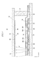
- FIG. 1 is a partial sectional view of a light emission device according to a first embodiment of the present invention.
- FIG. 2 is a partially exploded perspective view of the light emission device of FIG. 1.
- FIG. 3 is a partial sectional view of a light emission device according to a second embodiment of the present invention.
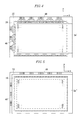
- FIG. 4 is a top plan view of an electron emission unit and a first substrate of a light emission device according to a third embodiment of the present invention.
- FIG. 5 is a top plan view of an electron emission unit and a first substrate of a light emission device according to a fourth embodiment of the present invention.
- FIG. 6 is a partially cut-away perspective view of a light emission device according to a fifth embodiment of the present invention.
- In exemplary embodiments of the present invention, a light emission device can be referred to as a device for emitting light to an exterior thereof. In more detail, the light emission device may be used for transmitting information by displaying symbols, letters, numbers, and/or images. In addition, the light emission device may be used as a light source for emitting light to a passive-type display panel.
- Referring to FIGs. 1 and 2, a
light emission device 10 of a first embodiment of the present invention includes afirst substrate 12 and asecond substrate 14 facing thefirst substrate 12. Thefirst substrate 12 and thesecond substrate 14 are spaced apart from each other by a certain (or predetermined) distance. A sealingmember 16 is provided at peripheries (or peripheral regions) of thefirst substrate 12 and thesecond substrate 14 to seal them together, thereby forming avacuum vessel 18. An interior of thevacuum vessel 18 is exhausted (or evacuated) such that a vacuum (or vacuum pressure) of about 10-6 Torr is maintained. - An
electron emission unit 20 for emitting electrons toward thesecond substrate 14 is formed on an inner surface of thefirst substrate 12, and alight emission unit 22 is provided on an inner surface of thesecond substrate 14. Thefirst substrate 12 may form a rear substrate of thelight emission device 10, and thesecond substrate 14 may form a front substrate of thelight emission device 10. - The
electron emission unit 20 includes a plurality ofcathode electrodes 24, a plurality ofgate electrodes 26, and a plurality ofelectron emission regions 28 that are electrically connected to thecathode electrodes 24. - The
cathode electrodes 24 are arranged in a stripe pattern extending along a first direction (e.g., a y-axis in FIG. 2) on thefirst substrate 12. Afirst insulation layer 30 is formed on an entire surface of thefirst substrate 12 to cover thecathode electrodes 24. Thegate electrodes 26 are formed on thefirst insulation layer 30 and arranged in a stripe pattern extending along a second direction perpendicular to the first direction. That is, thegate electrodes 26 are disposed to cross thecathode electrodes 24. - Each crossing region of the
cathode electrodes 24 and thegate electrodes 26 may correspond to a pixel region of thelight emission device 10.Openings 261 andopenings 301, which correspond to the respective pixel regions, are respectively formed in thegate electrodes 26 and thefirst insulation layer 30 to expose a surface of thecathode electrodes 24. Theelectron emission regions 28 are located on thecathode electrodes 24 at (or in) theopenings 301 of thefirst insulation layer 30. - The
electron emission regions 28 may be formed of a material, which emits electrons when an electric field is applied thereto in a vacuum atmosphere (or pressure). By way of example, the material may be a carbonaceous material and/or a nanometer-sized material. For example, theelectron emission regions 28 may be formed of carbon nanotubes, graphite, graphite nanofibers, diamonds, diamond-like carbon, fullerene (e.g., C60), silicon nanowires, or combinations thereof. Theelectron emission regions 28 may be formed by direct growth, a screen-printing process, chemical vapor deposition, and/or a sputtering process. - Alternatively, the
electron emission regions 28 may be formed to have a tip-like structure. Here, theelectron emission regions 28 may be formed of a Mo-based and/or a Si-based material. Alternatively, as shown in FIG. 2, circular-shapedelectron emission regions 28 are arranged along a length of one (or more) of thecathode electrodes 24. However, embodiments of the present invention are not limited thereto. That is, the shape, number, and arrangement of theelectron emission regions 28 may vary. - A
second insulation layer 32 is formed on thefirst insulation layer 30 to cover thegate electrodes 26. Aheat dissipation layer 34 is formed on thesecond insulation layer 32. Theheat dissipation layer 34 defines an uppermost layer of theelectron emission unit 20 and is adapted to dissipate heat generated from (or by) theelectron emission unit 20 and direct the heat to an exterior of thelight emission device 10. To achieve this, theheat dissipation layer 34 is formed of a material having a relatively high thermal conductivity, for example, of at least 2W/cmK. As shown in FIG. 1, a portion of theheat dissipation layer 34 extends out of thevacuum vessel 18 at a region between the sealingmember 16 and thefirst substrate 12 such that an end portion of theheat dissipation layer 34 is exposed to air outside of thevacuum vessel 18. -
Openings 321 andopenings 341, through which electron beams emitted from theelectron emission regions 28 pass, are respectively formed in thesecond insulation layer 32 and theheat dissipation layer 34. Theheat dissipation layer 34 may include a material selected from the group consisting of silver (Ag), copper (Cu), gold (Au), platinum (Pt), aluminum (Al), and combinations thereof. - The
light emission unit 22 includes aphosphor layer 36 and ananode electrode 38. Thephosphor layer 36 may be a phosphor mixed layer (e.g., a phosphor mixed layer having red, green and blue phosphors) for emitting white light. Here, thephosphor layer 36 may be formed on an entire active area of thesecond substrate 14 or formed to have a plurality of sections corresponding to the pixel regions. Thelight emission device 10 having thephosphor layer 36 may be used as a light source for emitting light to a passive-type display panel. - Alternatively, the
phosphor layer 36 may include red, green, and blue phosphor layers corresponding to the respective pixel regions. Here, as shown in FIGs. 1 and 2, ablack layer 40 for enhancing a contrast of an image may be formed between the red, green and blue phosphor layers of thephosphor layer 36. Here, thelight emission device 10 can be used as a display for displaying one or more images. - The
anode electrode 38 is formed on thephosphor layer 36. Theanode electrode 38 may be a metal layer formed of aluminum (Al), for example. Theanode electrode 38 places thephosphor layer 36 in a high potential state by receiving a voltage for accelerating electron beams and enhances a screen luminance by reflecting visible light radiated from thephosphor layer 36 to thefirst substrate 12 back toward thesecond substrate 14. - Alternatively, the
anode electrode 38 may be a transparent conductive layer formed of, for example, indium tin oxide (ITO). Here, theanode electrode 38 is located between thesecond substrate 14 and thephosphor layer 36. Alternatively, theanode electrode 38 may include both a transparent conductive layer and a metal layer. - Disposed between the
first substrate 12 and thesecond substrate 14 are spacers 42 (see, for example, FIG. 2) for countering a compression force applied to thevacuum vessel 18 and uniformly maintaining a gap between thefirst substrate 12 and thesecond substrate 14. In one embodiment, thespacers 42 are formed of a dielectric material such as glass and/or ceramic. Bottom surfaces of thespacers 42 contact theheat dissipation layer 34. In an embodiment in which thelight emission unit 22 includes ablack layer 40, thespacers 42 are located corresponding to a positioning of theblack layer 40 such that thespacers 42 do not interfere with the light emission of thephosphor layer 36. - The above-described
light emission device 10 is driven when driving voltages (which may be predetermined) are applied to thecathode electrodes 24, thegate electrodes 26, and theanode electrode 38. By way of example, one of thecathode electrodes 24 is applied with a scan driving voltage to serve as a scan driving electrode, and one of thegate electrodes 26 is applied with a data driving voltage to serve as a data driving electrode (or vice versa). Theanode electrode 38 receives an anode voltage for accelerating the electron beams. The anode voltage may be a positive direct current (DC) voltage in a range from hundreds to thousands of volts. - Accordingly, electric fields are formed at (or around) the
electron emission regions 28 at pixels (or pixel regions) where a voltage difference between thecathode electrodes 24 and thegate electrodes 26 is equal to or higher than a threshold value, and electrons are emitted from theelectron emission regions 28. The emitted electrons collide with a corresponding portion of thephosphor layer 36 of the corresponding pixel by being attracted to the anode voltage applied to theanode electrode 38, thereby exciting the corresponding portion of thephosphor layer 36. A light emission intensity of (or at) a portion of thephosphor layer 36 corresponding to a pixel corresponds to an amount of electron beams emitted from the pixel. - When the
light emission device 10 is driven for many hours, heat is generated from thecathode electrodes 24 and thegate electrodes 26, and thus theelectron emission unit 20 may become over-heated. Here, since theheat dissipation layer 34 is formed at the uppermost layer of theelectron emission unit 20, the heat generated from theelectron emission unit 20 may be quickly dissipated (or directed away) through an end portion of theheat dissipation layer 34 exposed to air outside of thevacuum vessel 18. - Therefore, the
light emission device 10 suppresses (or reduces) over-heating of thevacuum vessel 18 to increase (or enhance) a driving stability thereof. In addition, since a temperature of thefirst substrate 12 can be reduced by theheat dissipation layer 34, a temperature difference between thefirst substrate 12 and thesecond substrate 14 can also be reduced. As a result, a surface electric potential variation of thespacer 42 along a height of thespacer 42 can be suppressed (or reduced) and thus electron beam path distortion at (or around) thespacers 42 can be reduced (or minimized), thereby reducing an abnormal light emission at (or around) thespacers 42. - In addition, since the
heat dissipation layer 34 may have a certain electric conductivity as well as a relatively high thermal conductivity, theheat dissipation layer 34 may serve as a focusing electrode. That is, the heat dissipation layer may receive a voltage (e.g., a DC voltage of 0V or a negative DC voltage in a range from several to tens of volts) for focusing an electron beam such that electrons are converged toward a central portion of a bundle of electron beams. - Referring to FIG. 3, a light emission device 10' according to a second embodiment of the present invention includes a focusing
electrode 44 located between thesecond insulation layer 32 and theheat dissipation layer 34. - Electron
beam passing openings 441 are formed in the focusingelectrode 44. The focusingelectrode 44 receives a voltage for focusing electron beams. The focusingelectrode 44 may include a material selected from the group consisting of molybdenum (Mo), chromium (Cr), and combinations thereof. - A top plan shape of the
heat dissipation layer 34 will now be described in more detail with reference to FIGs. 4, 5, and 6. - Referring to FIG. 4, a light emission device according to a third embodiment of the present invention includes a
cathode pad portion 46 located at a first peripheral portion of the first substrate 12 (e.g., an upper edge of thefirst substrate 12 in FIG. 4) and agate pad portion 48 extending from thegate electrodes 26 and located at a second peripheral portion of the first substrate (e.g., a left edge of thefirst substrate 12 in FIG. 4). - A heat dissipation layer 34' is located on an entire active area of the
first substrate 12. The heat dissipation layer 34' has a pair of longitudinal sides (or ends) extending along a first direction (e.g. the y-axis in FIG. 4) and a pair of lateral sides (or ends) extending along a second direction (e.g. the x-axis in FIG. 4). At least one of the lateral sides extends to a third peripheral portion of the first substrate 12 (e.g., a right edge of thefirst substrate 12 in FIG. 4) where thecathode pad portions 46 and thegate pad portions 48 are not located such that the lateral side can be exposed to air outside of thevacuum vessel 18. - Referring to FIG. 5, a light emission device according to a fourth embodiment of the present invention is shown. A
heat dissipation layer 34" has a pair of longitudinal edges and a pair of lateral edges, all of which extend out of the vacuum vessel at a respective region between the sealingmember 16 and thefirst substrate 12. Here, a portion of the second insulation layer (e.g., layer 32) is located under an exposed portion of theheat dissipation layer 34" (see, for example, FIG. 3) to prevent a short circuit between thecathode pad portion 46 and theheat dissipation layer 34". The larger the exposed portion of theheat dissipation layer 34" is, the higher the heat dissipation effect will be. - Referring to FIG. 6, a light emission device according to a fifth embodiment of the present invention is shown. A plurality of
heat dissipation projections 50 are formed along an exposed portion of thesecond insulation layer 32. However, embodiments of the present invention are not limited thereto. That is, the heat dissipation projection may have any of various suitable shapes. - While the present invention has been described in connection with certain exemplary embodiments, it is to be understood that the invention is not limited to the disclosed embodiments, but, on the contrary, is intended to cover various modifications and equivalent arrangements included within the scope of the appended claims.
Claims (16)
- A light emission device comprising:a vacuum vessel including first and second substrates facing each other and a sealing member for sealing the first and second substrates;an electron emission unit located on an inner surface of the first substrate and including a plurality of electron emission regions and a plurality of driving electrodes for controlling electron emission of the electron emission regions;a light emission unit located on an inner surface of the second substrate; anda heat dissipation layer defining an upper layer of the electron emission unit and having a relatively high thermal conductivity, a portion of the heat dissipation layer extending out of the vacuum vessel through a region between the sealing member and the first substrate.
- The light emission device of claim 1, wherein the relatively high thermal conductivity comprises at least 2W/cmK.
- The light emission device of claim 1 or 2, wherein the heat dissipation layer includes a material selected from the group consisting of silver (Ag), copper (Cu), platinum (Pt), aluminum (Al), and combinations thereof.
- The light emission device of any one of the preceding claims, further comprising an insulation layer located between the driving electrodes and the heat dissipation layer, wherein a portion of the insulation layer extends out of the vacuum vessel through a region between the heat dissipation layer and the first substrate.
- The light emission device of any one of the preceding claims,
wherein the heat dissipation layer includes a pair of longitudinal edges and a pair of lateral edges, and
wherein at least one edge of the pair of longitudinal edges or the pair of lateral edges is located outside the vacuum vessel. - The light emission device of claim 5, wherein the at least one edge comprises a plurality of heat dissipation projections.
- The light emission device of any one of the preceding claims, wherein the heat dissipation layer comprises a driving electrode.
- The light emission device of claim 7, wherein the driving electrode comprises a focusing electrode for focusing electron beams.
- The light emission device of any one of claims 1 to 6, wherein the driving electrodes include:a plurality of cathode electrodes;a plurality of gate electrodes located above the cathode electrodes and crossing the cathode electrodes, a first insulation layer being interposed between the cathode electrodes and the gate electrodes; anda focusing electrode located above the gate electrodes, a second insulation layer being interposed between the focusing electrode and the gate electrodes,wherein the heat dissipation layer is formed on the focusing electrode.
- The light emission device of claim 9,
wherein the focusing electrode includes a material selected from the group consisting of chromium (Cr), molybdenum (Mo), and combinations thereof. - The light emission device of claim 9 or 10, wherein a portion of the second insulation layer extends out of the vacuum vessel at a region between the heat dissipation layer and the first substrate.
- The light emission device of any one of the preceding claims, wherein the light emission unit includes a phosphor layer for emitting white light and an anode electrode located on a surface of the phosphor layer.
- The light emission device of any one of the preceding claims, wherein the light emission unit includes red, green, and blue phosphor layers spaced apart from each other, a black layer located between at least two of the red, green, and blue phosphor layers, and an anode electrode located on respective surfaces of the red, green, and blue phosphor layers and the black layer.
- The light emission device of claim 13, further comprising at least one spacer located between the light emission unit and the heat dissipation layer, the location of the at least one spacer corresponding to a positioning of the black layer.
- The light emission device of any one of the preceding claims, wherein the electron emission regions comprise a material selected from the group consisting of carbon nanotubes, graphite, graphite nanofibers, diamonds, diamond-like carbon, fullerene (C60), silicon nanowires, and combinations thereof.
- The light emission device of any one of the preceding claims, wherein the heat dissipation layer is in contact with a plurality of spacers located between the electron emission unit and the light emission unit.
Applications Claiming Priority (2)
| Application Number | Priority Date | Filing Date | Title |
|---|---|---|---|
| KR1020060016413A KR20070083121A (en) | 2006-02-20 | 2006-02-20 | Electron emission indicator |
| KR1020060102322A KR20080035807A (en) | 2006-10-20 | 2006-10-20 | Light emitting device |
Publications (1)
| Publication Number | Publication Date |
|---|---|
| EP1821334A2 true EP1821334A2 (en) | 2007-08-22 |
Family
ID=37955239
Family Applications (1)
| Application Number | Title | Priority Date | Filing Date |
|---|---|---|---|
| EP07102402A Withdrawn EP1821334A2 (en) | 2006-02-20 | 2007-02-14 | Light emission device having an electron emission unit with driving electrodes |
Country Status (2)
| Country | Link |
|---|---|
| US (1) | US20070200483A1 (en) |
| EP (1) | EP1821334A2 (en) |
Cited By (1)
| Publication number | Priority date | Publication date | Assignee | Title |
|---|---|---|---|---|
| EP1916700A3 (en) * | 2006-10-27 | 2010-02-24 | Samsung SDI Co., Ltd. | Light emission device and display device using the light emission device |
Families Citing this family (1)
| Publication number | Priority date | Publication date | Assignee | Title |
|---|---|---|---|---|
| CN106784390A (en) * | 2017-03-06 | 2017-05-31 | 京东方科技集团股份有限公司 | Substrate for display panel and preparation method thereof, display panel and method for packing |
Family Cites Families (4)
| Publication number | Priority date | Publication date | Assignee | Title |
|---|---|---|---|---|
| JP4119279B2 (en) * | 2003-02-21 | 2008-07-16 | 株式会社 日立ディスプレイズ | Display device |
| KR100918044B1 (en) * | 2003-05-06 | 2009-09-22 | 삼성에스디아이 주식회사 | Field emission indicator |
| KR20050086238A (en) * | 2004-02-25 | 2005-08-30 | 삼성에스디아이 주식회사 | Field emission display device |
| JP2006073516A (en) * | 2004-08-30 | 2006-03-16 | Samsung Sdi Co Ltd | Electron emitting device and manufacturing method thereof |
-
2007
- 2007-02-14 EP EP07102402A patent/EP1821334A2/en not_active Withdrawn
- 2007-02-16 US US11/707,574 patent/US20070200483A1/en not_active Abandoned
Cited By (1)
| Publication number | Priority date | Publication date | Assignee | Title |
|---|---|---|---|---|
| EP1916700A3 (en) * | 2006-10-27 | 2010-02-24 | Samsung SDI Co., Ltd. | Light emission device and display device using the light emission device |
Also Published As
| Publication number | Publication date |
|---|---|
| US20070200483A1 (en) | 2007-08-30 |
Similar Documents
| Publication | Publication Date | Title |
|---|---|---|
| US7382089B2 (en) | Field emission display having damage prevention anode input terminal layers | |
| KR100884527B1 (en) | Field emission indicator | |
| JP2004207204A (en) | Field emission display | |
| US20070096624A1 (en) | Electron emission device | |
| US20070200483A1 (en) | Light emission device | |
| US7569986B2 (en) | Electron emission display having electron beams with reduced distortion | |
| EP1780751B1 (en) | Spacer and electron emission display including the spacer | |
| EP1780752B1 (en) | Spacer and electron emission display having the same | |
| KR20080088884A (en) | Light emission device | |
| US7573187B2 (en) | Electron emission device and electron emission display having the electron emission device | |
| KR100898286B1 (en) | Field emission display prevents diode emission | |
| US20080088220A1 (en) | Electron emission device | |
| CN100533647C (en) | Electron emission display device | |
| CN101026076A (en) | Light emission device | |
| US7880383B2 (en) | Electron emission display | |
| US20070267638A1 (en) | Light emission device and electron emission display | |
| KR20070047455A (en) | Electron emission indicator | |
| EP1780753B1 (en) | Electron emission display | |
| KR20070014680A (en) | Electron-emitting device | |
| KR20070083120A (en) | Electron emission indicator | |
| US20070262697A1 (en) | Electron emission device and light emission device including the electron emission device | |
| KR20080036762A (en) | Electron emission display | |
| KR20070024137A (en) | Vacuum flatbed devices | |
| KR20080035807A (en) | Light emitting device | |
| KR20060088217A (en) | Electron-emitting device |
Legal Events
| Date | Code | Title | Description |
|---|---|---|---|
| PUAI | Public reference made under article 153(3) epc to a published international application that has entered the european phase |
Free format text: ORIGINAL CODE: 0009012 |
|
| 17P | Request for examination filed |
Effective date: 20070214 |
|
| AK | Designated contracting states |
Kind code of ref document: A2 Designated state(s): AT BE BG CH CY CZ DE DK EE ES FI FR GB GR HU IE IS IT LI LT LU LV MC NL PL PT RO SE SI SK TR |
|
| AX | Request for extension of the european patent |
Extension state: AL BA HR MK YU |
|
| RAP1 | Party data changed (applicant data changed or rights of an application transferred) |
Owner name: SAMSUNG SDI CO., LTD. |
|
| STAA | Information on the status of an ep patent application or granted ep patent |
Free format text: STATUS: THE APPLICATION HAS BEEN WITHDRAWN |
|
| 18W | Application withdrawn |
Effective date: 20101203 |