EP1818991A2 - Nitride-based semiconductor light emitting device and method of manufacturing the same - Google Patents
Nitride-based semiconductor light emitting device and method of manufacturing the same Download PDFInfo
- Publication number
- EP1818991A2 EP1818991A2 EP06118864A EP06118864A EP1818991A2 EP 1818991 A2 EP1818991 A2 EP 1818991A2 EP 06118864 A EP06118864 A EP 06118864A EP 06118864 A EP06118864 A EP 06118864A EP 1818991 A2 EP1818991 A2 EP 1818991A2
- Authority
- EP
- European Patent Office
- Prior art keywords
- clad layer
- layer
- nitride
- posts
- nano
- Prior art date
- Legal status (The legal status is an assumption and is not a legal conclusion. Google has not performed a legal analysis and makes no representation as to the accuracy of the status listed.)
- Withdrawn
Links
Images


Classifications
-
- H—ELECTRICITY
- H10—SEMICONDUCTOR DEVICES; ELECTRIC SOLID-STATE DEVICES NOT OTHERWISE PROVIDED FOR
- H10H—INORGANIC LIGHT-EMITTING SEMICONDUCTOR DEVICES HAVING POTENTIAL BARRIERS
- H10H20/00—Individual inorganic light-emitting semiconductor devices having potential barriers, e.g. light-emitting diodes [LED]
- H10H20/80—Constructional details
- H10H20/81—Bodies
- H10H20/819—Bodies characterised by their shape, e.g. curved or truncated substrates
- H10H20/82—Roughened surfaces, e.g. at the interface between epitaxial layers
-
- A—HUMAN NECESSITIES
- A61—MEDICAL OR VETERINARY SCIENCE; HYGIENE
- A61H—PHYSICAL THERAPY APPARATUS, e.g. DEVICES FOR LOCATING OR STIMULATING REFLEX POINTS IN THE BODY; ARTIFICIAL RESPIRATION; MASSAGE; BATHING DEVICES FOR SPECIAL THERAPEUTIC OR HYGIENIC PURPOSES OR SPECIFIC PARTS OF THE BODY
- A61H39/00—Devices for locating or stimulating specific reflex points of the body for physical therapy, e.g. acupuncture
- A61H39/04—Devices for pressing such points, e.g. Shiatsu or Acupressure
-
- A—HUMAN NECESSITIES
- A61—MEDICAL OR VETERINARY SCIENCE; HYGIENE
- A61H—PHYSICAL THERAPY APPARATUS, e.g. DEVICES FOR LOCATING OR STIMULATING REFLEX POINTS IN THE BODY; ARTIFICIAL RESPIRATION; MASSAGE; BATHING DEVICES FOR SPECIAL THERAPEUTIC OR HYGIENIC PURPOSES OR SPECIFIC PARTS OF THE BODY
- A61H15/00—Massage by means of rollers, balls, e.g. inflatable, chains, or roller chains
- A61H15/0092—Massage by means of rollers, balls, e.g. inflatable, chains, or roller chains hand-held
-
- H—ELECTRICITY
- H10—SEMICONDUCTOR DEVICES; ELECTRIC SOLID-STATE DEVICES NOT OTHERWISE PROVIDED FOR
- H10H—INORGANIC LIGHT-EMITTING SEMICONDUCTOR DEVICES HAVING POTENTIAL BARRIERS
- H10H20/00—Individual inorganic light-emitting semiconductor devices having potential barriers, e.g. light-emitting diodes [LED]
- H10H20/80—Constructional details
- H10H20/81—Bodies
- H10H20/814—Bodies having reflecting means, e.g. semiconductor Bragg reflectors
-
- A—HUMAN NECESSITIES
- A61—MEDICAL OR VETERINARY SCIENCE; HYGIENE
- A61H—PHYSICAL THERAPY APPARATUS, e.g. DEVICES FOR LOCATING OR STIMULATING REFLEX POINTS IN THE BODY; ARTIFICIAL RESPIRATION; MASSAGE; BATHING DEVICES FOR SPECIAL THERAPEUTIC OR HYGIENIC PURPOSES OR SPECIFIC PARTS OF THE BODY
- A61H15/00—Massage by means of rollers, balls, e.g. inflatable, chains, or roller chains
- A61H2015/0007—Massage by means of rollers, balls, e.g. inflatable, chains, or roller chains with balls or rollers rotating about their own axis
- A61H2015/0014—Massage by means of rollers, balls, e.g. inflatable, chains, or roller chains with balls or rollers rotating about their own axis cylinder-like, i.e. rollers
-
- A—HUMAN NECESSITIES
- A61—MEDICAL OR VETERINARY SCIENCE; HYGIENE
- A61H—PHYSICAL THERAPY APPARATUS, e.g. DEVICES FOR LOCATING OR STIMULATING REFLEX POINTS IN THE BODY; ARTIFICIAL RESPIRATION; MASSAGE; BATHING DEVICES FOR SPECIAL THERAPEUTIC OR HYGIENIC PURPOSES OR SPECIFIC PARTS OF THE BODY
- A61H2201/00—Characteristics of apparatus not provided for in the preceding codes
- A61H2201/10—Characteristics of apparatus not provided for in the preceding codes with further special therapeutic means, e.g. electrotherapy, magneto therapy or radiation therapy, chromo therapy, infrared or ultraviolet therapy
-
- A—HUMAN NECESSITIES
- A61—MEDICAL OR VETERINARY SCIENCE; HYGIENE
- A61H—PHYSICAL THERAPY APPARATUS, e.g. DEVICES FOR LOCATING OR STIMULATING REFLEX POINTS IN THE BODY; ARTIFICIAL RESPIRATION; MASSAGE; BATHING DEVICES FOR SPECIAL THERAPEUTIC OR HYGIENIC PURPOSES OR SPECIFIC PARTS OF THE BODY
- A61H2201/00—Characteristics of apparatus not provided for in the preceding codes
- A61H2201/16—Physical interface with patient
- A61H2201/1683—Surface of interface
- A61H2201/169—Physical characteristics of the surface, e.g. material, relief, texture or indicia
-
- H—ELECTRICITY
- H10—SEMICONDUCTOR DEVICES; ELECTRIC SOLID-STATE DEVICES NOT OTHERWISE PROVIDED FOR
- H10H—INORGANIC LIGHT-EMITTING SEMICONDUCTOR DEVICES HAVING POTENTIAL BARRIERS
- H10H20/00—Individual inorganic light-emitting semiconductor devices having potential barriers, e.g. light-emitting diodes [LED]
- H10H20/80—Constructional details
- H10H20/81—Bodies
- H10H20/822—Materials of the light-emitting regions
- H10H20/824—Materials of the light-emitting regions comprising only Group III-V materials, e.g. GaP
- H10H20/825—Materials of the light-emitting regions comprising only Group III-V materials, e.g. GaP containing nitrogen, e.g. GaN
-
- H—ELECTRICITY
- H10—SEMICONDUCTOR DEVICES; ELECTRIC SOLID-STATE DEVICES NOT OTHERWISE PROVIDED FOR
- H10H—INORGANIC LIGHT-EMITTING SEMICONDUCTOR DEVICES HAVING POTENTIAL BARRIERS
- H10H20/00—Individual inorganic light-emitting semiconductor devices having potential barriers, e.g. light-emitting diodes [LED]
- H10H20/80—Constructional details
- H10H20/872—Periodic patterns for optical field-shaping, e.g. photonic bandgap structures
Definitions
- the present invention relates to a semiconductor light emitting device, and more particularly, to a nitride-based semiconductor light emitting device having an improved structure in which light extraction efficiency is improved, and a method of manufacturing the same.
- Light emitting devices such as light emitting diodes (LED) are basically semiconductor PN junction diodes. Silicon PN junction plays a leading role of electronic information revolution, and PN junction of a III-V group compound semiconductor plays a leading role of light revolution.
- the III-V group compound semiconductor is made by combining III- and V-group elements on an element periodic table. It has an advantage of luminous efficiency that is almost close to 100%. This luminous efficiency is approximately ten hundreds times higher than silicon. Thus, LED are widely used in a light emitting device such as a diode laser, from the initial stage of development of a material and plays a leading role of optical revolution.
- LED since LED have a higher movement speed of electrons and can operate at a high temperature, it is widely used in high-speed and high-power electronic devices.
- III- and V-group elements are mixed with one another so that a semiconductor having a variety of material composition and characteristics can be manufactured.
- luminosity units: candela (cd)
- radiant flux units: watt
- Luminosity is indicated by light velocity per unit cubic angle
- brightness is indicated by luminosity per unit area.
- a photometer is used to measure luminosity.
- Radiant flux represents all power radiated from all wavelengths of an LED and is indicated by energy radiated per unit time.
- Luminous efficiency of an LED can be mainly determined by three factors, such as internal quantum efficiency, extraction efficiency, and operating voltage. Research for improvement of luminous efficiency has been currently developed.
- LEDs In general, conventional LEDs have a sapphire/n-GaN/MQW/p-GaN structure. However, in such LEDs, defect density is high due to limitations of manufacture technology. Thus, there are limitations in addressing current technical objects, that is, a first object for improving internal quantum efficiency of an MQW layer and a second object for manufacturing a high-power LED. Accordingly, the structure of an LED need to be improved so that the limitations can be overcome and external extraction efficiency of light can be increased.
- a nitride-based semiconductor light emitting device comprising an n-clad layer, an active layer, and a p-clad layer, which are sequentially stacked on a substrate, wherein the n-clad layer comprises a first clad layer, a second clad layer, and a light extraction layer interposed between the first clad layer and the second clad layer and composed of an array of a plurality of nano-posts, the light extraction layer diffracting or/and scattering light generated in the active layer.
- the present invention provides a nitride-based semiconductor light emitting device having an improved structure in which light extraction efficiency is improved, and a method of manufacturing the same.
- the nano-posts may be formed of a material having a different refraction index from a material used in forming the first clad layer and the second clad layer.
- the nano-posts may be formed of a light transmission material having a refraction index of 2.5 and less.
- the nano-posts may be formed of a transparent material with respect to a wavelength in a range of 200-780 nm.
- the nano-posts may be formed of a material selected from the group consisting of SiO 2 , SiN x , Al 2 O 3 , HfO, TiO 2 , ZrO, and ZnO or by adding a material selected from the group consisting of Mg, Ag, Zn, Sc, Hf, Zr, Te, Se, Ta, W, Nb, Cu, Si, Ni, Co, Mo, Cr, Mn, Hg, Pr, and La to an indium oxide.
- the first clad layer and the second clad layer may be formed of an AllnGaN-based lll-V-group nitride semiconductor material.
- the first clad layer and the second clad layer may be formed of substantially the same material.
- An arrangement period of the nano-posts may be 100-2000 nm, for example, 700 nm.
- a height of each of the nano-posts may be 100-1000 nm, for example, 300 nm.
- a diameter of each of the nano-posts may be 100-1000 nm.
- a method of manufacturing a nitride-based semiconductor light emitting device comprising sequentially forming an n-clad layer, an active layer, and a p-clad layer on a substrate, wherein the forming of the n-clad layer comprises: forming a first clad layer on the substrate; forming a light transmission material layer on the first clad layer; patterning the light transmission material layer to form a light extraction layer composed of an array of a plurality of nano-posts and diffracting or/and scattering light generated in the active layer; and forming a second clad layer for embedding the light extraction layer on the first clad layer.
- the patterning of the light transmission material layer may be performed using a hologram lithography method.
- the light transmission material layer may be formed of a material having a different refraction index from a material used in forming the first clad layer and the second clad layer.
- the light transmission material layer may be formed of a light transmission material having a refraction index of 2.5 and less.
- the light transmission material layer may be formed of a transparent material with respect to a wavelength in a range of 200-780 nm.
- the light transmission material layer may be formed of a material selected from the group consisting of SiO 2 , SiN x , Al 2 O 3 , HfO, TiO 2 , ZrO, and ZnO or by adding a material selected from the group consisting of Mg, Ag, Zn, Sc, Hf, Zr, Te, Se, Ta, W, Nb, Cu, Si, Ni, Co, Mo, Cr, Mn, Hg, Pr, and La to an indium oxide.
- the first clad layer and the second clad layer may be formed of an AllnGaN-based lll-V-group nitride semiconductor material.
- the first clad layer and the second clad layer may be formed of substantially the same material.
- An arrangement period of the nano-posts may be 100-2000 nm, for example, 700 nm.
- a height of each of the nano-posts may be 100-1000 nm, for example, 300 nm.
- a diameter of each of the nano-posts may be 100-1000 nm.
- a nitride-based semiconductor light emitting device having an improved structure in which light extraction efficiency is improved can be obtained.
- FIG. 1 is a cross-sectional view of a nitride-based semiconductor light emitting device according to an embodiment of the present invention.
- the nitride-based semiconductor light emitting device includes an n-clad layer 20, an active layer 40, and a p-clad layer 50, which are sequentially stacked on a substrate 10.
- the n-clad layer 20 includes a first clad layer 12, a second clad layer 14, and a light extraction layer 30a composed of an array of a plurality of nano-posts interposed between the first clad layer 12 and the second clad layer 14.
- An n-electrode 100 and a p-electrode 200 are formed on an etched surface of the n-clad layer 20 and on the p-clad layer 50, respectively.
- the substrate 10 may be one of Si, GaAs, SiC, GaN, and sapphire substrates.
- the n-clad layer 20 may be formed of an AllnGaN-based III-V-group nitride semiconductor material, for example, an n-GaN layer.
- the p-clad layer 50 may be formed of a p-GaN-based lll-V-group nitride semiconductor layer, for example, a p-GaN layer or a p-GaN/AIGaN layer.
- the active layer 40 may be formed of a GaN-based lll-V-group nitride semiconductor layer which is In x Al y Ga 1-x-y N(0 ⁇ x ⁇ 1, 0 ⁇ y ⁇ 1 and 0 ⁇ x+y ⁇ 1), for example, an InGaN layer or an AlGaN layer.
- the active layer 40 may have one structure of a multi-quantum well (MQW) or a single quantum well.
- MQW multi-quantum well
- the structure of the active layer 40 does not restrict the technical scope of the present invention.
- the active layer 40 may be formed of GaN/lnGaN/GaN MQW or GaN/AlGaN/GaN MQW.
- the nitride-based semiconductor light emitting device having the above structure, if a predetermined voltage is applied between the n-electrode 100 and the p-electrode 200, electrons and holes are injected into the active layer 40 from the n-clad layer 20 and the p-clad layer 50, respectively, and combined in the active layer 40 so that light can be outputted from the active layer 40.
- the n-clad layer 20 includes the first clad layer 12, the second clad layer 14, and the light extraction layer 30a composed of an array of a plurality of nano-posts interposed between the first clad layer 12 and the second clad layer 14.
- the light extraction layer 30a can perform the function of increasing external extraction efficiency of light by diffracting or/and scattering light generated in the active layer 40.
- an arrangement period of the nano-posts is 100-2000 nm and may be 700 nm.
- a height of each of the nano-posts is 100-1000 nm and may be 300 nm.
- a diameter of each of the nano-posts may be 100-1000 nm.
- the first clad layer 12 and the second clad layer 14 are formed of an AllnGaN-based III-V-group nitride semiconductor material.
- the first clad layer 12 and the second clad layer 14 may be formed of substantially the same material, for example, an n-GaN material.
- the nano-posts can be formed of a material having a different refraction index from a material used in forming the first clad layer 12 and the second clad layer 14.
- the nano-posts are formed of a light transmission material having a refraction index of 2.5 and less and may be formed of a transparent material with respect to a wavelength in a range of 200-780 nm.
- the illustrated wavelength range may include a wavelength range of UV and all visible ray regions.
- the nano-posts may be formed of a material selected from the group consisting of SiO 2 , SiN x , Al 2 O 3 , HfO, TiO 2 , ZrO, and ZnO or by adding a material selected from the group consisting of Mg, Ag, Zn, Sc, Hf, Zr, Te, Se, Ta, W, Nb, Cu, Si, Ni, Co, Mo, Cr, Mn, Hg, Pr, and La to an indium oxide.
- an indium oxide to which the material is added there is an indium tin oxide (ITO) or a copper-doped indium oxide (CIO) material.
- ITO indium tin oxide
- CIO copper-doped indium oxide
- the light extraction layer 30a composed of an array of a plurality of nano-posts is embedded in the n-clad layer 20.
- the light extraction layer 30a can increase external extraction efficiency of light by diffracting or/and scattering light generated in the active layer 40.
- FIG. 2 is a graph showing simulation results of light extraction improvement of the nitride-based semiconductor light emitting device illustrated in FIG. 1.
- Graph 1 (dotted line) shows a light output of an LED having a conventional sapphire/n-GaN/MQW/p-GaN structure
- Graph 2 shows a light output of an LED having a conventional epitaxial lateral overgrowth (ELOG) pattern.
- Graph 3 shows a light output of a nitride-based semiconductor light emitting device according to the present invention.
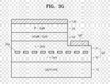
- FIGS. 3A through 3G are flowcharts illustrating a method of manufacturing a nitride-based semiconductor light emitting device according to an embodiment of the present invention.
- the first clad layer 12 is formed on the prepared substrate 10, such as, Si, GaAs, SiC, GaN or sapphire substrate, using the same kind of stacking method, for example, a GaN-based crystalline layer growth on a GaN substrate, or a different kind of stacking method, for example, a GaN-based crystalline growth on a sapphire substrate.
- the first clad layer 12 may be formed of an AllnGaN-based III-V-group nitride semiconductor material, for example, an n-GaN layer.
- a light transmission material layer 30 is formed of a material having a different refraction index from a material used in forming the first clad layer 12 on the first clad layer 12.
- the light transmission material layer 30 may be formed of a light transmission material having a refraction index of 2.5 and less, for example, may be formed of a transparent material with respect to a wavelength in a range of 200-780 nm.
- the illustrated wavelength range may include a wavelength range of UV and all visible ray regions.
- the light transmission material layer 30 may be formed of a material selected from the group consisting of SiO 2 , SiN x , Al 2 O 3 , HfO, TiO 2 , ZrO, and ZnO or by adding a material selected from the group consisting of Mg, Ag, Zn, Sc, Hf, Zr, Te, Se, Ta, W, Nb, Cu, Si, Ni, Co, Mo, Cr, Mn, Hg, Pr, and La to an indium oxide.
- an indium oxide to which the material is added there is an indium tin oxide (ITO) or a copper-doped indium oxide (CIO) material.
- ITO indium tin oxide
- CIO copper-doped indium oxide
- the n-clad layer 20 and the light transmission material layer 30 may be formed using vapor deposition, such as halide or hydride vapor phase epitaxy (HVPE), metal organic chemical vapor deposition (MOCVD), molecular beam epitaxy (MBE), plasma enhanced chemical vapor deposition (PECVD) or evaporation. Since the methods are well-known in the art, a detailed description thereof will be omitted.
- vapor deposition such as halide or hydride vapor phase epitaxy (HVPE), metal organic chemical vapor deposition (MOCVD), molecular beam epitaxy (MBE), plasma enhanced chemical vapor deposition (PECVD) or evaporation. Since the methods are well-known in the art, a detailed description thereof will be omitted.
- the light transmission material layer 30 is patterned, thereby forming the light extraction layer 30a composed of an array of a plurality of nano-posts.
- patterning of the light transmission material layer 30 can be performed using a hologram lithography method.
- the light extraction layer 30a can perform the function of increasing external extraction efficiency of light by diffracting or/and scattering light generated in the active layer 40 which will be formed later.
- an arrangement period of the nano-posts is 100-2000 nm and may be 700 nm.
- a height of each of the nano-posts is 100-1000 nm and may be 300 nm.
- a diameter of each of the nano-posts may be 100-1000 nm.
- the second clad layer 14 for embedding the light extraction layer 30a is formed on the first clad layer 12.
- the second clad layer 14 constitutes the n-clad layer 20 together with the first clad layer 12.
- the second clad layer 14 is formed of an AllnGaN-based III-V-group nitride semiconductor material.
- the second clad layer 14 may be formed of substantially the same material as the first clad layer 12.
- the second clad layer 14 may be formed of an n-GaN layer.
- the second clad layer 14 can be formed using the same method as a method of forming the first clad layer 12, such as, HVPE, MOCVD, MBE, PECVD, sputtering or evaporation.
- the active layer 40 and the p-clad layer 50 are sequentially formed on the second clad layer 14.
- the active layer 40 and the p-clad layer 50 can be formed using vapor deposition such as HVPE, MOCVD or MBE.
- the active layer 40 may be formed of a GaN-based lll-V-group nitride semiconductor layer which is In x Al y Ga 1-x-y N(0 ⁇ x ⁇ 1, 0 ⁇ y ⁇ 1 and 0 ⁇ x+y ⁇ 1), for example, an lnGaN layer or an AlGaN layer.
- the active layer 40 may have one structure of a multi-quantum well (MQW) or a single quantum well.
- MQW multi-quantum well
- the structure of the active layer 40 does not restrict the technical scope of the present invention.
- the active layer 40 may be formed of GaN/lnGaN/GaN MQW or GaN/AlGaN/GaN MQW.
- the p-clad layer 50 may be formed of a p-GaN-based lll-V-group nitride semiconductor layer, for example, a p-GaN layer or a p-GaN/AlGaN layer.
- a top surface of the p-clad layer 50 is etched to a predetermined depth of the n-clad layer 20, thereby forming an etched surface on the n-clad layer 20.
- the n-electrode 100 and the p-electrode 200 are formed of a conductive material, such as Ag, Au or indium tin oxide (ITO), on the etched surface of the n-clad layer 20 and the p-clad layer 50.
- a conductive material such as Ag, Au or indium tin oxide (ITO)
- the nitride-based semiconductor light emitting device having an improved structure in which light extraction efficiency is improved can be obtained.
- the light extraction layer composed of an array of a plurality of nano-posts is embedded in the n-clad layer.
- the light extraction layer can increase external extraction efficiency of light by diffracting or/and scattering light generated in the active layer. Thus, light extraction efficiency can be improved compared to the prior art.
Landscapes
- Health & Medical Sciences (AREA)
- Rehabilitation Therapy (AREA)
- Epidemiology (AREA)
- Pain & Pain Management (AREA)
- Physical Education & Sports Medicine (AREA)
- Life Sciences & Earth Sciences (AREA)
- Animal Behavior & Ethology (AREA)
- General Health & Medical Sciences (AREA)
- Public Health (AREA)
- Veterinary Medicine (AREA)
- Led Devices (AREA)
Abstract
Description
- The present invention relates to a semiconductor light emitting device, and more particularly, to a nitride-based semiconductor light emitting device having an improved structure in which light extraction efficiency is improved, and a method of manufacturing the same.
- Light emitting devices, such as light emitting diodes (LED), are basically semiconductor PN junction diodes. Silicon PN junction plays a leading role of electronic information revolution, and PN junction of a III-V group compound semiconductor plays a leading role of light revolution. The III-V group compound semiconductor is made by combining III- and V-group elements on an element periodic table. It has an advantage of luminous efficiency that is almost close to 100%. This luminous efficiency is approximately ten hundreds times higher than silicon. Thus, LED are widely used in a light emitting device such as a diode laser, from the initial stage of development of a material and plays a leading role of optical revolution. In addition, since LED have a higher movement speed of electrons and can operate at a high temperature, it is widely used in high-speed and high-power electronic devices. In particular, several III- and V-group elements are mixed with one another so that a semiconductor having a variety of material composition and characteristics can be manufactured.
- As basic characteristics of an LED, luminosity (units: candela (cd)) is used in an LED in a visible ray region and radiant flux (units: watt) is used in an invisible ray region. Luminosity is indicated by light velocity per unit cubic angle, and brightness is indicated by luminosity per unit area. A photometer is used to measure luminosity. Radiant flux represents all power radiated from all wavelengths of an LED and is indicated by energy radiated per unit time.
- Main factors for determining a visible ray LED performance are luminous efficiency indicated by lumen per watt (lm/W). This corresponds wall-plug efficiency (optical output/input electric power amount) in consideration of human eyes' luminosity factor. Luminous efficiency of an LED can be mainly determined by three factors, such as internal quantum efficiency, extraction efficiency, and operating voltage. Research for improvement of luminous efficiency has been currently developed.
- In general, conventional LEDs have a sapphire/n-GaN/MQW/p-GaN structure. However, in such LEDs, defect density is high due to limitations of manufacture technology. Thus, there are limitations in addressing current technical objects, that is, a first object for improving internal quantum efficiency of an MQW layer and a second object for manufacturing a high-power LED. Accordingly, the structure of an LED need to be improved so that the limitations can be overcome and external extraction efficiency of light can be increased.
- According to an aspect of the present invention, there is provided a nitride-based semiconductor light emitting device comprising an n-clad layer, an active layer, and a p-clad layer, which are sequentially stacked on a substrate, wherein the n-clad layer comprises a first clad layer, a second clad layer, and a light extraction layer interposed between the first clad layer and the second clad layer and composed of an array of a plurality of nano-posts, the light extraction layer diffracting or/and scattering light generated in the active layer.
- The present invention provides a nitride-based semiconductor light emitting device having an improved structure in which light extraction efficiency is improved, and a method of manufacturing the same.
- The nano-posts may be formed of a material having a different refraction index from a material used in forming the first clad layer and the second clad layer. The nano-posts may be formed of a light transmission material having a refraction index of 2.5 and less. Specifically, the nano-posts may be formed of a transparent material with respect to a wavelength in a range of 200-780 nm. For example, the nano-posts may be formed of a material selected from the group consisting of SiO2, SiNx, Al2O3, HfO, TiO2, ZrO, and ZnO or by adding a material selected from the group consisting of Mg, Ag, Zn, Sc, Hf, Zr, Te, Se, Ta, W, Nb, Cu, Si, Ni, Co, Mo, Cr, Mn, Hg, Pr, and La to an indium oxide. The first clad layer and the second clad layer may be formed of an AllnGaN-based lll-V-group nitride semiconductor material. The first clad layer and the second clad layer may be formed of substantially the same material.
- An arrangement period of the nano-posts may be 100-2000 nm, for example, 700 nm. A height of each of the nano-posts may be 100-1000 nm, for example, 300 nm. A diameter of each of the nano-posts may be 100-1000 nm.
- According to another aspect of the present invention, there is provided a method of manufacturing a nitride-based semiconductor light emitting device, the method comprising sequentially forming an n-clad layer, an active layer, and a p-clad layer on a substrate, wherein the forming of the n-clad layer comprises: forming a first clad layer on the substrate; forming a light transmission material layer on the first clad layer; patterning the light transmission material layer to form a light extraction layer composed of an array of a plurality of nano-posts and diffracting or/and scattering light generated in the active layer; and forming a second clad layer for embedding the light extraction layer on the first clad layer.
- The patterning of the light transmission material layer may be performed using a hologram lithography method.
- The light transmission material layer may be formed of a material having a different refraction index from a material used in forming the first clad layer and the second clad layer.
- The light transmission material layer may be formed of a light transmission material having a refraction index of 2.5 and less. Specifically, the light transmission material layer may be formed of a transparent material with respect to a wavelength in a range of 200-780 nm. For example, the light transmission material layer may be formed of a material selected from the group consisting of SiO2, SiNx, Al2O3, HfO, TiO2, ZrO, and ZnO or by adding a material selected from the group consisting of Mg, Ag, Zn, Sc, Hf, Zr, Te, Se, Ta, W, Nb, Cu, Si, Ni, Co, Mo, Cr, Mn, Hg, Pr, and La to an indium oxide. The first clad layer and the second clad layer may be formed of an AllnGaN-based lll-V-group nitride semiconductor material. The first clad layer and the second clad layer may be formed of substantially the same material.
- An arrangement period of the nano-posts may be 100-2000 nm, for example, 700 nm. A height of each of the nano-posts may be 100-1000 nm, for example, 300 nm. A diameter of each of the nano-posts may be 100-1000 nm.
- According to the present invention, a nitride-based semiconductor light emitting device having an improved structure in which light extraction efficiency is improved can be obtained.
- The above and other aspects of the present invention will become more apparent by describing in detail exemplary embodiments thereof with reference to the attached drawings in which:
- FIG. 1 is a cross-sectional view of a nitride-based semiconductor light emitting device according to an embodiment of the present invention;
- FIG. 2 is a graph showing simulation results of light extraction improvement of the nitride-based semiconductor light emitting device illustrated in FIG. 1; and
- FIGS. 3A through 3G are flowcharts illustrating a method of manufacturing a nitride-based semiconductor light emitting device according to an embodiment of the present invention.
- The present invention will now be described more fully with reference to the accompanying drawings, in which exemplary embodiments of the invention are shown. In the drawings, the thicknesses of layers and regions are exaggerated for clarity.
- FIG. 1 is a cross-sectional view of a nitride-based semiconductor light emitting device according to an embodiment of the present invention. Referring to FIG. 1, the nitride-based semiconductor light emitting device includes an n-
clad layer 20, anactive layer 40, and a p-clad layer 50, which are sequentially stacked on asubstrate 10. In particular, the n-clad layer 20 includes afirst clad layer 12, asecond clad layer 14, and alight extraction layer 30a composed of an array of a plurality of nano-posts interposed between thefirst clad layer 12 and thesecond clad layer 14. An n-electrode 100 and a p-electrode 200 are formed on an etched surface of the n-clad layer 20 and on the p-clad layer 50, respectively. - The
substrate 10 may be one of Si, GaAs, SiC, GaN, and sapphire substrates. The n-clad layer 20 may be formed of an AllnGaN-based III-V-group nitride semiconductor material, for example, an n-GaN layer. The p-clad layer 50 may be formed of a p-GaN-based lll-V-group nitride semiconductor layer, for example, a p-GaN layer or a p-GaN/AIGaN layer. - The
active layer 40 may be formed of a GaN-based lll-V-group nitride semiconductor layer which is InxAlyGa1-x-yN(0≤x≤1, 0≤y≤1 and 0≤x+y≤1), for example, an InGaN layer or an AlGaN layer. Here, theactive layer 40 may have one structure of a multi-quantum well (MQW) or a single quantum well. The structure of theactive layer 40 does not restrict the technical scope of the present invention. For example, theactive layer 40 may be formed of GaN/lnGaN/GaN MQW or GaN/AlGaN/GaN MQW. - In the nitride-based semiconductor light emitting device having the above structure, if a predetermined voltage is applied between the n-
electrode 100 and the p-electrode 200, electrons and holes are injected into theactive layer 40 from the n-cladlayer 20 and the p-cladlayer 50, respectively, and combined in theactive layer 40 so that light can be outputted from theactive layer 40. - According to the present invention, the n-clad
layer 20 includes the first cladlayer 12, the second cladlayer 14, and thelight extraction layer 30a composed of an array of a plurality of nano-posts interposed between the first cladlayer 12 and the second cladlayer 14. Here, thelight extraction layer 30a can perform the function of increasing external extraction efficiency of light by diffracting or/and scattering light generated in theactive layer 40. Here, an arrangement period of the nano-posts is 100-2000 nm and may be 700 nm. A height of each of the nano-posts is 100-1000 nm and may be 300 nm. A diameter of each of the nano-posts may be 100-1000 nm. - The first clad
layer 12 and the second cladlayer 14 are formed of an AllnGaN-based III-V-group nitride semiconductor material. Here, the first cladlayer 12 and the second cladlayer 14 may be formed of substantially the same material, for example, an n-GaN material. The nano-posts can be formed of a material having a different refraction index from a material used in forming the first cladlayer 12 and the second cladlayer 14. Specifically, the nano-posts are formed of a light transmission material having a refraction index of 2.5 and less and may be formed of a transparent material with respect to a wavelength in a range of 200-780 nm. The illustrated wavelength range may include a wavelength range of UV and all visible ray regions. For example, the nano-posts may be formed of a material selected from the group consisting of SiO2, SiNx, Al2O3, HfO, TiO2, ZrO, and ZnO or by adding a material selected from the group consisting of Mg, Ag, Zn, Sc, Hf, Zr, Te, Se, Ta, W, Nb, Cu, Si, Ni, Co, Mo, Cr, Mn, Hg, Pr, and La to an indium oxide. Here, as an example of an indium oxide to which the material is added, there is an indium tin oxide (ITO) or a copper-doped indium oxide (CIO) material. - According to the present invention, the
light extraction layer 30a composed of an array of a plurality of nano-posts is embedded in the n-cladlayer 20. Thelight extraction layer 30a can increase external extraction efficiency of light by diffracting or/and scattering light generated in theactive layer 40. Thus, light extraction efficiency can be improved compared to the prior art. FIG. 2 is a graph showing simulation results of light extraction improvement of the nitride-based semiconductor light emitting device illustrated in FIG. 1. Graph 1 (dotted line) shows a light output of an LED having a conventional sapphire/n-GaN/MQW/p-GaN structure, and Graph 2 (thin solid line) shows a light output of an LED having a conventional epitaxial lateral overgrowth (ELOG) pattern. For a structure of an LED having an ELOG pattern,U.S. Patent No. 6,051,849 may be referred to. Graph 3 (thick solid line) shows a light output of a nitride-based semiconductor light emitting device according to the present invention. - FIGS. 3A through 3G are flowcharts illustrating a method of manufacturing a nitride-based semiconductor light emitting device according to an embodiment of the present invention.
- Referring to FIG. 3A, the first clad
layer 12 is formed on theprepared substrate 10,such as, Si, GaAs, SiC, GaN or sapphire substrate, using the same kind of stacking method, for example, a GaN-based crystalline layer growth on a GaN substrate, or a different kind of stacking method, for example, a GaN-based crystalline growth on a sapphire substrate. The first cladlayer 12 may be formed of an AllnGaN-based III-V-group nitride semiconductor material, for example, an n-GaN layer. Then, a lighttransmission material layer 30 is formed of a material having a different refraction index from a material used in forming the first cladlayer 12 on the first cladlayer 12. Specifically, the lighttransmission material layer 30 may be formed of a light transmission material having a refraction index of 2.5 and less, for example, may be formed of a transparent material with respect to a wavelength in a range of 200-780 nm. The illustrated wavelength range may include a wavelength range of UV and all visible ray regions. For example, the lighttransmission material layer 30 may be formed of a material selected from the group consisting of SiO2, SiNx, Al2O3, HfO, TiO2, ZrO, and ZnO or by adding a material selected from the group consisting of Mg, Ag, Zn, Sc, Hf, Zr, Te, Se, Ta, W, Nb, Cu, Si, Ni, Co, Mo, Cr, Mn, Hg, Pr, and La to an indium oxide. Here, as an example of an indium oxide to which the material is added, there is an indium tin oxide (ITO) or a copper-doped indium oxide (CIO) material. - Here, the n-clad
layer 20 and the lighttransmission material layer 30 may be formed using vapor deposition, such as halide or hydride vapor phase epitaxy (HVPE), metal organic chemical vapor deposition (MOCVD), molecular beam epitaxy (MBE), plasma enhanced chemical vapor deposition (PECVD) or evaporation. Since the methods are well-known in the art, a detailed description thereof will be omitted. - Referring to FIGS. 3B and 3C, the light
transmission material layer 30 is patterned, thereby forming thelight extraction layer 30a composed of an array of a plurality of nano-posts. Here, patterning of the lighttransmission material layer 30 can be performed using a hologram lithography method. Thelight extraction layer 30a can perform the function of increasing external extraction efficiency of light by diffracting or/and scattering light generated in theactive layer 40 which will be formed later. - Here, an arrangement period of the nano-posts is 100-2000 nm and may be 700 nm. A height of each of the nano-posts is 100-1000 nm and may be 300 nm. A diameter of each of the nano-posts may be 100-1000 nm.
- Referring to FIGS. 3D and 3E, the second clad
layer 14 for embedding thelight extraction layer 30a is formed on the first cladlayer 12. The second cladlayer 14 constitutes the n-cladlayer 20 together with the first cladlayer 12. Here, the second cladlayer 14 is formed of an AllnGaN-based III-V-group nitride semiconductor material. The second cladlayer 14 may be formed of substantially the same material as the first cladlayer 12. For example, the second cladlayer 14 may be formed of an n-GaN layer. The second cladlayer 14 can be formed using the same method as a method of forming the first cladlayer 12, such as, HVPE, MOCVD, MBE, PECVD, sputtering or evaporation. - Then, the
active layer 40 and the p-cladlayer 50 are sequentially formed on the second cladlayer 14. Here, theactive layer 40 and the p-cladlayer 50 can be formed using vapor deposition such as HVPE, MOCVD or MBE. - The
active layer 40 may be formed of a GaN-based lll-V-group nitride semiconductor layer which is InxAlyGa1-x-yN(0≤x≤1, 0≤y≤1 and 0≤x+y≤1), for example, an lnGaN layer or an AlGaN layer. Here, theactive layer 40 may have one structure of a multi-quantum well (MQW) or a single quantum well. The structure of theactive layer 40 does not restrict the technical scope of the present invention. For example, theactive layer 40 may be formed of GaN/lnGaN/GaN MQW or GaN/AlGaN/GaN MQW. - The p-clad
layer 50 may be formed of a p-GaN-based lll-V-group nitride semiconductor layer, for example, a p-GaN layer or a p-GaN/AlGaN layer. - Referring to FIGS. 3F and 3G, firstly, a top surface of the p-clad
layer 50 is etched to a predetermined depth of the n-cladlayer 20, thereby forming an etched surface on the n-cladlayer 20. Next, the n-electrode 100 and the p-electrode 200 are formed of a conductive material, such as Ag, Au or indium tin oxide (ITO), on the etched surface of the n-cladlayer 20 and the p-cladlayer 50. The nitride-based semiconductor light emitting device according to the present invention can be manufactured using the above processes. - According to the present invention, the nitride-based semiconductor light emitting device having an improved structure in which light extraction efficiency is improved can be obtained. According to the present invention, the light extraction layer composed of an array of a plurality of nano-posts is embedded in the n-clad layer. The light extraction layer can increase external extraction efficiency of light by diffracting or/and scattering light generated in the active layer. Thus, light extraction efficiency can be improved compared to the prior art.
- While the present invention has been particularly shown and described with reference to exemplary embodiments thereof, it will be understood by those skilled in the art that various changes in form and details may be made therein without departing from the scope of the invention as defined by the following claims.
Claims (26)
- A nitride-based semiconductor light emitting device comprising an n-clad layer, an active layer, and a p-clad layer, which are sequentially stacked on a substrate, wherein the n-clad layer comprises a first clad layer, a second clad layer, and a light extraction layer interposed between the first clad layer and the second clad layer and composed of an array of a plurality of nano-posts, the light extraction layer diffracting or/and scattering light generated in the active layer.
- The nitride-based semiconductor light emitting device of claim 1, wherein the nano-posts are formed of a material having a different refraction index from a material used in forming the first clad layer and the second clad layer.
- The nitride-based semiconductor light emitting device of claim 2, wherein the nano-posts are formed of a light transmission material having a refraction index of 2.5 and less.
- The nitride-based semiconductor light emitting device of claim 3, wherein the nano-posts are formed of a transparent material with respect to a wavelength in a range of 200-780 nm.
- The nitride-based semiconductor light emitting device of claim 2, wherein the nano-posts are formed of a material selected from the group consisting of SiO2, SiNx, Al2O3, HfO, TiO2, ZrO, and ZnO or a material selected from the group consisting of Mg, Ag, Zn, Sc, Hf, Zr, Te, Se, Ta, W, Nb, Cu, Si, Ni, Co, Mo, Cr, Mn, Hg, Pr, and La added to an indium oxide.
- The nitride-based semiconductor light emitting device of any previous claim, wherein an arrangement period of the nano-posts is 100-2000 nm.
- The nitride-based semiconductor light emitting device of claim 6, wherein an arrangement period of the nano-posts is 700 nm.
- The nitride-based semiconductor light emitting device of any previous claim, wherein a height of each of the nano-posts is 100-1000 nm.
- The nitride-based semiconductor light emitting device of claim 8, wherein a height of each of the nano-posts is 300 nm.
- The nitride-based semiconductor light emitting device of any previous claim, wherein a diameter of each of the nano-posts is 100-1000 nm.
- The nitride-based semiconductor light emitting device of any previous claim, wherein the first clad layer and the second clad layer are formed of an AllnGaN-based III-V-group nitride semiconductor material.
- The nitride-based semiconductor light emitting device of claim 11, wherein the first clad layer and the second clad layer are formed of substantially the same material.
- A method of manufacturing a nitride-based semiconductor light emitting device, the method comprising sequentially forming an n-clad layer, an active layer, and a p-clad layer on a substrate, wherein the forming of the n-clad layer comprises:forming a first clad layer on the substrate;forming a light transmission material layer on the first clad layer;patterning the light transmission material layer to form a light extraction layer composed of an array of a plurality of nano-posts and diffracting or/and scattering light generated in the active layer; andforming a second clad layer for embedding the light extraction layer on the first clad layer.
- The method of claim 13, wherein the patterning of the light transmission material layer is performed using a hologram lithography method.
- The method of claim 13 or 14, wherein the light transmission material layer is formed of a material having a different refraction index from a material used in forming the first clad layer and the second clad layer.
- The method of claim 15, wherein the light transmission material layer is formed of a light transmission material having a refraction index of 2.5 and less.
- The method of claim 16, wherein the light transmission material layer is formed of a transparent material with respect to a wavelength in a range of 200-780 nm.
- The method of claim 15, 16 or 17, wherein the light transmission material layer is formed of a material selected from the group consisting of SiO2, SiNx, Al2O3, HfO, TiO2, ZrO, and ZnO or by adding a material selected from the group consisting of Mg, Ag, Zn, Sc, Hf, Zr, Te, Se, Ta, W, Nb, Cu, Si, Ni, Co, Mo, Cr, Mn, Hg, Pr, and La to an indium oxide.
- The method of any of claims 13 to 18, wherein an arrangement period of the nano-posts is 100-2000 nm.
- The method of claim 19, wherein an arrangement period of the nano-posts is 700 nm.
- The method of any of claims 17 to 20, wherein a height of each of the nano-posts is 100-1000 nm.
- The method of claim 21, wherein a height of each of the nano-posts is 300 nm.
- The method of any of claims 13 to 22, wherein a diameter of each of the nano-posts is 100-1000 nm.
- The method of any of claims 13 to 23, wherein the first clad layer and the second clad layer are formed of an AllnGaN-based III-V-group nitride semiconductor material.
- The method of claim 24, wherein the first clad layer and the second clad layer are formed of substantially the same material.
- A nitride-based semiconductor light emitting device manufactured by the method of any of claims 13 to 25.
Applications Claiming Priority (1)
| Application Number | Priority Date | Filing Date | Title |
|---|---|---|---|
| KR1020060012915A KR20070081184A (en) | 2006-02-10 | 2006-02-10 | Nitride-based semiconductor light emitting device and its manufacturing method |
Publications (2)
| Publication Number | Publication Date |
|---|---|
| EP1818991A2 true EP1818991A2 (en) | 2007-08-15 |
| EP1818991A3 EP1818991A3 (en) | 2010-03-17 |
Family
ID=37998504
Family Applications (1)
| Application Number | Title | Priority Date | Filing Date |
|---|---|---|---|
| EP06118864A Withdrawn EP1818991A3 (en) | 2006-02-10 | 2006-08-14 | Nitride-based semiconductor light emitting device and method of manufacturing the same |
Country Status (5)
| Country | Link |
|---|---|
| US (2) | US7888694B2 (en) |
| EP (1) | EP1818991A3 (en) |
| JP (1) | JP5391469B2 (en) |
| KR (1) | KR20070081184A (en) |
| CN (1) | CN101017869B (en) |
Cited By (3)
| Publication number | Priority date | Publication date | Assignee | Title |
|---|---|---|---|---|
| WO2013060578A1 (en) * | 2011-10-28 | 2013-05-02 | Osram Opto Semiconductors Gmbh | Optoelectronic semiconductor chip and method for producing an optoelectronic semiconductor chip |
| WO2013124411A1 (en) * | 2012-02-24 | 2013-08-29 | Limo Patentverwaltung Gmbh & Co. Kg | Light-emitting diode |
| WO2020264482A1 (en) * | 2019-06-27 | 2020-12-30 | Lumileds Llc | Nanocone arrays for enhancing light outcoupling and package efficiency |
Families Citing this family (25)
| Publication number | Priority date | Publication date | Assignee | Title |
|---|---|---|---|---|
| US7964788B2 (en) * | 2006-11-02 | 2011-06-21 | Guardian Industries Corp. | Front electrode for use in photovoltaic device and method of making same |
| KR101361029B1 (en) * | 2007-10-19 | 2014-02-12 | 삼성전자주식회사 | Nitride semiconductor device and method of manufacturing the same |
| KR100905860B1 (en) * | 2007-12-17 | 2009-07-02 | 삼성전기주식회사 | Nitride semiconductor light emitting device and manufacturing method thereof |
| TW200929601A (en) * | 2007-12-26 | 2009-07-01 | Epistar Corp | Semiconductor device |
| KR101020961B1 (en) * | 2008-05-02 | 2011-03-09 | 엘지이노텍 주식회사 | Semiconductor light emitting device and fabrication method thereof |
| KR20100030472A (en) * | 2008-09-10 | 2010-03-18 | 삼성전자주식회사 | Fabricating method of light emitting element and device, fabricated light emitting element and device using the same |
| TWM386591U (en) * | 2009-07-30 | 2010-08-11 | Sino American Silicon Prod Inc | Nano patterned substrate and epitaxial structure |
| US8963178B2 (en) | 2009-11-13 | 2015-02-24 | Seoul Viosys Co., Ltd. | Light emitting diode chip having distributed bragg reflector and method of fabricating the same |
| US9142715B2 (en) * | 2010-06-24 | 2015-09-22 | Seoul Viosys Co., Ltd. | Light emitting diode |
| DE112011102506B4 (en) | 2010-07-28 | 2021-03-25 | Seoul Viosys Co., Ltd. | Light emitting diode and light emitting diode unit |
| US20120083060A1 (en) * | 2010-09-30 | 2012-04-05 | Jie Cui | Integration of cluster mocvd and hvpe reactors with other process chambers |
| CN102655195B (en) | 2011-03-03 | 2015-03-18 | 赛恩倍吉科技顾问(深圳)有限公司 | Light-emitting diode and manufacturing method thereof |
| CN102683533B (en) | 2011-03-14 | 2014-12-10 | 展晶科技(深圳)有限公司 | Light emitting diode and manufacturing method thereof |
| KR20120116231A (en) * | 2011-04-12 | 2012-10-22 | (주)버티클 | Semiconductor devices and fabrication method thereof |
| CN102790045A (en) * | 2011-05-18 | 2012-11-21 | 展晶科技(深圳)有限公司 | Light emitting diode array and manufacturing method thereof |
| FR2985609B1 (en) * | 2012-01-05 | 2014-02-07 | Commissariat Energie Atomique | STRUCTURAL SUBSTRATE FOR LEDS WITH HIGH LIGHT EXTRACTION |
| KR101754223B1 (en) * | 2012-05-24 | 2017-07-05 | 더 유니버시티 오브 홍콩 | White nanoled without requiring color conversion |
| EP2722889B1 (en) * | 2012-10-18 | 2018-03-21 | LG Innotek Co., Ltd. | Light emitting diode with improved efficiency though current spreading |
| TWI565094B (en) * | 2012-11-15 | 2017-01-01 | 財團法人工業技術研究院 | Nitride semiconductor structure |
| KR101966623B1 (en) * | 2012-12-11 | 2019-04-09 | 삼성전자주식회사 | Method of forming semiconductor layer and semiconductor light emitting device |
| KR101554032B1 (en) | 2013-01-29 | 2015-09-18 | 삼성전자주식회사 | Nano sturucture semiconductor light emitting device |
| KR102022266B1 (en) | 2013-01-29 | 2019-09-18 | 삼성전자주식회사 | Method of manufacturing nano sturucture semiconductor light emitting device |
| KR20140098564A (en) | 2013-01-31 | 2014-08-08 | 삼성전자주식회사 | Semiconductor light emitting device |
| CN103178168A (en) * | 2013-03-19 | 2013-06-26 | 中国科学院半导体研究所 | Preparation method of air-gap photonic crystal implanted gallium nitride-based light emitting diode |
| JP2017038006A (en) * | 2015-08-12 | 2017-02-16 | 学校法人金沢工業大学 | Nitride semiconductor light emitting diode and method for manufacturing nitride semiconductor light emitting diode |
Citations (4)
| Publication number | Priority date | Publication date | Assignee | Title |
|---|---|---|---|---|
| US6051849A (en) | 1998-02-27 | 2000-04-18 | North Carolina State University | Gallium nitride semiconductor structures including a lateral gallium nitride layer that extends from an underlying gallium nitride layer |
| US20040089869A1 (en) | 2002-10-31 | 2004-05-13 | Toyoda Gosei Co., Ltd. | III group nitride system compound semiconductor light emitting element and method of making same |
| US20050145872A1 (en) | 2003-12-24 | 2005-07-07 | Chao-Yi Fang | High performance nitride-based light-emitting diodes |
| EP1562238A2 (en) * | 2004-02-05 | 2005-08-10 | LG Electronics, Inc. | Light emitting diode |
Family Cites Families (20)
| Publication number | Priority date | Publication date | Assignee | Title |
|---|---|---|---|---|
| US5779924A (en) * | 1996-03-22 | 1998-07-14 | Hewlett-Packard Company | Ordered interface texturing for a light emitting device |
| JPH11274642A (en) * | 1998-03-19 | 1999-10-08 | Toshiba Corp | Semiconductor light emitting device and method of manufacturing the same |
| JP4077137B2 (en) * | 2000-06-15 | 2008-04-16 | 東芝電子エンジニアリング株式会社 | Semiconductor light emitting device and manufacturing method thereof |
| US6363096B1 (en) | 1999-08-30 | 2002-03-26 | Lucent Technologies Inc. | Article comprising a plastic laser |
| US6975644B2 (en) * | 2001-04-12 | 2005-12-13 | Sony Corporation | Dual interface wireless IP communication device |
| US7071494B2 (en) | 2002-12-11 | 2006-07-04 | Lumileds Lighting U.S. Llc | Light emitting device with enhanced optical scattering |
| US7042150B2 (en) * | 2002-12-20 | 2006-05-09 | Showa Denko K.K. | Light-emitting device, method of fabricating the device, and LED lamp using the device |
| JP4201079B2 (en) | 2002-12-20 | 2008-12-24 | 昭和電工株式会社 | LIGHT EMITTING ELEMENT, MANUFACTURING METHOD THEREOF, AND LED LAMP |
| KR100513316B1 (en) * | 2003-01-21 | 2005-09-09 | 삼성전기주식회사 | Manufacturing method of semiconductor device having high efficiency |
| US7078735B2 (en) | 2003-03-27 | 2006-07-18 | Sanyo Electric Co., Ltd. | Light-emitting device and illuminator |
| JP4263121B2 (en) * | 2003-03-27 | 2009-05-13 | 三洋電機株式会社 | LIGHT EMITTING ELEMENT AND LIGHTING DEVICE |
| US6781160B1 (en) * | 2003-06-24 | 2004-08-24 | United Epitaxy Company, Ltd. | Semiconductor light emitting device and method for manufacturing the same |
| US20050082562A1 (en) * | 2003-10-15 | 2005-04-21 | Epistar Corporation | High efficiency nitride based light emitting device |
| KR100580276B1 (en) | 2003-10-18 | 2006-05-15 | 에피밸리 주식회사 | Nitride semiconductor light emitting device |
| KR101079415B1 (en) | 2004-02-27 | 2011-11-02 | 엘지전자 주식회사 | Semiconductor light-emitting device and fabrication method thereof |
| KR100568300B1 (en) | 2004-03-31 | 2006-04-05 | 삼성전기주식회사 | Nitride semiconductor light emitting device and manufacturing method |
| KR100616596B1 (en) * | 2004-07-09 | 2006-08-28 | 삼성전기주식회사 | Nitride semiconductor device and manufacturing method |
| JP4511440B2 (en) * | 2004-10-05 | 2010-07-28 | 三星モバイルディスプレイ株式會社 | ORGANIC LIGHT EMITTING ELEMENT AND METHOD FOR PRODUCING ORGANIC LIGHT EMITTING ELEMENT |
| US7291864B2 (en) | 2005-02-28 | 2007-11-06 | The Regents Of The University Of California | Single or multi-color high efficiency light emitting diode (LED) by growth over a patterned substrate |
| US7265374B2 (en) * | 2005-06-10 | 2007-09-04 | Arima Computer Corporation | Light emitting semiconductor device |
-
2006
- 2006-02-10 KR KR1020060012915A patent/KR20070081184A/en not_active Ceased
- 2006-08-14 EP EP06118864A patent/EP1818991A3/en not_active Withdrawn
- 2006-09-05 CN CN2006101285992A patent/CN101017869B/en active Active
- 2006-09-22 US US11/525,096 patent/US7888694B2/en active Active
-
2007
- 2007-02-09 JP JP2007030961A patent/JP5391469B2/en active Active
-
2010
- 2010-03-10 US US12/721,063 patent/US8183068B2/en active Active
Patent Citations (4)
| Publication number | Priority date | Publication date | Assignee | Title |
|---|---|---|---|---|
| US6051849A (en) | 1998-02-27 | 2000-04-18 | North Carolina State University | Gallium nitride semiconductor structures including a lateral gallium nitride layer that extends from an underlying gallium nitride layer |
| US20040089869A1 (en) | 2002-10-31 | 2004-05-13 | Toyoda Gosei Co., Ltd. | III group nitride system compound semiconductor light emitting element and method of making same |
| US20050145872A1 (en) | 2003-12-24 | 2005-07-07 | Chao-Yi Fang | High performance nitride-based light-emitting diodes |
| EP1562238A2 (en) * | 2004-02-05 | 2005-08-10 | LG Electronics, Inc. | Light emitting diode |
Cited By (5)
| Publication number | Priority date | Publication date | Assignee | Title |
|---|---|---|---|---|
| WO2013060578A1 (en) * | 2011-10-28 | 2013-05-02 | Osram Opto Semiconductors Gmbh | Optoelectronic semiconductor chip and method for producing an optoelectronic semiconductor chip |
| US9172014B2 (en) | 2011-10-28 | 2015-10-27 | Osram Opto Semiconductors Gmbh | Optoelectronic semiconductor chip and method for producing an optoelectronic semiconductor chip |
| WO2013124411A1 (en) * | 2012-02-24 | 2013-08-29 | Limo Patentverwaltung Gmbh & Co. Kg | Light-emitting diode |
| WO2020264482A1 (en) * | 2019-06-27 | 2020-12-30 | Lumileds Llc | Nanocone arrays for enhancing light outcoupling and package efficiency |
| US12132151B2 (en) | 2019-06-27 | 2024-10-29 | Lumileds Llc | Nanocone arrays for enhancing light outcoupling and package efficiency |
Also Published As
| Publication number | Publication date |
|---|---|
| EP1818991A3 (en) | 2010-03-17 |
| JP2007214576A (en) | 2007-08-23 |
| KR20070081184A (en) | 2007-08-16 |
| US8183068B2 (en) | 2012-05-22 |
| US20100163912A1 (en) | 2010-07-01 |
| US20070187698A1 (en) | 2007-08-16 |
| JP5391469B2 (en) | 2014-01-15 |
| US7888694B2 (en) | 2011-02-15 |
| CN101017869B (en) | 2012-01-04 |
| CN101017869A (en) | 2007-08-15 |
Similar Documents
| Publication | Publication Date | Title |
|---|---|---|
| US8183068B2 (en) | Nitride-based semiconductor light emitting device and method of manufacturing the same | |
| US7541206B2 (en) | Nitride-based semiconductor light-emitting device and method of manufacturing the same | |
| US8674375B2 (en) | Roughened high refractive index layer/LED for high light extraction | |
| US8772805B2 (en) | High efficiency light emitting diode and method for fabricating the same | |
| CN105009308B (en) | Method and apparatus for creating porous reflective contacts | |
| US8093607B2 (en) | Optoelectronic semiconductor component | |
| EP2763192A1 (en) | Nitride semiconductor element and method for producing same | |
| JP2004179654A (en) | GaN-based light emitting device and method of manufacturing the same | |
| JP2025175115A (en) | Light-emitting device | |
| WO2006132013A1 (en) | Semiconductor light emitting element | |
| JP2014096603A (en) | Semiconductor light-emitting element | |
| US8232568B2 (en) | High brightness LED utilizing a roughened active layer and conformal cladding | |
| CN111384038B (en) | Epitaxial structure of multi-wavelength light-emitting diodes | |
| JP2006128659A (en) | Nitride-based semiconductor light-emitting device and manufacturing method thereof | |
| KR20050063493A (en) | A wafer-bonded semiconductor led and a method for making thereof | |
| KR100755649B1 (en) | BANN-based semiconductor light emitting device and method for manufacturing same | |
| JP2005197506A (en) | Gallium nitride group iii-v compound semiconductor light emitting diode and its manufacturing method | |
| JP2006147679A (en) | Integrated light emitting diode, manufacturing method of integrated light emitting diode, light emitting diode display, and light emitting diode illumination device | |
| KR101338274B1 (en) | Nitride LED and method for making the same | |
| KR20090103855A (en) | Nitride-based semiconductor light emitting device and method of manufacturing the same | |
| KR101745996B1 (en) | Light emitting device | |
| KR102967299B1 (en) | Nitride Light emitting diode | |
| KR100676286B1 (en) | Vertical Light-Emitting Diodes Having a Phono Layer and Manufacturing Method Thereof | |
| KR101013621B1 (en) | Semiconductor laser diode and manufacturing method thereof | |
| KR101063696B1 (en) | Method of manufacturing nitride semiconductor light emitting diode |
Legal Events
| Date | Code | Title | Description |
|---|---|---|---|
| PUAI | Public reference made under article 153(3) epc to a published international application that has entered the european phase |
Free format text: ORIGINAL CODE: 0009012 |
|
| 17P | Request for examination filed |
Effective date: 20060913 |
|
| AK | Designated contracting states |
Kind code of ref document: A2 Designated state(s): AT BE BG CH CY CZ DE DK EE ES FI FR GB GR HU IE IS IT LI LT LU LV MC NL PL PT RO SE SI SK TR |
|
| AX | Request for extension of the european patent |
Extension state: AL BA HR MK YU |
|
| PUAL | Search report despatched |
Free format text: ORIGINAL CODE: 0009013 |
|
| AK | Designated contracting states |
Kind code of ref document: A3 Designated state(s): AT BE BG CH CY CZ DE DK EE ES FI FR GB GR HU IE IS IT LI LT LU LV MC NL PL PT RO SE SI SK TR |
|
| AX | Request for extension of the european patent |
Extension state: AL BA HR MK RS |
|
| AKX | Designation fees paid |
Designated state(s): DE FR GB NL |
|
| RAP1 | Party data changed (applicant data changed or rights of an application transferred) |
Owner name: SEOUL NATIONAL UNIVERSITY INDUSTRY FOUNDATION Owner name: SAMSUNG LED CO., LTD. |
|
| 17Q | First examination report despatched |
Effective date: 20110831 |
|
| RAP1 | Party data changed (applicant data changed or rights of an application transferred) |
Owner name: SAMSUNG ELECTRONICS CO., LTD. Owner name: SEOUL NATIONAL UNIVERSITY INDUSTRY FOUNDATION |
|
| STAA | Information on the status of an ep patent application or granted ep patent |
Free format text: STATUS: THE APPLICATION IS DEEMED TO BE WITHDRAWN |
|
| 18D | Application deemed to be withdrawn |
Effective date: 20160301 |