EP1816658A1 - Coil component - Google Patents
Coil component Download PDFInfo
- Publication number
- EP1816658A1 EP1816658A1 EP05793092A EP05793092A EP1816658A1 EP 1816658 A1 EP1816658 A1 EP 1816658A1 EP 05793092 A EP05793092 A EP 05793092A EP 05793092 A EP05793092 A EP 05793092A EP 1816658 A1 EP1816658 A1 EP 1816658A1
- Authority
- EP
- European Patent Office
- Prior art keywords
- coil
- pattern
- annular
- pattern group
- spiral
- Prior art date
- Legal status (The legal status is an assumption and is not a legal conclusion. Google has not performed a legal analysis and makes no representation as to the accuracy of the status listed.)
- Withdrawn
Links
Images




Classifications
-
- H—ELECTRICITY
- H01—ELECTRIC ELEMENTS
- H01F—MAGNETS; INDUCTANCES; TRANSFORMERS; SELECTION OF MATERIALS FOR THEIR MAGNETIC PROPERTIES
- H01F17/00—Fixed inductances of the signal type
- H01F17/0006—Printed inductances
- H01F17/0013—Printed inductances with stacked layers
-
- H—ELECTRICITY
- H01—ELECTRIC ELEMENTS
- H01F—MAGNETS; INDUCTANCES; TRANSFORMERS; SELECTION OF MATERIALS FOR THEIR MAGNETIC PROPERTIES
- H01F27/00—Details of transformers or inductances, in general
- H01F27/28—Coils; Windings; Conductive connections
- H01F27/32—Insulating of coils, windings, or parts thereof
- H01F27/323—Insulation between winding turns, between winding layers
-
- H—ELECTRICITY
- H01—ELECTRIC ELEMENTS
- H01F—MAGNETS; INDUCTANCES; TRANSFORMERS; SELECTION OF MATERIALS FOR THEIR MAGNETIC PROPERTIES
- H01F27/00—Details of transformers or inductances, in general
- H01F27/34—Special means for preventing or reducing unwanted electric or magnetic effects, e.g. no-load losses, reactive currents, harmonics, oscillations, leakage fields
Definitions
- the present invention relates to coil components incorporated in, for example, electronic circuits, and particularly, to a multilayer coil component used in a highfrequency circuit.
- FIG. 12 A typical coil component incorporated in an electronic circuit of, for example, a cellular phone is shown in Fig. 12.
- a coil component 100 includes a multi-turn spiral pattern 101 disposed on an insulating layer 102, and an insulating layer 103 stacked on the spiral pattern 101.
- the insulating layer 103 has an extending portion 104 thereon, which is connected to the spiral pattern 101 through a via hole 105.
- a coil component 200 shown in Fig. 13 is a multilayer type that has two spiral patterns 201, 202 connected to each other in series in a stacking direction.
- the first spiral pattern 201 is provided on the insulating layer 102
- the second spiral pattern 202 is provided on the insulating layer 103.
- Central portions of the spiral patterns 201, 202 are connected to each other through the via hole 105.
- the coil component 200 has higher stray capacitance in comparison to the coil component 100 shown in Fig. 12.
- a stray capacitance value produced in an outer periphery portion of the coil is extremely high.
- a line extending from an outermost periphery point P1 of the spiral pattern 201 to a point P2 of the spiral pattern 202 corresponding to the point P1 is equal to a sum of a path extending between the point P1 and a central portion 201a of the spiral pattern 201 and a path extending between a central portion 202a of the spiral pattern 202 and the point P2, meaning that the line is extremely long.
- a potential difference between the point P1 and the point P2 is large, and therefore, stray capacitance C200 produced between the point P1 and the point P2 is high.
- Such an increase in stray capacitance value leads to a decrease in self-resonance frequency of the coil component 200, thus deteriorating the high frequency property of the coil component 200.
- the coil component 300 includes a pattern group 301 disposed on the insulating layer 102, and the insulating layer 103 stacked on the pattern group 301.
- the pattern group 301 includes rectangular annular patterns 311 to 316 that have overlapping opposite end segments and that are arranged substantially concentrically on the insulating layer 102.
- the coil component 300 also includes a pattern group 302 having rectangular annular patterns 321 to 326 that are arranged substantially concentrically on the insulating layer 103.
- the annular patterns 321 to 326 have non-overlapping end segments that are separated by a predetermined distance. First ends of the annular patterns 321 to 326 are connected to first ends of the annular patterns 311 to 316 through corresponding via holes 105a to 105j provided in the insulating layer 103.
- a line extending from an outermost periphery point P1 of the pattern group 301 to a point P2 of the pattern group 302 corresponding to the point P1 is equal to a sum of a path extending between the point P1 and an end 311a of the annular pattern 311 and a path extending between an end 321a of the annular pattern 321 and the point P2, meaning that the line is extremely short. Therefore, a potential difference between the point P1 and the point P2 is small, whereby stray capacitance C300 produced between the point P1 and the point P2 is low.
- Patent Document 1 Japanese Unexamined Patent Application Publication No. 55-096605
- Patent Document 2 Japanese Unexamined Patent Application Publication No. 5-291044
- each annular pattern requires an area for disposing the corresponding opposite end segments in the arrayed direction of the opposite end segments (i.e. in a front direction closer to the viewer of Fig. 14). Therefore, in view of limitation of space, a sufficient number of annular patterns 311 to 316 cannot be attained, which implies that the pattern group 301 cannot provide a sufficient number of turns. Consequently, it is difficult to achieve high inductance of the coil component 300.
- the invention of Claim 1 provides a coil component, which includes at least one coil block having a single coil body encompassed within an insulating body, the single coil body including an inner coil portion and an outer coil portion, the inner coil portion being electrically connected to the outer coil portion while being surrounded by the outer coil portion.
- the outer coil portion includes a first pattern group and a second pattern group that are disposed facing each other.
- the first pattern group includes a plurality of annular patterns having different diameters and each having first and second opposite end segments, and also includes a first extending portion disposed outside of the plurality of annular patterns and having a first end segment that is exposed from the at least one coil block.
- the second pattern group includes a plurality of annular patterns having different diameters and each having first and second opposite end segments.
- the n-th annular pattern of the first pattern group from the outside thereof is helically connected to the n-th annular pattern of the second pattern group from the outside thereof via the first end segments.
- the second end segment of the n-th annular pattern of the first pattern group is connected to one of the end segments of the (n+1)-th annular pattern of the second pattern group in a manner such that the n-th and (n+1)-th annular patterns are helically connected to each other.
- the first extending portion has a second end segment that is connected to a free end segment of the outermost annular pattern of the second pattern group.
- the inner coil portion includes a first multi-turn spiral pattern and a second multi-turn spiral pattern.
- the first spiral pattern is disposed within the innermost annular pattern of the first pattern group and has an outer end segment that is connected to a free end segment of the innermost annular pattern of the second pattern group.
- the second spiral pattern is disposed within the innermost annular pattern of the second pattern group.
- the second spiral pattern has an inner end segment that is connected to an inner end segment of the first spiral pattern and also has a second extending portion having an outer end segment that is exposed from the at least one coil block.
- the electric current then enters the first spiral pattern of the inner coil portion, which is disposed within the outer coil portion and whose outer end segment is connected to the innermost annular pattern.
- the electric current flows inward through the first spiral pattern in a rotating fashion so as to enter the second spiral pattern whose inner end segment is connected to the inner end segment of the first spiral pattern.
- the electric current flows through the second spiral pattern outward in a rotating fashion so as to be output from the second extending portion.
- the electric current flows helically through the outer coil portion and rotationally through the inner coil portion, whereby a magnetic field is generated in response to the rotating electric current.
- the coil component functions as an inductor.
- stray capacitance generated between the patterns may be of concern.
- stray capacitance generated between outer periphery patterns that have large line lengths has a significant effect on a high frequency property of a coil component.
- the inner coil portion including the first and second spiral patterns that are connected in series is disposed within the outer coil portion, the inner coil portion contributes to an attainment of high inductance, which cannot be achieved solely with the outer coil portion.
- a line length of the outer coil portion is set to 1/3 or more of a line length of the single coil body.
- the at least one coil block has a multilayer structure including a first insulating layer on which the first pattern group and the first spiral pattern are disposed, and a second insulating layer stacked on the first pattern group and the first spiral pattern, the second insulating layer having the second pattern group and the second spiral pattern disposed thereon.
- the second insulating layer includes a plurality of via holes through which the end segments of the annular patterns in the first pattern group are connected to the corresponding end segments of the annular patterns in the second pattern group, through which the outer end segment of the first spiral pattern is connected to the free end segment of the innermost annular pattern of the second pattern group, and through which the inner end segment of the second spiral pattern is connected to the inner end segment of the first spiral pattern.
- the at least one coil block is formed by means of a photolithography technique.
- a photolithography technique may be employed for forming the coil block so that the stray capacitance and the line length can be controlled with high precision.
- the at least one coil block is disposed on a substrate.
- the at least one coil block includes a first coil block and a second coil block, the second coil block being stacked on the first coil block in a manner such that the coil body of the second coil block is coaxial with the coil body of the first coil block.
- the coil component can function as a common-mode choke coil.
- a first differential signal travels through the coil body of the first coil block
- a second differential signal in a direction opposite to the first differential signal travels through the coil body of the second coil block.
- the noise is attenuated by the high inductance coils in the first and second coil blocks.
- the first coil block is disposed on a magnetic substrate, and another magnetic substrate is disposed on the second coil block.
- the first pattern group and the first spiral pattern define a pattern unit in the coil body of each of the first and second coil blocks
- the second pattern group and the second spiral pattern define another pattern unit in the coil body of each of the first and second coil blocks, the second coil block being stacked on the first coil block in a manner such that one of the pattern units with a higher density in the second coil block is disposed facing one of the pattern units with a higher density in the first coil block.
- the coil component according to the present invention achieves lower stray capacitance, and prevents lowering of self-resonance frequency, whereby a favorable high frequency property is attained. Furthermore, the inner coil portion contributes to an attainment of high inductance, which cannot be achieved solely with the outer coil portion. Therefore, the outer coil portion and the inner coil portion can be set to optimal line lengths, thereby advantageously achieving both low stray capacitance and high inductance.
- the line length of the outer coil portion may be set to 1/3 or more of the line length of the single coil body, low stray capacitance and high inductance can be optimally achieved.
- the coil block may be formed by means of a photolithography technique, the stray capacitance and the line length can be controlled with high precision, whereby low stray capacitance and high inductance can be achieved with even higher precision.
- Claim 6 can provide a coil component that achieves low stray capacitance and high inductance and that can function as a common-mode choke coil.
- Claim 7 can provide a coil component that can function as an optimal common-mode choke coil for a high-speed differential transmission line of DVI standard or HDMI standard.
- the invention can advantageously provide a common-mode choke coil that can effectively remove only common-mode noise while preventing attenuation of a differential signal.
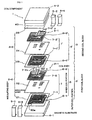
- Fig. 1 is an exploded perspective view of a coil component according to a first embodiment of the present invention.
- Fig. 2 is an external view of the coil component.
- Fig. 3 is a cross-sectional view taken along line A-A in Fig. 2.
- a coil component 1 serves as a common-mode choke coil that is applicable to a high-speed differential transmission line of DVI standard or HDMI standard.
- a coil component 1 includes a first coil block 2 and a second coil block 3 that are sandwiched between a pair of magnetic substrates 4-1, 4-2 so as to form a box-shaped chip body, and four external electrodes 5-1 to 5-4 that are attached to outer surfaces of the chip body.
- the first coil block 2 is provided on the magnetic substrate 4-1 and includes a single coil body 2-1 having an outer coil portion 6 and an inner coil portion 7, and an insulating body 2-2 that encompasses the coil body 2-1.
- the coil body 2-1 is formed such that the inner coil portion 7 is electrically connected to the outer coil portion 6 while being surrounded by the outer coil portion 6.
- the outer coil portion 6 and the inner coil portion 7 include a plurality of patterns that are connected to each other.
- Fig. 4 includes plan views showing a structure of the first coil block 2. In order to provide an easier understanding of the illustration, the patterns included in the outer coil portion 6 are shaded.
- the insulating body 2-2 (see Fig. 1) of the first coil block 2 includes insulating layers 21 to 23 that are stacked one on top of another.
- the outer coil portion 6 and the inner coil portion 7 are pattern-formed on the insulating layers 21 to 23.
- the outer coil portion 6 includes a first pattern group 6-1 disposed on the insulating layer 21 and a second pattern group 6-2 disposed on the insulating layer 22.
- the first pattern group 6-1 includes rectangular annular patterns 61, 62 doubly disposed on the insulating layer 21 and having different diameters, and a first extending portion 60 disposed outside of the annular patterns 61, 62. Furthermore, each annular pattern 61 (62) has opposite end segments 61a, 61b (62a, 62b) that overlap with each other in the vertical direction of the page. While extending along the segments, the first extending portion 60 is bent so as to extend at a left side of a center axis L1. One end segment 60a of the first extending portion 60 is disposed on a lower edge of the insulating layer 21 in the drawing and to the left of the center axis L1. Accordingly, the end segment 60a of the first extending portion 60 is exposed from the first coil block 2.
- the second pattern group 6-2 includes rectangular annular patterns 63, 64, 65 that are triply disposed on the insulating layer 22.
- Each annular pattern 63 (64, 65) has opposite end segments 63a, 63b (64a, 64b, 65a, 65b) that opposed to each other while being separated from each other by a predetermined distance.
- the end segments 63a, 64a, 65a and the end segments 63b, 64b, 65b have a gap B therebetween.
- the end segments 63a, 64a, 65a and the end segments 63b, 64b, 65b are not completely opposed to each other, but are slightly misaligned from each other in the vertical direction of the page.
- the end segments 63a, 64a, 65a are substantially aligned with the respective end segments 60b, 61b, 62b of the first extending portion 60 and the annular patterns 61, 62 included in the first pattern group 6-1.
- the end segments 63b, 64b are substantially aligned with the end segments 61a, 62a, respectively.
- the end segment 65b of the annular pattern 65 is a free end.
- the first and second pattern groups 6-1, 6-2 face each other across the insulating layer 22 and are electrically connected to each other through via holes 22a to 22f provided in the insulating layer 22.
- the end segment 60b of the first extending portion 60 is connected to the free end segment 63a of the outermost annular pattern 63 through the via hole 22a.
- the end segment 63b of the annular pattern 63 is connected to the end segment 61a of the annular pattern 61 through the via hole 22b.
- the end segment 61b of the annular pattern 61 is connected to the end segment 64a of the annular pattern 64 through the via hole 22c.
- the end segment 64b of the annular pattern 64 is connected to the end segment 62a of the annular pattern 62 through the via hole 22d.
- the end segment 62b of the annular pattern 62 is connected to the end segment 65a of the annular pattern 65 through the via hole 22e.
- connection structure for example, the second outermost annular pattern 62 in the first pattern group 6-1 and the second outermost annular pattern 64 in the second pattern group 6-2 are connected helically to each other via the end segments 62a, 64b. Moreover, the other end segment 62b of the second annular pattern 62 and the end segment 65a of the third annular pattern 65 in the second pattern group 6-2 are connected, whereby the second annular pattern 62 and the third annular pattern 65 are helically connected to each other.
- the remaining n-th annular patterns of the first and second pattern groups 6-1, 6-2 are connected helically to each other, and the n-th and (n+1)-th annular patterns of the first and second pattern groups 6-1, 6-2 are also connected helically to each other in the same manner as above.
- the entire outer coil portion 6 having the first and second pattern groups 6-1, 6-2 forms an alternating helix in the vertical direction (i.e. front-back direction of the page).
- the inner coil portion 7 includes a first spiral pattern 7-1 provided on the insulating layer 21 and a second spiral pattern 7-2 provided on the insulating layer 22.
- the first spiral pattern 7-1 has a spiral with a little over two turns and is disposed within the innermost annular pattern 62 of the first pattern group 6-1.
- the first spiral pattern 7-1 has an outer end segment 7-1a that is connected to the free end segment 65b of the innermost annular pattern 65 of the second pattern group 6-2 through the via hole 22f in the insulating layer 22.
- the second spiral pattern 7-2 has a spiral with substantially two turns and is disposed within the innermost annular pattern 65 of the second pattern group 6-2.
- the second spiral pattern 7-2 has an inner end segment 7-2a that is connected to an inner end segment 7-1b of the first spiral pattern 7-1 through a via hole 22g provided in the insulating layer 22.
- the second spiral pattern 7-2 has a second extending portion 7-2b that extends to the left of a center axis L2 through the gap B of the second pattern group 6-2.
- An end segment 7-2c of the second extending portion 7-2b is disposed on an upper edge of the insulating layer 22 in the drawing and to the left of the center axis L2. Accordingly, the end segment 7-2c is exposed from the first coil block 2 at a position opposite to the end segment 60a of the first extending portion 60.
- the insulating layer 23 is stacked on the second pattern group 6-2 and the second spiral pattern 7-2, thereby forming the single coil body 2-1 having the helical-shaped outer coil portion 6 and the spiral-shaped inner coil portion 7. Furthermore, the coil body 2-1 is encompassed by the insulating body 2-2 having the insulating layers 21 to 23, thereby forming the first coil block 2.
- a line length of the outer coil portion 6, or more specifically, a total line length of the first extending portion 60, the annular patterns 61, 62, and the annular patterns 63, 64, 65 is set within a range of 1/2 to 5/6 inclusive of a line length of the coil body 2-1, that is, a total length of the patterns 60 to 65 and the first and second spiral patterns 7-1, 7-2.
- the second coil block 3 has substantially the same structure as the first coil block 2 and includes a single coil body 3-1 having an outer coil portion 6' and an inner coil portion 7', and an insulating body 3-2 that encompasses the coil body 3-1.
- the second coil block 3 is disposed on the first coil block 2 in a manner such that the coil body 3-1 of the second coil block 3 is coaxial with the coil body 2-1 of the first coil block 2.
- the coil body 3-1 has substantially the same structure as the coil body 2-1, a first extending portion and a second extending portion thereof are disposed at different positions from those of the coil body 2-1.
- Fig. 5 includes plan views showing a structure of the second coil block 3. In order to provide an easier understanding of the illustration, the patterns included in the outer coil portion 6' are shaded.
- the coil body 3-1 of the second coil block 3 includes first and second pattern groups 6-1', 6-2' of the outer coil portion 6' and first and second spiral patterns 7-1', 7-2' of the inner coil portion 7', which are pattern-formed on insulating layers 23 to 25 included in the insulating body 3-2.
- the first pattern group 6-1' of the outer coil portion 6' (see Fig. 1) and the first spiral pattern 7-1' of the inner coil portion 7' (see Fig. 1) are pattern-formed on the insulating layer 23.
- the second pattern group 6-2' of the outer coil portion 6' and the second spiral pattern 7-2' of the inner coil portion 7' are pattern-formed on the insulating layer 24.
- the outer coil portion 6' has a structure in which a first extending portion 60' and annular patterns 61, 62 in the first pattern group 6-1' are helically connected to annular patterns 63, 64, 65 in the second pattern group 6-2' through corresponding via holes 24a to 24f provided in the insulating layer 24.
- the inner coil portion 7' has a structure in which the first spiral pattern 7-1' and the second spiral pattern 7-2' are connected to each other in series through a via hole 24g.
- first extending portion 60' extends to the right of a center axis L1' of the insulating layer 23 and has an end segment 60'a which is exposed from the second coil block 3.
- a second extending portion 7-2'b extending through the gap B is bent also to the right of a center axis L2' of the insulating layer 24 and has an end segment 7-2' c which is exposed from the second coil block 3.
- the insulating layer 25 is stacked on the second pattern group 6-2' and the second spiral pattern 7-2', thereby forming the second coil block 3.
- a line length of the outer coil portion 6' is set within a range of 1/2 to 5/6 inclusive of a line length of the coil body 3-1.
- the magnetic substrate 4-2 is adhered to the insulating layer 25 of the second coil block 3 with an adhesive 40, thereby forming a box-shaped chip body.
- the external electrodes 5-1 to 5-4 are attached to outer surfaces of the chip body, such that the external electrodes 5-1, 5-2 are respectively connected to the end segments 60a, 7-2c of the coil body 2-1 and that the external electrodes 5-3, 5-4 are respectively connected to the end segments 60'a, 7-2'c of the coil body 3-1.
- the coil component 1 according to the first embodiment is a laminated wafer that is formed by alternately stacking the first pattern group 6-1 and the first spiral pattern 7-1, the second pattern group 6-2 and the second spiral pattern 7-2, the first pattern group 6-1' and the first spiral pattern 7-1', the second pattern group 6-2' and the second spiral pattern 7-2', and the insulating layers 21 to 25 onto the magnetic substrate 4-1, and then adhering the magnetic substrate 4-2 onto the uppermost layer.
- the following materials are used for each of the layers.
- the magnetic substrates 4-1, 4-2 are used as substrates.
- the magnetic substrate 4-1 is preferably polished so that its surface roughness Ra is 0.5 ⁇ m or less.
- dielectric substrates or insulating substrates may be used depending on the intended usage of the coil component.
- a resin material such as polyimide resin, epoxy resin, and benzocyclobutene resin, a glass material such as SiO 2 , a glass-ceramic material, a dielectric material, or a combination of different materials may be used. Since a photolithography technique is employed in the first embodiment, photosensitive polyimide resin is used as a material for forming the insulating layers 21 to 25.
- a highly conductive metallic material such as Ag, Pd, Cu, and Al, or an alloy of these metallic materials may be used.
- Ag is used.
- the combination between an insulating material and a conductive material is preferably selected in view of, for example, workability and adhesiveness.
- thermosetting polyimide resin is used as the adhesive 40.
- an insulating material is first applied over the magnetic substrate 4-1 and is photo-cured so as to form the insulating layer 21 (first insulating layer). Then, a film composed of a conductive material is formed over the insulating layer 21 by a thin-film formation technique, such as sputtering and vapor deposition, or by a thick-film formation technique, such as screen printing. Subsequently, a photolithography process including a series of steps, such as a resist coating step, an exposure step, a developing step, an etching step, and a resist removal step, is performed so as to form the first pattern group 6-1 and the first spiral pattern 7-1 on the insulating layer 21.
- a thin-film formation technique such as sputtering and vapor deposition
- a thick-film formation technique such as screen printing.
- a photolithography process including a series of steps, such as a resist coating step, an exposure step, a developing step, an etching step, and a resist removal step, is performed so
- the first pattern group 6-1 and the first spiral pattern 7-1 are applied over the first pattern group 6-1 and the first spiral pattern 7-1 so as to form the insulating layer 22 (second insulating layer) provided with the via holes 22a to 22g by means of photolithography.
- a film composed of a conductive material is formed over the insulating layer 22, and then the second pattern group 6-2 and the second spiral pattern 7-2 are formed on the insulating layer 22 by means of photolithography.
- the second pattern group 6-2 and the second spiral pattern 7-2 of the upper layer and the first pattern group 6-1 and the first spiral pattern 7-1 of the lower layer are electrically connected through the via holes 22a to 22g. Accordingly, this forms the first coil block 2 having the coil body 2-1 encompassed by the insulating body 2-2.
- the insulating layers 23 to 25, the first and second pattern groups 6-1', 6-2', and the first and second spiral patterns 7-1', 7-2' are alternately stacked one on top of another, thereby forming the second coil block 3 having the coil body 3-1 encompassed by the insulating body 3-2.
- the magnetic substrate 4-2 having the adhesive 40 applied thereon is adhered to the insulating layer 25 of the second coil block 3.
- a heating-compressing process is performed in a vacuum or in an inert gas, and then a cooling process is performed. After the cooling process, the pressure is released, whereby the magnetic substrate 4-2 becomes tightly joined to the second coil block 3.
- each of the external electrodes 5-1 to 5-4 is formed by first forming a first metallic film by applying a conductive paste containing a material of, for example, AG, Ab-Pd, Cu, NiCr, or NiCu or by sputtering or vapor depositing the material, and then forming a second metallic film composed of, for example, Ni, Sn, or Sn-Pb over the first metallic film by wet electrolytic plating.
- the stray capacitance and the line length can be controlled with high precision, thereby contributing to manufacturing of a high-precision coil component 1.
- Fig. 6 is a schematic diagram showing a state where the coil component 1 is incorporated in a high-speed differential transmission line of DVI standard or HDMI standard.
- a transmitter 400 of a personal computer is connected to a receiver 401 on a monitor side via a cable 402.
- the following description is directed to a case where the coil component 1 is incorporated in a high-speed differential transmission line of DVI standard or HDMI standard that transmits digital differential signals D+, D- from the transmitter 400 to the receiver 401.
- a pair of clock differential signals and three pairs of data differential signals D+, D- are generally transmitted.
- the description below will refer only to a line that transmits one of the pairs of differential signals D+, D- and will therefore be directed to an example in which the coil component 1 is incorporated in this line.
- the coil component 1 functions as a common-mode choke coil. Specifically, in a normal mode, a differential signal D+ is input to the coil body 2-1 through the external electrode 5-1 and is then output from the external electrode 5-2. On the other hand, a differential signal D- of an opposite phase is input to the coil body 3-1 through the external electrode 5-3 and is then output from the external electrode 5-4. In this case, the differential signal D+ input to the coil body 2-1 through the external electrode 5-1 travels helically through the outer coil portion 6 and then travels through the inner coil portion 7 in a rotating fashion so as to reach the external electrode 5-2.
- the differential signal D- input to the coil body 3-1 through the external electrode 5-4 travels through the inner coil portion 7' in a rotating fashion and then travels helically through the outer coil portion 6' so as to reach the external electrode 5-3. Consequently, since the differential signals D+, D- travel in opposite directions, a magnetic field within the coil component 1 shrinks, whereby the impedance in the coil component 1 is reduced. Thus, the differential signals D+, D- are transmitted through the coil component 1 without attenuation.
- the coil component 1 is a multilayer component, and in the coil body 2-1 (3-1), the second pattern group 6-2 and the second spiral pattern 7-2 forming the upper layer and the first pattern group 6-1 and the first spiral pattern 7-1 forming the lower layer (the first and second pattern groups 6-1', 6-2' and the first and second spiral patterns 7-1' , 7-2') face each other. Therefore, stray capacitance generated between these patterns may be of concern. In other words, if the stray capacitance is high, the self-resonance frequency of the coil body 2-1 (3-1) is low, thus lowering the impedance against high frequency noise and significantly deteriorating the noise attenuation effect. In particular, the most problematic stray capacitance is the stray capacitance generated between outer periphery patterns that have large line lengths.
- the coil component 1 operates so as to reduce stray capacitance.
- Fig. 7 is a perspective view of the outer coil portion 6 for illustrating such a stray-capacitance reducing effect.
- stray capacitance C1 generated between a point P1 on the outermost first extending portion 60 in the first pattern group 6-1 and a point P2 on the annular pattern 63 in the second pattern group 6-2, which faces the point P1, is dependent upon a line length between the point P1 and the point P2. Due to the connection between the end segment 60a and the end segment 63a, the outermost first extending portion 60 is helically connected to the annular pattern 63.
- the line length between the point P1 and the point P2 is equal to a sum of a line between the point P1 and the end segment 60b of the first extending portion 60 and a line between the end segment 63a and the point P2 of the annular pattern 63.
- the first embodiment solves this problem by disposing the inner coil portion 7 within the outer coil portion 6 to omit unnecessary overlapping sections so as to achieve high inductance within a small space.
- the outer coil portion 6 with low stray capacitance is disposed in an outer region of the coil body 2-1 to increase the self-resonance frequency
- the inner coil portion 7 that is capable of attaining high inductance is disposed in an inner region of the coil body 2-1, thereby achieving lower stray capacitance and higher inductance in the coil body 2-1.
- the coil component 1 functions as a common-mode choke coil having a high frequency property.
- a fraction of the coil body 2-1 (3-1) occupied by the line length of the outer coil portion 6 (6') is related to the self-resonance frequency of the coil component 1 or to the common-mode impedance.
- Fig. 8 is a graph that shows the relationships among a fraction of a total line length of the coil body 2-1 (3-1) occupied by the line length of the outer coil portion 6 (6'), a self-resonance frequency of the coil component 1, and common-mode impedance in a common mode according to the miniature coil component 1 having a size of 0.8 mm ⁇ 0.6 mm.
- a curve S1 corresponds to a self-resonance frequency curve
- a curve S2 corresponds to a common-mode impedance curve.
- a self-resonance frequency of the coil component 1 increases as the fraction occupied by the outer coil portion 6 (6') increases.
- the impedance in a common mode decreases as the fraction increases.
- the coil component 1 in view of a transmission line in which the coil component 1 is to be incorporated, it is necessary to determine an appropriate fraction occupied by the outer coil portion 6 (6') so that both high self-resonance frequency (low stray capacitance) of the coil component 1 and high impedance (high inductance) in a common mode can be achieved. Since the coil component 1 according to the first embodiment is intended to be incorporated into a high-speed differential transmission line of DVI standard or HDMI standard, a self-resonance frequency of about 580 MHz to 720 MHz and a common-mode impedance of 60 ⁇ or more are desirably attained. Consequently, it is assumable that a fraction occupied by the line length of the outer coil portion 6 (6') is preferably set within a range of 1/2 to 5/6 inclusive of the line length of the coil body 2-1 (3-1).
- the inventors of the present invention measured a frequency characteristic of the coil component 1 in which the fraction occupied by the outer coil portion 6 (6') is set within the above-referenced range and a frequency characteristic of a coil component of a conventional type.
- Fig. 9 is a graph that shows the frequency characteristic of the coil component 1 according to the first embodiment and the frequency characteristic of the coil component of the conventional type.
- the coil component 1 of the first embodiment having a size of 0.8 mm ⁇ 0.6 mm was used, and a fraction occupied by the outer coil portion 6 (6') was set at 7/10.
- a frequency curve F1 having a peak at a frequency of 650 MHz was obtained, as shown in Fig. 9.
- the coil component 1 has a high self-resonance frequency of 650 MHz.
- Fig. 10 includes plan views of a first coil block, which is a relevant portion of a coil component 1' according to the second embodiment of the present invention.
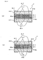
- Fig. 11 includes cross-sectional views illustrating an electromagnetic coupling between coil bodies.
- the second coil block 3 is stacked on the first coil block 2 in a manner such that the pattern unit with the higher density in one coil body is disposed facing the pattern unit with the higher density in the other coil body.
- the density of the pattern unit consisting of the first pattern group 6-1 (6-1') and the first spiral pattern 7-1 (7-1') is higher than the density of the pattern unit consisting of the second pattern group 6-2 (6-2') and the second spiral pattern 7-2 (7-2'). Therefore, in the second embodiment, the pattern unit consisting of the first pattern group 6-1 and the first spiral pattern 7-1 of the coil body 2-1 is disposed facing the pattern unit consisting of the first pattern group 6-1' and the first spiral pattern 7-1' of the coil body 3-1.
- a multilayer structure of the first coil block 2 is an inversion of the multilayer structure of the first coil block in the first embodiment shown in Fig. 4.
- the second pattern group 6-2 and the second spiral pattern 7-2 are formed on the bottommost insulating layer 21. Furthermore, as shown in Figs. 10(b) and 10(c), the first pattern group 6-1 and the first spiral pattern 7-1 are formed on the insulating layer 22. The second pattern group 6-2 and the second spiral pattern 7-2 are electrically connected to the first pattern group 6-1 and the first spiral pattern 7-1 through the corresponding via holes 22a to 22f. Moreover, as shown in Fig. 10(d), the insulating layer 23 is stacked over the first pattern group 6-1 and the first spiral pattern 7-1.
- the higher-density pattern unit consisting of the first pattern group 6-1 and the first spiral pattern 7-1 of the coil body 2-1 is disposed facing the higher-density pattern unit consisting of the first pattern group 6-1' and the first spiral pattern 7-1' of the coil body 3-1, thereby strengthening the electromagnetic coupling between the coil body 2-1 and the coil body 3-1.
- the coil component 1' in the second embodiment when used as a common-mode choke coil, the normal-mode impedance of the coil component 1' can be reduced. Consequently, an insertion loss of a differential signal in a normal mode is reduced, thereby effectively removing only common-mode noise while preventing attenuation of the differential signal.
- the coil component 1 in the first embodiment has the structure as shown in Fig. 11(b) in which the lower-density pattern unit consisting of the second pattern group 6-2 and the second spiral pattern 7-2 of the coil body 2-1 is disposed facing the higher-density pattern unit consisting of the first pattern group 6-1' and the first spiral pattern 7-1' of the coil body 3-1.
- the coil component 1' according to the second embodiment is modified such that the degree of electromagnetic coupling is much higher than that of electromagnetic coupling between the coil bodies 2-1, 3-1 in the coil component 1 according to the first embodiment.
- a fraction occupied by the line length of the outer coil portion 6 (6') of the coil component 1 is set within a range of 1/2 to 5/6 inclusive of the line length of the coil body 2-1 (3-1) in the above embodiments, the fraction is not limited within this range.
- a typical high-speed differential transmission line such as a USB (universal serial bus)
- This can be sufficiently achieved by setting the fraction occupied by the line length of the outer coil portion 6 (6') of the coil component 1 to 1/3 or more of the line length of the coil body 2-1 (3-1).
- first and second coil blocks 2, 3 constitute the coil component 1 in order to allow the coil component 1 to function as a common-mode choke coil in the above embodiments
- the present invention may alternatively include a coil component having a single coil block, as in a ferrite bead.
- magnetic substrates 4-1, 4-2 are included in the above embodiments, this does not mean that a coil component not having these substrates or a coil component having only a single substrate is excluded from the scope of the present invention.
Landscapes
- Engineering & Computer Science (AREA)
- Power Engineering (AREA)
- Microelectronics & Electronic Packaging (AREA)
- Coils Or Transformers For Communication (AREA)
Abstract
Description
- The present invention relates to coil components incorporated in, for example, electronic circuits, and particularly, to a multilayer coil component used in a highfrequency circuit.
- A typical coil component incorporated in an electronic circuit of, for example, a cellular phone is shown in Fig. 12.
- As shown in Fig. 12, a
coil component 100 includes a multi-turnspiral pattern 101 disposed on aninsulating layer 102, and aninsulating layer 103 stacked on thespiral pattern 101. Theinsulating layer 103 has an extendingportion 104 thereon, which is connected to thespiral pattern 101 through avia hole 105. - Improvements in miniaturization and high inductance in coil components are in great demand in compliance with compactness of mobile communication devices, such as cellular phones nowadays. However, with the
coil component 100 having the multi-turnspiral pattern 101 within a single layer, a sufficient number of turns for achieving high inductance cannot be attained in view of limitation of space. - Consequently, there is proposed a technology for attaining a small-size high-inductance coil component by forming multilayer spiral patterns, as shown in Fig. 13.
- A
coil component 200 shown in Fig. 13 is a multilayer type that has twospiral patterns - In detail, the first
spiral pattern 201 is provided on theinsulating layer 102, and the secondspiral pattern 202 is provided on theinsulating layer 103. Central portions of thespiral patterns via hole 105. - In this case, although the multilayer spiral pattern coil provides a sufficient number of turns and high inductance, the
coil component 200 has higher stray capacitance in comparison to thecoil component 100 shown in Fig. 12. In particular, a stray capacitance value produced in an outer periphery portion of the coil is extremely high. - For example, as shown in Fig. 13, a line extending from an outermost periphery point P1 of the
spiral pattern 201 to a point P2 of thespiral pattern 202 corresponding to the point P1 is equal to a sum of a path extending between the point P1 and a central portion 201a of thespiral pattern 201 and a path extending between acentral portion 202a of thespiral pattern 202 and the point P2, meaning that the line is extremely long. Thus, a potential difference between the point P1 and the point P2 is large, and therefore, stray capacitance C200 produced between the point P1 and the point P2 is high. Such an increase in stray capacitance value leads to a decrease in self-resonance frequency of thecoil component 200, thus deteriorating the high frequency property of thecoil component 200. - In contrast, a
multilayer coil component 300 that inhibits an increase in stray capacitance has been proposed, as shown in Fig. 14 (for example, seePatent Document 1 and Patent Document 2). - The
coil component 300 includes apattern group 301 disposed on theinsulating layer 102, and theinsulating layer 103 stacked on thepattern group 301. Thepattern group 301 includes rectangularannular patterns 311 to 316 that have overlapping opposite end segments and that are arranged substantially concentrically on theinsulating layer 102. Thecoil component 300 also includes apattern group 302 having rectangularannular patterns 321 to 326 that are arranged substantially concentrically on theinsulating layer 103. Theannular patterns 321 to 326 have non-overlapping end segments that are separated by a predetermined distance. First ends of theannular patterns 321 to 326 are connected to first ends of theannular patterns 311 to 316 throughcorresponding via holes 105a to 105j provided in theinsulating layer 103. - Accordingly, for example, a line extending from an outermost periphery point P1 of the
pattern group 301 to a point P2 of thepattern group 302 corresponding to the point P1 is equal to a sum of a path extending between the point P1 and an end 311a of theannular pattern 311 and a path extending between anend 321a of theannular pattern 321 and the point P2, meaning that the line is extremely short. Therefore, a potential difference between the point P1 and the point P2 is small, whereby stray capacitance C300 produced between the point P1 and the point P2 is low.
Patent Document 1:Japanese Unexamined Patent Application Publication No. 55-096605
Patent Document 2:Japanese Unexamined Patent Application Publication No. 5-291044 - However, although the stray capacitance can be reduced in the
coil component 300 shown in Fig. 14, a sufficient number of turns for achieving high inductance cannot be attained. - In other words, since the opposite end segments of the
annular patterns 311 to 316 are arrayed in an overlapping manner, each annular pattern requires an area for disposing the corresponding opposite end segments in the arrayed direction of the opposite end segments (i.e. in a front direction closer to the viewer of Fig. 14). Therefore, in view of limitation of space, a sufficient number ofannular patterns 311 to 316 cannot be attained, which implies that thepattern group 301 cannot provide a sufficient number of turns. Consequently, it is difficult to achieve high inductance of thecoil component 300. - It is an object of the present invention to solve the problems mentioned above by providing a coil component in which both low stray capacitance and high inductance are achieved.
- In order to achieve the above-referenced object, the invention of
Claim 1 provides a coil component, which includes at least one coil block having a single coil body encompassed within an insulating body, the single coil body including an inner coil portion and an outer coil portion, the inner coil portion being electrically connected to the outer coil portion while being surrounded by the outer coil portion. The outer coil portion includes a first pattern group and a second pattern group that are disposed facing each other. The first pattern group includes a plurality of annular patterns having different diameters and each having first and second opposite end segments, and also includes a first extending portion disposed outside of the plurality of annular patterns and having a first end segment that is exposed from the at least one coil block. The second pattern group includes a plurality of annular patterns having different diameters and each having first and second opposite end segments. The n-th annular pattern of the first pattern group from the outside thereof is helically connected to the n-th annular pattern of the second pattern group from the outside thereof via the first end segments. The second end segment of the n-th annular pattern of the first pattern group is connected to one of the end segments of the (n+1)-th annular pattern of the second pattern group in a manner such that the n-th and (n+1)-th annular patterns are helically connected to each other. The first extending portion has a second end segment that is connected to a free end segment of the outermost annular pattern of the second pattern group. The inner coil portion includes a first multi-turn spiral pattern and a second multi-turn spiral pattern. The first spiral pattern is disposed within the innermost annular pattern of the first pattern group and has an outer end segment that is connected to a free end segment of the innermost annular pattern of the second pattern group. The second spiral pattern is disposed within the innermost annular pattern of the second pattern group. The second spiral pattern has an inner end segment that is connected to an inner end segment of the first spiral pattern and also has a second extending portion having an outer end segment that is exposed from the at least one coil block. - Accordingly, when an electric current enters the first extending portion of the outer coil portion, the electric current flows into the outermost annular pattern (n=1) of the second pattern group. Subsequently, the electric current flows helically from this annular pattern in the second pattern group to the outermost annular pattern (n=1) of the first pattern group, and then flows helically from this annular pattern to an inner annular pattern (n=2) in the second pattern group. In a similar manner, the electric current helically flows through the annular patterns in the first pattern group and the annular patterns in the second pattern group in an alternating fashion until finally reaching the innermost annular pattern of the second pattern group. The electric current then enters the first spiral pattern of the inner coil portion, which is disposed within the outer coil portion and whose outer end segment is connected to the innermost annular pattern. The electric current flows inward through the first spiral pattern in a rotating fashion so as to enter the second spiral pattern whose inner end segment is connected to the inner end segment of the first spiral pattern. Subsequently, the electric current flows through the second spiral pattern outward in a rotating fashion so as to be output from the second extending portion. In other words, according to this coil component, the electric current flows helically through the outer coil portion and rotationally through the inner coil portion, whereby a magnetic field is generated in response to the rotating electric current. Thus, the coil component functions as an inductor.
- Meanwhile, in a coil component having patterns that are disposed facing each other, stray capacitance generated between the patterns may be of concern. In particular, stray capacitance generated between outer periphery patterns that have large line lengths has a significant effect on a high frequency property of a coil component. In the coil component according to the present invention, however, because the outermost annular pattern (n=1) in the first pattern group of the outer coil portion is helically connected to the opposing outermost annular pattern (n=1) of the second pattern group, a line extending from the outermost annular pattern of the first pattern group to the outermost annular pattern of the second pattern group is extremely short. Thus, a voltage drop caused in the course of reaching the outermost annular pattern of the second pattern group is reduced, whereby a potential difference between the outermost annular pattern of the first pattern group and the outermost annular pattern of the second pattern group is reduced. Such a reduction of potential difference is achieved not only between the outermost annular patterns but also between other opposing annular patterns. As a result, in addition to the reduction of stray capacitance generated between these outermost annular patterns, the stray capacitance generated between all annular patterns included in the first and second pattern groups is reduced, thereby preventing lowering of self-resonance frequency.
- Furthermore, because the inner coil portion including the first and second spiral patterns that are connected in series is disposed within the outer coil portion, the inner coil portion contributes to an attainment of high inductance, which cannot be achieved solely with the outer coil portion.
- Furthermore, according to the invention of
Claim 2, in the coil component set forth inClaim 1, a line length of the outer coil portion is set to 1/3 or more of a line length of the single coil body. - Accordingly, optimal values for both low stray capacitance and high inductance can be attained.
- Furthermore, according to the invention of
Claim 3, in the coil component set forth in one ofClaims - In particular, according to the invention of Claim 4, in the coil component set forth in
Claim 3, the at least one coil block is formed by means of a photolithography technique. - Although there are various layering techniques for forming the coil block, a photolithography technique may be employed for forming the coil block so that the stray capacitance and the line length can be controlled with high precision.
- Furthermore, according to the invention of Claim 5, in the coil component set forth in one of
Claims 3 and 4, the at least one coil block is disposed on a substrate. - Furthermore, according to the invention of
Claim 6, in the coil component set forth in any one ofClaims 1 to 5, the at least one coil block includes a first coil block and a second coil block, the second coil block being stacked on the first coil block in a manner such that the coil body of the second coil block is coaxial with the coil body of the first coil block. - Accordingly, by incorporating the coil component in a high-speed differential transmission line, the coil component can function as a common-mode choke coil. In other words, in a normal mode, a first differential signal travels through the coil body of the first coil block, and a second differential signal in a direction opposite to the first differential signal travels through the coil body of the second coil block. In a common mode, although high frequency noise travels through the first and second coil blocks in the same direction, the noise is attenuated by the high inductance coils in the first and second coil blocks.
- Furthermore, according to the invention of
Claim 7, in the coil component set forth inClaim 6, the first coil block is disposed on a magnetic substrate, and another magnetic substrate is disposed on the second coil block. - Accordingly, this contributes to higher inductance of the coil component.
- Furthermore, according to the invention of Claim 8, in the coil component set forth in one of
Claims - Accordingly, this strengthens an electromagnetic coupling between the coil body of the first coil block and the coil body of the second coil block.
- As described above, the coil component according to the present invention achieves lower stray capacitance, and prevents lowering of self-resonance frequency, whereby a favorable high frequency property is attained. Furthermore, the inner coil portion contributes to an attainment of high inductance, which cannot be achieved solely with the outer coil portion. Therefore, the outer coil portion and the inner coil portion can be set to optimal line lengths, thereby advantageously achieving both low stray capacitance and high inductance.
- In particular, according to the invention of
Claim 2, since the line length of the outer coil portion may be set to 1/3 or more of the line length of the single coil body, low stray capacitance and high inductance can be optimally achieved. - Furthermore, according to the invention of Claim 4, since the coil block may be formed by means of a photolithography technique, the stray capacitance and the line length can be controlled with high precision, whereby low stray capacitance and high inductance can be achieved with even higher precision.
- Furthermore, the invention of
Claim 6 can provide a coil component that achieves low stray capacitance and high inductance and that can function as a common-mode choke coil. - In particular, the invention of
Claim 7 can provide a coil component that can function as an optimal common-mode choke coil for a high-speed differential transmission line of DVI standard or HDMI standard. - In particular, according to the invention of Claim 8, since the electromagnetic coupling between the coil body of the first coil block and the coil body of the second coil block can be strengthened, if the coil component is used as, for example, a common-mode choke coil, the normal-mode impedance thereof can be reduced, whereby an insertion loss of a differential signal in a normal mode can be reduced. Accordingly, the invention can advantageously provide a common-mode choke coil that can effectively remove only common-mode noise while preventing attenuation of a differential signal.
-
- Fig. 1 is an exploded perspective view of a coil component according to a first embodiment of the present invention.
- Fig. 2 is an external view of the coil component.
- Fig. 3 is a cross-sectional view taken along line A-A in Fig. 2.
- Fig. 4 includes plan views showing a structure of a first coil block.
- Fig. 5 includes plan views showing a structure of a second coil block.
- Fig. 6 is a schematic diagram showing a state where the coil component is incorporated in a high-speed differential transmission line of DVI standard or HDMI standard.
- Fig. 7 is a perspective view of an outer coil portion for illustrating a stray-capacitance reducing effect.
- Fig. 8 is a graph that shows relationships among a fraction of a total line length of a coil body occupied by a line length of the outer coil portion, a self-resonance frequency, and common-mode impedance.
- Fig. 9 is a graph that shows a frequency characteristic of the coil component according to the first embodiment and a frequency characteristic of a coil component of a conventional type.
- Fig. 10 includes plan views of a first coil block, which is a relevant portion of a coil component according to a second embodiment of the present invention.
- Fig. 11 includes cross-sectional views illustrating an electromagnetic coupling between coil bodies.
- Fig. 12 is an exploded perspective view of a coil component according to a first conventional example.
- Fig. 13 is an exploded perspective view of a coil component according to a second conventional example.
- Fig. 14 is an exploded perspective view of a coil component according to a third conventional example.
-
- 1, 1'
- coil component
- 2
- first coil block
- 2-1, 3-1
- coil body
- 2-2, 3-2
- insulating body
- 3
- second coil block
- 4-1, 4-2
- magnetic substrate
- 5-1 to 5-4
- external electrode
- 6, 6'
- outer coil portion
- 6-1, 6-1'
- first pattern group
- 6-2, 6-2'
- second pattern group
- 7, 7'
- inner coil portion
- 7-1, 7-1'
- first spiral pattern
- 7-2, 7-2'
- second spiral pattern
- 7-2b
- second extending portion
- 21 to 25
- insulating layer
- 22a to 22g, 24a to 24g
- via hole
- 40
- adhesive
- 60
- first extending portion
- 61 to 65
- annular pattern
- C1
- stray capacitance
- Preferred embodiments of the present invention will now be described with reference to the drawings.
- Fig. 1 is an exploded perspective view of a coil component according to a first embodiment of the present invention. Fig. 2 is an external view of the coil component. Fig. 3 is a cross-sectional view taken along line A-A in Fig. 2.
- The coil component according to the first embodiment serves as a common-mode choke coil that is applicable to a high-speed differential transmission line of DVI standard or HDMI standard. Referring to Figs. 1 and 2, a
coil component 1 includes afirst coil block 2 and asecond coil block 3 that are sandwiched between a pair of magnetic substrates 4-1, 4-2 so as to form a box-shaped chip body, and four external electrodes 5-1 to 5-4 that are attached to outer surfaces of the chip body. - The
first coil block 2 is provided on the magnetic substrate 4-1 and includes a single coil body 2-1 having anouter coil portion 6 and aninner coil portion 7, and an insulating body 2-2 that encompasses the coil body 2-1. - The coil body 2-1 is formed such that the
inner coil portion 7 is electrically connected to theouter coil portion 6 while being surrounded by theouter coil portion 6. Theouter coil portion 6 and theinner coil portion 7 include a plurality of patterns that are connected to each other. - Fig. 4 includes plan views showing a structure of the
first coil block 2. In order to provide an easier understanding of the illustration, the patterns included in theouter coil portion 6 are shaded. - As will be described later, the insulating body 2-2 (see Fig. 1) of the
first coil block 2 includes insulatinglayers 21 to 23 that are stacked one on top of another. Theouter coil portion 6 and theinner coil portion 7 are pattern-formed on the insulatinglayers 21 to 23. - In detail, referring to shaded sections in Figs. 4(a) to 4(c), the
outer coil portion 6 includes a first pattern group 6-1 disposed on the insulatinglayer 21 and a second pattern group 6-2 disposed on the insulatinglayer 22. - As shown in Fig. 4(a), the first pattern group 6-1 includes rectangular
annular patterns layer 21 and having different diameters, and a first extendingportion 60 disposed outside of theannular patterns opposite end segments portion 60 is bent so as to extend at a left side of a center axis L1. Oneend segment 60a of the first extendingportion 60 is disposed on a lower edge of the insulatinglayer 21 in the drawing and to the left of the center axis L1. Accordingly, theend segment 60a of the first extendingportion 60 is exposed from thefirst coil block 2. - Referring to Fig. 4(c), the second pattern group 6-2 includes rectangular
annular patterns layer 22. Each annular pattern 63 (64, 65) hasopposite end segments end segments end segments end segments end segments end segments respective end segments portion 60 and theannular patterns end segments end segments end segment 65b of theannular pattern 65 is a free end. - The first and second pattern groups 6-1, 6-2 face each other across the insulating
layer 22 and are electrically connected to each other through viaholes 22a to 22f provided in the insulatinglayer 22. In detail, theend segment 60b of the first extendingportion 60 is connected to thefree end segment 63a of the outermostannular pattern 63 through the viahole 22a. Theend segment 63b of theannular pattern 63 is connected to theend segment 61a of theannular pattern 61 through the viahole 22b. Theend segment 61b of theannular pattern 61 is connected to theend segment 64a of theannular pattern 64 through the viahole 22c. Theend segment 64b of theannular pattern 64 is connected to theend segment 62a of theannular pattern 62 through the viahole 22d. Theend segment 62b of theannular pattern 62 is connected to theend segment 65a of theannular pattern 65 through the viahole 22e. - According to this connection structure, for example, the second outermost
annular pattern 62 in the first pattern group 6-1 and the second outermostannular pattern 64 in the second pattern group 6-2 are connected helically to each other via theend segments other end segment 62b of the secondannular pattern 62 and theend segment 65a of the thirdannular pattern 65 in the second pattern group 6-2 are connected, whereby the secondannular pattern 62 and the thirdannular pattern 65 are helically connected to each other. Similarly, the remaining n-th annular patterns of the first and second pattern groups 6-1, 6-2 are connected helically to each other, and the n-th and (n+1)-th annular patterns of the first and second pattern groups 6-1, 6-2 are also connected helically to each other in the same manner as above. Thus, the entireouter coil portion 6 having the first and second pattern groups 6-1, 6-2 forms an alternating helix in the vertical direction (i.e. front-back direction of the page). - On the other hand, referring to Figs. 4(a) and 4(c), the
inner coil portion 7 includes a first spiral pattern 7-1 provided on the insulatinglayer 21 and a second spiral pattern 7-2 provided on the insulatinglayer 22. - In detail, the first spiral pattern 7-1 has a spiral with a little over two turns and is disposed within the innermost
annular pattern 62 of the first pattern group 6-1. The first spiral pattern 7-1 has an outer end segment 7-1a that is connected to thefree end segment 65b of the innermostannular pattern 65 of the second pattern group 6-2 through the viahole 22f in the insulatinglayer 22. On the other hand, the second spiral pattern 7-2 has a spiral with substantially two turns and is disposed within the innermostannular pattern 65 of the second pattern group 6-2. The second spiral pattern 7-2 has an inner end segment 7-2a that is connected to an inner end segment 7-1b of the first spiral pattern 7-1 through a viahole 22g provided in the insulatinglayer 22. Moreover, the second spiral pattern 7-2 has a second extending portion 7-2b that extends to the left of a center axis L2 through the gap B of the second pattern group 6-2. An end segment 7-2c of the second extending portion 7-2b is disposed on an upper edge of the insulatinglayer 22 in the drawing and to the left of the center axis L2. Accordingly, the end segment 7-2c is exposed from thefirst coil block 2 at a position opposite to theend segment 60a of the first extendingportion 60. - The insulating
layer 23 is stacked on the second pattern group 6-2 and the second spiral pattern 7-2, thereby forming the single coil body 2-1 having the helical-shapedouter coil portion 6 and the spiral-shapedinner coil portion 7. Furthermore, the coil body 2-1 is encompassed by the insulating body 2-2 having the insulatinglayers 21 to 23, thereby forming thefirst coil block 2. - In the first embodiment, a line length of the
outer coil portion 6, or more specifically, a total line length of the first extendingportion 60, theannular patterns annular patterns patterns 60 to 65 and the first and second spiral patterns 7-1, 7-2. - Referring to Fig. 1, the
second coil block 3 has substantially the same structure as thefirst coil block 2 and includes a single coil body 3-1 having an outer coil portion 6' and an inner coil portion 7', and an insulating body 3-2 that encompasses the coil body 3-1. Thesecond coil block 3 is disposed on thefirst coil block 2 in a manner such that the coil body 3-1 of thesecond coil block 3 is coaxial with the coil body 2-1 of thefirst coil block 2. - Although the coil body 3-1 has substantially the same structure as the coil body 2-1, a first extending portion and a second extending portion thereof are disposed at different positions from those of the coil body 2-1.
- Fig. 5 includes plan views showing a structure of the
second coil block 3. In order to provide an easier understanding of the illustration, the patterns included in the outer coil portion 6' are shaded. - Referring to Fig. 1, the coil body 3-1 of the
second coil block 3 includes first and second pattern groups 6-1', 6-2' of the outer coil portion 6' and first and second spiral patterns 7-1', 7-2' of the inner coil portion 7', which are pattern-formed on insulatinglayers 23 to 25 included in the insulating body 3-2. - Specifically, referring to Fig. 5(a), the first pattern group 6-1' of the outer coil portion 6' (see Fig. 1) and the first spiral pattern 7-1' of the inner coil portion 7' (see Fig. 1) are pattern-formed on the insulating
layer 23. Moreover, referring to Figs. 5(b) and 5(c), the second pattern group 6-2' of the outer coil portion 6' and the second spiral pattern 7-2' of the inner coil portion 7' are pattern-formed on the insulatinglayer 24. - The outer coil portion 6' has a structure in which a first extending portion 60' and
annular patterns annular patterns holes 24a to 24f provided in the insulatinglayer 24. On the other hand, the inner coil portion 7' has a structure in which the first spiral pattern 7-1' and the second spiral pattern 7-2' are connected to each other in series through a viahole 24g. - Furthermore, the first extending portion 60' extends to the right of a center axis L1' of the insulating
layer 23 and has an end segment 60'a which is exposed from thesecond coil block 3. On the other hand, a second extending portion 7-2'b extending through the gap B is bent also to the right of a center axis L2' of the insulatinglayer 24 and has an end segment 7-2' c which is exposed from thesecond coil block 3. - The insulating
layer 25 is stacked on the second pattern group 6-2' and the second spiral pattern 7-2', thereby forming thesecond coil block 3. - In the
second coil block 3, a line length of the outer coil portion 6' is set within a range of 1/2 to 5/6 inclusive of a line length of the coil body 3-1. - Referring to Fig. 1, the magnetic substrate 4-2 is adhered to the insulating
layer 25 of thesecond coil block 3 with an adhesive 40, thereby forming a box-shaped chip body. The external electrodes 5-1 to 5-4 are attached to outer surfaces of the chip body, such that the external electrodes 5-1, 5-2 are respectively connected to theend segments 60a, 7-2c of the coil body 2-1 and that the external electrodes 5-3, 5-4 are respectively connected to the end segments 60'a, 7-2'c of the coil body 3-1. - A manufacturing process of the
coil component 1 will simply be described below with reference to Fig. 1. - The
coil component 1 according to the first embodiment is a laminated wafer that is formed by alternately stacking the first pattern group 6-1 and the first spiral pattern 7-1, the second pattern group 6-2 and the second spiral pattern 7-2, the first pattern group 6-1' and the first spiral pattern 7-1', the second pattern group 6-2' and the second spiral pattern 7-2', and the insulatinglayers 21 to 25 onto the magnetic substrate 4-1, and then adhering the magnetic substrate 4-2 onto the uppermost layer. For each of the layers, the following materials are used. - The magnetic substrates 4-1, 4-2 are used as substrates. In order to allow a subsequent photolithography process to be performed without any difficulty, the magnetic substrate 4-1 is preferably polished so that its surface roughness Ra is 0.5 µm or less. Alternatively, although magnetic substrates are used in the first embodiment, dielectric substrates or insulating substrates may be used depending on the intended usage of the coil component.
- As an insulating material for forming the insulating
layers 21 to 25, a resin material such as polyimide resin, epoxy resin, and benzocyclobutene resin, a glass material such as SiO2, a glass-ceramic material, a dielectric material, or a combination of different materials may be used. Since a photolithography technique is employed in the first embodiment, photosensitive polyimide resin is used as a material for forming the insulatinglayers 21 to 25. - As a conductive material used for forming the first and second pattern groups 6-1, 6-2, 6-1', 6-2' and the first and second spiral patterns 7-1, 7-2, 7-1', 7-2', a highly conductive metallic material such as Ag, Pd, Cu, and Al, or an alloy of these metallic materials may be used. In the first embodiment, Ag is used. The combination between an insulating material and a conductive material is preferably selected in view of, for example, workability and adhesiveness.
- Furthermore, thermosetting polyimide resin is used as the adhesive 40.
- In the manufacturing process of the
coil component 1, an insulating material is first applied over the magnetic substrate 4-1 and is photo-cured so as to form the insulating layer 21 (first insulating layer). Then, a film composed of a conductive material is formed over the insulatinglayer 21 by a thin-film formation technique, such as sputtering and vapor deposition, or by a thick-film formation technique, such as screen printing. Subsequently, a photolithography process including a series of steps, such as a resist coating step, an exposure step, a developing step, an etching step, and a resist removal step, is performed so as to form the first pattern group 6-1 and the first spiral pattern 7-1 on the insulatinglayer 21. Then, an insulating material is applied over the first pattern group 6-1 and the first spiral pattern 7-1 so as to form the insulating layer 22 (second insulating layer) provided with the viaholes 22a to 22g by means of photolithography. Subsequently, a film composed of a conductive material is formed over the insulatinglayer 22, and then the second pattern group 6-2 and the second spiral pattern 7-2 are formed on the insulatinglayer 22 by means of photolithography. Thus, the second pattern group 6-2 and the second spiral pattern 7-2 of the upper layer and the first pattern group 6-1 and the first spiral pattern 7-1 of the lower layer are electrically connected through the viaholes 22a to 22g. Accordingly, this forms thefirst coil block 2 having the coil body 2-1 encompassed by the insulating body 2-2. - In the same manner as described above, the insulating
layers 23 to 25, the first and second pattern groups 6-1', 6-2', and the first and second spiral patterns 7-1', 7-2' are alternately stacked one on top of another, thereby forming thesecond coil block 3 having the coil body 3-1 encompassed by the insulating body 3-2. Subsequently, the magnetic substrate 4-2 having the adhesive 40 applied thereon is adhered to the insulatinglayer 25 of thesecond coil block 3. In this state, a heating-compressing process is performed in a vacuum or in an inert gas, and then a cooling process is performed. After the cooling process, the pressure is released, whereby the magnetic substrate 4-2 becomes tightly joined to thesecond coil block 3. - Subsequently, a wafer obtained as a result of the above-described process is subject to cutting, such as dicing, so as to be split into 0.8 mm × 0.6 mm sized chip bodies. Then, the external electrodes 5-1 to 5-4 are formed on each chip body. In this case, each of the external electrodes 5-1 to 5-4 is formed by first forming a first metallic film by applying a conductive paste containing a material of, for example, AG, Ab-Pd, Cu, NiCr, or NiCu or by sputtering or vapor depositing the material, and then forming a second metallic film composed of, for example, Ni, Sn, or Sn-Pb over the first metallic film by wet electrolytic plating.
- Accordingly, since a photolithography technique is employed in the manufacturing process of the
coil component 1, the stray capacitance and the line length can be controlled with high precision, thereby contributing to manufacturing of a high-precision coil component 1. - An operation and an advantage of the
coil component 1 according to the first embodiment will now be described. - Fig. 6 is a schematic diagram showing a state where the
coil component 1 is incorporated in a high-speed differential transmission line of DVI standard or HDMI standard. - As shown in Fig. 6, a
transmitter 400 of a personal computer is connected to areceiver 401 on a monitor side via acable 402. The following description is directed to a case where thecoil component 1 is incorporated in a high-speed differential transmission line of DVI standard or HDMI standard that transmits digital differential signals D+, D- from thetransmitter 400 to thereceiver 401. In a transmission type of DVI standard or HDMI standard, a pair of clock differential signals and three pairs of data differential signals D+, D- are generally transmitted. However, in order to provide an easier understanding, the description below will refer only to a line that transmits one of the pairs of differential signals D+, D- and will therefore be directed to an example in which thecoil component 1 is incorporated in this line. - In Fig. 6, the
coil component 1 functions as a common-mode choke coil. Specifically, in a normal mode, a differential signal D+ is input to the coil body 2-1 through the external electrode 5-1 and is then output from the external electrode 5-2. On the other hand, a differential signal D- of an opposite phase is input to the coil body 3-1 through the external electrode 5-3 and is then output from the external electrode 5-4. In this case, the differential signal D+ input to the coil body 2-1 through the external electrode 5-1 travels helically through theouter coil portion 6 and then travels through theinner coil portion 7 in a rotating fashion so as to reach the external electrode 5-2. On the other hand, due to being in opposite phase to the differential signal D+, the differential signal D- input to the coil body 3-1 through the external electrode 5-4 travels through the inner coil portion 7' in a rotating fashion and then travels helically through the outer coil portion 6' so as to reach the external electrode 5-3. Consequently, since the differential signals D+, D- travel in opposite directions, a magnetic field within thecoil component 1 shrinks, whereby the impedance in thecoil component 1 is reduced. Thus, the differential signals D+, D- are transmitted through thecoil component 1 without attenuation. - On the other hand, in a common mode, since noise enters the coil bodies 2-1, 3-1 from the same direction, the magnetic field expands, thereby allowing the
coil component 1 to become in a high impedance state. Thus, the noise is attenuated by thecoil component 1. - Referring back to Fig. 1, the
coil component 1 is a multilayer component, and in the coil body 2-1 (3-1), the second pattern group 6-2 and the second spiral pattern 7-2 forming the upper layer and the first pattern group 6-1 and the first spiral pattern 7-1 forming the lower layer (the first and second pattern groups 6-1', 6-2' and the first and second spiral patterns 7-1' , 7-2') face each other. Therefore, stray capacitance generated between these patterns may be of concern. In other words, if the stray capacitance is high, the self-resonance frequency of the coil body 2-1 (3-1) is low, thus lowering the impedance against high frequency noise and significantly deteriorating the noise attenuation effect. In particular, the most problematic stray capacitance is the stray capacitance generated between outer periphery patterns that have large line lengths. - However, the
coil component 1 according to the first embodiment operates so as to reduce stray capacitance. - Fig. 7 is a perspective view of the
outer coil portion 6 for illustrating such a stray-capacitance reducing effect. - As shown in Fig. 7, stray capacitance C1 generated between a point P1 on the outermost first extending
portion 60 in the first pattern group 6-1 and a point P2 on theannular pattern 63 in the second pattern group 6-2, which faces the point P1, is dependent upon a line length between the point P1 and the point P2. Due to the connection between theend segment 60a and theend segment 63a, the outermost first extendingportion 60 is helically connected to theannular pattern 63. Thus, the line length between the point P1 and the point P2 is equal to a sum of a line between the point P1 and theend segment 60b of the first extendingportion 60 and a line between theend segment 63a and the point P2 of theannular pattern 63. This implies that the line length between the point P1 and the point P2 is extremely short. Therefore, a potential difference between the point P1 and the point P2 is small, whereby the stray capacitance C1 is extremely low, that is, total stray capacitance generated in theouter coil portion 6 is very low. However, in theouter coil portion 6, theend segments miniature coil component 1, a sufficient number of turns cannot be attained solely with theouter coil portion 6 in view of limitation of space, which implies that an attainment of sufficient inductance is impossible with only theouter coil portion 6. The first embodiment solves this problem by disposing theinner coil portion 7 within theouter coil portion 6 to omit unnecessary overlapping sections so as to achieve high inductance within a small space. - In other words, as shown in Fig. 1, the
outer coil portion 6 with low stray capacitance is disposed in an outer region of the coil body 2-1 to increase the self-resonance frequency, and theinner coil portion 7 that is capable of attaining high inductance is disposed in an inner region of the coil body 2-1, thereby achieving lower stray capacitance and higher inductance in the coil body 2-1. Such effect and advantage are similarly achieved by the outer coil portion 6' and the inner coil portion 7' of the coil body 3-1. Accordingly, thecoil component 1 functions as a common-mode choke coil having a high frequency property. - In the
coil component 1 having the above-described structure, a fraction of the coil body 2-1 (3-1) occupied by the line length of the outer coil portion 6 (6') is related to the self-resonance frequency of thecoil component 1 or to the common-mode impedance. - Fig. 8 is a graph that shows the relationships among a fraction of a total line length of the coil body 2-1 (3-1) occupied by the line length of the outer coil portion 6 (6'), a self-resonance frequency of the
coil component 1, and common-mode impedance in a common mode according to theminiature coil component 1 having a size of 0.8 mm × 0.6 mm. A curve S1 corresponds to a self-resonance frequency curve, and a curve S2 corresponds to a common-mode impedance curve. - According to the self-resonance frequency curve S1 in Fig. 8, a self-resonance frequency of the
coil component 1 increases as the fraction occupied by the outer coil portion 6 (6') increases. In contrast, as is apparent from the common-mode impedance curve S2, the impedance in a common mode decreases as the fraction increases. - Therefore, in view of a transmission line in which the
coil component 1 is to be incorporated, it is necessary to determine an appropriate fraction occupied by the outer coil portion 6 (6') so that both high self-resonance frequency (low stray capacitance) of thecoil component 1 and high impedance (high inductance) in a common mode can be achieved. Since thecoil component 1 according to the first embodiment is intended to be incorporated into a high-speed differential transmission line of DVI standard or HDMI standard, a self-resonance frequency of about 580 MHz to 720 MHz and a common-mode impedance of 60 Ω or more are desirably attained. Consequently, it is assumable that a fraction occupied by the line length of the outer coil portion 6 (6') is preferably set within a range of 1/2 to 5/6 inclusive of the line length of the coil body 2-1 (3-1). - In this respect, the inventors of the present invention measured a frequency characteristic of the
coil component 1 in which the fraction occupied by the outer coil portion 6 (6') is set within the above-referenced range and a frequency characteristic of a coil component of a conventional type. - Fig. 9 is a graph that shows the frequency characteristic of the
coil component 1 according to the first embodiment and the frequency characteristic of the coil component of the conventional type. - For the measurement of the frequency characteristic, the
coil component 1 of the first embodiment having a size of 0.8 mm × 0.6 mm was used, and a fraction occupied by the outer coil portion 6 (6') was set at 7/10. As a result, a frequency curve F1 having a peak at a frequency of 650 MHz was obtained, as shown in Fig. 9. In other words, it was proven that thecoil component 1 has a high self-resonance frequency of 650 MHz. - In contrast, a frequency characteristic of a coil component in which each coil body 2-1 (3-1) is entirely formed of a spiral pattern, as in the conventional coil component 200 (see Fig. 13), was measured. As a result, a frequency curve F2 was obtained, which shows that the coil component has an extremely low self-resonance frequency of 200 MHz.
- A second embodiment of the present invention will now be described.
- Fig. 10 includes plan views of a first coil block, which is a relevant portion of a coil component 1' according to the second embodiment of the present invention. Fig. 11 includes cross-sectional views illustrating an electromagnetic coupling between coil bodies.
- In the second embodiment, with respect to densities of pattern units consisting of the first pattern groups 6-1 (6-1') and the first spiral patterns 7-1 (7-1') and densities of pattern units consisting of the second pattern groups 6-2 (6-2') and the second spiral patterns 7-2 (7-2') in the coil bodies 2-1 (3-1), the
second coil block 3 is stacked on thefirst coil block 2 in a manner such that the pattern unit with the higher density in one coil body is disposed facing the pattern unit with the higher density in the other coil body. - For example, referring to Fig. 1, the density of the pattern unit consisting of the first pattern group 6-1 (6-1') and the first spiral pattern 7-1 (7-1') is higher than the density of the pattern unit consisting of the second pattern group 6-2 (6-2') and the second spiral pattern 7-2 (7-2'). Therefore, in the second embodiment, the pattern unit consisting of the first pattern group 6-1 and the first spiral pattern 7-1 of the coil body 2-1 is disposed facing the pattern unit consisting of the first pattern group 6-1' and the first spiral pattern 7-1' of the coil body 3-1.
- In detail, referring to Fig. 10, a multilayer structure of the
first coil block 2 is an inversion of the multilayer structure of the first coil block in the first embodiment shown in Fig. 4. - In other words, as shown in Fig. 10(a), the second pattern group 6-2 and the second spiral pattern 7-2 are formed on the bottommost insulating
layer 21. Furthermore, as shown in Figs. 10(b) and 10(c), the first pattern group 6-1 and the first spiral pattern 7-1 are formed on the insulatinglayer 22. The second pattern group 6-2 and the second spiral pattern 7-2 are electrically connected to the first pattern group 6-1 and the first spiral pattern 7-1 through the corresponding viaholes 22a to 22f. Moreover, as shown in Fig. 10(d), the insulatinglayer 23 is stacked over the first pattern group 6-1 and the first spiral pattern 7-1. - Accordingly, as shown in Fig. 11(a), the higher-density pattern unit consisting of the first pattern group 6-1 and the first spiral pattern 7-1 of the coil body 2-1 is disposed facing the higher-density pattern unit consisting of the first pattern group 6-1' and the first spiral pattern 7-1' of the coil body 3-1, thereby strengthening the electromagnetic coupling between the coil body 2-1 and the coil body 3-1.
- As a result, when the coil component 1' in the second embodiment is used as a common-mode choke coil, the normal-mode impedance of the coil component 1' can be reduced. Consequently, an insertion loss of a differential signal in a normal mode is reduced, thereby effectively removing only common-mode noise while preventing attenuation of the differential signal.
- In contrast, the
coil component 1 in the first embodiment has the structure as shown in Fig. 11(b) in which the lower-density pattern unit consisting of the second pattern group 6-2 and the second spiral pattern 7-2 of the coil body 2-1 is disposed facing the higher-density pattern unit consisting of the first pattern group 6-1' and the first spiral pattern 7-1' of the coil body 3-1. In other words, the coil component 1' according to the second embodiment is modified such that the degree of electromagnetic coupling is much higher than that of electromagnetic coupling between the coil bodies 2-1, 3-1 in thecoil component 1 according to the first embodiment. - Other configurations, operations and advantages in the second embodiment are the same as those in the first embodiment, and therefore will not be described here.
- The technical scope of the present invention is not limited to the above embodiments, and modifications are permissible within the scope and spirit of the present invention.
- For example, although a fraction occupied by the line length of the outer coil portion 6 (6') of the
coil component 1 is set within a range of 1/2 to 5/6 inclusive of the line length of the coil body 2-1 (3-1) in the above embodiments, the fraction is not limited within this range. In other words, in a typical high-speed differential transmission line, such as a USB (universal serial bus), it is satisfactory as long as noise mainly within a range of 200 MHz to 500 MHz can be effectively attenuated. This can be sufficiently achieved by setting the fraction occupied by the line length of the outer coil portion 6 (6') of thecoil component 1 to 1/3 or more of the line length of the coil body 2-1 (3-1). - Furthermore, although the first and second coil blocks 2, 3 constitute the
coil component 1 in order to allow thecoil component 1 to function as a common-mode choke coil in the above embodiments, the present invention may alternatively include a coil component having a single coil block, as in a ferrite bead. - Furthermore, although the magnetic substrates 4-1, 4-2 are included in the above embodiments, this does not mean that a coil component not having these substrates or a coil component having only a single substrate is excluded from the scope of the present invention.
Claims (8)
- A coil component comprising at least one coil block having a single coil body encompassed within an insulating body, the single coil body including an inner coil portion and an outer coil portion, the inner coil portion being electrically connected to the outer coil portion while being surrounded by the outer coil portion,
wherein the outer coil portion includes a first pattern group and a second pattern group that are disposed facing each other, the first pattern group including a plurality of annular patterns having different diameters and each having first and second opposite end segments, and also including a first extending portion disposed outside of the plurality of annular patterns and having a first end segment that is exposed from said at least one coil block, the second pattern group including a plurality of annular patterns having different diameters and each having first and second opposite end segments, wherein the n-th annular pattern of the first pattern group from the outside thereof is helically connected to the n-th annular pattern of the second pattern group from the outside thereof via the first end segments, wherein the second end segment of the n-th annular pattern of the first pattern group is connected to one of the end segments of the (n+1)-th annular pattern of the second pattern group in a manner such that the n-th and (n+1)-th annular patterns are helically connected to each other, and wherein the first extending portion has a second end segment that is connected to a free end segment of the outermost annular pattern of the second pattern group, and
wherein the inner coil portion includes a first multi-turn spiral pattern and a second multi-turn spiral pattern, the first spiral pattern being disposed within the innermost annular pattern of the first pattern group and having an outer end segment that is connected to a free end segment of the innermost annular pattern of the second pattern group, the second spiral pattern being disposed within the innermost annular pattern of the second pattern group, the second spiral pattern having an inner end segment that is connected to an inner end segment of the first spiral pattern and also having a second extending portion having an outer end segment that is exposed from said at least one coil block. - The coil component according to Claim 1, wherein a line length of the outer coil portion is set to 1/3 or more of a line length of the single coil body.
- The coil component according to one of Claims 1 and 2, wherein said at least one coil block has a multilayer structure including a first insulating layer on which the first pattern group and the first spiral pattern are disposed, and a second insulating layer stacked on the first pattern group and the first spiral pattern, the second insulating layer having the second pattern group and the second spiral pattern disposed thereon, wherein the second insulating layer includes a plurality of via holes through which the end segments of the annular patterns in the first pattern group are connected to the corresponding end segments of the annular patterns in the second pattern group, through which the outer end segment of the first spiral pattern is connected to the free end segment of the innermost annular pattern of the second pattern group, and through which the inner end segment of the second spiral pattern is connected to the inner end segment of the first spiral pattern.
- The coil component according to Claim 3, wherein said at least one coil block is formed by means of a photolithography technique.
- The coil component according to one of Claims 3 and 4, wherein said at least one coil block is disposed on a substrate.
- The coil component according to any one of Claims 1 to 5, wherein said at least one coil block comprises a first coil block and a second coil block, the second coil block being stacked on the first coil block in a manner such that the coil body of the second coil block is coaxial with the coil body of the first coil block.
- The coil component according to Claim 6, wherein the first coil block is disposed on a magnetic substrate, and another magnetic substrate is disposed on the second coil block.
- The coil component according to one of Claims 6 and 7, wherein the first pattern group and the first spiral pattern define a pattern unit in the coil body of each of the first and second coil blocks, and the second pattern group and the second spiral pattern define another pattern unit in the coil body of each of the first and second coil blocks, and wherein the second coil block is stacked on the first coil block in a manner such that one of the pattern units with a higher density in the second coil block is disposed facing one of the pattern units with a higher density in the first coil block.
Applications Claiming Priority (3)
| Application Number | Priority Date | Filing Date | Title |
|---|---|---|---|
| JP2004340140 | 2004-11-25 | ||
| JP2005175112 | 2005-06-15 | ||
| PCT/JP2005/018950 WO2006057115A1 (en) | 2004-11-25 | 2005-10-14 | Coil component |
Publications (2)
| Publication Number | Publication Date |
|---|---|
| EP1816658A1 true EP1816658A1 (en) | 2007-08-08 |
| EP1816658A4 EP1816658A4 (en) | 2010-10-20 |
Family
ID=36497858
Family Applications (1)
| Application Number | Title | Priority Date | Filing Date |
|---|---|---|---|
| EP05793092A Withdrawn EP1816658A4 (en) | 2004-11-25 | 2005-10-14 | Coil component |
Country Status (7)
| Country | Link |
|---|---|
| US (1) | US7369028B2 (en) |
| EP (1) | EP1816658A4 (en) |
| JP (1) | JP4381417B2 (en) |
| KR (1) | KR100863889B1 (en) |
| CN (1) | CN101061556B (en) |
| TW (1) | TW200620337A (en) |
| WO (1) | WO2006057115A1 (en) |
Cited By (2)
| Publication number | Priority date | Publication date | Assignee | Title |
|---|---|---|---|---|
| EP2007009A3 (en) * | 2007-06-15 | 2009-12-02 | City University of Hong Kong | Planar emi filter |
| EP2750148A4 (en) * | 2011-08-26 | 2015-06-03 | Rohm Co Ltd | MAGNETIC METAL SUBSTRATE AND INDUCTANCE ELEMENT |
Families Citing this family (46)
| Publication number | Priority date | Publication date | Assignee | Title |
|---|---|---|---|---|
| USD568836S1 (en) * | 2005-04-13 | 2008-05-13 | Nitto Denko Corporation | Groove formed around a semiconductor device on a circuit board |
| USD568838S1 (en) * | 2006-05-01 | 2008-05-13 | Nitto Denko Corporation | Grooves formed around a semiconductor device on a circuit board |
| USD567774S1 (en) * | 2006-05-01 | 2008-04-29 | Nitto Denko Corporation | Groove formed around a semiconductor device on a circuit board |
| WO2007138800A1 (en) * | 2006-06-01 | 2007-12-06 | Murata Manufacturing Co., Ltd. | Layered type balloon transformer |
| US7579824B2 (en) * | 2006-09-29 | 2009-08-25 | Gm Global Technology Operations, Inc. | High-precision Rogowski current transformer |
| US8120445B2 (en) | 2007-06-15 | 2012-02-21 | City University Of Hong Kong | Planar EMI filter comprising coreless spiral planar windings |
| WO2009057421A1 (en) * | 2007-10-30 | 2009-05-07 | Murata Manufacturing Co., Ltd. | Coil part |
| US8056819B2 (en) * | 2008-10-14 | 2011-11-15 | Hong Kong Applied Science And Technology Research Institute Co., Ltd. | Miniature and multi-band RF coil design |
| JP5131260B2 (en) | 2009-09-29 | 2013-01-30 | 株式会社村田製作所 | Multilayer coil device |
| TWI611439B (en) * | 2010-07-23 | 2018-01-11 | 乾坤科技股份有限公司 | Coil device |
| ITTO20110295A1 (en) * | 2011-04-01 | 2012-10-02 | St Microelectronics Srl | INDUCTOR INTEGRATED DEVICE WITH HIGH INDUCTANCE VALUE, IN PARTICULAR FOR USE AS AN ANTENNA IN A RADIOFREQUENCY IDENTIFICATION SYSTEM |
| KR20130017598A (en) * | 2011-08-11 | 2013-02-20 | 삼성전기주식회사 | Coil device and manufacturing method thereof |
| KR101528713B1 (en) * | 2011-08-31 | 2015-06-16 | 가부시키가이샤 무라타 세이사쿠쇼 | Electronic component and method for manufacturing same |
| WO2013094209A1 (en) * | 2011-12-22 | 2013-06-27 | パナソニック株式会社 | Coil component |
| JP5835355B2 (en) | 2012-01-20 | 2015-12-24 | 株式会社村田製作所 | Coil parts |
| US20130271251A1 (en) * | 2012-04-12 | 2013-10-17 | Cyntec Co., Ltd. | Substrate-Less Electronic Component |
| KR101771733B1 (en) * | 2012-08-29 | 2017-08-25 | 삼성전기주식회사 | ESD Protection Pattern Built-in Common Mode Filter |
| US8836460B2 (en) * | 2012-10-18 | 2014-09-16 | International Business Machines Corporation | Folded conical inductor |
| KR20140083577A (en) * | 2012-12-26 | 2014-07-04 | 삼성전기주식회사 | Common mode filter and method of manufacturing the same |
| KR20140094324A (en) * | 2013-01-22 | 2014-07-30 | 삼성전기주식회사 | Common mode filter and method of manufacturing the same |
| KR101975478B1 (en) * | 2013-10-04 | 2019-05-07 | 삼성전기주식회사 | Magnetic substrate and method manufacturing the same, and bonding structure between the magnetic substrate and insulating material, and chip component with the bonding structure |
| US20160012956A1 (en) * | 2014-07-11 | 2016-01-14 | Samsung Electro-Mechanics Co., Ltd. | Thin-type common mode filter and manufacturing method thereof |
| DE102014221568A1 (en) * | 2014-10-23 | 2016-04-28 | Siemens Aktiengesellschaft | Transformer and method for operating a transformer |
| KR102105394B1 (en) * | 2015-03-09 | 2020-04-28 | 삼성전기주식회사 | Coil component and and board for mounting the same |
| KR20170003199A (en) * | 2015-06-30 | 2017-01-09 | 삼성전기주식회사 | Thin film type coil component and method of manufacturing the same |
| CN106531410B (en) * | 2015-09-15 | 2019-08-27 | 臻绚电子科技(上海)有限公司 | Coil, inductance element and method for preparing coil applied to inductance element |
| JP6418134B2 (en) * | 2015-11-02 | 2018-11-07 | 株式会社村田製作所 | Electronic components |
| KR101762023B1 (en) * | 2015-11-19 | 2017-08-04 | 삼성전기주식회사 | Coil component and and board for mounting the same |
| KR101862450B1 (en) | 2016-01-07 | 2018-05-29 | 삼성전기주식회사 | Coil substrate |
| KR101832602B1 (en) * | 2016-03-31 | 2018-02-26 | 삼성전기주식회사 | Common mode filter |
| KR101942730B1 (en) * | 2017-02-20 | 2019-01-28 | 삼성전기 주식회사 | Coil electronic component |
| JP6828555B2 (en) | 2017-03-29 | 2021-02-10 | Tdk株式会社 | Coil parts and their manufacturing methods |
| CN107123540B (en) * | 2017-04-26 | 2018-06-29 | 贵阳顺络迅达电子有限公司 | A kind of manufacturing method of miniature lamination chip component |
| JP6696483B2 (en) * | 2017-07-10 | 2020-05-20 | 株式会社村田製作所 | Coil parts |
| JP7172113B2 (en) * | 2018-04-24 | 2022-11-16 | Tdk株式会社 | Coil component and its manufacturing method |
| JP7092070B2 (en) * | 2019-03-04 | 2022-06-28 | 株式会社村田製作所 | Laminated coil parts |
| JP7200958B2 (en) | 2020-02-04 | 2023-01-10 | 株式会社村田製作所 | common mode choke coil |
| JP7200957B2 (en) | 2020-02-04 | 2023-01-10 | 株式会社村田製作所 | common mode choke coil |
| JP7163935B2 (en) | 2020-02-04 | 2022-11-01 | 株式会社村田製作所 | common mode choke coil |
| JP7200959B2 (en) | 2020-02-04 | 2023-01-10 | 株式会社村田製作所 | common mode choke coil |
| JP7264078B2 (en) | 2020-02-04 | 2023-04-25 | 株式会社村田製作所 | common mode choke coil |
| JP7264127B2 (en) | 2020-08-05 | 2023-04-25 | 株式会社村田製作所 | common mode choke coil |
| JP7322833B2 (en) * | 2020-08-05 | 2023-08-08 | 株式会社村田製作所 | common mode choke coil |
| JP7435351B2 (en) | 2020-08-05 | 2024-02-21 | 株式会社村田製作所 | common mode choke coil |
| JP7211576B1 (en) * | 2021-08-30 | 2023-01-24 | 株式会社村田製作所 | Coil elements, antenna devices, and electronic devices |
| US20250098185A1 (en) * | 2023-09-20 | 2025-03-20 | Apple Inc. | Electronic Device with Three-Dimensional On-Chip Inductors |
Family Cites Families (20)
| Publication number | Priority date | Publication date | Assignee | Title |
|---|---|---|---|---|
| US3785046A (en) * | 1970-03-06 | 1974-01-15 | Hull Corp | Thin film coils and method and apparatus for making the same |
| NL7900244A (en) | 1979-01-12 | 1980-07-15 | Philips Nv | FLAT TWO-LAYER ELECTRICAL COIL. |
| NL7900245A (en) * | 1979-01-12 | 1980-07-15 | Philips Nv | TWO-LAYER FLAT ELECTRICAL COIL WITH BRANCH. |
| DE4117878C2 (en) * | 1990-05-31 | 1996-09-26 | Toshiba Kawasaki Kk | Planar magnetic element |
| JPH05291044A (en) | 1992-04-13 | 1993-11-05 | Murata Mfg Co Ltd | Laminated coil |
| JP2897091B2 (en) * | 1992-07-09 | 1999-05-31 | 株式会社村田製作所 | Line transformer |
| JPH09129458A (en) | 1995-10-30 | 1997-05-16 | Matsushita Electric Ind Co Ltd | Coil parts |
| JPH104015A (en) | 1996-06-17 | 1998-01-06 | Matsushita Electric Ind Co Ltd | Electronic components |
| US6690165B1 (en) * | 1999-04-28 | 2004-02-10 | Hironori Takahashi | Magnetic-field sensing coil embedded in ceramic for measuring ambient magnetic field |
| US6429504B1 (en) * | 2000-05-16 | 2002-08-06 | Tyco Electronics Corporation | Multilayer spiral inductor and integrated circuits incorporating the same |
| JP2002131330A (en) | 2000-10-20 | 2002-05-09 | Matsushita Electric Ind Co Ltd | Acceleration sensor |
| JP2002151330A (en) * | 2000-11-09 | 2002-05-24 | Alps Electric Co Ltd | Spiral inductor |
| JP3791406B2 (en) * | 2001-01-19 | 2006-06-28 | 株式会社村田製作所 | Multilayer impedance element |
| TW578170B (en) * | 2001-01-31 | 2004-03-01 | Endpoints Technology Corp | Inductor apparatus |
| JP4214700B2 (en) * | 2002-01-22 | 2009-01-28 | 株式会社村田製作所 | Common mode choke coil array |
| JP2003217933A (en) | 2002-01-24 | 2003-07-31 | Mitsubishi Materials Corp | LC composite parts |
| JP2004095860A (en) * | 2002-08-30 | 2004-03-25 | Murata Mfg Co Ltd | Laminated coil component and manufacturing method thereof |
| JP2004311828A (en) | 2003-04-09 | 2004-11-04 | Mitsubishi Materials Corp | Laminated common mode choke coil and method of manufacturing the same |
| JP2004339016A (en) | 2003-05-16 | 2004-12-02 | Matsushita Electric Ind Co Ltd | Non-magnetic ferrite and multilayer electronic component using the same |
| JP4339777B2 (en) * | 2004-11-10 | 2009-10-07 | Tdk株式会社 | Common mode choke coil |
-
2005
- 2005-10-14 KR KR1020077011278A patent/KR100863889B1/en not_active Expired - Lifetime
- 2005-10-14 JP JP2006519693A patent/JP4381417B2/en not_active Expired - Lifetime
- 2005-10-14 CN CN2005800398215A patent/CN101061556B/en not_active Expired - Lifetime
- 2005-10-14 EP EP05793092A patent/EP1816658A4/en not_active Withdrawn
- 2005-10-14 WO PCT/JP2005/018950 patent/WO2006057115A1/en not_active Ceased
- 2005-10-24 TW TW094137122A patent/TW200620337A/en not_active IP Right Cessation
-
2007
- 2007-05-02 US US11/743,271 patent/US7369028B2/en not_active Expired - Lifetime
Cited By (2)
| Publication number | Priority date | Publication date | Assignee | Title |
|---|---|---|---|---|
| EP2007009A3 (en) * | 2007-06-15 | 2009-12-02 | City University of Hong Kong | Planar emi filter |
| EP2750148A4 (en) * | 2011-08-26 | 2015-06-03 | Rohm Co Ltd | MAGNETIC METAL SUBSTRATE AND INDUCTANCE ELEMENT |
Also Published As
| Publication number | Publication date |
|---|---|
| US20070205856A1 (en) | 2007-09-06 |
| EP1816658A4 (en) | 2010-10-20 |
| WO2006057115A1 (en) | 2006-06-01 |
| JP4381417B2 (en) | 2009-12-09 |
| CN101061556A (en) | 2007-10-24 |
| TW200620337A (en) | 2006-06-16 |
| JPWO2006057115A1 (en) | 2008-06-05 |
| CN101061556B (en) | 2012-05-09 |
| TWI300574B (en) | 2008-09-01 |
| KR100863889B1 (en) | 2008-10-15 |
| KR20070069208A (en) | 2007-07-02 |
| US7369028B2 (en) | 2008-05-06 |
Similar Documents
| Publication | Publication Date | Title |
|---|---|---|
| EP1816658A1 (en) | Coil component | |
| JP6678292B2 (en) | Common mode noise filter | |
| US6998951B2 (en) | Common mode choke coil array | |
| US8907757B2 (en) | Common mode choke coil and high-frequency electronic device | |
| CN102479601B (en) | Electronic component | |
| US20120313729A1 (en) | Lc composite component and structure for mounting lc composite component | |
| WO2013108862A1 (en) | Coil component | |
| JP5961813B2 (en) | Common mode noise filter | |
| CN108369849B (en) | Common mode noise filter | |
| JP6360174B2 (en) | 3D wire bond type inductor | |
| JP5232562B2 (en) | Multilayer electronic components | |
| JP6977742B2 (en) | Composite electronic components and circuits | |
| CN110415940A (en) | Integrated transformer and electronics | |
| JP2007181169A (en) | Common mode filter | |
| JP4033852B2 (en) | Common mode filter | |
| JP7378015B2 (en) | common mode noise filter | |
| JP4802662B2 (en) | Noise filter | |
| CN100566148C (en) | noise filter | |
| JP7651698B2 (en) | Common Mode Filters and Terminal Devices | |
| KR20210144031A (en) | Coil component | |
| KR101558132B1 (en) | Thin film type coil component and fabricating method thereof | |
| JP2007281315A (en) | Coil component | |
| JPH1051257A (en) | LC low pass filter | |
| JP2019083325A (en) | Common mode choke coil | |
| JP4336319B2 (en) | Multilayer stripline filter |
Legal Events
| Date | Code | Title | Description |
|---|---|---|---|
| PUAI | Public reference made under article 153(3) epc to a published international application that has entered the european phase |
Free format text: ORIGINAL CODE: 0009012 |
|
| 17P | Request for examination filed |
Effective date: 20070329 |
|
| AK | Designated contracting states |
Kind code of ref document: A1 Designated state(s): AT BE BG CH CY CZ DE DK EE ES FI FR GB GR HU IE IS IT LI LT LU LV MC NL PL PT RO SE SI SK TR |
|
| DAX | Request for extension of the european patent (deleted) | ||
| A4 | Supplementary search report drawn up and despatched |
Effective date: 20100922 |
|
| 17Q | First examination report despatched |
Effective date: 20140416 |
|
| GRAP | Despatch of communication of intention to grant a patent |
Free format text: ORIGINAL CODE: EPIDOSNIGR1 |
|
| RIC1 | Information provided on ipc code assigned before grant |
Ipc: H01F 27/34 20060101ALI20140905BHEP Ipc: H01F 27/32 20060101ALI20140905BHEP Ipc: H01F 17/00 20060101AFI20140905BHEP |
|
| INTG | Intention to grant announced |
Effective date: 20140923 |
|
| STAA | Information on the status of an ep patent application or granted ep patent |
Free format text: STATUS: THE APPLICATION IS DEEMED TO BE WITHDRAWN |
|
| 18D | Application deemed to be withdrawn |
Effective date: 20150204 |