EP1814147A1 - Lighting apparatus, exposure apparatus and micro device manufacturing method - Google Patents
Lighting apparatus, exposure apparatus and micro device manufacturing method Download PDFInfo
- Publication number
- EP1814147A1 EP1814147A1 EP05807103A EP05807103A EP1814147A1 EP 1814147 A1 EP1814147 A1 EP 1814147A1 EP 05807103 A EP05807103 A EP 05807103A EP 05807103 A EP05807103 A EP 05807103A EP 1814147 A1 EP1814147 A1 EP 1814147A1
- Authority
- EP
- European Patent Office
- Prior art keywords
- optical system
- emission
- type
- eye
- reflection
- Prior art date
- Legal status (The legal status is an assumption and is not a legal conclusion. Google has not performed a legal analysis and makes no representation as to the accuracy of the status listed.)
- Withdrawn
Links
Images




Classifications
-
- G—PHYSICS
- G03—PHOTOGRAPHY; CINEMATOGRAPHY; ANALOGOUS TECHNIQUES USING WAVES OTHER THAN OPTICAL WAVES; ELECTROGRAPHY; HOLOGRAPHY
- G03F—PHOTOMECHANICAL PRODUCTION OF TEXTURED OR PATTERNED SURFACES, e.g. FOR PRINTING, FOR PROCESSING OF SEMICONDUCTOR DEVICES; MATERIALS THEREFOR; ORIGINALS THEREFOR; APPARATUS SPECIALLY ADAPTED THEREFOR
- G03F7/00—Photomechanical, e.g. photolithographic, production of textured or patterned surfaces, e.g. printing surfaces; Materials therefor, e.g. comprising photoresists; Apparatus specially adapted therefor
- G03F7/70—Microphotolithographic exposure; Apparatus therefor
- G03F7/70058—Mask illumination systems
- G03F7/70075—Homogenization of illumination intensity in the mask plane by using an integrator, e.g. fly's eye lens, facet mirror or glass rod, by using a diffusing optical element or by beam deflection
-
- G—PHYSICS
- G02—OPTICS
- G02B—OPTICAL ELEMENTS, SYSTEMS OR APPARATUS
- G02B27/00—Optical systems or apparatus not provided for by any of the groups G02B1/00 - G02B26/00, G02B30/00
- G02B27/09—Beam shaping, e.g. changing the cross-sectional area, not otherwise provided for
- G02B27/0905—Dividing and/or superposing multiple light beams
-
- G—PHYSICS
- G02—OPTICS
- G02B—OPTICAL ELEMENTS, SYSTEMS OR APPARATUS
- G02B27/00—Optical systems or apparatus not provided for by any of the groups G02B1/00 - G02B26/00, G02B30/00
- G02B27/09—Beam shaping, e.g. changing the cross-sectional area, not otherwise provided for
- G02B27/0938—Using specific optical elements
- G02B27/0977—Reflective elements
- G02B27/0983—Reflective elements being curved
-
- G—PHYSICS
- G03—PHOTOGRAPHY; CINEMATOGRAPHY; ANALOGOUS TECHNIQUES USING WAVES OTHER THAN OPTICAL WAVES; ELECTROGRAPHY; HOLOGRAPHY
- G03F—PHOTOMECHANICAL PRODUCTION OF TEXTURED OR PATTERNED SURFACES, e.g. FOR PRINTING, FOR PROCESSING OF SEMICONDUCTOR DEVICES; MATERIALS THEREFOR; ORIGINALS THEREFOR; APPARATUS SPECIALLY ADAPTED THEREFOR
- G03F7/00—Photomechanical, e.g. photolithographic, production of textured or patterned surfaces, e.g. printing surfaces; Materials therefor, e.g. comprising photoresists; Apparatus specially adapted therefor
- G03F7/70—Microphotolithographic exposure; Apparatus therefor
- G03F7/70058—Mask illumination systems
- G03F7/70091—Illumination settings, i.e. intensity distribution in the pupil plane or angular distribution in the field plane; On-axis or off-axis settings, e.g. annular, dipole or quadrupole settings; Partial coherence control, i.e. sigma or numerical aperture [NA]
-
- G—PHYSICS
- G03—PHOTOGRAPHY; CINEMATOGRAPHY; ANALOGOUS TECHNIQUES USING WAVES OTHER THAN OPTICAL WAVES; ELECTROGRAPHY; HOLOGRAPHY
- G03F—PHOTOMECHANICAL PRODUCTION OF TEXTURED OR PATTERNED SURFACES, e.g. FOR PRINTING, FOR PROCESSING OF SEMICONDUCTOR DEVICES; MATERIALS THEREFOR; ORIGINALS THEREFOR; APPARATUS SPECIALLY ADAPTED THEREFOR
- G03F7/00—Photomechanical, e.g. photolithographic, production of textured or patterned surfaces, e.g. printing surfaces; Materials therefor, e.g. comprising photoresists; Apparatus specially adapted therefor
- G03F7/70—Microphotolithographic exposure; Apparatus therefor
- G03F7/70058—Mask illumination systems
- G03F7/702—Reflective illumination, i.e. reflective optical elements other than folding mirrors, e.g. extreme ultraviolet [EUV] illumination systems
Definitions
- This invention pertains to illumination apparatuses for manufacturing microdevices such as semiconductor devices, liquid-crystal-display devices, thin-film magnetic heads and the like in lithographic processes, exposure apparatus comprising the illumination apparatuses.
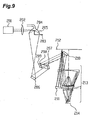
- An exposure apparatus as noted above is exemplified by the prior-art system shown in FIG. 9.
- a target material supplied by a nozzle 203, is irradiated at a point 204 with laser light emitted from a non-EUV laser-light source 201 and condensed by a condensing element 202.
- the target material receives an intensely concentrated dose of energy that converts the target material into a plasma that generates EUV light.
- the generated EUV light is condensed by a condensing mirror 205 and reflected by a concave mirror 206.
- the EUV light then is incident on an incidence-side fly-eye mirror 207, in which numerous concave mirror segments are arranged in rows.
- the beam reflected by the incidence-side fly-eye mirror 207 passes through a diaphragm aperture 208 and is reflected by an emission-side fly-eye mirror 209, in which numerous concave mirror segments are arranged in rows.
- the beam again passes through the diaphragm aperture 208 and is incident on an optical assembly 210.
- the beam reflected by the optical assembly 210 is condensed by a condensing optical assembly 211 for irradiation of a mask 212.
- the beam carries an image of the pattern defined on the irradiated mask 212 as the beam passes through a projection-optical system 213, which projects the image onto a wafer (photosensitive substrate) 214.
- the incidence-side fly-eye mirror 207 and the emission-side fly-eye mirror 208 are separated from each other by a short distance. Consequently, the incidence angle of the beam on the incidence-side fly-eye mirror 207 is large.
- the distance between the incidence-side fly-eye mirror 207 and the emission-side fly-eye mirror 209 must be increased. To accommodate this greater distance, the focal length of the condensing optical assembly 211 would have to be increased.
- the condensing optical assembly 211 When the focal length of the condensing optical assembly 211 is increased, the condensing optical assembly 211 is situated below the level of the wafer 214 rather than within the projection-optical system 213 as shown in FIG. 9. Because the wafer 214 moves in a scanning direction during exposure, placing the condensing optical assembly 211 below the level of the wafer 214 would cause the wafer 214 to interfere physically with the condensing optical assembly 211.
- the object of this invention is to provide an illumination apparatus that includes a condensing optical system or the like especially suitable for use in extreme ultraviolet lithography (EUVL), an exposure apparatus including such illumination apparatus, and microdevice-manufacturing methods performed using such exposure apparatus.
- EUVL extreme ultraviolet lithography
- the illumination apparatus of the present invention is used for illuminating a surface to be illuminated with illumination light emitted from a light source, the illumination apparatus comprising: an incidence-side reflection-type fly-eye optical system comprising multiple reflection-type partial optical systems arranged in rows; an emission-side reflection-type fly-eye optical system comprising multiple reflection-type partial optical systems arranged in rows such that the multiple reflection-type partial optical systems in the emission-side reflection-type fly-eye optical system respectively correspond to the multiple reflection-type partial optical systems in the incidence-side reflection-type fly-eye optical system; and a condensing optical system comprising two reflecting mirrors that guide the illumination light, reflected by the emission-side reflection-type fly-eye optical system, to the surface to be illuminated, wherein at least one of the two reflecting mirrors has a center of curvature that is optically eccentric with respect to a normal to the surface to be illuminated at the center of the illuminated region.
- the two reflecting mirrors are spherical mirrors.
- the two reflecting mirrors are aspherical mirrors.
- the two reflecting mirrors are a spherical mirror and an aspherical mirror.
- the condensing optical system can be situated at an optimum position while allowing a substantial increase in the focal length of the condensing optical system and a substantial increase in the interval (distance) between the incidence-side fly-eye optical system and the emission-side fly-eye optical system.
- the angles of incidence of illumination light on the incidence-side fly-eye optical system and on the emission-side fly-eye optical system can be made small to improve the reflectivity of the incidence-side fly-eye optical system and the emission-side fly-eye optical system with respect to the illumination light and thus prevent loss of amount of illumination light.
- the mask surface and hence the surface of the photosensitive substrate
- the photosensitive substrate can be optimally illuminated with exposure light. This restrains deteriorations of the resolution, contrast, and the like of the image formed on the photosensitive substrate, and allows the photosensitive substrate to be exposed with high throughput to the fine pattern defined on the mask.
- inclinations of the multiple reflection-type partial optical systems in the incidence-side reflection-type fly-eye optical system are set such that individual rays from each of the multiple reflection-type partial optical systems reaching at respective centers of respective effective reflecting surfaces of the multiple reflection-type partial optical systems in the incidence-side reflection-type fly-eye optical system and reaching at respective centers of respective effective reflecting surfaces of multiple reflection-type partial optical systems in the emission-side reflection-type fly-eye optical system are converged by the condensing optical system at a point on the surface to be illuminated.
- the respective inclinations of the reflection-type partial optical systems of the emission-side fly-eye optical system are set such that individual rays from each of the multiple reflection-type partial optical systems converge via the condensing optical system at one point on the surface to be illuminated.
- each of the reflection-type partial optical systems of the emission-side fly-eye optical system is inclined (tilted) so as to reflect light toward the center of the reflection-type fly-eye optical system.
- the closer to the periphery the greater the inclination from individual reflection-type partial optical systems.
- the fly-eye optical system exhibits a convergent action as if it were acting as a single concave mirror.
- the entire emission-side fly-eye optical system has positive power, which serves to converge illumination light reflected by the condensing optical system appropriately on the surface to be illuminated, which is positioned appropriately for such irradiation.
- the effective concave-mirror action of the emission-side reflection-type fly-eye optical system is not limited to action that would be exhibited by a spherical concave mirror; the effective concave-mirror action alternatively can be similar to that of an aspherical surface (whether an aspherical surface having rotational symmetry or a so-called free-form curved surface having no symmetry axis).
- the exposure apparatus of the present invention is provided for transferring a pattern of a mask onto a photosensitive substrate, the exposure apparatus comprising an illumination apparatus of the present invention situated and configured to illuminate the mask.
- the exposure apparatus of the present invention comprises the illumination apparatus including a condensing optical system that is appropriate for use in EUVL.
- the illumination apparatus including a condensing optical system that is appropriate for use in EUVL.
- the microdevice-manufacturing method of the present invention comprises an exposure step of exposing a photosensitive substrate to a pattern on a reflective reticle, using an exposure apparatus of the present invention; and a development step of developing the photosensitive substrate exposed in the exposure step.
- the microdevice-manufacturing method of the present invention exposures are performed using an exposure apparatus including an optimal condensing optical system for use in EUVL illumination apparatus. Therefore, the microdevice-manufacturing method facilitates the production of microdevices having extremely detailed circuit patterns.
- the exposure apparatus of the present invention comprises an incidence-side reflection-type fly-eye optical system comprising multiple reflection-type partial optical systems arranged in rows; an emission-side reflection-type fly-eye optical system comprising multiple reflection-type partial optical systems arranged in rows such that the multiple reflection-type partial optical systems in the emission-side reflection-type fly-eye optical system respectively correspond to the multiple reflection-type partial optical systems in the incidence-side reflection-type fly-eye optical system; and a condensing optical system comprising two reflecting mirrors that guide the illumination light, reflected by the emission-side reflection-type fly-eye optical system, to the surface to be illuminated, wherein the condensing optical system has an optical axis that passes through centers of curvature of the two reflecting mirrors but is not parallel to a normal to the surface to be illuminated at the center of the illuminated region.
- the exposure apparatus of the present invention comprises an incidence-side reflection-type fly-eye optical system comprising multiple reflection-type partial optical systems arranged in rows; an emission-side reflection-type fly-eye optical system comprising multiple reflection-type partial optical systems arranged in rows such that the multiple reflection-type partial optical systems in the emission-side reflection-type fly-eye optical system respectively correspond to the multiple reflection-type partial optical systems in the incidence-side reflection-type fly-eye optical system; and a condensing optical system comprising two reflecting mirrors that guide the illumination light, reflected by the emission-side reflection-type fly-eye optical system, to the surface to be illuminated, wherein the condensing optical system has an optical axis that passes through centers of curvature of the two reflecting mirrors of the condensing optical system but is not parallel to a virtual optical axis defined as a perpendicular line passing through a center of an aperture plane of the emission-side reflection-type fly-eye optical system.
- the resulting eccentric configuration of the condensing optical system in the above described invention provides excellent illumination.
- the exposure apparatus of the present invention comprises an incidence-side reflection-type fly-eye optical system comprising multiple reflection-type partial optical systems arranged in rows; an emission-side reflection-type fly-eye optical system comprising multiple reflection-type partial optical systems arranged in rows such that the multiple reflection-type partial optical systems in the emission-side reflection-type fly-eye optical system respectively correspond to the multiple reflection-type partial optical systems in the incidence-side reflection-type fly-eye optical system; and a condensing optical system comprising two reflecting mirrors that guide the illumination light, reflected by the emission-side reflection-type fly-eye optical system, to the surface to be illuminated, wherein the condensing optical system comprising an incidence-side convex mirror and an emission-side concave mirror.
- This condensing optical system provides a compact illumination-optical system while maintaining a large distance (interval) between the two fly-eye optical systems.
- the partial optical systems in the emission-side reflection-type fly-eye optical system are tilted with respective inclination angles, where the closer to a periphery thereof, the greater the inclination angles so that the entire emission-side reflection-type fly-eye optical system has a convergent action..
- illumination-optical systems are provided that converge, then diverge, and then converge light passing through them. Ie., the illumination-optical systems have positive, negative, and positive powers. This configuration yields a more compact illumination-optical system.
- the eccentric configuration of the condensing optical system of the exposure apparatus of the present invention provides a high degree of freedom of design, and excellent illumination performance.
- the condensing optical system can be positioned in an optimal position while allowing the focal length of the condensing optical system to be lengthened. Also realized is a lengthening of the distance (interval) between the incidence-side fly-eye optical system and the emission-side fly-eye optical system.
- the angles of incidence of illumination light incident on the incidence-side fly-eye optical system and the emission-side fly-eye optical system can be made small, which improves the respective reflectivities of the incidence-side fly-eye optical system and of the emission-side fly-eye optical system to the illumination light.
- the improved reflectivities prevent loss of amount of the illumination light. If such an illumination apparatus is employed in an exposure apparatus, the mask surface (and therefore the surface of the photosensitive substrate) can be illuminated in a more optimal manner. Thus, degradations in resolution, contrast, and the like of the image formed on the photosensitive substrate are prevented. Also achieved are high-throughput exposures of the photosensitive substrate with the detailed pattern formed on the mask.
- microdevice-manufacturing methods of the present invention in which exposure is performed using an exposure apparatus of the present invention. Therefore, illumination is performed by an illumination apparatus including an optimal condensing optical system for use in EUVL illumination apparatuses and thus, loss of amount of illumination light is prevented, which prevents deterioration of resolution, contrast, and the like, and facilitates manufacture of microdevices having extremely detailed circuit patterns.
- FIG. 1 shows a schematic structure of an exposure apparatus in accordance with this embodiment.
- the exposure apparatus uses EUV (extreme ultra violet) light having a wavelength in the range of approximately 5-40 nm.
- EUV extreme ultra violet
- the apparatus performs exposures in a step-and-scan manner by which an image of a pattern, defined on a mask M, is transferred to a wafer W (photosensitive substrate) while moving the mask M and wafer W relative to the projection-optical system PL.
- the wafer W is "photosensitive” because it has a surficial layer of a photosensitive material (photoresist) applied to it.
- An illumination apparatus comprises a high-intensity laser-light source 2, a condenser lens 4, a plasma light source 5 , a nozzle 6, a condenser mirror 8, a collector mirror 10, an incidence-side fly-eye mirror 12, an emission-side fly-eye mirror 14, condenser mirrors 18, 20, and the like.
- the illumination apparatus produces a beam of EUV light (illumination light) as exposure light.
- the optical path through which the EUV light propagates is enclosed in a vacuum chamber (not shown).
- Laser light emitted by the high-intensity laser-light source 2 e.g., a YAG laser under semiconductor-laser excitation, an excimer laser, or other high-output laser
- the condenser lens 4 e.g., a YAG laser under semiconductor-laser excitation, an excimer laser, or other high-output laser
- xenon (Xe) gas, krypton (Kr) gas, or other suitable target material for laser-plasma light source is ejected from the nozzle 6 at the condensed point.
- the extremely high intensity of laser light, emitted from the high-intensity laser-light source 2, impinging on the target material excites the target to a plasma condition.
- the target material undergoes transitions to a low-potential state, they produce and emit EUV light, ultraviolet light of wavelength 100 nm and longer, visible light, and light of other wavelengths.
- EUV light and the like emitted from the plasma light source 5 is incident on the condenser mirror 8.
- the condenser mirror 8 is positioned such that its first focal point, or vicinity thereof, is coincident with the condensed point serving as the plasma light source 5.
- the inner surface of the condenser mirror 8 is coated with a EUV reflecting film, for example a multilayer film consisting of alternating layers of molybdenum (Mo) and silicon (Si).
- Mo molybdenum
- Si silicon
- a multilayer film which reflects only EUV light having a wavelength of approximately 11 nm for example a multilayer film of alternating layers of Mo and beryllium (Be) may be suitable.
- the reflected EUV light by the condenser mirror 8 is condensed at or near the second focal-point position of the condenser mirror 8 and is incident on the collector mirror 10 as exposure light (illumination light).
- the collector mirror 10 includes a substrate of glass, ceramic, metal, or other material, on which is formed a multilayer film (e.g., alternating layers of Mo and Si) to achieve better reflection of incident EUV light.
- EUV light reflected by the collector mirror 10 is guided to a reflection-type fly-eye optical system that is used as an optical integrator.
- the EUV light is first incident on the incidence-side fly-eye mirror 12 (as an exemplary "incidence-side reflection-type fly-eye optical system").
- the distance (“interval") between the incidence-side fly-eye mirror 12 and the emission-side fly-eye mirror 14 which is also included in the reflection-type fly-eye optical system in this embodiment is greater than in conventional illumination apparatuses. This allows EUV light to be incident, without being geometrically blocked, at a small angle from the perpendicular (ie., at a small angle of incidence) on the reflecting surface of the incidence-side fly-eye mirror 12.
- the incidence-side fly-eye mirror 12 comprises multiple element mirrors (as exemplary "reflection-type partial optical systems").
- the element mirrors are concave mirrors arranged densely in two dimensions (including rows).
- the incidence-side fly-eye mirror 12 is located so as to be optically conjugate (or nearly optically conjugate) to the surface of the mask M and the surface of the wafer W.
- the reflecting surface of each element mirror of the incidence-side fly-eye mirror 12 comprises a substrate of glass, ceramic, metal, or the like, and a surficial multilayer film (e.g., alternating layers of Mo and Si) to improve its reflectivity to EUV light.
- the wavefront of EUV light incident to the incidence-side fly-eye mirror 12 is divided .
- the EUV light whose wavefront was divided is reflected by the fly-eye mirror 12 and then passes through an aperture stop (not shown) to the emission-side fly-eye mirror (the emission-side reflection-type fly-eye optical system) 14 which is included in the reflection-type fly-eye optical system and on which the EUV light is incident also at an angle close to perpendicular (i.e., a small incidence angle).
- the emission-side fly-eye mirror the emission-side reflection-type fly-eye optical system 14 which is included in the reflection-type fly-eye optical system and on which the EUV light is incident also at an angle close to perpendicular (i.e., a small incidence angle).
- the emission-side fly-eye mirror 14 comprises multiple element mirrors, which are concave mirrors ("reflection-type partial optical systems") that are arranged densely in two dimensions (including rows) and which respectively correspond to the multiple element mirrors of the incidence-side fly-eye mirror 12.
- the emission-side fly-eye mirror 14 is located so as to be optically conjugate (or nearly optically conjugate) to the pupil plane of the projection-optical system PL, described below.
- Each element mirror of the emission-side fly-eye mirror 14 comprises a substrate of glass, ceramic, metal, or the like, and a surficial multilayer film (e.g., alternating layers of Mo and Si) to improve its reflectivity to EUV light. Further details of the configurations of the incidence-side fly-eye mirror 12 and emission-side fly-eye mirror 14 are described in U.S. Pat. Nos. 6,452,661 and 6,833,904 , incorporated herein by reference.
- the multiple element mirrors of the emission-side fly-eye mirror 14 are also called “emission-side element mirrors," and the multiple element mirrors of the incidence-side fly-eye mirror 12 are also called “incidence-side element mirrors.”
- the respective inclinations of the emission-side element mirrors are set such that respective rays, that have reached the centers of the respective effective reflecting surfaces of the incidence-side element mirrors and that have reached the centers of respective effective reflecting surfaces of the emission-side element mirrors, do not converge on a single point or become collimated (made parallel) without passing through the condensing optical system described below.
- the reflecting surfaces of the emission-side element mirrors have respective prescribed inclinations such that respective rays reflected from the centers of the incidence-side element mirrors and reflected by the centers of the emission-side element mirrors (corresponding to the incidence-side element mirrors) are not collimated and do not converge on a single point on the surface of the mask M.
- the reflecting surfaces of the element mirrors of the emission-side fly-eye mirror 14 collectively have a convergent action equivalent to the action of an aspherical surface or of a free-form surface, as this fly-eye mirror exhibits an overall function of a concave mirror.
- each of the incidence-side element mirrors has a same partial arc shape in the plan view.
- each of the emission-side element mirrors has a same rectangular shape in the plan view.
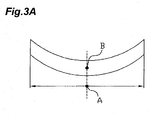
- the center in the vertical direction is defined as the mid-point B between the upper and lower edges of the reflecting surface on the vertical center line (the broken line in the drawing).
- the mid-point B is the "center" of the incidence-side element mirror.
- FIG. 3(B) depicts the reflecting surface of one of the emission-side element mirrors.
- the center C can easily be defined in an emission-side element mirror having, for example, a rectangular shape.
- EUV light reflected by the emission-side fly-eye mirror 14 can be made to converge appropriately on the surface of the mask M, whenever the mask is situated at an optimum position for such convergence.
- each of the lots of rays resulting from wavefront dividing and reflection of EUV light by the incidence-side fly-eye mirror 12 is incident on a respective element mirror of the emission-side fly-eye mirror 14.
- a secondary light source is formed, from the respective individual light-source images, at the reflective surface of the emission-side fly-eye mirror 14 or in the vicinity of that reflective surface.
- EUV light, from that secondary light source is reflected by the emission-side fly-eye mirror 14 and is led to the condensing optical system through an aperture stop (not shown) so as to be incident on the condenser mirror (a spherically convex mirror) 18 of the condensing optical system.
- the aperture stop determines the numerical aperture of the illumination light.
- the condenser mirror 18 comprises a substrate of glass, ceramic, metal, or the like, with a reflective surface coated with a multilayer film (e.g., alternating layers of Mo and Si).
- a multilayer film e.g., alternating layers of Mo and Si.
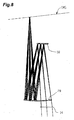
- optical eccentricity means that, as indicated in a diagram of the optical path of FIG. 4, the center of curvature C18 of the condenser mirror 18 is not on the normal N to the surface of the mask M, even if there is no deflection by the plane mirror 22 (FIG. 1); i.e., even when the beam of light reflected by the plane mirror 22 is expanded, as indicated in FIG. 4.
- the condenser mirror 20 comprises a substrate of glass, ceramic, metal, or the like, with a reflective surface coated with a multilayer film formed of alternating layers of molybdenum (Mo) and silicon (Si) to improve its reflectivity to EUV light.
- Mo molybdenum
- Si silicon
- the center of curvature C20 of the condenser mirror (a spherical mirror) 20 is also optically eccentric with respect to the normal N to the mask M surface (IMG) at the center of the irradiated region, as shown in FIG. 4. Consequently, compared to a situation in which there is no optical eccentricity with respect to the normal N, the degrees of freedom with which the condenser mirror 20 can be positioned are increased.
- EUV light reflected by the condenser mirror 20 is reflected and deflected by the plane mirror 22. This reflected and deflected EUV light uniformly illuminates, with superposition, the reflective mask M on which is formed a prescribed circuit pattern.
- the EUV light reflected by the reflection-type mask M forms a secondary light-source image at the pupil of the reflection-type projection-optical system PL.
- the projection-optical system PL projects the image of pattern formed on the mask M, onto the wafer W for exposure.
- the wafer W is coated with a resist, thereby forming a photosensitive substrate.
- the perpendicular line at the center of the effective aperture-stop plane at the emission-side fly-eye mirror 14 can be defined as a virtual optical axis A. It is useful to regard this virtual optical axis A as a reference.
- the center of curvature C18 of the convex mirror 18 and the center of curvature C20 of the concave mirror 20 are both at eccentric positions relative to the virtual optical axis A.
- the optical axis Ac of the condensing optical system is effectively defined by the straight line connecting the two centers of curvature C18 and C20.
- This eccentric configuration can be characterized in that the optical axis Ac of the condensing optical system is not parallel to the normal N to the mask M surface (IMG) at the center of the irradiated region of the mask. Also, this eccentric configuration can be characterized in that the optical axis Ac of the condensing optical system is also not parallel to the virtual optical axis A which is the perpendicular line at the center of the effective aperture-stop plane at the emission-side fly-eye mirror 14.
- the condensing optical system is configured with the optical axis Ac defined in this way, then there is no need for both the centers of curvature C18 and C20 of the convex mirror 18 and the concave mirror 20, respectively, to be eccentric with respect to the normal N or the virtual optical axis A, and a configuration is possible in which only one of the two centers of curvature C18 and C20 is eccentric.
- the condensing optical system in this embodiment comprises two reflecting mirrors, which are, in the order in which light arrives, the convex mirror 18 and the concave mirror 20.
- FIG. 4 shows the optical path of the condensing optical system of an exposure apparatus according to this embodiment
- FIG. 5 shows the optical path of a conventional condensing optical system having one concave mirror, such as the system included in the conventional exposure apparatus shown in FIG. 9.
- FIGS. 4 and 5 are drawn to the same scale.
- each of the reflecting mirrors is provided with appropriate power. Consequently, the mirrors are placed so as to form an extremely compact optical system compared to the conventional condensing optical system shown in FIG. 5.
- the focal length of a single convex lens is f
- the interval (distance) between the object-side focal point and the image-side focal point is 2f. If a positive lens, a negative lens, and a positive lens are combined in a three-lens optical system, the distance between the object-side focal point and the image-side focal point can be reduced to f or less.
- a condensing optical system as discussed above, that is telecentric at the mask has an object-side focal point located at the emission plane of the fly-eye optical system and an image-side focal point located at the mask (or at a plane conjugate to the mask), so that the distance between the object-side focal point and the image-side focal point is the entire length of the condensing optical system.
- a condensing optical system having a positive-negative-positive power arrangement can be realized that has a long focal length relative to its overall length.
- each of the element mirrors of the emission-side fly-eye mirror is tilted slightly relative to the others so that, overall, the emission-side fly-eye mirror exhibits the power of a positive lens. If the two mirrors were replaced with a lens system, the resulting optical system (both fly-eye mirrors and the condensing optical system) would have the power arrangement of a combination of a positive lens, a negative lens, and a positive lens. Consequently, the condensing optical system of this embodiment is extremely compact.
- the condensing optical system of this embodiment despite having a long focal length, can be situated at an optimum position. Also, the distance between the incidence-side fly-eye mirror and emission-side fly-eye mirror can be substantially longer than in a conventional system, allowing the respective angles of incidence of EUV light on the incidence-side fly-eye mirror and emission-side fly-eye mirror to be decreased. This, in turn, allows the reflectivity to EUV light of the incidence-side fly-eye mirror and emission-side fly-eye mirror to be increased relative to conventional systems, with consequent reduced loss of amount of EUV light.
- the respective inclinations of the multiple element mirrors of the emission-side fly-eye mirror are set such that the respective rays from the element mirrors converge, via the condensing optical system, at a point on the mask surface. That is, each of the reflection-type partial optical systems of the emission-side fly-eye optical system is provided with an inclination (tilt) such that light is reflected toward the axis of that fly-eye optical system. These individual inclinations are greater toward the periphery of the fly-eye optical system. Thus, the entire emission-side fly-eye optical system has a convergent effect like that of a concave mirror.
- the mask surface to be illuminated optimally with EUV light (illumination light) in a manner that prevents decreases in resolution, contrast, and the like on the wafer surface. Also, the wafer can be exposed at higher throughput with the fine pattern formed on the mask.
- EUV light illumination light
- the condensing optical system comprises two spherical mirrors that, in order from the incident-light side, are convex and concave.
- both mirrors may be aspherical.
- one of the mirrors can be spherical and the other can be aspherical.
- EUV light is used as the exposure light.
- laser light produced by, e.g., a KrF excimer laser, an ArF excimer laser, or an F 2 laser may be used as the exposure light.
- a reticle is illuminated by the illumination apparatus, and a projection-optical system is used for exposing a photosensitive substrate (wafer) with the pattern for transferring, defined on the mask.
- This general lithographic method can be used in the manufacture of microdevices (e.g., semiconductor devices, image-capture devices, liquid-crystal-display devices, thin-film magnetic heads, and the like).
- FIG. 6 depicts a flowchart of an exemplary method for manufacturing semiconductor devices (as exemplary microdevices). The method includes forming a prescribed circuit pattern on a wafer or similar as a photosensitive substrate using an exposure apparatus such as the embodiment described above.
- step S 301 of FIG. 6 a metal film is deposited onto each wafer in one lot.
- step S 302 a photoresist is applied onto the metal film on each wafer in the one lot.
- step S 303 an exposure apparatus such as the embodiment described above is used to perform lithographic exposures, by which images of the pattern defined on the mask are formed successively in each shot area of wafers in the one lot, using the projection-optical system.
- step S 304 After developing the photoresist on each wafer in the one lot in step S 304, each wafer in the one lots is etched (step S 305 ), using the photoresist pattern as a mask, so that a circuit pattern corresponding to the mask pattern is formed in each shot area on each wafer.
- steps S 301 -S 305 metal is deposited onto the wafer, photoresist is applied onto the metal film, and exposure, development, and etching steps are performed. Prior to these steps a silicon oxide film may be formed, if desired, on the wafer, after which the photoresist is deposited on the silicon oxide film, followed by exposure, development, etching, and other steps.
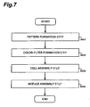
- a prescribed pattern (circuit pattern, electrode pattern, or the like) can be formed on a plate (e.g., glass substrate) so as to imprint a layer of a liquid-crystal-display device (a type of microdevice).
- a so-called photolithography step is performed in the pattern-formation step S 401 , in which the pattern of a mask is transferred onto a photosensitive substrate (glass substrate or the like onto which a photoresist has been deposited) to effect exposure using the exposure apparatus of the above embodiment.
- a prescribed pattern containing numerous electrodes or the like is formed on the photosensitive substrate.
- the exposed substrate is subjected to a development step, an etching step, a resist-removing step, and optionally other steps to form the prescribed pattern on the substrate. These steps can be followed by a color-filter-formation step S 402 .
- the color-filter-formation step S 402 multiple groups of three dots corresponding to R (red), G (green), and B (blue) are arranged in a matrix. Alternatively, multiple groups of three R, G, B stripes are arranged in a horizontal scan-line direction, to form a color filter.
- a cell-assembly step S 403 is executed, in which a substrate having the prescribed pattern formed in step S 401 , a color filter formed in step S 402 , and optionally other structures, are assembled into a liquid-crystal panel (liquid-crystal cells).
- liquid-crystal material is injected into gaps between the substrate (having a prescribed pattern formed in the pattern-formation step S 401 ) and the color filter formed in the color-filter-formation step S 402 , to fabricate a liquid-crystal panel (liquid-crystal cells).
- step S 404 electronic circuits required for operating display-action of the cells of the liquid-crystal panel (liquid-crystal cells), a backlight, and other components are installed, to complete fabrication of the liquid-crystal-display device.
- FIG. 8 shows the schematic configuration of an exemplary emission-side fly-eye mirror and condensing optical system of an illumination apparatus according to this example, as well as the position of the surface to be illuminated IMG.
- the configurations of the emission-side fly-eye mirror 14 and of the condensing optical system of this example are as described for the emission-side fly-eye mirror 14 and condenser mirrors 18, 20 of the embodiment shown in FIG. 1. Consequently, the reference symbols used in the following description are as used above in the description of the embodiment.
- Data for the emission-side fly-eye mirror 14 and condenser mirrors 18, 20 of the illumination apparatus of this embodiment are provided according to the format used in CODE V (Optical Research Associates), a type of optical-design software.
- CODE V design protocol the virtual optical axis A (FIG. 4) is regarded as the optical axis in the design process, and the optical data provided below are based on this approach.
- EPD is the diameter of the beam caused to be incident on the illumination apparatus
- DIM is the unit of length used
- WL indicates the wavelength of light rays used.
- the direction of the beam caused to be incident on the illumination apparatus also is indicated.
- XAN is the X-direction component of the angle made by the optical axis of the optical system
- YAN is the Y-direction component of the angle made by the optical axis of the optical system.
- 15 rays, each at a different angle with respect to the optical axis of this illumination apparatus, are incident on the optical system.
- the specifications are, in order from the left: surface number, surface radius of curvature (mm), distance to the next surface (mm), and material of the optical member.
- OBJ denotes the object plane
- STO is the aperture-stop plane
- INFINITY is infinity (e.g., when the radius of curvature is INFINITY, the surface is a plane)
- IMG is the image plane (surface to be illuminated).
- SPS XYP is a free-form surface represented by a power series in XY (i.e., a SPS XYP-XY polynomial aspherical surface).
- the SPS XYP surface includes 10th-order polynomial surfaces based on conics; the polynomial equation is expanded as x m y n (m+n ⁇ 10).
- Equation (1) is an equation for the SPS XYP surface (aspherical surface equation).
- the SCO coefficient C1 is the conic constant K
- C2 is the y coefficient Y
- C4 is the x 2 coefficient X2
- C6 is the y 2 coefficient Y2
- C8 is the x 2 y coefficient X2Y
- C10 is the y 3 coefficient Y3
- C11 is the x 4 coefficient X4
- C13 is the x 2 y 2 coefficient X2Y2
- C15 is the y 4 coefficient Y4
- C19 is the x 2 y 3 coefficient X2Y3
- C21 is the y 5 coefficient Y5.
- XDE, YDE, ZDE, ADE, BDE, CDE denote surface eccentricities, wherein “XDE” is the X-direction shift (mm), “YDE” is the Y-direction shift (mm), “ZDE” is the Z-direction shift (mm), “ADE” is the rotation (degrees) about the X-axis, “BDE” is the rotation (degrees) about the Y-axis, and “CDE” is the rotation (degrees) about the Z-axis.
- eccentricity occurs in a certain surface, from the next surface eccentricity and the like are represented according to new coordinates after the eccentricity is included. But, for surfaces denoted by “DAR,” eccentricity is represented independently, regardless of the eccentricity and the like of the surface preceding the surface denoted by DAR. Also, whenever a surface is denoted by “REFL,” the surface is a reflecting surface. Exemplary data are provided in Table 2, below.
- the free-form surface of the emission-side fly-eye mirror 14 is represented by virtually providing a virtual free-form surface lens ("kasou”), formed from glass having an extremely high refractive index.
- the refractive index of the virtual free-form surface lens (“kasou”) is 10,000.
- the respective centers of curvature of the convex mirror 18 and concave mirror 20 of the condensing optical system are optically eccentric with respect to the normal at the center of the illuminated region, as shown in FIG. 4.
- the degrees of freedom in the design and in the positioning of the condenser mirrors 18, 20 can be increased.
- the inclinations of the multiple element mirrors of the emission-side fly-eye mirror 14 are set such that, for each of the multiple element mirrors of the fly-eye mirror 14, individual rays converge on one point on the image plane IMG via the condenser mirrors 18, 20.
- the emission-side fly-eye mirror 14 can be configured so as to have a positive-power profile that is equivalent to a free-form curve.
- the beam reflected by the condenser mirrors 18, 20 can be made to converge appropriately on the surface to be illuminated (image plane IMG), positioned at an optimal position.
- Illumination apparatuses, exposure apparatuses, and microdevice-manufacturing methods according to the present invention are appropriate for use in the manufacture of high-performance semiconductor devices, liquid-crystal-display devices, thin-film magnetic heads, and other microdevices.
Landscapes
- Physics & Mathematics (AREA)
- General Physics & Mathematics (AREA)
- Optics & Photonics (AREA)
- Exposure And Positioning Against Photoresist Photosensitive Materials (AREA)
- Exposure Of Semiconductors, Excluding Electron Or Ion Beam Exposure (AREA)
- Microscoopes, Condenser (AREA)
- Lenses (AREA)
Abstract
Description
- This invention pertains to illumination apparatuses for manufacturing microdevices such as semiconductor devices, liquid-crystal-display devices, thin-film magnetic heads and the like in lithographic processes, exposure apparatus comprising the illumination apparatuses.
- In recent years, there has been progress in the commercialization of exposure apparatus that perform exposure by projection, onto a photosensitive substrate, of a mask pattern using extreme ultraviolet (EUV) light in the wavelength range of 5-40 nm as exposure light. In an EUVL (extreme ultraviolet lithography) exposure apparatus, optical materials are limited to materials that exhibit high transmittance at short wavelengths. Consequently, reflection-type optical systems are used (see, for example,
U.S. Pat. No. 6,452,661 andJapan Laid-open (Kokai) Patent Document No. Hei 11-312638 U.S. Pat. No. 6,452,661 , incorporated herein by reference). - An exposure apparatus as noted above is exemplified by the prior-art system shown in FIG. 9. A target material, supplied by a
nozzle 203, is irradiated at apoint 204 with laser light emitted from a non-EUV laser-light source 201 and condensed by a condensingelement 202. Thus, the target material receives an intensely concentrated dose of energy that converts the target material into a plasma that generates EUV light. The generated EUV light is condensed by acondensing mirror 205 and reflected by aconcave mirror 206. The EUV light then is incident on an incidence-side fly-eye mirror 207, in which numerous concave mirror segments are arranged in rows. The beam reflected by the incidence-side fly-eye mirror 207 passes through adiaphragm aperture 208 and is reflected by an emission-side fly-eye mirror 209, in which numerous concave mirror segments are arranged in rows. The beam again passes through thediaphragm aperture 208 and is incident on anoptical assembly 210. The beam reflected by theoptical assembly 210 is condensed by a condensingoptical assembly 211 for irradiation of amask 212. The beam carries an image of the pattern defined on theirradiated mask 212 as the beam passes through a projection-optical system 213, which projects the image onto a wafer (photosensitive substrate) 214. - In an illumination apparatus of a conventional exposure apparatus as summarized above, the incidence-side fly-
eye mirror 207 and the emission-side fly-eye mirror 208 are separated from each other by a short distance. Consequently, the incidence angle of the beam on the incidence-side fly-eye mirror 207 is large. However, in an EUVL exposure apparatus, in order to increase the reflectance of EUV light on a reflective layer, it is required that the EUV light be incident to the multilayer film at a small angle of incidence, i.e., nearly perpendicular to the film. To reduce the angle of incidence of EUV light on the incidence-side fly-eye mirror 207, the distance between the incidence-side fly-eye mirror 207 and the emission-side fly-eye mirror 209 must be increased. To accommodate this greater distance, the focal length of the condensingoptical assembly 211 would have to be increased. - When the focal length of the condensing
optical assembly 211 is increased, the condensingoptical assembly 211 is situated below the level of thewafer 214 rather than within the projection-optical system 213 as shown in FIG. 9. Because thewafer 214 moves in a scanning direction during exposure, placing the condensingoptical assembly 211 below the level of thewafer 214 would cause thewafer 214 to interfere physically with the condensingoptical assembly 211. Thus, in a conventional exposure apparatus as shown, it is difficult to satisfy both requirements of the condensingoptical assembly 211 being provided with a long focal length, and the distance between the incidence-side fly-eye mirror 207 and the emission-side fly-eye mirror 209 being increased so that EUV light is incident at an angle close to perpendicular on the reflecting surfaces of the incidence-side fly-eye mirror 207, to improve the reflectivity of the fly-eye mirrors. - In view of the above, the object of this invention is to provide an illumination apparatus that includes a condensing optical system or the like especially suitable for use in extreme ultraviolet lithography (EUVL), an exposure apparatus including such illumination apparatus, and microdevice-manufacturing methods performed using such exposure apparatus.
- The illumination apparatus of the present invention is used for illuminating a surface to be illuminated with illumination light emitted from a light source, the illumination apparatus comprising: an incidence-side reflection-type fly-eye optical system comprising multiple reflection-type partial optical systems arranged in rows; an emission-side reflection-type fly-eye optical system comprising multiple reflection-type partial optical systems arranged in rows such that the multiple reflection-type partial optical systems in the emission-side reflection-type fly-eye optical system respectively correspond to the multiple reflection-type partial optical systems in the incidence-side reflection-type fly-eye optical system; and a condensing optical system comprising two reflecting mirrors that guide the illumination light, reflected by the emission-side reflection-type fly-eye optical system, to the surface to be illuminated, wherein at least one of the two reflecting mirrors has a center of curvature that is optically eccentric with respect to a normal to the surface to be illuminated at the center of the illuminated region.
- In the illumination apparatus of the present invention, the two reflecting mirrors are spherical mirrors. In the illumination apparatus of the present invention, the two reflecting mirrors are aspherical mirrors. In the illumination apparatus of the present invention, the two reflecting mirrors are a spherical mirror and an aspherical mirror.
- According to the present invention, because the center of curvature of at least one of the two reflecting mirrors of the condensing optical system is optically eccentric with respect to the normal to the irradiated region of the surface to be illuminated at the center of the irradiated region, the degrees of freedom of configuration and location of the condensing optical system are increased relative to conventional illumination apparatuses that lack such optical eccentricity. Thus, the condensing optical system can be situated at an optimum position while allowing a substantial increase in the focal length of the condensing optical system and a substantial increase in the interval (distance) between the incidence-side fly-eye optical system and the emission-side fly-eye optical system. Thus, the angles of incidence of illumination light on the incidence-side fly-eye optical system and on the emission-side fly-eye optical system can be made small to improve the reflectivity of the incidence-side fly-eye optical system and the emission-side fly-eye optical system with respect to the illumination light and thus prevent loss of amount of illumination light. Whenever such an illumination apparatus is employed in an exposure apparatus, the mask surface (and hence the surface of the photosensitive substrate) can be optimally illuminated with exposure light. This restrains deteriorations of the resolution, contrast, and the like of the image formed on the photosensitive substrate, and allows the photosensitive substrate to be exposed with high throughput to the fine pattern defined on the mask.
- In the illumination apparatus of the present invention, inclinations of the multiple reflection-type partial optical systems in the incidence-side reflection-type fly-eye optical system are set such that individual rays from each of the multiple reflection-type partial optical systems reaching at respective centers of respective effective reflecting surfaces of the multiple reflection-type partial optical systems in the incidence-side reflection-type fly-eye optical system and reaching at respective centers of respective effective reflecting surfaces of multiple reflection-type partial optical systems in the emission-side reflection-type fly-eye optical system are converged by the condensing optical system at a point on the surface to be illuminated.
- According to the illumination apparatus of the present invention, the respective inclinations of the reflection-type partial optical systems of the emission-side fly-eye optical system are set such that individual rays from each of the multiple reflection-type partial optical systems converge via the condensing optical system at one point on the surface to be illuminated. Ie., each of the reflection-type partial optical systems of the emission-side fly-eye optical system is inclined (tilted) so as to reflect light toward the center of the reflection-type fly-eye optical system. The closer to the periphery, the greater the inclination from individual reflection-type partial optical systems. Thus, the fly-eye optical system exhibits a convergent action as if it were acting as a single concave mirror. Thus, the entire emission-side fly-eye optical system has positive power, which serves to converge illumination light reflected by the condensing optical system appropriately on the surface to be illuminated, which is positioned appropriately for such irradiation. Here, the effective concave-mirror action of the emission-side reflection-type fly-eye optical system is not limited to action that would be exhibited by a spherical concave mirror; the effective concave-mirror action alternatively can be similar to that of an aspherical surface (whether an aspherical surface having rotational symmetry or a so-called free-form curved surface having no symmetry axis).
- The exposure apparatus of the present invention is provided for transferring a pattern of a mask onto a photosensitive substrate, the exposure apparatus comprising an illumination apparatus of the present invention situated and configured to illuminate the mask.
- The exposure apparatus of the present invention comprises the illumination apparatus including a condensing optical system that is appropriate for use in EUVL. Thus, loss of amount of illumination light is prevented, which prevents declines in resolution, contrast, and the like of the image as formed on the photosensitive substrate. These benefits allow the photosensitive substrate to be exposed with high throughput to the detailed pattern defined on the mask.
- The microdevice-manufacturing method of the present invention comprises an exposure step of exposing a photosensitive substrate to a pattern on a reflective reticle, using an exposure apparatus of the present invention; and a development step of developing the photosensitive substrate exposed in the exposure step.
- In the microdevice-manufacturing method of the present invention, exposures are performed using an exposure apparatus including an optimal condensing optical system for use in EUVL illumination apparatus. Therefore, the microdevice-manufacturing method facilitates the production of microdevices having extremely detailed circuit patterns.
The exposure apparatus of the present invention comprises an incidence-side reflection-type fly-eye optical system comprising multiple reflection-type partial optical systems arranged in rows; an emission-side reflection-type fly-eye optical system comprising multiple reflection-type partial optical systems arranged in rows such that the multiple reflection-type partial optical systems in the emission-side reflection-type fly-eye optical system respectively correspond to the multiple reflection-type partial optical systems in the incidence-side reflection-type fly-eye optical system; and a condensing optical system comprising two reflecting mirrors that guide the illumination light, reflected by the emission-side reflection-type fly-eye optical system, to the surface to be illuminated, wherein the condensing optical system has an optical axis that passes through centers of curvature of the two reflecting mirrors but is not parallel to a normal to the surface to be illuminated at the center of the illuminated region.
The exposure apparatus of the present invention comprises an incidence-side reflection-type fly-eye optical system comprising multiple reflection-type partial optical systems arranged in rows; an emission-side reflection-type fly-eye optical system comprising multiple reflection-type partial optical systems arranged in rows such that the multiple reflection-type partial optical systems in the emission-side reflection-type fly-eye optical system respectively correspond to the multiple reflection-type partial optical systems in the incidence-side reflection-type fly-eye optical system; and a condensing optical system comprising two reflecting mirrors that guide the illumination light, reflected by the emission-side reflection-type fly-eye optical system, to the surface to be illuminated, wherein the condensing optical system has an optical axis that passes through centers of curvature of the two reflecting mirrors of the condensing optical system but is not parallel to a virtual optical axis defined as a perpendicular line passing through a center of an aperture plane of the emission-side reflection-type fly-eye optical system. The resulting eccentric configuration of the condensing optical system in the above described invention provides excellent illumination.
The exposure apparatus of the present invention comprises an incidence-side reflection-type fly-eye optical system comprising multiple reflection-type partial optical systems arranged in rows; an emission-side reflection-type fly-eye optical system comprising multiple reflection-type partial optical systems arranged in rows such that the multiple reflection-type partial optical systems in the emission-side reflection-type fly-eye optical system respectively correspond to the multiple reflection-type partial optical systems in the incidence-side reflection-type fly-eye optical system; and a condensing optical system comprising two reflecting mirrors that guide the illumination light, reflected by the emission-side reflection-type fly-eye optical system, to the surface to be illuminated, wherein the condensing optical system comprising an incidence-side convex mirror and an emission-side concave mirror. This condensing optical system provides a compact illumination-optical system while maintaining a large distance (interval) between the two fly-eye optical systems.
With the exposure apparatus of the present invention, the partial optical systems in the emission-side reflection-type fly-eye optical system are tilted with respective inclination angles, where the closer to a periphery thereof, the greater the inclination angles so that the entire emission-side reflection-type fly-eye optical system has a convergent action.. By using a subsequent condensing optical system having a convex mirror and a concave mirror, illumination-optical systems are provided that converge, then diverge, and then converge light passing through them. Ie., the illumination-optical systems have positive, negative, and positive powers. This configuration yields a more compact illumination-optical system.
The eccentric configuration of the condensing optical system of the exposure apparatus of the present invention provides a high degree of freedom of design, and excellent illumination performance. - Also, with an illumination apparatus of the present invention, since at least one of the centers of curvature of the convex mirror and concave mirror in the condensing optical system is optically eccentric with respect to a normal to the surface to be illuminated at the center of the illuminated region, the degree of freedom of design and positioning of the condensing optical system can be increased relative to conventional illumination apparatuses that lack such optical eccentricity. Hence, the condensing optical system can be positioned in an optimal position while allowing the focal length of the condensing optical system to be lengthened. Also realized is a lengthening of the distance (interval) between the incidence-side fly-eye optical system and the emission-side fly-eye optical system. Ie., the angles of incidence of illumination light incident on the incidence-side fly-eye optical system and the emission-side fly-eye optical system can be made small, which improves the respective reflectivities of the incidence-side fly-eye optical system and of the emission-side fly-eye optical system to the illumination light. The improved reflectivities prevent loss of amount of the illumination light. If such an illumination apparatus is employed in an exposure apparatus, the mask surface (and therefore the surface of the photosensitive substrate) can be illuminated in a more optimal manner. Thus, degradations in resolution, contrast, and the like of the image formed on the photosensitive substrate are prevented. Also achieved are high-throughput exposures of the photosensitive substrate with the detailed pattern formed on the mask.
- Also provided are microdevice-manufacturing methods of the present invention, in which exposure is performed using an exposure apparatus of the present invention. Therefore, illumination is performed by an illumination apparatus including an optimal condensing optical system for use in EUVL illumination apparatuses and thus, loss of amount of illumination light is prevented, which prevents deterioration of resolution, contrast, and the like, and facilitates manufacture of microdevices having extremely detailed circuit patterns.
-
- FIG. 1 is a view showing a schematic structure of an exposure apparatus in accordance with an embodiment.
- FIG. 2(A) is a plan view showing a configuration of an incidence-side fly-eye optical system.
- FIG. 2(B) is a plan view showing a configuration of an emission-side fly-eye optical system.
- FIG. 3(A) is a plan view of the reflecting surface of an element mirror of the incidence-side fly-eye optical system.
- FIG. 3(B) is a plan view of the reflecting surface of an element mirror of the emission-side fly-eye optical system.
- FIG. 4 is a diagram of the optical path associated with an embodiment of a condensing optical system.
- FIG. 5 is a diagram of the optical path associated with a conventional condensing optical system that utilizes a single mirror.
- FIG. 6 is a flowchart of an embodiment of a method for manufacturing semiconductor devices, as exemplary microdevices.
- FIG. 7 is a flowchart of an embodiment of a method for manufacturing liquid-crystal-display devices, as exemplary microdevices.
- FIG. 8 shows a schematic structure of an embodiment of a condensing optical system.
- FIG. 9 is a view showing a schematic structure of an exposure apparatus in accordance with a conventional exposure apparatus.
- Embodiments of exposure apparatus according to the present invention are described below with reference to the drawings. FIG. 1 shows a schematic structure of an exposure apparatus in accordance with this embodiment.
- The exposure apparatus uses EUV (extreme ultra violet) light having a wavelength in the range of approximately 5-40 nm. The apparatus performs exposures in a step-and-scan manner by which an image of a pattern, defined on a mask M, is transferred to a wafer W (photosensitive substrate) while moving the mask M and wafer W relative to the projection-optical system PL. The wafer W is "photosensitive" because it has a surficial layer of a photosensitive material (photoresist) applied to it. An illumination apparatus comprises a high-intensity laser-light source 2, a
condenser lens 4, a plasma light source 5 , a nozzle 6, a condenser mirror 8, acollector mirror 10, an incidence-side fly-eye mirror 12, an emission-side fly-eye mirror 14, condenser mirrors 18, 20, and the like. The illumination apparatus produces a beam of EUV light (illumination light) as exposure light. - In this exposure apparatus, because the transmissivity of air with respect to EUV light as exposure light is low, the optical path through which the EUV light propagates is enclosed in a vacuum chamber (not shown). Laser light emitted by the high-intensity laser-light source 2 (e.g., a YAG laser under semiconductor-laser excitation, an excimer laser, or other high-output laser) is condensed by the
condenser lens 4 to a point (condensed point) that serves as the plasma light source 5. Meanwhile, xenon (Xe) gas, krypton (Kr) gas, or other suitable target material for laser-plasma light source is ejected from the nozzle 6 at the condensed point. The extremely high intensity of laser light, emitted from the high-intensity laser-light source 2, impinging on the target material excites the target to a plasma condition. In the plasma, as the target material undergoes transitions to a low-potential state, they produce and emit EUV light, ultraviolet light of wavelength 100 nm and longer, visible light, and light of other wavelengths. - EUV light and the like emitted from the plasma light source 5 is incident on the condenser mirror 8. The condenser mirror 8 is positioned such that its first focal point, or vicinity thereof, is coincident with the condensed point serving as the plasma light source 5. The inner surface of the condenser mirror 8 is coated with a EUV reflecting film, for example a multilayer film consisting of alternating layers of molybdenum (Mo) and silicon (Si). As a result, only EUV light having a wavelength of approximately 13 nm from EUV light and the like incident on the condenser mirror 8 is reflected by the condenser mirror 8 and condensed to the second focal point of the condenser mirror 8. As another example, when EUV light having a wavelength of approximately 11 nm is used fro performing exposure, a multilayer film which reflects only EUV light having a wavelength of approximately 11 nm, for example a multilayer film of alternating layers of Mo and beryllium (Be) may be suitable.
- The reflected EUV light by the condenser mirror 8 is condensed at or near the second focal-point position of the condenser mirror 8 and is incident on the
collector mirror 10 as exposure light (illumination light). Thecollector mirror 10 includes a substrate of glass, ceramic, metal, or other material, on which is formed a multilayer film (e.g., alternating layers of Mo and Si) to achieve better reflection of incident EUV light. - EUV light reflected by the
collector mirror 10 is guided to a reflection-type fly-eye optical system that is used as an optical integrator. In the reflection-type fly-eye optical system, the EUV light is first incident on the incidence-side fly-eye mirror 12 (as an exemplary "incidence-side reflection-type fly-eye optical system"). The distance ("interval") between the incidence-side fly-eye mirror 12 and the emission-side fly-eye mirror 14 which is also included in the reflection-type fly-eye optical system in this embodiment is greater than in conventional illumination apparatuses. This allows EUV light to be incident, without being geometrically blocked, at a small angle from the perpendicular (ie., at a small angle of incidence) on the reflecting surface of the incidence-side fly-eye mirror 12. - Referring to FIG. 2(A), the incidence-side fly-
eye mirror 12 comprises multiple element mirrors (as exemplary "reflection-type partial optical systems"). The element mirrors are concave mirrors arranged densely in two dimensions (including rows). The incidence-side fly-eye mirror 12 is located so as to be optically conjugate (or nearly optically conjugate) to the surface of the mask M and the surface of the wafer W. The reflecting surface of each element mirror of the incidence-side fly-eye mirror 12 comprises a substrate of glass, ceramic, metal, or the like, and a surficial multilayer film (e.g., alternating layers of Mo and Si) to improve its reflectivity to EUV light. - The wavefront of EUV light incident to the incidence-side fly-
eye mirror 12 is divided . The EUV light whose wavefront was divided is reflected by the fly-eye mirror 12 and then passes through an aperture stop (not shown) to the emission-side fly-eye mirror (the emission-side reflection-type fly-eye optical system) 14 which is included in the reflection-type fly-eye optical system and on which the EUV light is incident also at an angle close to perpendicular (i.e., a small incidence angle). As shown in FIG. 2(B), the emission-side fly-eye mirror 14 comprises multiple element mirrors, which are concave mirrors ("reflection-type partial optical systems") that are arranged densely in two dimensions (including rows) and which respectively correspond to the multiple element mirrors of the incidence-side fly-eye mirror 12. The emission-side fly-eye mirror 14 is located so as to be optically conjugate (or nearly optically conjugate) to the pupil plane of the projection-optical system PL, described below. Each element mirror of the emission-side fly-eye mirror 14 comprises a substrate of glass, ceramic, metal, or the like, and a surficial multilayer film (e.g., alternating layers of Mo and Si) to improve its reflectivity to EUV light. Further details of the configurations of the incidence-side fly-eye mirror 12 and emission-side fly-eye mirror 14 are described inU.S. Pat. Nos. 6,452,661 and6,833,904 , incorporated herein by reference. - In the following discussion the multiple element mirrors of the emission-side fly-
eye mirror 14 are also called "emission-side element mirrors," and the multiple element mirrors of the incidence-side fly-eye mirror 12 are also called "incidence-side element mirrors." The respective inclinations of the emission-side element mirrors are set such that respective rays, that have reached the centers of the respective effective reflecting surfaces of the incidence-side element mirrors and that have reached the centers of respective effective reflecting surfaces of the emission-side element mirrors, do not converge on a single point or become collimated (made parallel) without passing through the condensing optical system described below. In other words, the reflecting surfaces of the emission-side element mirrors have respective prescribed inclinations such that respective rays reflected from the centers of the incidence-side element mirrors and reflected by the centers of the emission-side element mirrors (corresponding to the incidence-side element mirrors) are not collimated and do not converge on a single point on the surface of the mask M. Thus, the reflecting surfaces of the element mirrors of the emission-side fly-eye mirror 14 collectively have a convergent action equivalent to the action of an aspherical surface or of a free-form surface, as this fly-eye mirror exhibits an overall function of a concave mirror. - In FIG. 2(A) each of the incidence-side element mirrors has a same partial arc shape in the plan view. In FIG. 2(B) each of the emission-side element mirrors has a same rectangular shape in the plan view. Thus, respective rays that have passed through the same positions, e.g., respective rays that have passed through the centers of the element mirrors, converge at the same point on the mask M. FIG. 3(A) depicts the reflecting surface of one of the incidence-side element mirrors. As shown in FIG. 3(A), in an incidence-side element mirror having, for example, an arc shape as shown, the lateral-direction center A about which there is linear symmetry can easily be defined. The center in the vertical direction is defined as the mid-point B between the upper and lower edges of the reflecting surface on the vertical center line (the broken line in the drawing). The mid-point B is the "center" of the incidence-side element mirror. FIG. 3(B) depicts the reflecting surface of one of the emission-side element mirrors. In the FIG. 3(B), the center C can easily be defined in an emission-side element mirror having, for example, a rectangular shape.
- By making the entire reflective surface of the emission-side fly-
eye mirror 14 equivalent to a non-spherical or a free-form curved surface, in contrast to a spherical surface, EUV light reflected by the emission-side fly-eye mirror 14 can be made to converge appropriately on the surface of the mask M, whenever the mask is situated at an optimum position for such convergence. - As noted above, each of the lots of rays resulting from wavefront dividing and reflection of EUV light by the incidence-side fly-
eye mirror 12 is incident on a respective element mirror of the emission-side fly-eye mirror 14. Thus, a secondary light source is formed, from the respective individual light-source images, at the reflective surface of the emission-side fly-eye mirror 14 or in the vicinity of that reflective surface. EUV light, from that secondary light source, is reflected by the emission-side fly-eye mirror 14 and is led to the condensing optical system through an aperture stop (not shown) so as to be incident on the condenser mirror (a spherically convex mirror) 18 of the condensing optical system. The aperture stop determines the numerical aperture of the illumination light.
To improve its reflectivity to EUV light, thecondenser mirror 18 comprises a substrate of glass, ceramic, metal, or the like, with a reflective surface coated with a multilayer film (e.g., alternating layers of Mo and Si).
As indicated in FIG. 4, the center of curvature C18 of thecondenser mirror 18 which is a spherically convex mirror is optically eccentric with respect to the normal N to the irradiated region on the surface of the mask M (IMG) at the center of the illuminated region. Consequently, compared to a situation in which there is no optical eccentricity with respect to the normal N, the degrees of freedom with which thecondenser mirror 18 can be positioned are increased. Here, "optical eccentricity" means that, as indicated in a diagram of the optical path of FIG. 4, the center of curvature C18 of thecondenser mirror 18 is not on the normal N to the surface of the mask M, even if there is no deflection by the plane mirror 22 (FIG. 1); i.e., even when the beam of light reflected by the plane mirror 22 is expanded, as indicated in FIG. 4. - EUV light incident on the
condenser mirror 18 is reflected by thecondenser mirror 18 and is incident on the condenser mirror 20 (a spherically concave mirror) of the condensing optical system. Thecondenser mirror 20 comprises a substrate of glass, ceramic, metal, or the like, with a reflective surface coated with a multilayer film formed of alternating layers of molybdenum (Mo) and silicon (Si) to improve its reflectivity to EUV light. The center of curvature C20 of the condenser mirror (a spherical mirror) 20 is also optically eccentric with respect to the normal N to the mask M surface (IMG) at the center of the irradiated region, as shown in FIG. 4. Consequently, compared to a situation in which there is no optical eccentricity with respect to the normal N, the degrees of freedom with which thecondenser mirror 20 can be positioned are increased. - EUV light reflected by the
condenser mirror 20 is reflected and deflected by the plane mirror 22. This reflected and deflected EUV light uniformly illuminates, with superposition, the reflective mask M on which is formed a prescribed circuit pattern. The EUV light reflected by the reflection-type mask M forms a secondary light-source image at the pupil of the reflection-type projection-optical system PL. The projection-optical system PL projects the image of pattern formed on the mask M, onto the wafer W for exposure. The wafer W is coated with a resist, thereby forming a photosensitive substrate.
The eccentric configuration of theconvex mirror 18 andconcave mirror 20 of the condensing optical system, explained above with reference to FIG. 4, was described with the normal N to the mask M surface (IMG) at the center of the illuminated region being regarded as a reference. In optical design, the perpendicular line at the center of the effective aperture-stop plane at the emission-side fly-eye mirror 14 can be defined as a virtual optical axis A. It is useful to regard this virtual optical axis A as a reference. As indicated in FIG. 4, the center of curvature C18 of theconvex mirror 18 and the center of curvature C20 of theconcave mirror 20 are both at eccentric positions relative to the virtual optical axis A. The optical axis Ac of the condensing optical system is effectively defined by the straight line connecting the two centers of curvature C18 and C20. This eccentric configuration can be characterized in that the optical axis Ac of the condensing optical system is not parallel to the normal N to the mask M surface (IMG) at the center of the irradiated region of the mask. Also, this eccentric configuration can be characterized in that the optical axis Ac of the condensing optical system is also not parallel to the virtual optical axis A which is the perpendicular line at the center of the effective aperture-stop plane at the emission-side fly-eye mirror 14. If the condensing optical system is configured with the optical axis Ac defined in this way, then there is no need for both the centers of curvature C18 and C20 of theconvex mirror 18 and theconcave mirror 20, respectively, to be eccentric with respect to the normal N or the virtual optical axis A, and a configuration is possible in which only one of the two centers of curvature C18 and C20 is eccentric. - With an exposure apparatus according to this embodiment, because the optical axis of the condensing optical system comprising two
spherical mirrors convex mirror 18 and theconcave mirror 20. By appropriately tilting each of the element mirrors of the emission-side fly-eye mirror 14, an effective power (refractive power) results. This power is equivalent to a positive lens (equivalent to a concave mirror). - Whereas FIG. 4 shows the optical path of the condensing optical system of an exposure apparatus according to this embodiment, FIG. 5 shows the optical path of a conventional condensing optical system having one concave mirror, such as the system included in the conventional exposure apparatus shown in FIG. 9. FIGS. 4 and 5 are drawn to the same scale. In the condensing optical system of this embodiment each of the reflecting mirrors is provided with appropriate power. Consequently, the mirrors are placed so as to form an extremely compact optical system compared to the conventional condensing optical system shown in FIG. 5.
- Normally, if the focal length of a single convex lens (thin lens) is f, then the interval (distance) between the object-side focal point and the image-side focal point is 2f. If a positive lens, a negative lens, and a positive lens are combined in a three-lens optical system, the distance between the object-side focal point and the image-side focal point can be reduced to f or less. A condensing optical system, as discussed above, that is telecentric at the mask has an object-side focal point located at the emission plane of the fly-eye optical system and an image-side focal point located at the mask (or at a plane conjugate to the mask), so that the distance between the object-side focal point and the image-side focal point is the entire length of the condensing optical system. As a result, a condensing optical system having a positive-negative-positive power arrangement can be realized that has a long focal length relative to its overall length.
- In the optical-path configuration of the conventional condensing optical system with a single mirror shown in FIG. 5, only a single
concave mirror 211 is used. If the mirror were replaced with a lens system, the result would be equivalent to an optical system having a single positive lens. On the other hand, in the optical-path configuration of the condensing optical system according to this embodiment, a convex mirror and concave mirror are arranged, in that order from the fly-eye optical system side to the mask side. Also, the beam emitted from the emission-side fly-eye mirror is not a parallel beam, but rather a convergent beam. That is, each of the element mirrors of the emission-side fly-eye mirror is tilted slightly relative to the others so that, overall, the emission-side fly-eye mirror exhibits the power of a positive lens. If the two mirrors were replaced with a lens system, the resulting optical system (both fly-eye mirrors and the condensing optical system) would have the power arrangement of a combination of a positive lens, a negative lens, and a positive lens. Consequently, the condensing optical system of this embodiment is extremely compact. - The condensing optical system of this embodiment, despite having a long focal length, can be situated at an optimum position. Also, the distance between the incidence-side fly-eye mirror and emission-side fly-eye mirror can be substantially longer than in a conventional system, allowing the respective angles of incidence of EUV light on the incidence-side fly-eye mirror and emission-side fly-eye mirror to be decreased. This, in turn, allows the reflectivity to EUV light of the incidence-side fly-eye mirror and emission-side fly-eye mirror to be increased relative to conventional systems, with consequent reduced loss of amount of EUV light.
- The respective inclinations of the multiple element mirrors of the emission-side fly-eye mirror are set such that the respective rays from the element mirrors converge, via the condensing optical system, at a point on the mask surface. That is, each of the reflection-type partial optical systems of the emission-side fly-eye optical system is provided with an inclination (tilt) such that light is reflected toward the axis of that fly-eye optical system. These individual inclinations are greater toward the periphery of the fly-eye optical system. Thus, the entire emission-side fly-eye optical system has a convergent effect like that of a concave mirror. This allows the mask surface to be illuminated optimally with EUV light (illumination light) in a manner that prevents decreases in resolution, contrast, and the like on the wafer surface. Also, the wafer can be exposed at higher throughput with the fine pattern formed on the mask.
- In the exposure apparatus of this embodiment, the condensing optical system comprises two spherical mirrors that, in order from the incident-light side, are convex and concave. Alternatively, both mirrors may be aspherical. Further alternatively, one of the mirrors can be spherical and the other can be aspherical.
- In the exposure apparatus of this embodiment, EUV light is used as the exposure light. Alternatively, laser light produced by, e.g., a KrF excimer laser, an ArF excimer laser, or an F2 laser may be used as the exposure light.
- In the exposure apparatus of this embodiment, a reticle (mask) is illuminated by the illumination apparatus, and a projection-optical system is used for exposing a photosensitive substrate (wafer) with the pattern for transferring, defined on the mask. This general lithographic method can be used in the manufacture of microdevices (e.g., semiconductor devices, image-capture devices, liquid-crystal-display devices, thin-film magnetic heads, and the like). FIG. 6 depicts a flowchart of an exemplary method for manufacturing semiconductor devices (as exemplary microdevices). The method includes forming a prescribed circuit pattern on a wafer or similar as a photosensitive substrate using an exposure apparatus such as the embodiment described above.
- In step S301 of FIG. 6, a metal film is deposited onto each wafer in one lot. In step S 302 a photoresist is applied onto the metal film on each wafer in the one lot. In step S303 an exposure apparatus such as the embodiment described above is used to perform lithographic exposures, by which images of the pattern defined on the mask are formed successively in each shot area of wafers in the one lot, using the projection-optical system. After developing the photoresist on each wafer in the one lot in step S304, each wafer in the one lots is etched (step S305), using the photoresist pattern as a mask, so that a circuit pattern corresponding to the mask pattern is formed in each shot area on each wafer.
- By forming additional circuit patterns and the like on other layers, semiconductor devices or other devices are fabricated. In this microdevice-manufacturing method, because exposures are performed using the described embodiment of the exposure apparatus, reduced resolution, contrast, and the like in the images formed on the photosensitive substrate surface can be prevented. Consequently, microdevices having detailed circuit patterns can be produced at higher throughput. In steps S301-S305, metal is deposited onto the wafer, photoresist is applied onto the metal film, and exposure, development, and etching steps are performed. Prior to these steps a silicon oxide film may be formed, if desired, on the wafer, after which the photoresist is deposited on the silicon oxide film, followed by exposure, development, etching, and other steps.
- Using the embodiment of the exposure apparatus described above, a prescribed pattern (circuit pattern, electrode pattern, or the like) can be formed on a plate (e.g., glass substrate) so as to imprint a layer of a liquid-crystal-display device (a type of microdevice). An example of such a method is depicted in the flowchart of FIG. 7. In FIG. 7 a so-called photolithography step is performed in the pattern-formation step S401, in which the pattern of a mask is transferred onto a photosensitive substrate (glass substrate or the like onto which a photoresist has been deposited) to effect exposure using the exposure apparatus of the above embodiment. Thus, a prescribed pattern containing numerous electrodes or the like is formed on the photosensitive substrate. The exposed substrate is subjected to a development step, an etching step, a resist-removing step, and optionally other steps to form the prescribed pattern on the substrate. These steps can be followed by a color-filter-formation step S402.
- In the color-filter-formation step S402, multiple groups of three dots corresponding to R (red), G (green), and B (blue) are arranged in a matrix. Alternatively, multiple groups of three R, G, B stripes are arranged in a horizontal scan-line direction, to form a color filter. After the color-filter-formation step S402 a cell-assembly step S403 is executed, in which a substrate having the prescribed pattern formed in step S401, a color filter formed in
step S 402, and optionally other structures, are assembled into a liquid-crystal panel (liquid-crystal cells). In the cell-assembly step S403, for example, liquid-crystal material is injected into gaps between the substrate (having a prescribed pattern formed in the pattern-formation step S401) and the color filter formed in the color-filter-formation step S402, to fabricate a liquid-crystal panel (liquid-crystal cells). - In the module-assembly step S404 electronic circuits required for operating display-action of the cells of the liquid-crystal panel (liquid-crystal cells), a backlight, and other components are installed, to complete fabrication of the liquid-crystal-display device. By means of the above-described method of manufacture of a liquid-crystal-display device, because exposure is performed using the particular embodiment of exposure apparatus as described above, declines in resolution, contrast, and the like on the photosensitive substrate surface are avoided, and display devices having detailed circuit patterns are produced with high throughput.
- FIG. 8 shows the schematic configuration of an exemplary emission-side fly-eye mirror and condensing optical system of an illumination apparatus according to this example, as well as the position of the surface to be illuminated IMG. The configurations of the emission-side fly-
eye mirror 14 and of the condensing optical system of this example are as described for the emission-side fly-eye mirror 14 and condenser mirrors 18, 20 of the embodiment shown in FIG. 1. Consequently, the reference symbols used in the following description are as used above in the description of the embodiment. - Data for the emission-side fly-
eye mirror 14 and condenser mirrors 18, 20 of the illumination apparatus of this embodiment are provided according to the format used in CODE V (Optical Research Associates), a type of optical-design software. In the CODE V design protocol, the virtual optical axis A (FIG. 4) is regarded as the optical axis in the design process, and the optical data provided below are based on this approach. First, conditions for rays caused to be incident on the optical systems of the illumination apparatus of this example are described. In the following data, "EPD" is the diameter of the beam caused to be incident on the illumination apparatus, "DIM" is the unit of length used, and "WL" indicates the wavelength of light rays used. The direction of the beam caused to be incident on the illumination apparatus also is indicated. When Cartesian coordinates are used (with the Z-axis being the optical axis of the optical system), "XAN" is the X-direction component of the angle made by the optical axis of the optical system, and "YAN" is the Y-direction component of the angle made by the optical axis of the optical system. In this example, 15 rays, each at a different angle with respect to the optical axis of this illumination apparatus, are incident on the optical system. - EPD 166. 40000
DIM MM
WL 13. 50(nm) -
TABLE 1 (Direction of beam incidence) XAN 0.00000 0.00000 0.00000 0. 46553 0.46559 0.46553 0.93110 0.93110 0.93110 1.39672 1.39672 1.39672 1.86244 1.86244 1.86244 YAN 4.73228 4.87602 5.01980 4.70990 4.85364 4.99806 4.64216 4.78588 4.93226 4.62707 4.67077 4.82061 4.36106 4.50473 4.65987 eye mirror 14 and condenser mirrors 18, 20 of this example as optical members are provided. The specifications are, in order from the left: surface number, surface radius of curvature (mm), distance to the next surface (mm), and material of the optical member. Also, "OBJ" denotes the object plane, "STO" is the aperture-stop plane, "INFINITY" is infinity (e.g., when the radius of curvature is INFINITY, the surface is a plane), and "IMG" is the image plane (surface to be illuminated). Further, "SPS XYP" is a free-form surface represented by a power series in XY (i.e., a SPS XYP-XY polynomial aspherical surface). The SPS XYP surface includes 10th-order polynomial surfaces based on conics; the polynomial equation is expanded as xmyn (m+n≦ 10). The following Equation (1) is an equation for the SPS XYP surface (aspherical surface equation). - [Equation (1)]

in which z is the distance (sag amount) along the optical axis (Z-axis) of the emission-side fly-eye mirror 14, c is the vertex radius of curvature, K is the conic constant, and Cj are the xm ny SCO coefficients. Further, j-{(m-n)2+m+3n}/2-1. - In the optical-member specifications, the SCO coefficient C1 is the conic constant K, C2 is the y coefficient Y, C4 is the x2 coefficient X2, C6 is the y2 coefficient Y2, C8 is the x2y coefficient X2Y, C10 is the y3 coefficient Y3, C11 is the x4 coefficient X4, C13 is the x2y2 coefficient X2Y2, C15 is the y4 coefficient Y4, C17 is the x4y coefficient X4Y, C19 is the x2y3 coefficient X2Y3, and C21 is the y5 coefficient Y5.
- Further, XDE, YDE, ZDE, ADE, BDE, CDE denote surface eccentricities, wherein "XDE" is the X-direction shift (mm), "YDE" is the Y-direction shift (mm), "ZDE" is the Z-direction shift (mm), "ADE" is the rotation (degrees) about the X-axis, "BDE" is the rotation (degrees) about the Y-axis, and "CDE" is the rotation (degrees) about the Z-axis.
- Whenever eccentricity occurs in a certain surface, from the next surface eccentricity and the like are represented according to new coordinates after the eccentricity is included. But, for surfaces denoted by "DAR," eccentricity is represented independently, regardless of the eccentricity and the like of the surface preceding the surface denoted by DAR. Also, whenever a surface is denoted by "REFL," the surface is a reflecting surface. Exemplary data are provided in Table 2, below.
-
TABLE 2 (Optical member specifications) OBJ: INFINITY INFINITY STO: INFINITY 0.000000 2: 23357253.023 0.000000 'kasou' SPS XYP SCO K:-1.2615E+08 Y:-2.8043E-06 X2:-1.8313E-08 Y2:-1.8560E-08 X2Y:1.6132E-12 Y3:1.6118E-12 X4:-4.2860E-16 X2Y2:-6.9295E-16 Y4:-3.6733E-16 X4Y:-2.8616E-19 X2Y3:-6.0085E-19 Y5:-2.3244E-19 3: -23357253.02 969.999967 4: 1281.70038 870.000000 REFL XDE:0.000000 YDE:80.427242 ZDE:0.000000 DAR ADE:0.000000 BDE:0.000000 CDE:0.000000 5: 1691.15218 1300.000000 REFL XDE:0.000000 YDE:134.242815 ZDE:0.000000 DAR ADE:0.000000 BDE:0.000000 CDE:0.000000 6: INFINITY 0.000000 XDE:0.000000 YDE:144.442224 ZDE:0.000000 ADE:7.313410 BDE:0.000000 CDE:0.000000 IMG: INFINITY 0.000000 eye mirror 14 having power equivalent to such a free-form curve, the free-form surface of the emission-side fly-eye mirror 14 is represented by virtually providing a virtual free-form surface lens ("kasou"), formed from glass having an extremely high refractive index. The refractive index of the virtual free-form surface lens ("kasou") is 10,000. - By means of an illumination apparatus of this example, the respective centers of curvature of the
convex mirror 18 andconcave mirror 20 of the condensing optical system are optically eccentric with respect to the normal at the center of the illuminated region, as shown in FIG. 4. Thus, the degrees of freedom in the design and in the positioning of the condenser mirrors 18, 20 can be increased. Also, the inclinations of the multiple element mirrors of the emission-side fly-eye mirror 14 are set such that, for each of the multiple element mirrors of the fly-eye mirror 14, individual rays converge on one point on the image plane IMG via the condenser mirrors 18, 20. In addition, the emission-side fly-eye mirror 14 can be configured so as to have a positive-power profile that is equivalent to a free-form curve. Hence the beam reflected by the condenser mirrors 18, 20 can be made to converge appropriately on the surface to be illuminated (image plane IMG), positioned at an optimal position. - Illumination apparatuses, exposure apparatuses, and microdevice-manufacturing methods according to the present invention are appropriate for use in the manufacture of high-performance semiconductor devices, liquid-crystal-display devices, thin-film magnetic heads, and other microdevices.
Claims (15)
- An illumination apparatus for illuminating a surface to be illuminated with illumination light emitted from a light source, the illumination apparatus comprising:an incidence-side reflection-type fly-eye optical system comprising multiple reflection-type partial optical systems arranged in rows;an emission-side reflection-type fly-eye optical system comprising multiple reflection-type partial optical systems arranged in rows such that the multiple reflection-type partial optical systems in the emission-side reflection-type fly-eye optical system respectively correspond to the multiple reflection-type partial optical systems in the incidence-side reflection-type fly-eye optical system; anda condensing optical system comprising two reflecting mirrors that guide the illumination light, reflected by the emission-side reflection-type fly-eye optical system, to the surface to be illuminated, wherein at least one of the two reflecting mirrors has a center of curvature that is optically eccentric with respect to a normal to the surface to be illuminated at the center of the illuminated region.
- The illumination apparatus according to claim 1, wherein the two reflecting mirrors are spherical mirrors.
- The illumination apparatus according to claim 1, wherein the two reflecting mirrors are aspherical mirrors.
- The illumination apparatus according to claim 1, wherein the two reflecting mirrors are a spherical mirror and an aspherical mirror, respectively.
- The illumination apparatus according to claims 1-4, wherein:inclinations of the multiple reflection-type partial optical systems in the incidence-side reflection-type fly-eye optical system are set such that rays reaching at respective centers of respective effective reflecting surfaces of the multiple reflection-type partial optical systems in the incidence-side reflection-type fly-eye optical system and reaching at respective centers of respective effective reflecting surfaces of multiple reflection-type partial optical systems in the emission-side reflection-type fly-eye optical system are converged by the condensing optical system at a point on the surface to be illuminated.
- An exposure apparatus for transferring a pattern of a mask onto a photosensitive substrate, the exposure apparatus comprising an illumination apparatus as defined in any one of claims 1-5 situated and configured to illuminate the mask.
- A method for manufacturing microdevices, comprising:an exposure step of exposing a photosensitive substrate to a pattern on a reflective reticle, using an exposure apparatus as defined in claim 6; anda development step of developing the photosensitive substrate exposed in the exposure step.
- An exposure apparatus comprising an illumination apparatus for illuminating a surface to be illuminated with illumination light emitted from a light source, further comprising:an incidence-side reflection-type fly-eye optical system comprising multiple reflection-type partial optical systems arranged in rows;an emission-side reflection-type fly-eye optical system comprising multiple reflection-type partial optical systems arranged in rows such that the multiple reflection-type partial optical systems in the emission-side reflection-type fly-eye optical system respectively correspond to the multiple reflection-type partial optical systems in the incidence-side reflection-type fly-eye optical system; anda condensing optical system comprising two reflecting mirrors that guide the illumination light, reflected by the emission-side reflection-type fly-eye optical system, to the surface to be illuminated,wherein the condensing optical system has an optical axis that passes through centers of curvature of the two reflecting mirrors but is not parallel to a normal to the surface to be illuminated at the center of the illuminated region.
- An exposure apparatus comprising an illumination apparatus for illuminating a surface to be illuminated with illumination light emitted from a light source, further comprising:an incidence-side reflection-type fly-eye optical system comprising multiple reflection-type partial optical systems arranged in rows;an emission-side reflection-type fly-eye optical system comprising multiple reflection-type partial optical systems arranged in rows such that the multiple reflection-type partial optical systems in the emission-side reflection-type fly-eye optical system respectively correspond to the multiple reflection-type partial optical systems in the incidence-side reflection-type fly-eye optical system; anda condensing optical system comprising two reflecting mirrors that guide the illumination light, reflected by the emission-side reflection-type fly-eye optical system, to the surface to be illuminated,wherein the condensing optical system has an optical axis that passes through centers of curvature of the two reflecting mirrors of the condensing optical system but is not parallel to a virtual optical axis defined as a perpendicular line passing through a center of an aperture plane of the emission-side reflection-type fly-eye optical system.
- An exposure apparatus comprising an illumination apparatus for illuminating a surface to be illuminated with illumination light emitted from a light source, further comprising:an incidence-side reflection-type fly-eye optical system comprising multiple reflection-type partial optical systems arranged in rows;an emission-side reflection-type fly-eye optical system comprising multiple reflection-type partial optical systems arranged in rows such that the multiple reflection-type partial optical systems in the emission-side reflection-type fly-eye optical system respectively correspond to the multiple reflection-type partial optical systems in the incidence-side reflection-type fly-eye optical system; anda condensing optical system comprising two reflecting mirrors that guide the illumination light, reflected by the emission-side reflection-type fly-eye optical system, to the surface to be illuminated, wherein the condensing optical system comprising an incidence-side convex mirror and an emission-side concave mirror.
- The exposure apparatus according to claim 10, wherein:the partial optical systems in the emission-side reflection-type fly-eye optical system are tilted with respective inclination angles, where the closer to a periphery thereof, the greater the inclination angles so that the entire emission-side reflection-type fly-eye optical system has a convergent action.
- The exposure apparatus according to claim 11 wherein:at least one of the centers of curvature of the convex mirror and concave mirror in the condensing optical system is optically eccentric with respect to a normal to the surface to be illuminated at the center of the illuminated region.
- The exposure apparatus according to claim 11, wherein:at least one of the centers of curvature of the convex mirror and concave mirror is eccentric with respect to a virtual optical axis defined as a perpendicular line passing through a center of an aperture plane of the emission-side reflection-type fly-eye optical system.
- The exposure apparatus according to claim 11, wherein:the condensing optical system has an optical axis that passes through the respective centers of curvature of the convex mirror and the concave mirror but is not parallel to a normal to the surface to be illuminated at the center of the illuminated region.
- The exposure apparatus according to claim 11, wherein:the condensing optical system has an optical axis that passes through respective centers of curvature of the convex mirror and the concave mirror but is not parallel to a virtual optical axis defined as a perpendicular line passing through a center of an aperture plane of the emission-side reflection-type fly-eye optical system.
Applications Claiming Priority (2)
| Application Number | Priority Date | Filing Date | Title |
|---|---|---|---|
| JP2004332769 | 2004-11-17 | ||
| PCT/JP2005/020928 WO2006054544A1 (en) | 2004-11-17 | 2005-11-15 | Lighting apparatus, exposure apparatus and micro device manufacturing method |
Publications (2)
| Publication Number | Publication Date |
|---|---|
| EP1814147A1 true EP1814147A1 (en) | 2007-08-01 |
| EP1814147A4 EP1814147A4 (en) | 2010-06-02 |
Family
ID=36407087
Family Applications (1)
| Application Number | Title | Priority Date | Filing Date |
|---|---|---|---|
| EP05807103A Withdrawn EP1814147A4 (en) | 2004-11-17 | 2005-11-15 | LIGHTING APPARATUS, EXPOSURE APPARATUS, AND METHOD FOR MANUFACTURING MICRO DEVICE |
Country Status (7)
| Country | Link |
|---|---|
| US (2) | US7446856B2 (en) |
| EP (1) | EP1814147A4 (en) |
| JP (1) | JP4844398B2 (en) |
| KR (1) | KR101119576B1 (en) |
| CN (1) | CN101006557A (en) |
| TW (1) | TWI486714B (en) |
| WO (1) | WO2006054544A1 (en) |
Cited By (1)
| Publication number | Priority date | Publication date | Assignee | Title |
|---|---|---|---|---|
| WO2015036225A1 (en) * | 2013-09-11 | 2015-03-19 | Carl Zeiss Smt Gmbh | Illumination optical unit for euv microlithography |
Families Citing this family (11)
| Publication number | Priority date | Publication date | Assignee | Title |
|---|---|---|---|---|
| DE19903807A1 (en) * | 1998-05-05 | 1999-11-11 | Zeiss Carl Fa | EUV illumination system especially for microlithography in the production of electronic components with sub-micron structure widths |
| JP4844398B2 (en) * | 2004-11-17 | 2011-12-28 | 株式会社ニコン | Illumination apparatus, exposure apparatus, and microdevice manufacturing method |
| DE102006020734A1 (en) * | 2006-05-04 | 2007-11-15 | Carl Zeiss Smt Ag | Illumination system for the EUV lithography and first and second optical element for use in such a lighting system |
| EP1950594A1 (en) * | 2007-01-17 | 2008-07-30 | Carl Zeiss SMT AG | Imaging optical system, projection illumination unit for microlithography with such an optical system, method for manufacturing a microstructured component with such a projection illumination unit, microstructured component produced by the manufacturing method and use of such an optical system |
| US20090040493A1 (en) * | 2007-08-09 | 2009-02-12 | Hideki Komatsuda | Illumination optical system, illumination optical apparatus, exposure apparatus, and device manufacturing method |
| US7719661B2 (en) * | 2007-11-27 | 2010-05-18 | Nikon Corporation | Illumination optical apparatus, exposure apparatus, and method for producing device |
| CN101946190B (en) * | 2008-02-15 | 2013-06-19 | 卡尔蔡司Smt有限责任公司 | Facet mirrors used in projection exposure equipment for microlithography |
| US8497977B2 (en) * | 2009-03-12 | 2013-07-30 | Nikon Corporation | Optical integrator, illumination optical system, exposure apparatus, and device manufacturing method |
| CN104460242B (en) * | 2014-12-11 | 2016-04-27 | 北京理工大学 | A kind of extreme ultraviolet photolithographic illuminator based on free form surface formula diaphragm compound eye |
| TWI706235B (en) * | 2016-06-20 | 2020-10-01 | 日商尼康股份有限公司 | Euv lithography system for dense line patterning |
| US11042097B1 (en) * | 2019-12-31 | 2021-06-22 | Soulnano Limited | Multi-mirror UV-LED optical lithography system |
Family Cites Families (13)
| Publication number | Priority date | Publication date | Assignee | Title |
|---|---|---|---|---|
| JP4238390B2 (en) | 1998-02-27 | 2009-03-18 | 株式会社ニコン | LIGHTING APPARATUS, EXPOSURE APPARATUS PROVIDED WITH THE ILLUMINATION APPARATUS, AND METHOD FOR MANUFACTURING SEMICONDUCTOR DEVICE USING THE EXPOSURE APPARATUS |
| US6833904B1 (en) | 1998-02-27 | 2004-12-21 | Nikon Corporation | Exposure apparatus and method of fabricating a micro-device using the exposure apparatus |
| US6858853B2 (en) * | 1998-05-05 | 2005-02-22 | Carl Zeiss Smt Ag | Illumination system particularly for microlithography |
| DE10138313A1 (en) * | 2001-01-23 | 2002-07-25 | Zeiss Carl | Collector for lighting systems with a wavelength <193 nm |
| US6947124B2 (en) * | 1998-05-05 | 2005-09-20 | Carl Zeiss Smt Ag | Illumination system particularly for microlithography |
| US6195201B1 (en) * | 1999-01-27 | 2001-02-27 | Svg Lithography Systems, Inc. | Reflective fly's eye condenser for EUV lithography |
| JP3605055B2 (en) * | 2001-07-31 | 2004-12-22 | キヤノン株式会社 | Illumination optical system, exposure apparatus and device manufacturing method |
| DE60217771T3 (en) * | 2001-07-27 | 2012-02-09 | Canon K.K. | Exposure system, projection exposure apparatus and method of making an article |
| JP3605053B2 (en) * | 2001-07-27 | 2004-12-22 | キヤノン株式会社 | Illumination optical system, exposure apparatus and device manufacturing method |
| DE60312871T2 (en) * | 2002-08-26 | 2007-12-20 | Carl Zeiss Smt Ag | GRID BASED SPECTRAL FILTER FOR SUPPRESSING RADIATION OUTSIDE THE UTILITY BAND IN AN EXTREMELY ULTRAVIOLET LITHOGRAPHY SYSTEM |
| US7417708B2 (en) | 2002-10-25 | 2008-08-26 | Nikon Corporation | Extreme ultraviolet exposure apparatus and vacuum chamber |
| AU2003277515A1 (en) | 2002-10-25 | 2004-05-13 | Nikon Corporation | Extreme ultraviolet light exposure system and vacuum chamber |
| JP4844398B2 (en) * | 2004-11-17 | 2011-12-28 | 株式会社ニコン | Illumination apparatus, exposure apparatus, and microdevice manufacturing method |
-
2005
- 2005-11-15 JP JP2006545056A patent/JP4844398B2/en not_active Expired - Fee Related
- 2005-11-15 EP EP05807103A patent/EP1814147A4/en not_active Withdrawn
- 2005-11-15 WO PCT/JP2005/020928 patent/WO2006054544A1/en not_active Ceased
- 2005-11-15 CN CNA2005800282350A patent/CN101006557A/en active Pending
- 2005-11-15 KR KR1020077005412A patent/KR101119576B1/en not_active Expired - Fee Related
- 2005-11-16 US US11/281,785 patent/US7446856B2/en active Active
- 2005-11-17 TW TW094140395A patent/TWI486714B/en not_active IP Right Cessation
-
2008
- 2008-09-29 US US12/240,804 patent/US20090033903A1/en not_active Abandoned
Cited By (2)
| Publication number | Priority date | Publication date | Assignee | Title |
|---|---|---|---|---|
| WO2015036225A1 (en) * | 2013-09-11 | 2015-03-19 | Carl Zeiss Smt Gmbh | Illumination optical unit for euv microlithography |
| US9841683B2 (en) | 2013-09-11 | 2017-12-12 | Carl Zeiss Smt Gmbh | Illumination optical unit for EUV projection lithography |
Also Published As
| Publication number | Publication date |
|---|---|
| KR20070085226A (en) | 2007-08-27 |
| US20060170894A1 (en) | 2006-08-03 |
| TW200622513A (en) | 2006-07-01 |
| US20090033903A1 (en) | 2009-02-05 |
| EP1814147A4 (en) | 2010-06-02 |
| CN101006557A (en) | 2007-07-25 |
| KR101119576B1 (en) | 2012-03-16 |
| WO2006054544A1 (en) | 2006-05-26 |
| TWI486714B (en) | 2015-06-01 |
| JPWO2006054544A1 (en) | 2008-05-29 |
| JP4844398B2 (en) | 2011-12-28 |
| US7446856B2 (en) | 2008-11-04 |
Similar Documents
| Publication | Publication Date | Title |
|---|---|---|
| US20090033903A1 (en) | Illumination systems, exposure apparatus, and microdevice-manufacturing methods using same | |
| JP2003114387A (en) | Catadioptric optical system and projection exposure apparatus having the optical system | |
| EP1450209A1 (en) | Catoptric projection optical system | |
| US7232233B2 (en) | Catoptric reduction projection optical system and exposure apparatus using the same | |
| JP2004333761A (en) | Catadioptric projection optical system, exposure apparatus, and exposure method | |
| US7486439B2 (en) | Projection optical system, exposure apparatus and device fabricating method | |
| EP1335228B1 (en) | Catoptric projection system, exposure apparatus and device fabrication method using the same | |
| JP2004029625A (en) | Projection optical system, exposure apparatus and exposure method | |
| US6860610B2 (en) | Reflection type projection optical system, exposure apparatus and device fabrication method using the same | |
| JP5077565B2 (en) | Illumination optical apparatus, exposure apparatus, and device manufacturing method | |
| US20040125353A1 (en) | Projection optical system and exposure apparatus equipped with the projection optical system | |
| US20100103394A1 (en) | Reflection projection optical system, exposure apparatus, and method of manufacturing device | |
| JP2004170869A (en) | Imaging optical system, exposure apparatus and exposure method | |
| EP1513019B1 (en) | Projection optical system, exposure apparatus and device fabricating method | |
| EP1471389B1 (en) | Projection optical system | |
| WO2002095811A1 (en) | Lighting optical device, exposure system, and production method of micro device | |
| JP2004023020A (en) | Projection optical system and reduction projection exposure apparatus | |
| HK1101727A (en) | Lighting apparatus, exposure apparatus and micro device manufacturing method | |
| JP2004080021A (en) | Method and apparatus for adjusting optical system, exposure apparatus | |
| JP2004093953A (en) | Projection optical system, exposure apparatus, and micro device manufacturing method | |
| JP2004258178A (en) | Projection optical system and exposure apparatus having the projection optical system | |
| JP2004022722A (en) | Projection optical system and exposure apparatus having the projection optical system | |
| JP2004029458A (en) | Projection optical system and reduction projection exposure apparatus | |
| JP2006019476A (en) | Exposure apparatus and microdevice manufacturing method | |
| JP2000098229A (en) | Reflection reduction projection optical system, projection exposure apparatus having the optical system, and exposure method using the apparatus |
Legal Events
| Date | Code | Title | Description |
|---|---|---|---|
| PUAI | Public reference made under article 153(3) epc to a published international application that has entered the european phase |
Free format text: ORIGINAL CODE: 0009012 |
|
| 17P | Request for examination filed |
Effective date: 20070420 |
|
| AK | Designated contracting states |
Kind code of ref document: A1 Designated state(s): AT BE BG CH CY CZ DE DK EE ES FI FR GB GR HU IE IS IT LI LT LU LV MC NL PL PT RO SE SI SK TR |
|
| REG | Reference to a national code |
Ref country code: HK Ref legal event code: DE Ref document number: 1101727 Country of ref document: HK |
|
| DAX | Request for extension of the european patent (deleted) | ||
| A4 | Supplementary search report drawn up and despatched |
Effective date: 20100503 |
|
| RAP1 | Party data changed (applicant data changed or rights of an application transferred) |
Owner name: NIKON CORPORATION |
|
| STAA | Information on the status of an ep patent application or granted ep patent |
Free format text: STATUS: THE APPLICATION IS DEEMED TO BE WITHDRAWN |
|
| 18D | Application deemed to be withdrawn |
Effective date: 20100721 |
|
| REG | Reference to a national code |
Ref country code: HK Ref legal event code: WD Ref document number: 1101727 Country of ref document: HK |