EP1813494A1 - Vehicle control apparatus having event management unit - Google Patents
Vehicle control apparatus having event management unit Download PDFInfo
- Publication number
- EP1813494A1 EP1813494A1 EP07000894A EP07000894A EP1813494A1 EP 1813494 A1 EP1813494 A1 EP 1813494A1 EP 07000894 A EP07000894 A EP 07000894A EP 07000894 A EP07000894 A EP 07000894A EP 1813494 A1 EP1813494 A1 EP 1813494A1
- Authority
- EP
- European Patent Office
- Prior art keywords
- unit
- input
- event
- output
- signal
- Prior art date
- Legal status (The legal status is an assumption and is not a legal conclusion. Google has not performed a legal analysis and makes no representation as to the accuracy of the status listed.)
- Granted
Links
- 238000012545 processing Methods 0.000 claims abstract description 31
- 238000004891 communication Methods 0.000 claims abstract description 30
- 238000012546 transfer Methods 0.000 claims description 52
- 238000010586 diagram Methods 0.000 description 22
- 238000000034 method Methods 0.000 description 19
- 230000008569 process Effects 0.000 description 16
- 230000005540 biological transmission Effects 0.000 description 14
- 238000005259 measurement Methods 0.000 description 7
- 239000000758 substrate Substances 0.000 description 4
- 230000002093 peripheral effect Effects 0.000 description 3
- 230000009467 reduction Effects 0.000 description 2
- 239000000446 fuel Substances 0.000 description 1
- 230000006872 improvement Effects 0.000 description 1
- 230000010354 integration Effects 0.000 description 1
- 238000012986 modification Methods 0.000 description 1
- 230000004048 modification Effects 0.000 description 1
- 238000000059 patterning Methods 0.000 description 1
- 230000001360 synchronised effect Effects 0.000 description 1
Images






Classifications
-
- B—PERFORMING OPERATIONS; TRANSPORTING
- B60—VEHICLES IN GENERAL
- B60W—CONJOINT CONTROL OF VEHICLE SUB-UNITS OF DIFFERENT TYPE OR DIFFERENT FUNCTION; CONTROL SYSTEMS SPECIALLY ADAPTED FOR HYBRID VEHICLES; ROAD VEHICLE DRIVE CONTROL SYSTEMS FOR PURPOSES NOT RELATED TO THE CONTROL OF A PARTICULAR SUB-UNIT
- B60W50/00—Details of control systems for road vehicle drive control not related to the control of a particular sub-unit, e.g. process diagnostic or vehicle driver interfaces
-
- B—PERFORMING OPERATIONS; TRANSPORTING
- B60—VEHICLES IN GENERAL
- B60G—VEHICLE SUSPENSION ARRANGEMENTS
- B60G2800/00—Indexing codes relating to the type of movement or to the condition of the vehicle and to the end result to be achieved by the control action
- B60G2800/85—System Prioritisation
-
- B—PERFORMING OPERATIONS; TRANSPORTING
- B60—VEHICLES IN GENERAL
- B60W—CONJOINT CONTROL OF VEHICLE SUB-UNITS OF DIFFERENT TYPE OR DIFFERENT FUNCTION; CONTROL SYSTEMS SPECIALLY ADAPTED FOR HYBRID VEHICLES; ROAD VEHICLE DRIVE CONTROL SYSTEMS FOR PURPOSES NOT RELATED TO THE CONTROL OF A PARTICULAR SUB-UNIT
- B60W10/00—Conjoint control of vehicle sub-units of different type or different function
- B60W10/04—Conjoint control of vehicle sub-units of different type or different function including control of propulsion units
-
- B—PERFORMING OPERATIONS; TRANSPORTING
- B60—VEHICLES IN GENERAL
- B60W—CONJOINT CONTROL OF VEHICLE SUB-UNITS OF DIFFERENT TYPE OR DIFFERENT FUNCTION; CONTROL SYSTEMS SPECIALLY ADAPTED FOR HYBRID VEHICLES; ROAD VEHICLE DRIVE CONTROL SYSTEMS FOR PURPOSES NOT RELATED TO THE CONTROL OF A PARTICULAR SUB-UNIT
- B60W10/00—Conjoint control of vehicle sub-units of different type or different function
- B60W10/10—Conjoint control of vehicle sub-units of different type or different function including control of change-speed gearings
-
- B—PERFORMING OPERATIONS; TRANSPORTING
- B60—VEHICLES IN GENERAL
- B60W—CONJOINT CONTROL OF VEHICLE SUB-UNITS OF DIFFERENT TYPE OR DIFFERENT FUNCTION; CONTROL SYSTEMS SPECIALLY ADAPTED FOR HYBRID VEHICLES; ROAD VEHICLE DRIVE CONTROL SYSTEMS FOR PURPOSES NOT RELATED TO THE CONTROL OF A PARTICULAR SUB-UNIT
- B60W10/00—Conjoint control of vehicle sub-units of different type or different function
- B60W10/18—Conjoint control of vehicle sub-units of different type or different function including control of braking systems
- B60W10/184—Conjoint control of vehicle sub-units of different type or different function including control of braking systems with wheel brakes
-
- B—PERFORMING OPERATIONS; TRANSPORTING
- B60—VEHICLES IN GENERAL
- B60W—CONJOINT CONTROL OF VEHICLE SUB-UNITS OF DIFFERENT TYPE OR DIFFERENT FUNCTION; CONTROL SYSTEMS SPECIALLY ADAPTED FOR HYBRID VEHICLES; ROAD VEHICLE DRIVE CONTROL SYSTEMS FOR PURPOSES NOT RELATED TO THE CONTROL OF A PARTICULAR SUB-UNIT
- B60W10/00—Conjoint control of vehicle sub-units of different type or different function
- B60W10/20—Conjoint control of vehicle sub-units of different type or different function including control of steering systems
-
- B—PERFORMING OPERATIONS; TRANSPORTING
- B60—VEHICLES IN GENERAL
- B60W—CONJOINT CONTROL OF VEHICLE SUB-UNITS OF DIFFERENT TYPE OR DIFFERENT FUNCTION; CONTROL SYSTEMS SPECIALLY ADAPTED FOR HYBRID VEHICLES; ROAD VEHICLE DRIVE CONTROL SYSTEMS FOR PURPOSES NOT RELATED TO THE CONTROL OF A PARTICULAR SUB-UNIT
- B60W50/00—Details of control systems for road vehicle drive control not related to the control of a particular sub-unit, e.g. process diagnostic or vehicle driver interfaces
- B60W2050/0062—Adapting control system settings
- B60W2050/0075—Automatic parameter input, automatic initialising or calibrating means
- B60W2050/009—Priority selection
-
- B—PERFORMING OPERATIONS; TRANSPORTING
- B60—VEHICLES IN GENERAL
- B60W—CONJOINT CONTROL OF VEHICLE SUB-UNITS OF DIFFERENT TYPE OR DIFFERENT FUNCTION; CONTROL SYSTEMS SPECIALLY ADAPTED FOR HYBRID VEHICLES; ROAD VEHICLE DRIVE CONTROL SYSTEMS FOR PURPOSES NOT RELATED TO THE CONTROL OF A PARTICULAR SUB-UNIT
- B60W50/00—Details of control systems for road vehicle drive control not related to the control of a particular sub-unit, e.g. process diagnostic or vehicle driver interfaces
- B60W50/0098—Details of control systems ensuring comfort, safety or stability not otherwise provided for
-
- B—PERFORMING OPERATIONS; TRANSPORTING
- B60—VEHICLES IN GENERAL
- B60W—CONJOINT CONTROL OF VEHICLE SUB-UNITS OF DIFFERENT TYPE OR DIFFERENT FUNCTION; CONTROL SYSTEMS SPECIALLY ADAPTED FOR HYBRID VEHICLES; ROAD VEHICLE DRIVE CONTROL SYSTEMS FOR PURPOSES NOT RELATED TO THE CONTROL OF A PARTICULAR SUB-UNIT
- B60W50/00—Details of control systems for road vehicle drive control not related to the control of a particular sub-unit, e.g. process diagnostic or vehicle driver interfaces
- B60W50/04—Monitoring the functioning of the control system
Definitions
- the present invention relates to a vehicle control apparatus for conducting driving, steering and braking of a vehicle through electronic control.
- Controllers are used in a vehicle for controlling an engine, a transmission, a brake and steering, and in addition an air bag, doors, mirrors and the like.
- a vehicle is equipped with a number of controllers. Basically, these controllers detect the states of control targets from various sensors and instruction information on a drive from operation switches, and in accordance with the state information and instruction information, control actuators such as electromagnetic valves and motors.
- a signal output from each sensor includes an analog signal and a pulse signal.
- Controllers are therefore equipped with an A/D converter for converting an analog signal voltage into a digital value and a timer to be used for converting a period or the like of a pulse signal into a digital value.
- controllers are equipped with a timer to be used for outputting a pulse signal. Controllers are further equipped with a general I/O port for digital signal inputs/outputs in order to fetch information on operation switches and perform simple ON/OFF control for electromagnetic valves.
- a general controller uses a microcontroller having a central processor unit (CPU), a memory, A/D converters, timers, general I/O ports and the like respectively integrated on the same chip.
- CPU central processor unit
- the A/D converter, timer, general I/O port and the like have each a number of pins to allow a plurality of signals to be connected. There arises therefore an issue that the chip size and package of a microcontroller cannot be made small even if a chip integration degree is improved by advancement of micro patterning.
- a driver IC is equipped with a unit for generating a plurality of PWM pulse signals for driving actuators, and ON/OFF commands for the PWM pulse signals generated by using a timer in the microcontroller are transmitted through serial communications to the driver IC which in turn generates the PWM pulse signals.
- the present invention has been made to address this issue, and an object of the present invention is to provide a vehicle control apparatus and an input/output apparatus for the vehicle control apparatus which can obviate the aforesaid problems of the related art.
- Another object of the present invention is to connect a microcontroller and a driver IC through serial communications without lowering a resolution of PWM pulse signals, and to allow control application software to be developed easily by reducing dependency upon the microcontroller.
- the vehicle control apparatus of the present invention comprises an arithmetic processing unit including an arithmetic unit, a storage unit and/or a communication unit, an input/output unit including an signal input unit or a signal output unit and a communication unit, and/or a serial communication line connecting the arithmetic processing unit and/or the input/output unit.
- the input/output unit is equipped with an event management unit for detecting an event of a signal input or a signal output and notifying the event to the arithmetic processing unit, and/or the arithmetic processing unit is equipped with an input/output management unit for performing data exchange between the signal input unit or the signal output unit and the storage unit via the communication units, in accordance with a request from the arithmetic unit and an event notice from the event management unit. Accordingly, the arithmetic processing unit can exchange data with the input/output unit without using the arithmetic processing unit.
- the input/output management unit transfers information externally detected by the signal input unit to the storage unit, or transfers a signal output command stored in the storage unit to the signal output unit, in accordance with the request from the arithmetic unit and the event notice from the event management unit, and the arithmetic unit reads information on the signal input unit stored in the storage unit or writes the signal output command to the signal output unit in the storage unit. Accordingly, the arithmetic unit can exchange data with the input/output unit only by accessing the storage unit.
- the arithmetic processing unit includes a data transfer unit, and the input/output management unit supplies the data transfer unit with a command for data transfer between the storage unit and the input/output unit via the communication units. Accordingly, data transfer between the storage unit of the arithmetic processing unit and the input/output unit can be performed automatically.
- An input/output apparatus for a vehicle control apparatus of the present invention the input/output apparatus being connected to an arithmetic processing unit of a vehicle control apparatus by a serial communication path, comprises a signal input unit or a signal output unit and a communication unit, wherein an event management unit detects an event of a signal input or a signal output to the arithmetic processing unit via the communication unit. Accordingly, a process to be executed by the arithmetic processing unit of the vehicle control apparatus can be synchronized with an event of a signal input or a signal output.
- the event management unit notifies the event by outputting an interrupt signal and an event identification signal to the arithmetic processing unit. Accordingly, the arithmetic processing unit of the vehicle control apparatus can execute a process matching the type of each event.
- the event management unit sets a priority order for each of the events; and notifies the event in accordance with the priority order. Accordingly, an event occurrence can be notified to the arithmetic processing unit of the vehicle control apparatus in accordance with the priority order of the event.
- the arithmetic processing unit and input/output unit are connected by a serial communication line so that the number of pins of the arithmetic processing unit can be reduced. Since the input/output unit is equipped with an event management unit and a copy of a control register in the input/output unit is realized in the memory unit of the arithmetic processing unit, application software can perform I/O operations and data read by normal memory access without accessing the input/output device driver IC. Therefore, the arithmetic processing unit and input/output unit can be connected by the serial communication line without lowering a resolution of PWM pulse signals. Further, control application software can be developed easily.
- the arithmetic processing unit is equipped with the input/output management unit, the input/output process by the arithmetic unit is not necessary so that a load on CPU can be reduced.
- the above features can be combined in any way partly or as a whole.
- Fig. 1 is a block diagram showing the first basic structure of the vehicle control apparatus of the present invention.
- the vehicle control apparatus is constituted of a microcontroller 1 and a driver IC 4.
- the microcontroller 1 and driver IC 4 may be mounted on the same substrate, may be mounted on different substrates and accommodated in the same housing, or may be mounted on different substrates and accommodated in different housings.
- the microcontroller 1 is constituted of a central processor unit (CPU) 10, a memory 11 for storing programs and data, an interrupt control unit (INTC) 13, a direct memory access control unit (DMAC) 14, a bus bridge 15, a signal measuring unit 17, a serial interface unit (SIU) 18 and a general I/O port (GPIO) 19.
- CPU 10 memory 11 and DMAC 14 are connected to a CPU bus 12.
- INTC 13, DMAC 14, signal measuring unit 17, SIU 18 and GPIO 19 are connected to a peripheral bus 16.
- the CPU bus 12 and peripheral bus 16 transfer data via the bus bridge 15.
- the microcontroller 1 may have an A/D convertor, a watch dog timer and the like (not shown).
- the interrupt control unit (INTC) 13 receives interrupt requests from the units in the microcontroller and the external driver IC, and outputs an interrupt signal to CPU 10.
- INTC 13 has an interrupt factor register (not shown), and upon reception of an interrupt request, sets a corresponding factor flag. By reading this interrupt factor register, CPU 10 can recognize the unit which requested the interrupt.
- the direct memory access control unit (DMAC) 14 performs settings for a transfer source address register, a transfer destination address register, a transfer data length and the like (not shown) to execute data transfer between the memory 11 and each unit in the microcontroller, without involvement of CPU 10. Upon completion of data transfer, DMAC 14 outputs an interrupt request signal 141 to CPU 10 to notify CPU 10 of data transfer completion.
- DMAC direct memory access control unit
- the signal measuring unit 17 measures the period and frequency of each pulse signal 6 input from external various sensors, and sequentially writes measurement results in a measurement data register (not shown).
- CPU 10 can read the measurement results from the measurement data register.
- the signal measuring unit 17 outputs an interrupt request signal 171 when the measurement data register is updated, to notify CPU 10 of measurement data update.
- the serial interface unit (SIU) 18 performs data transmission/reception to/from the external driver IC and the like via a serial line 3 and has a status register and the like including a transmission data register, a reception data register, a transmission completion flag, and a reception completion flag (not shown). Upon completion of data transmission or data reception, SIU 18 outputs an interrupt request signal 181 to notify CPU 10 of data transmission or reception completion. SIU 18 can cooperate with DMAC 14. For data transmission, SIU 18 outputs a DMA request signal 182 to DMAC 14 when the transmission data register becomes empty, and DMAC 14 executes data transfer from the memory to the transmission data register. For data reception, SIU 18 outputs the DMA request signal 182 to DMAC 14 when reception data is loaded in the reception data register, and DMAC 14 executes data transfer from the reception data register in SIU 18 to the memory.
- the general I/O port (GPIO) 19 reads the states (High or Low) of one or more digital input signals in a register and writes the states (High or Low) of one or more digital output signals in a register.
- the driver IC 4 is constituted of an event management unit 40, a serial interface unit (SIU) 41, a drive control unit 42 and a drive circuit 43.
- SIU serial interface unit
- the event management unit 40 receives an event notice 422 from the drive control unit 42 and an event notice 432 from the drive circuit 43, and outputs an interrupt signal 401 and an event ID 402 to the microcontroller 1.
- SIU 41 is connected to SIU 18 of the microcontroller 1 via the serial signal line 3 to perform serial communication between the microcontroller 1 and driver IC 4.
- the drive control unit 2 generates a control pulse signal 423 for controlling the drive circuit 43.
- the drive circuit 43 generates a drive signal 5 for a control target actuator.
- Fig. 2 is a block diagram of the drive control unit.
- the drive control unit 42 has three drive control circuits (425a, 425b, 425c) if there are three channels of the control pulse signal 423.
- the drive control circuit 425s has a control register 4251a, a timer 4252a and a compare/match circuit 4253a.
- the control register 4251a is constituted of an output enable flag (EN), a mode flag (MD), an event notice enable flag (EE), an output compare 1 (T1) and an output compare 2 (T2).
- EN controls start/stop of the timer 4252a, "0" for stop and "1" for start.
- MD sets an operation mode of the timer 4252a, "0" for a single mode and "1" for a continuous mode.
- T1 and T2 set a fall time and a rise time of the control pulse signal 423 to be output. In this embodiment, T1 sets the fall time and T2 sets the rise time.
- the timer 4252a generates a reference time to be used for generating the control pulse signal 423. If MD in the control register 4251a is set to the single mode, the timer starts incrementing a timer value when "1" is set to EN in the register, and when the timer value becomes coincident with T2, the timer value is cleared to "0" to stop incrementing. If MD in the control register 4251a is set to the continuous mode, the timer starts incrementing a timer value when "1" is set to EN in the register, and when the timer value becomes coincident with T2, the timer value is cleared to "0" to thereafter resume incrementing repetitively.
- the compare/match circuit 4253a compares the timer value of the timer 4252a with the values T1 and T2 in the control register 4251a, changes the control pulse signal 423 from High to Low when the timer value becomes coincident with T1, and changes the control pulse signal 423 from Low to High when the timer value becomes coincident with T2.
- Fig. 3 is a block diagram of the event management unit 40.
- the event management unit 40 is equipped with: a priority order setting table 406 for setting a priority order in notifying the microcontroller of event notices from the drive control unit 42 and drive circuit 43; an event notice arbitration unit 407 for arbitrating the event notices from the drive control unit 42 and drive circuit 43 in accordance with the priority order setting table, and notifying the microcontroller 1 of an event notice; and event queues 403 and 404 for queuing the event occurrence signals 422 and 432 from the drive control unit 42 and drive circuit 43.
- a priority order setting table 406 for setting a priority order in notifying the microcontroller of event notices from the drive control unit 42 and drive circuit 43
- an event notice arbitration unit 407 for arbitrating the event notices from the drive control unit 42 and drive circuit 43 in accordance with the priority order setting table, and notifying the microcontroller 1 of an event notice
- event queues 403 and 404 for queuing the event occurrence signals 422 and 432 from the drive control unit 42 and drive circuit 43.
- the priority order setting table 406 can be set by CPU 10 of the microcontroller 1 via serial communications.
- the event notice arbitration unit 407 refers to the priority order setting table 406 to select an event having a highest priority order among events queued in the event queues 403 and 404, and outputs the interrupt request signal 401 and event ID 402 to the microcontroller 1.
- INTC 13 receives the interrupt request signal 401
- GPIO 19 receives the event ID 402.
- the microcontroller outputs an event notice reception signal 191 via GPIO 19.
- the event notice arbitration unit 407 arbitrates new event notices.
- Each of the event queues 403 and 404 is a FIFO buffer prepared for each channel of the drive control unit 42 and drive circuit 43.
- Figs. 4A to 4G are timing chart illustrating the operations of the drive control unit 42 and event management unit 40. It is assumed herein that the operation mode of the timer 4252a is the single mode.
- the timer 4252a starts incrementing a timer value when "1" is set to EN in the control register 4251a, and when the timer value becomes coincident with T2, the timer value is cleared to "0" to stop incrementing.
- the compare/match circuit 4253a compares the timer value of the timer 4252a with the values T1 and T2 in the control register 4251a, changes the control pulse signal 423 from High to Low when the timer value becomes coincident with T1, changes the control pulse signal 423 from Low to High and outputs the event occurrence signal 422 when the timer value becomes coincident with T2.
- the event queue 403 queues each occurred event.
- the event notice arbitration unit 407 selects an event from the event queue 403, and outputs the interrupt request signal 401 and event ID 402 to the microcontroller 1.
- INTC 13 receives the interrupt request signal 401
- GPIO 19 receives the event ID 402.
- INTC 13 Upon reception of the interrupt request signal 401, INTC 13 issues an interrupt to CPU 10, and CPU 10 outputs the event notice reception signal 191 via GPIO 19 in the interrupt process.
- the event notice arbitration unit 407 Upon reception of the event notice reception signal 191, the event notice arbitration unit 407 completes the output of the interrupt request signal 401 and event ID 402, and arbitrates new event notices.
- Figs. 5A to 5G are timing charts illustrating the operations of the drive control unit 42 and event management unit 40. It is assumed herein that the operation mode of the timer 4252a is the continuous mode. The fundamental operation is the same as that of the single mode shown in Figs. 4A to 4G. A different point resides in that when the timer value of the timer 4252a becomes coincident with the value T2, the timer value is cleared to "0" to resume incrementing.
- Fig. 6 is a block diagram of the signal measuring unit 17 of the microcontroller 1.
- the signal measuring unit 17 has three signal measuring circuits (175a, 175b and 175c) if there are three channels of the pulse signal 6 from the sensors and the like.
- the signal measuring circuit 175a has a control register 1751a, a timer 1752a and an input capture circuit 1753a.
- the control register 1751a is constituted of a measuring enable flag (EN), a mode flag (MD), an event notice enable flag (EE), an input capture 1 (T1) and an input capture 2 (T2).
- EN controls execution/no-execution of signal measuring, "0" for execution and "1" for no-execution.
- MD sets an operation mode of the timer 1752a, "0" for a single mode and "1" for a free-run mode.
- EE sets whether the interrupt request signal 171 is output or not during input capture, "0" for no-output and "1” for output.
- T1 stores a timer value at the fall of the pulse signal 6
- T2 stores a timer value at the rise of the pulse signal 6.
- the input capture circuit 1753a stores the timer value at the fall of the pulse signal 6 in T1, stores the timer value at the rise of the pulse signal in T2, and thereafter clears the timer value to "0" to resume incrementing repetitively. If EN in the control register 1751a is set to the execution and MD is set to the free-run mode, the input capture circuit 1753a stores the timer value at the fall of the pulse signal 6 in T1 and stores the timer value at the rise of the pulse signal in T2. This operation is repetitively performed. In the free-run mode, the timer value is not cleared to "0" until the timer 1752a overflows. If EE is set to the interrupt request signal output, the input capture circuit 1753a outputs the interrupt request signal 171 when the timer value at the rise of the pulse signal 6 is stored in T2.
- Figs. 7A to 7E are timing charts illustrating the signal measuring unit 17. It is herein assumed that the operation mode is the single mode.
- the input capture circuit 1753a stores the timer value at the fall of the pulse signal 6 in T1, stores the timer value at the rise of the pulse signal 6 in T2, and thereafter clears the timer value of the timer 1752a to "0" to resume incrementing.
- the input capture circuit outputs the interrupt request signal 171 at the rise of the pulse signal 6.
- Fig. 8 is a diagram showing an output table 113 stored in the memory 11.
- the output table 113 is a copy of the control register 4251x (x is 1, 2, ..., n) in the drive control unit 42 of the driver IC 4.
- control register values in the output table 113 are written in the control register 4251x, so that application software running on CPU 10 can operate the drive signal 5 of the driver IC simply by overwriting the output table 113.
- Fig. 9 is a flow chart illustrating the output process 111 to be executed by CPU 10.
- a control register value of the target channel is first set to the output table 113 (910), and then the transfer source address register, transfer destination address register, transfer data length and the like in DMAC 14 are set to DMA transfer the control register value of the target channel from the memory 11 to the transmission data register in SIU 18 (920), and DMA transfer of DMAC 14 is activated (930). Thereafter, the transfer completion flag of DMAC 14 and the serial transmission completion flag of SIU 18 are polled to terminate the process after completion of DMA transfer and serial transmission (940, 950).
- the output process 111 executed by CPU 10 performs input/output management of data between the drive control unit 42 as a signal input unit or signal output unit and the memory 11 as a storage unit.
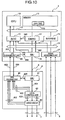
- Fig. 10 is a block diagram showing the second basic structure of the vehicle control apparatus of the present invention.
- the vehicle control apparatus is fundamentally the same as that of the first embodiment.
- a different point resides in that the microcontroller 1 is equipped with an I/O management unit 20.
- the microcontroller 1 may have an A/D converter, a watch dog timer, a general I/O port (GPIO) and the like (not shown).
- GPIO general I/O port
- the I/O management unit 20 manages I/O via serial communications in accordance with the event ID 402 output from the event management unit 40 and a request from CPU 10.
- Fig. 11 is a block diagram of the I/O management unit 20.
- the I/O management unit 20 is constituted of: an event identification circuit 203 for receiving the event ID 402 and identifying which event occurred; a data transfer request register; a control circuit 204 for realizing data transfer between the memory 11 and driver IC 4 by using DMAC 14 and SIU 18, in accordance with the identification result by the event identification circuit 203 and settings in the data transfer request register 206; a transfer address register 207 for loading an address of the memory 11 for a data transfer target; an address buffer 208 for reading the transfer target address and temporarily loading it therein; and a bus controller 205 for controlling data transfer via the peripheral bus 16.
- the transfer address resister 207 can set a plurality of addresses which are assigned to an event notified from the driver IC 4 and one or more data transfer request flags in the data transfer request register 206.
- Application program running on CPU 10 can operate the drive signal 5 of the driver IC 4 only by overwriting the output table 113, and the output process by CPU 10 is not necessary.
- Fig. 12 is a flow chart illustrating the output process to be executed by the I/O management unit 20.
- the event identification circuit 203 identifies an event from the driver IC 4 or CPU detects that the data transfer request flag in the data transfer request register 206 is set (1210), and an address of the transfer address register 207 corresponding to the detected event or data transfer request flag is loaded in the address buffer 208 (1220), and thereafter written in the transfer source address register in DMAC 14 via the bus controller 205 (1230).
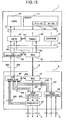
- Fig. 13 is a block diagram showing the third basic structure of the vehicle control apparatus of the present invention.
- the vehicle control apparatus is fundamentally the same as that of the second embodiment shown in Fig. 11.
- a different point resides in that the driver IC 4 has a signal measuring unit 44.
- the microcontroller 1 may have an A/D converter, a watch dog timer, a general I/O port (GPIO), a signal measuring unit and the like (not shown).
- Fig. 14 is a block diagram of the event management unit 40.
- the event management unit 40 is fundamentally the same as that shown in Fig. 3.
- a different point resides in that an event queue 408 is added for queuing the event occurrence signal 442 from the signal measuring unit 44.
- Fig. 15 is a block diagram of the signal measuring unit 44.
- the signal measuring unit 44 is fundamentally the same as the signal measuring unit 17 shown in Fig. 6. A different point resides in that the signal measuring unit outputs an event occurrence signal 442 instead of the interrupt request signal.
- Figs. 16A and 16B are diagrams showing an output table 113 and an input table 114 stored in the memory 11, respectively.
- the I/O management unit 20 writes the control register value in the output table 113 in the control register 4251x
- application software running on CPU 10 can operate the drive signal 5 in the driver IC 4 only by overwriting the output table 113.
- the I/O management unit 20 writes the control register value in the control register 4451x in the input table 114, application software running on CPU 10 can read the measurement result from the input table 114, and the input process by CPU 10 is not necessary.
- the driver IC is equipped with the event management unit, and a copy of the control register of the driver IC is realized on the memory of the microcontroller. Accordingly, application software can perform I/O operations and data read by normal memory access without accessing the driver IC. Since the microcontroller is equipped with the I/O management unit, the input/output process by CPU is not necessary so that a load on CPU can be reduced.
Landscapes
- Engineering & Computer Science (AREA)
- Automation & Control Theory (AREA)
- Human Computer Interaction (AREA)
- Transportation (AREA)
- Mechanical Engineering (AREA)
- Combined Controls Of Internal Combustion Engines (AREA)
- Microcomputers (AREA)
Abstract
Description
- The present invention relates to a vehicle control apparatus for conducting driving, steering and braking of a vehicle through electronic control.
- Electronic control for vehicles have recently expand rapidly aiming at reduction in fuel consumption and exhaust gas and improvement on safety. Controllers are used in a vehicle for controlling an engine, a transmission, a brake and steering, and in addition an air bag, doors, mirrors and the like. A vehicle is equipped with a number of controllers. Basically, these controllers detect the states of control targets from various sensors and instruction information on a drive from operation switches, and in accordance with the state information and instruction information, control actuators such as electromagnetic valves and motors. A signal output from each sensor includes an analog signal and a pulse signal. Controllers are therefore equipped with an A/D converter for converting an analog signal voltage into a digital value and a timer to be used for converting a period or the like of a pulse signal into a digital value. Since actuators such as electromagnetic valves and motors are controlled by pulse signals such as FWM pulse signals, controllers are equipped with a timer to be used for outputting a pulse signal. Controllers are further equipped with a general I/O port for digital signal inputs/outputs in order to fetch information on operation switches and perform simple ON/OFF control for electromagnetic valves. A general controller uses a microcontroller having a central processor unit (CPU), a memory, A/D converters, timers, general I/O ports and the like respectively integrated on the same chip. The advantages of using a microcontroller are mainly reduction in the number of components and corresponding feasibility of substrate designs. However, the A/D converter, timer, general I/O port and the like have each a number of pins to allow a plurality of signals to be connected. There arises therefore an issue that the chip size and package of a microcontroller cannot be made small even if a chip integration degree is improved by advancement of micro patterning.
- To address this issue, a method has been proposed which reduces the number of pins of a microcontroller by connecting the microcontroller, A/D converters and driver ICes through serial communications (refer to "New Serial Microcontroller Links - Micro-Link-Interface And Micro-Second-Channel", SAE-2003-01-0112). According to this method, a driver IC is equipped with a unit for generating a plurality of PWM pulse signals for driving actuators, and ON/OFF commands for the PWM pulse signals generated by using a timer in the microcontroller are transmitted through serial communications to the driver IC which in turn generates the PWM pulse signals.
- With this method, however, since ON/OFF commands for a plurality of PWM pulse signals are time sequentially transferred repetitively through serial communications, the number of signals increases resulting in an issue of a lower resolution of PWM pulses.
- The present invention has been made to address this issue, and an object of the present invention is to provide a vehicle control apparatus and an input/output apparatus for the vehicle control apparatus which can obviate the aforesaid problems of the related art.
- Another object of the present invention is to connect a microcontroller and a driver IC through serial communications without lowering a resolution of PWM pulse signals, and to allow control application software to be developed easily by reducing dependency upon the microcontroller.
- In order to address the above-described issue, the vehicle control apparatus of the present invention comprises an arithmetic processing unit including an arithmetic unit, a storage unit and/or a communication unit, an input/output unit including an signal input unit or a signal output unit and a communication unit, and/or a serial communication line connecting the arithmetic processing unit and/or the input/output unit. The input/output unit is equipped with an event management unit for detecting an event of a signal input or a signal output and notifying the event to the arithmetic processing unit, and/or the arithmetic processing unit is equipped with an input/output management unit for performing data exchange between the signal input unit or the signal output unit and the storage unit via the communication units, in accordance with a request from the arithmetic unit and an event notice from the event management unit. Accordingly, the arithmetic processing unit can exchange data with the input/output unit without using the arithmetic processing unit.
- In the vehicle control apparatus of the present invention, the input/output management unit transfers information externally detected by the signal input unit to the storage unit, or transfers a signal output command stored in the storage unit to the signal output unit, in accordance with the request from the arithmetic unit and the event notice from the event management unit, and the arithmetic unit reads information on the signal input unit stored in the storage unit or writes the signal output command to the signal output unit in the storage unit. Accordingly, the arithmetic unit can exchange data with the input/output unit only by accessing the storage unit.
- In the vehicle control apparatus of the present invention, the arithmetic processing unit includes a data transfer unit, and the input/output management unit supplies the data transfer unit with a command for data transfer between the storage unit and the input/output unit via the communication units. Accordingly, data transfer between the storage unit of the arithmetic processing unit and the input/output unit can be performed automatically.
- An input/output apparatus for a vehicle control apparatus of the present invention, the input/output apparatus being connected to an arithmetic processing unit of a vehicle control apparatus by a serial communication path, comprises a signal input unit or a signal output unit and a communication unit, wherein an event management unit detects an event of a signal input or a signal output to the arithmetic processing unit via the communication unit. Accordingly, a process to be executed by the arithmetic processing unit of the vehicle control apparatus can be synchronized with an event of a signal input or a signal output.
- In the input/output apparatus for a vehicle control apparatus of the present invention, the event management unit notifies the event by outputting an interrupt signal and an event identification signal to the arithmetic processing unit. Accordingly, the arithmetic processing unit of the vehicle control apparatus can execute a process matching the type of each event.
- In the input/output apparatus for a vehicle control apparatus of the present invention, the event management unit sets a priority order for each of the events; and notifies the event in accordance with the priority order. Accordingly, an event occurrence can be notified to the arithmetic processing unit of the vehicle control apparatus in accordance with the priority order of the event.
- In the vehicle control apparatus of the present invention, the arithmetic processing unit and input/output unit are connected by a serial communication line so that the number of pins of the arithmetic processing unit can be reduced. Since the input/output unit is equipped with an event management unit and a copy of a control register in the input/output unit is realized in the memory unit of the arithmetic processing unit, application software can perform I/O operations and data read by normal memory access without accessing the input/output device driver IC. Therefore, the arithmetic processing unit and input/output unit can be connected by the serial communication line without lowering a resolution of PWM pulse signals. Further, control application software can be developed easily. Furthermore, since the arithmetic processing unit is equipped with the input/output management unit, the input/output process by the arithmetic unit is not necessary so that a load on CPU can be reduced.
The above features can be combined in any way partly or as a whole. - Other objects, features and advantages of the invention will become apparent from the following description of the embodiments of the invention taken in conjunction with the accompanying drawings.
-
- Fig. 1 is a block diagram showing a first basic structure of a vehicle control apparatus according to the present invention.
- Fig. 2 is a block diagram of a
drive control unit 42. - Fig. 3 is a block diagram of an
event management unit 40. - Figs. 4A to 4G are timing charts illustrating the operations of the
drive control unit 42 andevent management unit 40. - Figs. 5A to 5G are timing charts illustrating the operations of the
drive control unit 42 andevent management unit 40. - Fig. 6 is a block diagram of a
signal measuring unit 17. - Figs. 7A to 7E are timing charts illustrating the operation of the
signal measuring unit 17. - Fig. 8 is a diagram showing an output table 111 stored in a
memory 11. - Fig. 9 is a flow chart illustrating an
output process 111 to be executed by aCPU 10. - Fig. 10 is a block diagram showing a second basic structure of the vehicle control apparatus according to the present invention.
- Fig. 11 is a block diagram of an I/
O management unit 20. - Fig. 12 is a flow chart illustrating an output process to be executed by the I/
O management unit 20. - Fig. 13 is a block diagram showing a third basic structure of the vehicle control apparatus according to the present invention.
- Fig. 14 is a block diagram of the
event management unit 40. - Fig. 15 is a block diagram of a
signal measuring unit 44. - Figs. 16A and 16B are diagrams showing the output table 113 and an input table 114 stored in the
memory 11, respectively. - Embodiments of a vehicle control apparatus of the present invention will now be described with reference to the accompanying drawings.
- Fig. 1 is a block diagram showing the first basic structure of the vehicle control apparatus of the present invention. The vehicle control apparatus is constituted of a
microcontroller 1 and a driver IC 4. Themicrocontroller 1 and driver IC 4 may be mounted on the same substrate, may be mounted on different substrates and accommodated in the same housing, or may be mounted on different substrates and accommodated in different housings. - The
microcontroller 1 is constituted of a central processor unit (CPU) 10, amemory 11 for storing programs and data, an interrupt control unit (INTC) 13, a direct memory access control unit (DMAC) 14, abus bridge 15, asignal measuring unit 17, a serial interface unit (SIU) 18 and a general I/O port (GPIO) 19.CPU 10,memory 11 andDMAC 14 are connected to aCPU bus 12.INTC 13,DMAC 14,signal measuring unit 17,SIU 18 andGPIO 19 are connected to aperipheral bus 16. TheCPU bus 12 andperipheral bus 16 transfer data via thebus bridge 15. Themicrocontroller 1 may have an A/D convertor, a watch dog timer and the like (not shown). - The interrupt control unit (INTC) 13 receives interrupt requests from the units in the microcontroller and the external driver IC, and outputs an interrupt signal to
CPU 10.INTC 13 has an interrupt factor register (not shown), and upon reception of an interrupt request, sets a corresponding factor flag. By reading this interrupt factor register,CPU 10 can recognize the unit which requested the interrupt. - The direct memory access control unit (DMAC) 14 performs settings for a transfer source address register, a transfer destination address register, a transfer data length and the like (not shown) to execute data transfer between the
memory 11 and each unit in the microcontroller, without involvement ofCPU 10. Upon completion of data transfer,DMAC 14 outputs an interruptrequest signal 141 toCPU 10 to notifyCPU 10 of data transfer completion. - The
signal measuring unit 17 measures the period and frequency of eachpulse signal 6 input from external various sensors, and sequentially writes measurement results in a measurement data register (not shown).CPU 10 can read the measurement results from the measurement data register. Thesignal measuring unit 17 outputs an interruptrequest signal 171 when the measurement data register is updated, to notifyCPU 10 of measurement data update. - The serial interface unit (SIU) 18 performs data transmission/reception to/from the external driver IC and the like via a
serial line 3 and has a status register and the like including a transmission data register, a reception data register, a transmission completion flag, and a reception completion flag (not shown). Upon completion of data transmission or data reception,SIU 18 outputs an interruptrequest signal 181 to notifyCPU 10 of data transmission or reception completion.SIU 18 can cooperate withDMAC 14. For data transmission,SIU 18 outputs aDMA request signal 182 toDMAC 14 when the transmission data register becomes empty, andDMAC 14 executes data transfer from the memory to the transmission data register. For data reception,SIU 18 outputs theDMA request signal 182 toDMAC 14 when reception data is loaded in the reception data register, andDMAC 14 executes data transfer from the reception data register inSIU 18 to the memory. - The general I/O port (GPIO) 19 reads the states (High or Low) of one or more digital input signals in a register and writes the states (High or Low) of one or more digital output signals in a register.
- The driver IC 4 is constituted of an
event management unit 40, a serial interface unit (SIU) 41, adrive control unit 42 and adrive circuit 43. - The
event management unit 40 receives anevent notice 422 from thedrive control unit 42 and anevent notice 432 from thedrive circuit 43, and outputs an interruptsignal 401 and anevent ID 402 to themicrocontroller 1. -
SIU 41 is connected toSIU 18 of themicrocontroller 1 via theserial signal line 3 to perform serial communication between themicrocontroller 1 and driver IC 4. - The drive control unit 2 generates a
control pulse signal 423 for controlling thedrive circuit 43. - The
drive circuit 43 generates adrive signal 5 for a control target actuator. - Fig. 2 is a block diagram of the drive control unit.
- The
drive control unit 42 has three drive control circuits (425a, 425b, 425c) if there are three channels of thecontrol pulse signal 423. The drive control circuit 425s has acontrol register 4251a, atimer 4252a and a compare/match circuit 4253a. Thecontrol register 4251a is constituted of an output enable flag (EN), a mode flag (MD), an event notice enable flag (EE), an output compare 1 (T1) and an output compare 2 (T2). EN controls start/stop of thetimer 4252a, "0" for stop and "1" for start. MD sets an operation mode of thetimer 4252a, "0" for a single mode and "1" for a continuous mode. EE sets whether theevent occurrence signal 422 is output or not when a compare/match occurs, "0" for no-output and "1" for output. T1 and T2 set a fall time and a rise time of thecontrol pulse signal 423 to be output. In this embodiment, T1 sets the fall time and T2 sets the rise time. - The
timer 4252a generates a reference time to be used for generating thecontrol pulse signal 423. If MD in thecontrol register 4251a is set to the single mode, the timer starts incrementing a timer value when "1" is set to EN in the register, and when the timer value becomes coincident with T2, the timer value is cleared to "0" to stop incrementing. If MD in thecontrol register 4251a is set to the continuous mode, the timer starts incrementing a timer value when "1" is set to EN in the register, and when the timer value becomes coincident with T2, the timer value is cleared to "0" to thereafter resume incrementing repetitively. - The compare/
match circuit 4253a compares the timer value of thetimer 4252a with the values T1 and T2 in thecontrol register 4251a, changes thecontrol pulse signal 423 from High to Low when the timer value becomes coincident with T1, and changes thecontrol pulse signal 423 from Low to High when the timer value becomes coincident with T2. - Fig. 3 is a block diagram of the
event management unit 40. - The
event management unit 40 is equipped with: a priority order setting table 406 for setting a priority order in notifying the microcontroller of event notices from thedrive control unit 42 and drivecircuit 43; an eventnotice arbitration unit 407 for arbitrating the event notices from thedrive control unit 42 and drivecircuit 43 in accordance with the priority order setting table, and notifying themicrocontroller 1 of an event notice; andevent queues drive control unit 42 and drivecircuit 43. - The priority order setting table 406 can be set by
CPU 10 of themicrocontroller 1 via serial communications. - The event
notice arbitration unit 407 refers to the priority order setting table 406 to select an event having a highest priority order among events queued in theevent queues request signal 401 andevent ID 402 to themicrocontroller 1. In themicrocontroller 1,INTC 13 receives the interruptrequest signal 401, andGPIO 19 receives theevent ID 402. The microcontroller outputs an eventnotice reception signal 191 viaGPIO 19. Upon reception of the eventnotice reception signal 191, the eventnotice arbitration unit 407 arbitrates new event notices. - Each of the
event queues drive control unit 42 and drivecircuit 43. - Figs. 4A to 4G are timing chart illustrating the operations of the
drive control unit 42 andevent management unit 40. It is assumed herein that the operation mode of thetimer 4252a is the single mode. - The
timer 4252a starts incrementing a timer value when "1" is set to EN in thecontrol register 4251a, and when the timer value becomes coincident with T2, the timer value is cleared to "0" to stop incrementing. - The compare/
match circuit 4253a compares the timer value of thetimer 4252a with the values T1 and T2 in thecontrol register 4251a, changes thecontrol pulse signal 423 from High to Low when the timer value becomes coincident with T1, changes thecontrol pulse signal 423 from Low to High and outputs theevent occurrence signal 422 when the timer value becomes coincident with T2. - The
event queue 403 queues each occurred event. - The event
notice arbitration unit 407 selects an event from theevent queue 403, and outputs the interruptrequest signal 401 andevent ID 402 to themicrocontroller 1. In themicrocontroller 1,INTC 13 receives the interruptrequest signal 401, andGPIO 19 receives theevent ID 402. - Upon reception of the interrupt
request signal 401,INTC 13 issues an interrupt toCPU 10, andCPU 10 outputs the eventnotice reception signal 191 viaGPIO 19 in the interrupt process. Upon reception of the eventnotice reception signal 191, the eventnotice arbitration unit 407 completes the output of the interruptrequest signal 401 andevent ID 402, and arbitrates new event notices. - Figs. 5A to 5G are timing charts illustrating the operations of the
drive control unit 42 andevent management unit 40. It is assumed herein that the operation mode of thetimer 4252a is the continuous mode. The fundamental operation is the same as that of the single mode shown in Figs. 4A to 4G. A different point resides in that when the timer value of thetimer 4252a becomes coincident with the value T2, the timer value is cleared to "0" to resume incrementing. - Fig. 6 is a block diagram of the
signal measuring unit 17 of themicrocontroller 1. - The
signal measuring unit 17 has three signal measuring circuits (175a, 175b and 175c) if there are three channels of thepulse signal 6 from the sensors and the like. - The
signal measuring circuit 175a has acontrol register 1751a, atimer 1752a and aninput capture circuit 1753a. Thecontrol register 1751a is constituted of a measuring enable flag (EN), a mode flag (MD), an event notice enable flag (EE), an input capture 1 (T1) and an input capture 2 (T2). EN controls execution/no-execution of signal measuring, "0" for execution and "1" for no-execution. MD sets an operation mode of thetimer 1752a, "0" for a single mode and "1" for a free-run mode. EE sets whether the interruptrequest signal 171 is output or not during input capture, "0" for no-output and "1" for output. T1 stores a timer value at the fall of thepulse signal 6, and T2 stores a timer value at the rise of thepulse signal 6. - If EN in the
control register 1751a is set to the execution and MD is set to the single mode, theinput capture circuit 1753a stores the timer value at the fall of thepulse signal 6 in T1, stores the timer value at the rise of the pulse signal in T2, and thereafter clears the timer value to "0" to resume incrementing repetitively. If EN in thecontrol register 1751a is set to the execution and MD is set to the free-run mode, theinput capture circuit 1753a stores the timer value at the fall of thepulse signal 6 in T1 and stores the timer value at the rise of the pulse signal in T2. This operation is repetitively performed. In the free-run mode, the timer value is not cleared to "0" until thetimer 1752a overflows. If EE is set to the interrupt request signal output, theinput capture circuit 1753a outputs the interruptrequest signal 171 when the timer value at the rise of thepulse signal 6 is stored in T2. - Figs. 7A to 7E are timing charts illustrating the
signal measuring unit 17. It is herein assumed that the operation mode is the single mode. - The
input capture circuit 1753a stores the timer value at the fall of thepulse signal 6 in T1, stores the timer value at the rise of thepulse signal 6 in T2, and thereafter clears the timer value of thetimer 1752a to "0" to resume incrementing. The input capture circuit outputs the interrupt request signal 171 at the rise of thepulse signal 6. - Fig. 8 is a diagram showing an output table 113 stored in the
memory 11. - The output table 113 is a copy of the control register 4251x (x is 1, 2, ..., n) in the
drive control unit 42 of the driver IC 4. In anoutput process 111, control register values in the output table 113 are written in the control register 4251x, so that application software running onCPU 10 can operate thedrive signal 5 of the driver IC simply by overwriting the output table 113. - Fig. 9 is a flow chart illustrating the
output process 111 to be executed byCPU 10. - In the
output process 111, a control register value of the target channel is first set to the output table 113 (910), and then the transfer source address register, transfer destination address register, transfer data length and the like inDMAC 14 are set to DMA transfer the control register value of the target channel from thememory 11 to the transmission data register in SIU 18 (920), and DMA transfer ofDMAC 14 is activated (930). Thereafter, the transfer completion flag ofDMAC 14 and the serial transmission completion flag ofSIU 18 are polled to terminate the process after completion of DMA transfer and serial transmission (940, 950). - In the first basic structure described above, the
output process 111 executed byCPU 10 performs input/output management of data between thedrive control unit 42 as a signal input unit or signal output unit and thememory 11 as a storage unit. - Fig. 10 is a block diagram showing the second basic structure of the vehicle control apparatus of the present invention. The vehicle control apparatus is fundamentally the same as that of the first embodiment. A different point resides in that the
microcontroller 1 is equipped with an I/O management unit 20. Themicrocontroller 1 may have an A/D converter, a watch dog timer, a general I/O port (GPIO) and the like (not shown). - The I/
O management unit 20 manages I/O via serial communications in accordance with theevent ID 402 output from theevent management unit 40 and a request fromCPU 10. - Fig. 11 is a block diagram of the I/
O management unit 20. - The I/
O management unit 20 is constituted of: anevent identification circuit 203 for receiving theevent ID 402 and identifying which event occurred; a data transfer request register; acontrol circuit 204 for realizing data transfer between thememory 11 and driver IC 4 by usingDMAC 14 andSIU 18, in accordance with the identification result by theevent identification circuit 203 and settings in the datatransfer request register 206; a transfer address register 207 for loading an address of thememory 11 for a data transfer target; anaddress buffer 208 for reading the transfer target address and temporarily loading it therein; and abus controller 205 for controlling data transfer via theperipheral bus 16. - The
transfer address resister 207 can set a plurality of addresses which are assigned to an event notified from the driver IC 4 and one or more data transfer request flags in the datatransfer request register 206. - If the
event identification circuit 203 identifies an event from the driver IC 4 or ifCPU 10 sets the data transfer request flag in the datatransfer request register 206, thecontrol circuit 204 stores the address in the transfer address register corresponding to the event or data transfer request flag in the address buffer, writes it in the transfer source address register inDMAC 14 via thebus controller 205, activates DMA transfer byDMAC 14, and writes the control register value of the target channel in the output table 113 in the memory into the control register 4251x (x = 1, 2, ..., n) in thedrive control unit 42 of the driver IC 4 through data transfer viaSIU 18. Application program running onCPU 10 can operate thedrive signal 5 of the driver IC 4 only by overwriting the output table 113, and the output process byCPU 10 is not necessary. - Fig. 12 is a flow chart illustrating the output process to be executed by the I/
O management unit 20. - First, the
event identification circuit 203 identifies an event from the driver IC 4 or CPU detects that the data transfer request flag in the datatransfer request register 206 is set (1210), and an address of the transfer address register 207 corresponding to the detected event or data transfer request flag is loaded in the address buffer 208 (1220), and thereafter written in the transfer source address register inDMAC 14 via the bus controller 205 (1230). DMA transfer ofDMAC 14 is activated to write the control register value of the target channel in the output table 113 in thememory 11, in the control register 4251x (x = 1, 2, ..., n) in thedrive controller 42 of the driver IC 4 (1240). Thereafter, the transfer completion flag ofDMAC 14 and the serial transmission completion flag ofSIU 18 are polled to terminate the process after completion of DMA transfer and serial transmission (1250, 1260). - Fig. 13 is a block diagram showing the third basic structure of the vehicle control apparatus of the present invention. The vehicle control apparatus is fundamentally the same as that of the second embodiment shown in Fig. 11. A different point resides in that the driver IC 4 has a
signal measuring unit 44. Themicrocontroller 1 may have an A/D converter, a watch dog timer, a general I/O port (GPIO), a signal measuring unit and the like (not shown). - Fig. 14 is a block diagram of the
event management unit 40. Theevent management unit 40 is fundamentally the same as that shown in Fig. 3. A different point resides in that anevent queue 408 is added for queuing the event occurrence signal 442 from thesignal measuring unit 44. - Fig. 15 is a block diagram of the
signal measuring unit 44. Thesignal measuring unit 44 is fundamentally the same as thesignal measuring unit 17 shown in Fig. 6. A different point resides in that the signal measuring unit outputs anevent occurrence signal 442 instead of the interrupt request signal. - Figs. 16A and 16B are diagrams showing an output table 113 and an input table 114 stored in the
memory 11, respectively. - The output table 113 is a copy of the control register 4251x (x = 1, 2, ..., n) in the
drive control unit 42 of the driver IC 4. As the I/O management unit 20 writes the control register value in the output table 113 in the control register 4251x, application software running onCPU 10 can operate thedrive signal 5 in the driver IC 4 only by overwriting the output table 113. - The input table 114 is a copy of the control register 4451x (x = 1, 2, ..., n) in the
signal measuring unit 44 of the driver IC 4. As the I/O management unit 20 writes the control register value in the control register 4451x in the input table 114, application software running onCPU 10 can read the measurement result from the input table 114, and the input process byCPU 10 is not necessary. - According to the embodiments described above, in the vehicle control apparatus having the microcontroller and driver IC interconnected by a serial communication line, the driver IC is equipped with the event management unit, and a copy of the control register of the driver IC is realized on the memory of the microcontroller. Accordingly, application software can perform I/O operations and data read by normal memory access without accessing the driver IC. Since the microcontroller is equipped with the I/O management unit, the input/output process by CPU is not necessary so that a load on CPU can be reduced.
- It should be further understood by those skilled in the art that although the foregoing description has been made on embodiments of the invention, the invention is not limited thereto and various changes and modifications may be made without departing from the spirit of the invention and the scope of the appended claims.
- The above features and embodiments may be combined in any way partly or as a whole.
Claims (6)
- A vehicle control apparatus comprising:an arithmetic processing unit (1) including an arithmetic unit, a storage unit and a communication unit;an input/output unit (4) including a signal input unit or a signal output unit and a communication unit; anda serial communication line (3) connecting said arithmetic processing unit and said input/output unit,wherein:said input/output unit is equipped with an event management unit (40) for detecting an event of a signal input or a signal output and notifying said event to said arithmetic processing unit; andsaid arithmetic processing unit is equipped with an input/output management unit (13)~(15) for performing data exchange between said signal input unit or said signal output unit and said storage unit via said communication units, in accordance with a request from said arithmetic unit and an event notice from said event management unit.
- The vehicle control apparatus according to claim 1, wherein:said input/output management unit transfers information externally detected by said signal input unit to said storage unit, or transfers a signal output command stored in said storage unit to said signal output unit, in accordance with the request from said arithmetic unit and the event notice from said event management unit; andsaid arithmetic unit reads information on said signal input unit stored in said storage unit or writes the signal output command to said signal output unit in said storage unit.
- The vehicle control apparatus according to claim 1 or 2, wherein:said arithmetic processing unit includes a data transfer unit; andsaid input/output management unit supplies said data transfer unit with a command for data transfer between said storage unit and said input/output unit via said communication units.
- An input/output apparatus (4) for a vehicle control apparatus, the input/output apparatus connected to an arithmetic processing unit (1) of a vehicle control apparatus by a serial communication path (3), comprising:a signal input unit or a signal output unit; a communication unit (41); andan event management unit (40),wherein said event management unit detects an event of a signal input or a signal output to said arithmetic processing unit via said communication unit.
- The input/output apparatus for a vehicle control apparatus according to claim 4, wherein said event management unit notifies said event by outputting an interrupt signal and an event identification signal to said arithmetic processing unit.
- The input/output apparatus for a vehicle control apparatus according to claim 4 or 5, wherein said event management unit sets a priority order for each of said events, and notifies said event in accordance with said priority order.
Applications Claiming Priority (1)
| Application Number | Priority Date | Filing Date | Title |
|---|---|---|---|
| JP2006018016A JP4828947B2 (en) | 2006-01-26 | 2006-01-26 | Vehicle control device input/output device |
Publications (2)
| Publication Number | Publication Date |
|---|---|
| EP1813494A1 true EP1813494A1 (en) | 2007-08-01 |
| EP1813494B1 EP1813494B1 (en) | 2009-09-23 |
Family
ID=37872201
Family Applications (1)
| Application Number | Title | Priority Date | Filing Date |
|---|---|---|---|
| EP07000894A Ceased EP1813494B1 (en) | 2006-01-26 | 2007-01-17 | Vehicle control apparatus having event management unit |
Country Status (4)
| Country | Link |
|---|---|
| US (1) | US7769511B2 (en) |
| EP (1) | EP1813494B1 (en) |
| JP (1) | JP4828947B2 (en) |
| DE (1) | DE602007002504D1 (en) |
Cited By (2)
| Publication number | Priority date | Publication date | Assignee | Title |
|---|---|---|---|---|
| WO2009021819A1 (en) * | 2007-08-16 | 2009-02-19 | Robert Bosch Gmbh | Companion chip for a microcontroller |
| WO2009021816A1 (en) * | 2007-08-16 | 2009-02-19 | Robert Bosch Gmbh | Communication method and interface between a companion chip and a microcontroller |
Families Citing this family (2)
| Publication number | Priority date | Publication date | Assignee | Title |
|---|---|---|---|---|
| JP5149044B2 (en) * | 2008-03-11 | 2013-02-20 | 矢崎総業株式会社 | Electronic control device and vehicle system |
| JP2017037505A (en) * | 2015-08-11 | 2017-02-16 | ルネサスエレクトロニクス株式会社 | Semiconductor device |
Citations (8)
| Publication number | Priority date | Publication date | Assignee | Title |
|---|---|---|---|---|
| US4760275A (en) * | 1986-04-09 | 1988-07-26 | Nippondenso Co., Ltd. | Communication system for vehicle |
| US5719771A (en) * | 1993-02-24 | 1998-02-17 | Amsc Subsidiary Corporation | System for mapping occurrences of conditions in a transport route |
| US20020035650A1 (en) * | 2000-09-19 | 2002-03-21 | Katsuya Nakamoto | Vehicle-mounted electronic control apparatus |
| US20020040261A1 (en) | 2000-09-29 | 2002-04-04 | Katsuya Nakamoto | Vehicle built-in electronic control apparatus |
| US6438462B1 (en) * | 1996-03-26 | 2002-08-20 | Daimlerchrysler Ag | Semiconductor circuit for an electronic unit |
| US20030036843A1 (en) * | 2001-07-25 | 2003-02-20 | Mariko Okude | On-vehicle terminal system |
| US20040215982A1 (en) | 2003-04-22 | 2004-10-28 | Subramanian Senthil K. | System and method for electrical power management in a data processing system |
| US20050190467A1 (en) * | 2004-02-27 | 2005-09-01 | Fuji Jukogyo Kabushiki Kaisha | Control unit and data transmitting method |
Family Cites Families (11)
| Publication number | Priority date | Publication date | Assignee | Title |
|---|---|---|---|---|
| US470275A (en) * | 1892-03-08 | wooster | ||
| JPH077957B2 (en) * | 1989-10-13 | 1995-01-30 | トヨタ自動車株式会社 | In-vehicle communication control device |
| JPH04182803A (en) * | 1990-11-19 | 1992-06-30 | Nissan Motor Co Ltd | Computer for event driving type vehicle control |
| JP3517951B2 (en) * | 1994-05-18 | 2004-04-12 | 株式会社デンソー | Control device for internal combustion engine for vehicle |
| IL117792A (en) * | 1995-05-08 | 2003-10-31 | Rafael Armament Dev Authority | Autonomous command and control unit for mobile platform |
| JP3385162B2 (en) * | 1996-07-08 | 2003-03-10 | 矢崎総業株式会社 | Vehicle multiplex transmission equipment |
| JPH1029477A (en) * | 1996-07-17 | 1998-02-03 | Toyota Motor Corp | Electronic control device and control method thereof |
| JP3566846B2 (en) * | 1997-12-24 | 2004-09-15 | 古河電気工業株式会社 | Multiplex communication method |
| US6374161B1 (en) * | 1999-04-26 | 2002-04-16 | Denso Corporation | Automobile control system and method capable of revising control data transmission function |
| US6981176B2 (en) * | 1999-05-10 | 2005-12-27 | Delphi Technologies, Inc. | Secured microcontroller architecture |
| JP2003063327A (en) * | 2001-08-24 | 2003-03-05 | Nissan Motor Co Ltd | Vehicle electronic control unit |
-
2006
- 2006-01-26 JP JP2006018016A patent/JP4828947B2/en not_active Expired - Fee Related
-
2007
- 2007-01-17 DE DE602007002504T patent/DE602007002504D1/en active Active
- 2007-01-17 EP EP07000894A patent/EP1813494B1/en not_active Ceased
- 2007-01-19 US US11/655,127 patent/US7769511B2/en not_active Expired - Fee Related
Patent Citations (8)
| Publication number | Priority date | Publication date | Assignee | Title |
|---|---|---|---|---|
| US4760275A (en) * | 1986-04-09 | 1988-07-26 | Nippondenso Co., Ltd. | Communication system for vehicle |
| US5719771A (en) * | 1993-02-24 | 1998-02-17 | Amsc Subsidiary Corporation | System for mapping occurrences of conditions in a transport route |
| US6438462B1 (en) * | 1996-03-26 | 2002-08-20 | Daimlerchrysler Ag | Semiconductor circuit for an electronic unit |
| US20020035650A1 (en) * | 2000-09-19 | 2002-03-21 | Katsuya Nakamoto | Vehicle-mounted electronic control apparatus |
| US20020040261A1 (en) | 2000-09-29 | 2002-04-04 | Katsuya Nakamoto | Vehicle built-in electronic control apparatus |
| US20030036843A1 (en) * | 2001-07-25 | 2003-02-20 | Mariko Okude | On-vehicle terminal system |
| US20040215982A1 (en) | 2003-04-22 | 2004-10-28 | Subramanian Senthil K. | System and method for electrical power management in a data processing system |
| US20050190467A1 (en) * | 2004-02-27 | 2005-09-01 | Fuji Jukogyo Kabushiki Kaisha | Control unit and data transmitting method |
Cited By (3)
| Publication number | Priority date | Publication date | Assignee | Title |
|---|---|---|---|---|
| WO2009021819A1 (en) * | 2007-08-16 | 2009-02-19 | Robert Bosch Gmbh | Companion chip for a microcontroller |
| WO2009021816A1 (en) * | 2007-08-16 | 2009-02-19 | Robert Bosch Gmbh | Communication method and interface between a companion chip and a microcontroller |
| US8312251B2 (en) | 2007-08-16 | 2012-11-13 | Robert Bosch Gmbh | Companion chip for a microcontroller with global time management module ensuring consistency and FIFO module for internal and external data transfer |
Also Published As
| Publication number | Publication date |
|---|---|
| US7769511B2 (en) | 2010-08-03 |
| DE602007002504D1 (en) | 2009-11-05 |
| EP1813494B1 (en) | 2009-09-23 |
| JP4828947B2 (en) | 2011-11-30 |
| US20070174373A1 (en) | 2007-07-26 |
| JP2007196859A (en) | 2007-08-09 |
Similar Documents
| Publication | Publication Date | Title |
|---|---|---|
| US5784647A (en) | Interface for fetching highest priority demand from priority queue, predicting completion within time limitation then issuing demand, else adding demand to pending queue or canceling | |
| US10198382B2 (en) | 12C bus controller slave address register and command FIFO buffer | |
| US7650274B2 (en) | Microcomputer logic development system | |
| US9594720B2 (en) | Interface between a bus and a inter-thread interconnect | |
| US20050172059A1 (en) | Data communication system and controller | |
| US5475850A (en) | Multistate microprocessor bus arbitration signals | |
| US20030115491A1 (en) | Apparatus and method for performing power management functions | |
| WO1999027434A1 (en) | Using firmware to enhance the functionality of a controller | |
| US7769511B2 (en) | Vehicle control apparatus having event management unit | |
| US7539610B2 (en) | Microcomputer logic development | |
| CN102859488B (en) | Coprocessor with task flow control | |
| US20090177807A1 (en) | Reset method for application specific integrated circuits (asic) | |
| EP1434137A1 (en) | Bus architecture with primary bus and secondary bus for microprocessor systems | |
| JP4549396B2 (en) | Vehicle control device | |
| US5949980A (en) | Bus interface unit for preventing deadlock | |
| JP4327081B2 (en) | Memory access control circuit | |
| US20060179172A1 (en) | Method and system for reducing power consumption of a direct memory access controller | |
| US20110060852A1 (en) | Computer system and data transfer method therein | |
| US20110055446A1 (en) | Semiconductor integrated circuit device | |
| JPH08314850A (en) | Computer system bus bridge | |
| JPH05282243A (en) | Bus master device and electronic equipment using the same | |
| EP1593040A1 (en) | Asynchronous communications technique | |
| JP3467188B2 (en) | Multiplexing bus order guarantee system. | |
| JP2768352B2 (en) | Graphic drawing processing system | |
| JP6929074B2 (en) | Information processing device and its control method |
Legal Events
| Date | Code | Title | Description |
|---|---|---|---|
| PUAI | Public reference made under article 153(3) epc to a published international application that has entered the european phase |
Free format text: ORIGINAL CODE: 0009012 |
|
| AK | Designated contracting states |
Kind code of ref document: A1 Designated state(s): AT BE BG CH CY CZ DE DK EE ES FI FR GB GR HU IE IS IT LI LT LU LV MC NL PL PT RO SE SI SK TR |
|
| AX | Request for extension of the european patent |
Extension state: AL BA HR MK YU |
|
| 17P | Request for examination filed |
Effective date: 20080201 |
|
| AKX | Designation fees paid |
Designated state(s): DE |
|
| 17Q | First examination report despatched |
Effective date: 20080905 |
|
| GRAP | Despatch of communication of intention to grant a patent |
Free format text: ORIGINAL CODE: EPIDOSNIGR1 |
|
| GRAS | Grant fee paid |
Free format text: ORIGINAL CODE: EPIDOSNIGR3 |
|
| GRAA | (expected) grant |
Free format text: ORIGINAL CODE: 0009210 |
|
| AK | Designated contracting states |
Kind code of ref document: B1 Designated state(s): DE |
|
| REF | Corresponds to: |
Ref document number: 602007002504 Country of ref document: DE Date of ref document: 20091105 Kind code of ref document: P |
|
| PLBE | No opposition filed within time limit |
Free format text: ORIGINAL CODE: 0009261 |
|
| STAA | Information on the status of an ep patent application or granted ep patent |
Free format text: STATUS: NO OPPOSITION FILED WITHIN TIME LIMIT |
|
| 26N | No opposition filed |
Effective date: 20100624 |
|
| PGFP | Annual fee paid to national office [announced via postgrant information from national office to epo] |
Ref country code: DE Payment date: 20150113 Year of fee payment: 9 |
|
| REG | Reference to a national code |
Ref country code: DE Ref legal event code: R119 Ref document number: 602007002504 Country of ref document: DE |
|
| PG25 | Lapsed in a contracting state [announced via postgrant information from national office to epo] |
Ref country code: DE Free format text: LAPSE BECAUSE OF NON-PAYMENT OF DUE FEES Effective date: 20160802 |