EP1811620A2 - Surface emitting type semiconductor laser - Google Patents
Surface emitting type semiconductor laser Download PDFInfo
- Publication number
- EP1811620A2 EP1811620A2 EP07000563A EP07000563A EP1811620A2 EP 1811620 A2 EP1811620 A2 EP 1811620A2 EP 07000563 A EP07000563 A EP 07000563A EP 07000563 A EP07000563 A EP 07000563A EP 1811620 A2 EP1811620 A2 EP 1811620A2
- Authority
- EP
- European Patent Office
- Prior art keywords
- mirror
- laser
- ses
- film
- heat radiation
- Prior art date
- Legal status (The legal status is an assumption and is not a legal conclusion. Google has not performed a legal analysis and makes no representation as to the accuracy of the status listed.)
- Withdrawn
Links
Images




Classifications
-
- H—ELECTRICITY
- H01—ELECTRIC ELEMENTS
- H01S—DEVICES USING THE PROCESS OF LIGHT AMPLIFICATION BY STIMULATED EMISSION OF RADIATION [LASER] TO AMPLIFY OR GENERATE LIGHT; DEVICES USING STIMULATED EMISSION OF ELECTROMAGNETIC RADIATION IN WAVE RANGES OTHER THAN OPTICAL
- H01S5/00—Semiconductor lasers
- H01S5/10—Construction or shape of the optical resonator, e.g. extended or external cavity, coupled cavities, bent-guide, varying width, thickness or composition of the active region
- H01S5/18—Surface-emitting [SE] lasers, e.g. having both horizontal and vertical cavities
- H01S5/183—Surface-emitting [SE] lasers, e.g. having both horizontal and vertical cavities having only vertical cavities, e.g. vertical cavity surface-emitting lasers [VCSEL]
- H01S5/18386—Details of the emission surface for influencing the near- or far-field, e.g. a grating on the surface
- H01S5/18391—Aperiodic structuring to influence the near- or far-field distribution
-
- H—ELECTRICITY
- H01—ELECTRIC ELEMENTS
- H01S—DEVICES USING THE PROCESS OF LIGHT AMPLIFICATION BY STIMULATED EMISSION OF RADIATION [LASER] TO AMPLIFY OR GENERATE LIGHT; DEVICES USING STIMULATED EMISSION OF ELECTROMAGNETIC RADIATION IN WAVE RANGES OTHER THAN OPTICAL
- H01S5/00—Semiconductor lasers
- H01S5/10—Construction or shape of the optical resonator, e.g. extended or external cavity, coupled cavities, bent-guide, varying width, thickness or composition of the active region
- H01S5/18—Surface-emitting [SE] lasers, e.g. having both horizontal and vertical cavities
- H01S5/183—Surface-emitting [SE] lasers, e.g. having both horizontal and vertical cavities having only vertical cavities, e.g. vertical cavity surface-emitting lasers [VCSEL]
-
- B—PERFORMING OPERATIONS; TRANSPORTING
- B82—NANOTECHNOLOGY
- B82Y—SPECIFIC USES OR APPLICATIONS OF NANOSTRUCTURES; MEASUREMENT OR ANALYSIS OF NANOSTRUCTURES; MANUFACTURE OR TREATMENT OF NANOSTRUCTURES
- B82Y20/00—Nanooptics, e.g. quantum optics or photonic crystals
-
- H—ELECTRICITY
- H01—ELECTRIC ELEMENTS
- H01S—DEVICES USING THE PROCESS OF LIGHT AMPLIFICATION BY STIMULATED EMISSION OF RADIATION [LASER] TO AMPLIFY OR GENERATE LIGHT; DEVICES USING STIMULATED EMISSION OF ELECTROMAGNETIC RADIATION IN WAVE RANGES OTHER THAN OPTICAL
- H01S5/00—Semiconductor lasers
- H01S5/04—Processes or apparatus for excitation, e.g. pumping, e.g. by electron beams
- H01S5/042—Electrical excitation ; Circuits therefor
- H01S5/0425—Electrodes, e.g. characterised by the structure
- H01S5/04252—Electrodes, e.g. characterised by the structure characterised by the material
- H01S5/04253—Electrodes, e.g. characterised by the structure characterised by the material having specific optical properties, e.g. transparent electrodes
-
- H—ELECTRICITY
- H01—ELECTRIC ELEMENTS
- H01S—DEVICES USING THE PROCESS OF LIGHT AMPLIFICATION BY STIMULATED EMISSION OF RADIATION [LASER] TO AMPLIFY OR GENERATE LIGHT; DEVICES USING STIMULATED EMISSION OF ELECTROMAGNETIC RADIATION IN WAVE RANGES OTHER THAN OPTICAL
- H01S2301/00—Functional characteristics
- H01S2301/17—Semiconductor lasers comprising special layers
- H01S2301/176—Specific passivation layers on surfaces other than the emission facet
-
- H—ELECTRICITY
- H01—ELECTRIC ELEMENTS
- H01S—DEVICES USING THE PROCESS OF LIGHT AMPLIFICATION BY STIMULATED EMISSION OF RADIATION [LASER] TO AMPLIFY OR GENERATE LIGHT; DEVICES USING STIMULATED EMISSION OF ELECTROMAGNETIC RADIATION IN WAVE RANGES OTHER THAN OPTICAL
- H01S2301/00—Functional characteristics
- H01S2301/18—Semiconductor lasers with special structural design for influencing the near- or far-field
-
- H—ELECTRICITY
- H01—ELECTRIC ELEMENTS
- H01S—DEVICES USING THE PROCESS OF LIGHT AMPLIFICATION BY STIMULATED EMISSION OF RADIATION [LASER] TO AMPLIFY OR GENERATE LIGHT; DEVICES USING STIMULATED EMISSION OF ELECTROMAGNETIC RADIATION IN WAVE RANGES OTHER THAN OPTICAL
- H01S5/00—Semiconductor lasers
- H01S5/02—Structural details or components not essential to laser action
- H01S5/024—Arrangements for thermal management
-
- H—ELECTRICITY
- H01—ELECTRIC ELEMENTS
- H01S—DEVICES USING THE PROCESS OF LIGHT AMPLIFICATION BY STIMULATED EMISSION OF RADIATION [LASER] TO AMPLIFY OR GENERATE LIGHT; DEVICES USING STIMULATED EMISSION OF ELECTROMAGNETIC RADIATION IN WAVE RANGES OTHER THAN OPTICAL
- H01S5/00—Semiconductor lasers
- H01S5/02—Structural details or components not essential to laser action
- H01S5/024—Arrangements for thermal management
- H01S5/02461—Structure or details of the laser chip to manipulate the heat flow, e.g. passive layers in the chip with a low heat conductivity
-
- H—ELECTRICITY
- H01—ELECTRIC ELEMENTS
- H01S—DEVICES USING THE PROCESS OF LIGHT AMPLIFICATION BY STIMULATED EMISSION OF RADIATION [LASER] TO AMPLIFY OR GENERATE LIGHT; DEVICES USING STIMULATED EMISSION OF ELECTROMAGNETIC RADIATION IN WAVE RANGES OTHER THAN OPTICAL
- H01S5/00—Semiconductor lasers
- H01S5/04—Processes or apparatus for excitation, e.g. pumping, e.g. by electron beams
- H01S5/042—Electrical excitation ; Circuits therefor
- H01S5/0425—Electrodes, e.g. characterised by the structure
- H01S5/04254—Electrodes, e.g. characterised by the structure characterised by the shape
-
- H—ELECTRICITY
- H01—ELECTRIC ELEMENTS
- H01S—DEVICES USING THE PROCESS OF LIGHT AMPLIFICATION BY STIMULATED EMISSION OF RADIATION [LASER] TO AMPLIFY OR GENERATE LIGHT; DEVICES USING STIMULATED EMISSION OF ELECTROMAGNETIC RADIATION IN WAVE RANGES OTHER THAN OPTICAL
- H01S5/00—Semiconductor lasers
- H01S5/10—Construction or shape of the optical resonator, e.g. extended or external cavity, coupled cavities, bent-guide, varying width, thickness or composition of the active region
- H01S5/11—Comprising a photonic bandgap structure
-
- H—ELECTRICITY
- H01—ELECTRIC ELEMENTS
- H01S—DEVICES USING THE PROCESS OF LIGHT AMPLIFICATION BY STIMULATED EMISSION OF RADIATION [LASER] TO AMPLIFY OR GENERATE LIGHT; DEVICES USING STIMULATED EMISSION OF ELECTROMAGNETIC RADIATION IN WAVE RANGES OTHER THAN OPTICAL
- H01S5/00—Semiconductor lasers
- H01S5/10—Construction or shape of the optical resonator, e.g. extended or external cavity, coupled cavities, bent-guide, varying width, thickness or composition of the active region
- H01S5/18—Surface-emitting [SE] lasers, e.g. having both horizontal and vertical cavities
- H01S5/183—Surface-emitting [SE] lasers, e.g. having both horizontal and vertical cavities having only vertical cavities, e.g. vertical cavity surface-emitting lasers [VCSEL]
- H01S5/18305—Surface-emitting [SE] lasers, e.g. having both horizontal and vertical cavities having only vertical cavities, e.g. vertical cavity surface-emitting lasers [VCSEL] with emission through the substrate, i.e. bottom emission
-
- H—ELECTRICITY
- H01—ELECTRIC ELEMENTS
- H01S—DEVICES USING THE PROCESS OF LIGHT AMPLIFICATION BY STIMULATED EMISSION OF RADIATION [LASER] TO AMPLIFY OR GENERATE LIGHT; DEVICES USING STIMULATED EMISSION OF ELECTROMAGNETIC RADIATION IN WAVE RANGES OTHER THAN OPTICAL
- H01S5/00—Semiconductor lasers
- H01S5/10—Construction or shape of the optical resonator, e.g. extended or external cavity, coupled cavities, bent-guide, varying width, thickness or composition of the active region
- H01S5/18—Surface-emitting [SE] lasers, e.g. having both horizontal and vertical cavities
- H01S5/183—Surface-emitting [SE] lasers, e.g. having both horizontal and vertical cavities having only vertical cavities, e.g. vertical cavity surface-emitting lasers [VCSEL]
- H01S5/18308—Surface-emitting [SE] lasers, e.g. having both horizontal and vertical cavities having only vertical cavities, e.g. vertical cavity surface-emitting lasers [VCSEL] having a special structure for lateral current or light confinement
- H01S5/18311—Surface-emitting [SE] lasers, e.g. having both horizontal and vertical cavities having only vertical cavities, e.g. vertical cavity surface-emitting lasers [VCSEL] having a special structure for lateral current or light confinement using selective oxidation
- H01S5/18313—Surface-emitting [SE] lasers, e.g. having both horizontal and vertical cavities having only vertical cavities, e.g. vertical cavity surface-emitting lasers [VCSEL] having a special structure for lateral current or light confinement using selective oxidation by oxidizing at least one of the DBR layers
-
- H—ELECTRICITY
- H01—ELECTRIC ELEMENTS
- H01S—DEVICES USING THE PROCESS OF LIGHT AMPLIFICATION BY STIMULATED EMISSION OF RADIATION [LASER] TO AMPLIFY OR GENERATE LIGHT; DEVICES USING STIMULATED EMISSION OF ELECTROMAGNETIC RADIATION IN WAVE RANGES OTHER THAN OPTICAL
- H01S5/00—Semiconductor lasers
- H01S5/10—Construction or shape of the optical resonator, e.g. extended or external cavity, coupled cavities, bent-guide, varying width, thickness or composition of the active region
- H01S5/18—Surface-emitting [SE] lasers, e.g. having both horizontal and vertical cavities
- H01S5/183—Surface-emitting [SE] lasers, e.g. having both horizontal and vertical cavities having only vertical cavities, e.g. vertical cavity surface-emitting lasers [VCSEL]
- H01S5/18308—Surface-emitting [SE] lasers, e.g. having both horizontal and vertical cavities having only vertical cavities, e.g. vertical cavity surface-emitting lasers [VCSEL] having a special structure for lateral current or light confinement
- H01S5/18322—Position of the structure
- H01S5/18327—Structure being part of a DBR
-
- H—ELECTRICITY
- H01—ELECTRIC ELEMENTS
- H01S—DEVICES USING THE PROCESS OF LIGHT AMPLIFICATION BY STIMULATED EMISSION OF RADIATION [LASER] TO AMPLIFY OR GENERATE LIGHT; DEVICES USING STIMULATED EMISSION OF ELECTROMAGNETIC RADIATION IN WAVE RANGES OTHER THAN OPTICAL
- H01S5/00—Semiconductor lasers
- H01S5/10—Construction or shape of the optical resonator, e.g. extended or external cavity, coupled cavities, bent-guide, varying width, thickness or composition of the active region
- H01S5/18—Surface-emitting [SE] lasers, e.g. having both horizontal and vertical cavities
- H01S5/183—Surface-emitting [SE] lasers, e.g. having both horizontal and vertical cavities having only vertical cavities, e.g. vertical cavity surface-emitting lasers [VCSEL]
- H01S5/18308—Surface-emitting [SE] lasers, e.g. having both horizontal and vertical cavities having only vertical cavities, e.g. vertical cavity surface-emitting lasers [VCSEL] having a special structure for lateral current or light confinement
- H01S5/18338—Non-circular shape of the structure
-
- H—ELECTRICITY
- H01—ELECTRIC ELEMENTS
- H01S—DEVICES USING THE PROCESS OF LIGHT AMPLIFICATION BY STIMULATED EMISSION OF RADIATION [LASER] TO AMPLIFY OR GENERATE LIGHT; DEVICES USING STIMULATED EMISSION OF ELECTROMAGNETIC RADIATION IN WAVE RANGES OTHER THAN OPTICAL
- H01S5/00—Semiconductor lasers
- H01S5/10—Construction or shape of the optical resonator, e.g. extended or external cavity, coupled cavities, bent-guide, varying width, thickness or composition of the active region
- H01S5/18—Surface-emitting [SE] lasers, e.g. having both horizontal and vertical cavities
- H01S5/183—Surface-emitting [SE] lasers, e.g. having both horizontal and vertical cavities having only vertical cavities, e.g. vertical cavity surface-emitting lasers [VCSEL]
- H01S5/18361—Structure of the reflectors, e.g. hybrid mirrors
- H01S5/18369—Structure of the reflectors, e.g. hybrid mirrors based on dielectric materials
-
- H—ELECTRICITY
- H01—ELECTRIC ELEMENTS
- H01S—DEVICES USING THE PROCESS OF LIGHT AMPLIFICATION BY STIMULATED EMISSION OF RADIATION [LASER] TO AMPLIFY OR GENERATE LIGHT; DEVICES USING STIMULATED EMISSION OF ELECTROMAGNETIC RADIATION IN WAVE RANGES OTHER THAN OPTICAL
- H01S5/00—Semiconductor lasers
- H01S5/10—Construction or shape of the optical resonator, e.g. extended or external cavity, coupled cavities, bent-guide, varying width, thickness or composition of the active region
- H01S5/18—Surface-emitting [SE] lasers, e.g. having both horizontal and vertical cavities
- H01S5/183—Surface-emitting [SE] lasers, e.g. having both horizontal and vertical cavities having only vertical cavities, e.g. vertical cavity surface-emitting lasers [VCSEL]
- H01S5/18361—Structure of the reflectors, e.g. hybrid mirrors
- H01S5/18377—Structure of the reflectors, e.g. hybrid mirrors comprising layers of different kind of materials, e.g. combinations of semiconducting with dielectric or metallic layers
-
- H—ELECTRICITY
- H01—ELECTRIC ELEMENTS
- H01S—DEVICES USING THE PROCESS OF LIGHT AMPLIFICATION BY STIMULATED EMISSION OF RADIATION [LASER] TO AMPLIFY OR GENERATE LIGHT; DEVICES USING STIMULATED EMISSION OF ELECTROMAGNETIC RADIATION IN WAVE RANGES OTHER THAN OPTICAL
- H01S5/00—Semiconductor lasers
- H01S5/30—Structure or shape of the active region; Materials used for the active region
- H01S5/34—Structure or shape of the active region; Materials used for the active region comprising quantum well or superlattice structures, e.g. single quantum well [SQW] lasers, multiple quantum well [MQW] lasers or graded index separate confinement heterostructure [GRINSCH] lasers
- H01S5/343—Structure or shape of the active region; Materials used for the active region comprising quantum well or superlattice structures, e.g. single quantum well [SQW] lasers, multiple quantum well [MQW] lasers or graded index separate confinement heterostructure [GRINSCH] lasers in AIIIBV compounds, e.g. AlGaAs-laser, InP-based laser
- H01S5/34313—Structure or shape of the active region; Materials used for the active region comprising quantum well or superlattice structures, e.g. single quantum well [SQW] lasers, multiple quantum well [MQW] lasers or graded index separate confinement heterostructure [GRINSCH] lasers in AIIIBV compounds, e.g. AlGaAs-laser, InP-based laser with a well layer having only As as V-compound, e.g. AlGaAs, InGaAs
- H01S5/3432—Structure or shape of the active region; Materials used for the active region comprising quantum well or superlattice structures, e.g. single quantum well [SQW] lasers, multiple quantum well [MQW] lasers or graded index separate confinement heterostructure [GRINSCH] lasers in AIIIBV compounds, e.g. AlGaAs-laser, InP-based laser with a well layer having only As as V-compound, e.g. AlGaAs, InGaAs the whole junction comprising only (AI)GaAs
Definitions
- the present invention relates to surface-emitting type semiconductor lasers (hereinafter referred to as "SES lasers").
- the number of oscillation modes may be reduced by reducing the volume of each resonator.
- the output of a semiconductor laser increases with an increase in the current value injected, and reaches a maximum value (i.e., a rolloff point) at a certain current value.
- a maximum value i.e., a rolloff point
- the gain spectrum shifts with an increase in the device temperature which is caused by the current injected, and the gain reaches a maximum value at a certain temperature.
- the volume of a resonator is relatively small, the temperature of the device would readily elevate, and its rolloff point is reached at a relatively low current value, such that a sufficient output or current driving range may not be obtained.
- JP-A-2003-86895 describes a method in which a groove reaching the current constricting section is formed around the light emitting section, and an electrode is directly formed over the groove. As a result, the distance between a heat generating section and the electrode is shortened, thereby improving the heat radiation efficiency.
- the SES laser 100 includes a substrate 101, a first mirror 102, an active layer 103 and a second mirror 104.
- the SES laser 100 includes a vertical resonator, and may include a columnar semiconductor deposited body (hereafter referred to as a "columnar section") 120, as shown in FIG. 1.
- the columnar section 120 is composed of a portion of the first mirror 102, the active layer 103 and the second mirror 104.
- the substrate 101 may be formed from a semiconductor substrate, for example, an n-type GaAs substrate.
- the first mirror 102 may be composed of, for example, a distributed reflection type multilayer mirror of 40 pairs of alternately laminated n-type Al 0.9 Ga 0.1 As layers and n-type Al 0.15 Ga 0.85 As layers.
- the active layer 103 may be composed of, for example, GaAs well layers and Al 0.3 Ga 0.7 As barrier layers in which the well layers include a quantum well structure composed of three layers.
- the second mirror layer 104 may be composed of, for example, a distributed reflection type multilayer mirror of 25 pairs of alternately laminated p-type Al 0.9 Ga 0.1 As layers and p-type Al 0.15 Ga 0.85 As layers.
- the second mirror 104 may be made to be p-type by doping, for example, carbon (C), and the first mirror 102 may be made to be n-type by doping, for example, silicon (Si). Accordingly, the p-type second mirror 104, the active layer 103 that is not doped with any impurity, and the n-type first mirror 102 form a pin diode. It is noted that, in the present exemplary embodiment, the columnar section 120 has a circular shape in a plan view in the present embodiment, but may have any other arbitrary shape.
- the second mirror 104 further includes a current constricting section 105 formed in a region near the active layer.
- the current constricting section 105 may be formed from an oxidized constricting section or a proton implanted region.
- the current constricting section 105 may be obtained by oxidizing, for example, an Al x Ga 1-x As (x > 0.95) layer from its side surface, and may have a ring shape in a plan view.
- the second mirror 104 includes a plurality of concave sections 111.
- the convex sections 110 that are defined between concave sections can function as a light confining structure like a known two-dimensional photonic crystal or a Holey fiber. Therefore, the second mirror 104 can have a cyclical refractive index distribution in a plane traversing the direction of laser light emission, due to the concave sections 111.
- the concave sections 111 may be arranged in a triangular lattice configuration or a square lattice configuration.
- the concave sections 111 may have a symmetrical cross-sectional shape, such as, for example, a cylindrical shape, or may have an asymmetrical shape having a taper, such as, for example, a conical shape.
- the concave sections 111 in the present embodiment are triangular, but may be in a polygonal shape other than a triangle or a circular shape, without any particular limitation to the embodiment. Furthermore, if another material is filled in the concave sections 111, a material causing a great refractive index difference with respect to the materials of the second mirror 104 may preferably be selected.
- the light confining region 110 surrounded by the concave sections 111 has a plane configuration that may be a circular shape indicated by a dotted line in FIG. 2, and a diameter B of the light confining region 110 is smaller than an inner diameter A of the current constricting section 105.
- a diameter B of the light confining region 110 is smaller than an inner diameter A of the current constricting section 105.
- the current is confined by the current constricting section 105.
- the amount of generation of Joule heat caused by the resistance can be reduced, and a localized temperature increase can be prevented, such that the amount of current at a rolloff point can be made greater, and a high power output can be obtained. Furthermore, as the current level reaching a rolloff point moves away from the driving current range due to the high power output, such that operations in a wider temperature range can be made possible. In other words, by enlarging the inner diameter A of the current constricting section 105 and at the same time reducing the diameter B of the light confining region 110, the number of oscillation modes can be reduced, and a high power output can be maintained.
- the optical confinement is gradually shifted, and the oscillation mode is transiently determined by a region inside an outer diameter B' but outside the diameter B of the concave sections 111.
- the current confining region and the light confining region only need to have different diameters, and the state of "light confining region surrounded by the concave sections" includes such a transient state, in other words, a state in which the light confining region is defined by a region inside the outer diameter B' of the concave sections 111 but outside the diameter B thereof.
- the diameter B of the light confining region 110 can be appropriately adjusted according to a desired number of modes, a designed wavelength and the like.
- the SES laser 100 further includes a first electrode 114 and a second electrode 116.
- the first electrode 114 and the second electrode 116 are used to drive the SES laser 100.
- the first electrode 114 is formed on a top surface of the second mirror 104.
- the second electrode 116 is formed on a back surface of the semiconductor substrate 101.
- the first electrode 114 may have a plane configuration that is in a ring shape, for example, as shown in FIG. 2. Also, the first electrode 114 may have a linear lead-out section that is lead out from the ring shaped section that is in contact with the top surface of the second mirror 104.
- the second electrode 116 may be composed of, for example, a laminated film of an alloy of gold (Au) and germanium (Ge), and gold (Au).
- the first electrode 114 may be composed of, for example, a laminated film of platinum (Pt), titanium (Ti) and gold (Au). Electrical current is injected in the active layer 103 by the first electrode 114 and the second electrode 116. It is noted that the materials for forming the first electrode 114 and the second electrode 116 are not limited to those described above, and other materials, such as, for example, an alloy of gold (Au) and zinc (Zn) can be used.
- the SES laser 100 defines an emission surface inside the first electrode 114 and can emit light upwardly from the inside of the first electrode 114.
- the second electrode 116 is provided on the back surface of the semiconductor substrate 101, but may be provided on the upper side surface of the first mirror 102.
- the second mirror 104 is formed from a semiconductor multilayer film.
- a part or the entirety of the second mirror 104 may be formed from a dielectric mirror.
- only an upper portion of the second mirror 104 may be composed of a dielectric mirror.
- the concave sections 111 may be formed only in the dielectric mirror, but may penetrate the dielectric mirror.
- FIG. 3 through FIG. 5 are cross-sectional views schematically showing a process for manufacturing the SES laser 100 shown in FIG. 1 and FIG. 2, and correspond to the cross-sectional view shown in FIG. 1, respectively.
- a photoresist is provided in areas other than forming regions where the first electrode 114 and the second electrode 116 are to be formed, and a single layer film or a multilayer film (not shown) of conductive material for electrodes is formed by, for example, a vacuum deposition method. Then portions of the multilayered film other than specified positions (in areas where the photoresist remains) are removed by a known lift-off method, whereby the electrodes are formed in desired regions.
- an annealing treatment is conducted in, for example, a nitrogen atmosphere according to the requirements.
- the temperature of the annealing treatment may be, for example, about 400°C.
- the annealing treatment may be conducted for, for example, about 3 minutes.
- the process described above may be conducted for each of the electrodes, or a plurality of electrodes may be formed at the same time.
- the second electrode 116 may be composed of, for example, a laminated film of an alloy of gold (Au) and germanium (Ge), and gold (Au).
- the first electrode 114 may be composed of, for example, a laminated film of platinum (Pt), titanium (Ti) and gold (Au). It is noted that the materials of the electrodes are not limited to those described above, and other known metals, alloys and laminated films of the aforementioned materials may be used.
- FIG. 6 is a schematic cross-sectional view of an SES laser 200 in accordance with a first modified example.
- the SES laser 200 in accordance with the first modified example is different from the SES laser 100 of the above-described embodiment in that a first electrode 214 is provided near the current constricting section 105.
- the SES laser 200 includes a first columnar section 220 composed of a part of a first mirror 102, an active layer 103 and a second mirror 204.
- the first columnar section 220 includes a second columnar section 230 provided in its upper portion, and a third columnar section 240 provided in its lower portion.
- the second columnar section 230 is formed above the layer where the current constricting section 105 is provided.
- the third columnar section 240 includes a portion of the first mirror 102, the active layer 103, a portion of the second mirror 204, and a current constricting section 105.
- a first electrode 214 is formed on a top surface of the third columnar section 240. Therefore, by improving the conductivity of the topmost layer of the third columnar section 240, current injection can be more uniformly conducted. Accordingly, a GaAs layer that does not contain Al or an AlGaAs layer that hardly contains Al may preferably be formed in a region of the topmost layer of the third columnar section 240 on which the first electrode 214 is to be formed.
- the SES laser 200 can reduce the heat that may be generated by the current flowing through the second mirror 204.
- FIG. 7 is a schematic cross-sectional view of an SES laser 300 in accordance with a second modified example.
- the SES laser 300 in accordance with the second modified example is different from the SES laser 100 of the above-described embodiment in that the SES laser 300 is further equipped with a transparent insulation film 301 and a heat radiation film 302.
- the transparent insulation film 301 transmits light emitted from the SES laser 300 and is composed of insulation material.
- the transparent insulation film 301 may be composed of, for example, a silicon nitride (SiN) thin film.
- the silicon nitride thin film not only has light transmittivity and insulating property, but is also excellent in oxidation resisting property, such that the silicon nitride thin film can prevent oxidation and deterioration of the SES laser 300.
- the heat radiation film 302 transmits light at least in a region above an emission surface of the SES laser 300, and is composed of a material having a high thermal conductivity.
- the heat radiation film 302 may be composed of, for example, silicon carbide (SiC), diamond (diamond-like-carbon), or sapphire.
- the transparent insulation film 301 and the heat radiation film 302 are composed of materials that transmit light emitted from the SES laser 300, such that the SES laser 300 can emit laser light upwardly. Also, the SES laser 300 has improved heat radiation efficiency because it is equipped with the transparent insulation film 301 and the heat radiation film 302. As a result of the above, an elevation of the device temperature by the current injection can be suppressed.
- the steps (1) - (3) for manufacturing the SES laser 100 in accordance with the embodiment described above are conducted, and then a transparent insulation film 301 is formed.
- the transparent insulation film 301 is formed and patterned by known methods.
- a plasma CVD (Chemical Vapor Deposition) method may be used for forming a silicon nitride thin film as the transparent insulation film 301.
- a first electrode 314 and a second electrode 116 are formed by the method described above, and a heat radiation film 302 is formed.
- silicon carbide, diamond, sapphire or the like can be used, as described above.
- a sputter method may be used as the film forming method to form a silicon carbide or sapphire film.
- a CVD method, a sputter method or a thermoelectron impact method may be used as the film forming method to form a diamond film.
- patterning may be conducted by etching or the like to thereby expose a lead-out section of the first electrode 314.
- a lead-out section of the first electrode 314 may be exposed by a lift-off method in which a resist layer is left in advance on an upper surface of the lead-out section, and the resist layer is removed after forming the film.
- the SES laser 300 is manufactured. It is noted that other portions of the structure and manufacturing process for the SES laser 300 in accordance with the second modified example are generally the same as those of the structure and manufacturing process for the SES laser 100 in accordance with the embodiment described above, and therefore their description is omitted.
- FIG. 8 is a schematic cross-sectional view of an SES laser 400 in accordance with a third modified example.
- the SES laser 400 in accordance with the third modified example is different from the SES laser 100 of the above-described embodiment in that the SES laser 400 is further equipped with a dielectric layer 405 above a second mirror 404.
- the dielectric layer 405 may be composed of alternately laminated layers having different refractive indexes, and can function as a mirror like the second mirror 404.
- the dielectric layer 405 has a plane configuration that is in, for example, a circular shape having a smaller diameter than that of the second mirror 404, but may not be limited to this particular embodiment.
- concave sections 411 may be formed in the top surface of the second mirror 404.
- the concave sections 411 may be formed only in the dielectric layer 405, or the concave sections 411 may be formed in a manner to penetrate the dielectric layer 405 to the second mirror 404. Also, a portion of the dielectric layer 405 may extend into the concave section 411. As a result, light confinement occurs by the difference between the refractive index of the second mirror 404 and the refractive index of the dielectric layer 405 embedded in the concave sections 411, and the number of oscillation modes is determined by a diameter B inside of the concave sections 411.
- the dielectric layer 405 that can function as a mirror above the second mirror 404 the film thickness of the second mirror 404 can be made smaller.
- the concave sections 411 can be formed near the active layer 103, such that the oscillation mode can be more effectively controlled.
- a first electrode 414 is formed on the top surface of the second mirror 404.
- the first electrode 414 may be formed around the dielectric layer 405.
- the film thickness of the second mirror 404 can be made smaller, as described above, and the distance in which current flows through the second mirror 404 can be made shorter. As a result, the resistance can be lowered, and heat generation can be reduced.
- the dielectric layer 405 may be formed with Ta 2 O 3 , TiO 2 , Ti 2 O, Ti, SiO 2 , SiN or the like, and may be composed of a film of alternately laminated SiO 2 and SiN layers.
- the dielectric layer 405 can be formed with Si and SiO 2 .
- the dielectric layer 405 may be formed by, for example, plasma CVD, sputtering or the like.
- the refractive index ratio among the layers can be made greater, and the number of pairs can be reduced, compared to the case where the mirror is formed without using dielectric layers. By this, the consumption of material resources can be reduced.
- FIG. 9 is a schematic cross-sectional view of an SES laser 500 in accordance with a fourth modified example.
- the SES laser 500 in accordance with the fourth modified example is different from the SES laser 100 of the above-described embodiment in that the SES laser 500 is further equipped with a conductive film 501, a first heat radiation film 502, a second heat radiation film 503 and an insulation film 506, and does not have a first electrode 114.
- the SES laser 500 in accordance with the fourth modified example has a laser light emission surface 507 in its lower side, and is therefore different from the SES laser 100 of the above-described embodiment that has an emission surface in its upper side.
- the SES laser 500 in accordance with the fourth modified example further includes a dielectric layer 505 formed on the top surface of the second mirror 504, like the SES laser 400 in accordance with the third modified example.
- the conductive film 501 is composed of a conductive material, such as, for example, gold-tin (AuSn) and the like, and can function as an electrode for driving the SES laser 500.
- the conductive film 501 is formed in a manner to cover the dielectric layer 505, and is in contact with the top surface of the second mirror 504.
- the first heat radiation film 502 is formed above the conductive film 501.
- the first heat radiation film 502 is composed of a material having a high thermal conductivity.
- the first heat radiation film 502 may be composed of, for example, silicon carbide (SiC), diamond (diamond-like-carbon), sapphire or the like.
- the second heat radiation film 503 is formed above the first heat radiation film 502.
- the second heat radiation film 503 is composed of a material having a high thermal conductivity.
- the second heat radiation film 503 can function as a wiring when it is electrically connected to the conductive film 501.
- the insulation film 506 is formed in a manner to cover the circumference of the second mirror 504, the current constricting section 105 and the active layer 103, and the top surface of the first mirror 102.
- the semiconductor substrate 101 may be composed of a transparent substrate that transmits light emitted from the SES laser 500.
- an etching stopper layer may be provided on the substrate 101 before the first mirror 102a is laminated, and an emission aperture may be provided by etching conducted from the back surface side.
- a second electrode 516 is formed on the back surface of the semiconductor substrate 101, and has an emission surface 305 in a region surrounded by the second electrode 516.
- the steps (1) - (3) for manufacturing the SES laser 100 in accordance with the embodiment described above are conducted, and then a dielectric layer 505 is formed by the method described above.
- a second electrode 516 is formed, and then an insulation film 506 is formed.
- the material of the insulation film 506 is not particularly limited, but can be composed of, for example, a silicon nitride thin film.
- the silicon nitride thin film may be formed by the method described above.
- a conductive film 501 such as a solder film is coated on the first heat radiation film 502. Then, the first mirror 102, the active layer 103 and the second mirror 104 are embedded in the conductive film 501, and then the conductive film 501 is hardened.
- the SES laser 500 is manufactured.
- the SES laser 500 is equipped with the conductive film 501 that can function as an electrode and heat sink, which can contact the second mirror 104 in a wider area, whereby its heat radiation efficiency can be increased.
- the SES laser 500 is equipped with the first heat radiation film 502 and the second heat radiation film 503 having high thermal conductivity, which can further increase the heat radiation efficiency.
- the invention is not limited to the embodiments described above.
- a transparent insulation film 301 and a heat radiation film 302 in accordance with the second modified example may be provided above the SES laser 400 in accordance with the third modified example.
- the invention may include compositions that are substantially the same as the compositions described in the embodiments (for example, a composition with the same function, method and result, or a composition with the same objects and result).
- the invention includes compositions in which portions not essential in the compositions described in the embodiments are replaced with others.
- the invention includes compositions that maintain the same functions and effects or maintain the same objects of those of the compositions described in the embodiments.
- the invention includes compositions that include publicly known technology added to the compositions described in the embodiments.
Landscapes
- Physics & Mathematics (AREA)
- Optics & Photonics (AREA)
- Condensed Matter Physics & Semiconductors (AREA)
- General Physics & Mathematics (AREA)
- Electromagnetism (AREA)
- Chemical & Material Sciences (AREA)
- Engineering & Computer Science (AREA)
- Nanotechnology (AREA)
- Life Sciences & Earth Sciences (AREA)
- Biophysics (AREA)
- Crystallography & Structural Chemistry (AREA)
- Semiconductor Lasers (AREA)
Abstract
Description
- The present invention relates to surface-emitting type semiconductor lasers (hereinafter referred to as "SES lasers").
- In response to a substantial increase in data amount and an increasing range of applications of SES lasers in recent years, it is desired to reduce the number of oscillation modes while maintaining a high power output. In general, the number of oscillation modes may be reduced by reducing the volume of each resonator.
- It is noted that the output of a semiconductor laser increases with an increase in the current value injected, and reaches a maximum value (i.e., a rolloff point) at a certain current value. This is because, in a semiconductor laser, its gain spectrum shifts with an increase in the device temperature which is caused by the current injected, and the gain reaches a maximum value at a certain temperature. When the volume of a resonator is relatively small, the temperature of the device would readily elevate, and its rolloff point is reached at a relatively low current value, such that a sufficient output or current driving range may not be obtained. When a sufficient output cannot be obtained, the driving point and the rolloff point come closer to each other, and fluctuation in the output caused by the surrounding temperature may become greater unless the driving current range is narrowed. In this connection, to prevent an increase in the device temperature,
JP-A-2003-86895 - It is an object of the present invention, to provide an SES laser in which the number of modes can be reduced and a high power output can be maintained.
- This object is achieved by a surface-emitting type semiconductor laser as claimed in claim 1. Preferred embodiments of the invention are defined in the dependent claims.
- Preferred embodiments of the invention are described below with reference to the accompanying drawings, in which:
- FIG. 1
- is a schematic cross-sectional view of an SES laser in accordance with an embodiment of the invention;
- FIG.2
- is a schematic plan view of the SES laser in accordance with the embodiment of the invention;
- FIG.3
- is a view showing a step of a method for manufacturing an SES laser in accordance with an embodiment of the invention;
- FIG.4
- is a view showing a step of the method for manufacturing an SES laser in accordance with the embodiment of the invention;
- FIG.5
- is a view showing a step of the method for manufacturing an SES laser in accordance with the embodiment of the invention;
- FIG.6
- is a schematic cross-sectional view of an SES laser in accordance with a first modified example of the embodiment of the invention;
- FIG.7
- is a schematic cross-sectional view of an SES laser in accordance with a second modified example of the embodiment of the invention;
- FIG.8
- is a schematic cross-sectional view of an SES laser in accordance with a third modified example of the embodiment of the invention; and
- FIG.9
- is a schematic cross-sectional view of an SES laser in accordance with a fourth modified example of the embodiment of the invention.
-
- FIG. 1 is a schematic cross-sectional view of an
SES laser 100 in accordance with an embodiment of the invention. FIG. 2 is a schematic plan view of theSES laser 100 in accordance with the embodiment. FIG. 1 is a cross-sectional view taken along a line C - C of FIG. 2. - The
SES laser 100 includes asubstrate 101, afirst mirror 102, anactive layer 103 and asecond mirror 104. TheSES laser 100 includes a vertical resonator, and may include a columnar semiconductor deposited body (hereafter referred to as a "columnar section") 120, as shown in FIG. 1. Thecolumnar section 120 is composed of a portion of thefirst mirror 102, theactive layer 103 and thesecond mirror 104. - The
substrate 101 may be formed from a semiconductor substrate, for example, an n-type GaAs substrate. Thefirst mirror 102 may be composed of, for example, a distributed reflection type multilayer mirror of 40 pairs of alternately laminated n-type Al0.9Ga0.1As layers and n-type Al0.15Ga0.85As layers. Theactive layer 103 may be composed of, for example, GaAs well layers and Al0.3Ga0.7As barrier layers in which the well layers include a quantum well structure composed of three layers. Thesecond mirror layer 104 may be composed of, for example, a distributed reflection type multilayer mirror of 25 pairs of alternately laminated p-type Al0.9Ga0.1As layers and p-type Al0.15Ga0.85As layers. - The
second mirror 104 may be made to be p-type by doping, for example, carbon (C), and thefirst mirror 102 may be made to be n-type by doping, for example, silicon (Si). Accordingly, the p-typesecond mirror 104, theactive layer 103 that is not doped with any impurity, and the n-typefirst mirror 102 form a pin diode. It is noted that, in the present exemplary embodiment, thecolumnar section 120 has a circular shape in a plan view in the present embodiment, but may have any other arbitrary shape. - The
second mirror 104 further includes a current constrictingsection 105 formed in a region near the active layer. The current constrictingsection 105 may be formed from an oxidized constricting section or a proton implanted region. The current constrictingsection 105 may be obtained by oxidizing, for example, an AlxGa1-x As (x > 0.95) layer from its side surface, and may have a ring shape in a plan view. - The
second mirror 104 includes a plurality ofconcave sections 111. Theconvex sections 110 that are defined between concave sections can function as a light confining structure like a known two-dimensional photonic crystal or a Holey fiber. Therefore, thesecond mirror 104 can have a cyclical refractive index distribution in a plane traversing the direction of laser light emission, due to theconcave sections 111. Theconcave sections 111 may be arranged in a triangular lattice configuration or a square lattice configuration. Theconcave sections 111 may have a symmetrical cross-sectional shape, such as, for example, a cylindrical shape, or may have an asymmetrical shape having a taper, such as, for example, a conical shape. Theconcave sections 111 in the present embodiment are triangular, but may be in a polygonal shape other than a triangle or a circular shape, without any particular limitation to the embodiment. Furthermore, if another material is filled in theconcave sections 111, a material causing a great refractive index difference with respect to the materials of thesecond mirror 104 may preferably be selected. - The
light confining region 110 surrounded by theconcave sections 111 has a plane configuration that may be a circular shape indicated by a dotted line in FIG. 2, and a diameter B of thelight confining region 110 is smaller than an inner diameter A of the current constrictingsection 105. As a result, light confinement occurs inside theconcave sections 111, and the number of oscillation modes is determined by the diameter B of thelight confining region 110. On the other hand, the current is confined by the current constrictingsection 105. Therefore, by enlarging the inner diameter A of the current constrictingsection 105, the amount of generation of Joule heat caused by the resistance can be reduced, and a localized temperature increase can be prevented, such that the amount of current at a rolloff point can be made greater, and a high power output can be obtained. Furthermore, as the current level reaching a rolloff point moves away from the driving current range due to the high power output, such that operations in a wider temperature range can be made possible. In other words, by enlarging the inner diameter A of the current constrictingsection 105 and at the same time reducing the diameter B of thelight confining region 110, the number of oscillation modes can be reduced, and a high power output can be maintained. It is noted that there may be a case where, when the depth of theconcave sections 111 becomes greater from zero depth (i.e. no concave), the optical confinement is gradually shifted, and the oscillation mode is transiently determined by a region inside an outer diameter B' but outside the diameter B of theconcave sections 111. Such a case is also included in the invention. In the present embodiment, the current confining region and the light confining region only need to have different diameters, and the state of "light confining region surrounded by the concave sections" includes such a transient state, in other words, a state in which the light confining region is defined by a region inside the outer diameter B' of theconcave sections 111 but outside the diameter B thereof. - It is noted that the diameter B of the
light confining region 110 can be appropriately adjusted according to a desired number of modes, a designed wavelength and the like. - Also, the
SES laser 100 further includes afirst electrode 114 and asecond electrode 116. Thefirst electrode 114 and thesecond electrode 116 are used to drive theSES laser 100. - More concretely, as shown in FIG. 1, the
first electrode 114 is formed on a top surface of thesecond mirror 104. Thesecond electrode 116 is formed on a back surface of thesemiconductor substrate 101. Thefirst electrode 114 may have a plane configuration that is in a ring shape, for example, as shown in FIG. 2. Also, thefirst electrode 114 may have a linear lead-out section that is lead out from the ring shaped section that is in contact with the top surface of thesecond mirror 104. - The
second electrode 116 may be composed of, for example, a laminated film of an alloy of gold (Au) and germanium (Ge), and gold (Au). Also, thefirst electrode 114 may be composed of, for example, a laminated film of platinum (Pt), titanium (Ti) and gold (Au). Electrical current is injected in theactive layer 103 by thefirst electrode 114 and thesecond electrode 116. It is noted that the materials for forming thefirst electrode 114 and thesecond electrode 116 are not limited to those described above, and other materials, such as, for example, an alloy of gold (Au) and zinc (Zn) can be used. TheSES laser 100 defines an emission surface inside thefirst electrode 114 and can emit light upwardly from the inside of thefirst electrode 114. - It is noted that, in the present embodiment, the
second electrode 116 is provided on the back surface of thesemiconductor substrate 101, but may be provided on the upper side surface of thefirst mirror 102. - Moreover, in accordance with the present embodiment, the
second mirror 104 is formed from a semiconductor multilayer film. Instead, a part or the entirety of thesecond mirror 104 may be formed from a dielectric mirror. For example, only an upper portion of thesecond mirror 104 may be composed of a dielectric mirror. In this case, theconcave sections 111 may be formed only in the dielectric mirror, but may penetrate the dielectric mirror. - Next, an example of a method for manufacturing the
SES laser 100 in accordance with an embodiment of the invention is described with reference to FIG. 3 through FIG. 5. FIG. 3 through FIG. 5 are cross-sectional views schematically showing a process for manufacturing theSES laser 100 shown in FIG. 1 and FIG. 2, and correspond to the cross-sectional view shown in FIG. 1, respectively. - (1) First, on a surface of a
substrate 101 composed of an n-type GaAs layer, a semiconductor multilayer film is formed by epitaxial growth while modifying its composition, as shown in FIG. 3. It is noted here that the semiconductor multilayer film may be formed from, for example, afirst mirror 102a of alternately laminated n-type Al0.9Ga0.1As layers and n-type Al0.1 Ga0.9As layers, anactive layer 103a composed of GaAs well layers and Al0.3Ga0.7As barrier layers in which the well layers include a quantum well structure composed of three layers, and asecond mirror 104a of alternately laminated p-type Al0.9Ga0.1As layers and p-type Al0.1Ga0.9As layers.
The temperature at which the epitaxial growth is conducted is appropriately decided depending on the growth method, the kind of raw materials, the type of thesubstrate 101, and the kind, thickness and carrier density of the semiconductor multilayer film to be formed, and in general, for example in MOCVD case, may preferably be 450°C - 800°C. Also, the time required for conducting the epitaxial growth is appropriately decided just like the temperature. Furthermore, a metal-organic vapor phase growth (MOVPE: metal-organic vapor phase epitaxy) method, a molecular beam epitaxy (MBE) method or a liquid phase epitaxy (LPE) method can be used as a method for the epitaxial growth. - (2) Then, the
first mirror 102a, theactive layer 103a and thesecond mirror 104a are patterned in a desired configuration by using known lithographic technique and etching technique, thereby forming acolumnar section 120. Furthermore,concave sections 111 are formed in thesecond mirror 104 by using appropriate techniques including photolithographic technique, etching technique and electron beam processing technique (see FIG. 4). - (3) Next, by placing the
columnar section 120 in a water vapor atmosphere at about 400°C, for example, a layer having a high Al composition in the above-describedsecond mirror 104 is oxidized from its side surface, whereby acurrent constricting section 105 is formed (see FIG. 5). In this step, the processing time, etc. are adjusted so that the inner diameter of the current constrictingsection 105 becomes greater than the diameter inside theconcave sections 111.
The oxidation rate depends on the furnace temperature, the amount of water vapor that is supplied, and the Al composition and the film thickness of the layer to be oxidized. In theSES laser 100 equipped with the current constrictingsection 105 that is formed by oxidation, electric current flows only in a portion where the current constrictingsection 105 is not formed (a portion that is not oxidized). Accordingly, by controlling the range of the current constrictingsection 105 to be formed in the step of forming the current constrictingsection 105 by oxidation, the current path can be controlled. - (4) Then, as shown in FIG. 1, a
first electrode 114 and asecond electrode 116 are formed. Prior to forming each of the electrodes, areas where the electrodes are to be formed may be washed by using a plasma treatment method or the like depending on the requirements. As a result, a device with more stable characteristics can be formed. - Then, a photoresist is provided in areas other than forming regions where the
first electrode 114 and thesecond electrode 116 are to be formed, and a single layer film or a multilayer film (not shown) of conductive material for electrodes is formed by, for example, a vacuum deposition method. Then portions of the multilayered film other than specified positions (in areas where the photoresist remains) are removed by a known lift-off method, whereby the electrodes are formed in desired regions. - Next, an annealing treatment is conducted in, for example, a nitrogen atmosphere according to the requirements. The temperature of the annealing treatment may be, for example, about 400°C. The annealing treatment may be conducted for, for example, about 3 minutes.
- The process described above may be conducted for each of the electrodes, or a plurality of electrodes may be formed at the same time. It is noted that the
second electrode 116 may be composed of, for example, a laminated film of an alloy of gold (Au) and germanium (Ge), and gold (Au). Thefirst electrode 114 may be composed of, for example, a laminated film of platinum (Pt), titanium (Ti) and gold (Au). It is noted that the materials of the electrodes are not limited to those described above, and other known metals, alloys and laminated films of the aforementioned materials may be used. - By the process described above, the
SES laser 100 in accordance with the present embodiment shown in FIG. 1 and FIG. 2 is obtained. - Next, modified examples in accordance with the present embodiment are described with reference to the accompanying drawings.
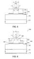
- FIG. 6 is a schematic cross-sectional view of an
SES laser 200 in accordance with a first modified example. TheSES laser 200 in accordance with the first modified example is different from theSES laser 100 of the above-described embodiment in that afirst electrode 214 is provided near the current constrictingsection 105. TheSES laser 200 includes a firstcolumnar section 220 composed of a part of afirst mirror 102, anactive layer 103 and asecond mirror 204. The firstcolumnar section 220 includes a secondcolumnar section 230 provided in its upper portion, and a thirdcolumnar section 240 provided in its lower portion. The secondcolumnar section 230 is formed above the layer where the current constrictingsection 105 is provided. The thirdcolumnar section 240 includes a portion of thefirst mirror 102, theactive layer 103, a portion of thesecond mirror 204, and acurrent constricting section 105. Afirst electrode 214 is formed on a top surface of the thirdcolumnar section 240. Therefore, by improving the conductivity of the topmost layer of the thirdcolumnar section 240, current injection can be more uniformly conducted. Accordingly, a GaAs layer that does not contain Al or an AlGaAs layer that hardly contains Al may preferably be formed in a region of the topmost layer of the thirdcolumnar section 240 on which thefirst electrode 214 is to be formed. - Because the
first electrode 214 is provided near the current constrictingsection 105 as described above, theSES laser 200 can reduce the heat that may be generated by the current flowing through thesecond mirror 204. - It is noted that other portions of the structure and the manufacturing process for the
SES laser 200 in accordance with the first modified example are generally the same as those of the structure and manufacturing process applied to theSES laser 100 in accordance with the embodiment described above, and therefore their description is omitted. - FIG. 7 is a schematic cross-sectional view of an
SES laser 300 in accordance with a second modified example. TheSES laser 300 in accordance with the second modified example is different from theSES laser 100 of the above-described embodiment in that theSES laser 300 is further equipped with atransparent insulation film 301 and aheat radiation film 302. Thetransparent insulation film 301 transmits light emitted from theSES laser 300 and is composed of insulation material. Thetransparent insulation film 301 may be composed of, for example, a silicon nitride (SiN) thin film. The silicon nitride thin film not only has light transmittivity and insulating property, but is also excellent in oxidation resisting property, such that the silicon nitride thin film can prevent oxidation and deterioration of theSES laser 300. Theheat radiation film 302 transmits light at least in a region above an emission surface of theSES laser 300, and is composed of a material having a high thermal conductivity. Theheat radiation film 302 may be composed of, for example, silicon carbide (SiC), diamond (diamond-like-carbon), or sapphire. - The
transparent insulation film 301 and theheat radiation film 302 are composed of materials that transmit light emitted from theSES laser 300, such that theSES laser 300 can emit laser light upwardly. Also, theSES laser 300 has improved heat radiation efficiency because it is equipped with thetransparent insulation film 301 and theheat radiation film 302. As a result of the above, an elevation of the device temperature by the current injection can be suppressed. - Next, an example of a method for manufacturing the
SES laser 300 is described. The steps (1) - (3) for manufacturing theSES laser 100 in accordance with the embodiment described above are conducted, and then atransparent insulation film 301 is formed. Thetransparent insulation film 301 is formed and patterned by known methods. For forming a silicon nitride thin film as thetransparent insulation film 301, a plasma CVD (Chemical Vapor Deposition) method may be used. - Next, a
first electrode 314 and asecond electrode 116 are formed by the method described above, and aheat radiation film 302 is formed. As theheat radiation film 302, silicon carbide, diamond, sapphire or the like can be used, as described above. For example, a sputter method may be used as the film forming method to form a silicon carbide or sapphire film. For example, a CVD method, a sputter method or a thermoelectron impact method may be used as the film forming method to form a diamond film. Then, patterning may be conducted by etching or the like to thereby expose a lead-out section of thefirst electrode 314. Alternatively, a lead-out section of thefirst electrode 314 may be exposed by a lift-off method in which a resist layer is left in advance on an upper surface of the lead-out section, and the resist layer is removed after forming the film. - By the process described above, the
SES laser 300 is manufactured. It is noted that other portions of the structure and manufacturing process for theSES laser 300 in accordance with the second modified example are generally the same as those of the structure and manufacturing process for theSES laser 100 in accordance with the embodiment described above, and therefore their description is omitted. - FIG. 8 is a schematic cross-sectional view of an
SES laser 400 in accordance with a third modified example. TheSES laser 400 in accordance with the third modified example is different from theSES laser 100 of the above-described embodiment in that theSES laser 400 is further equipped with adielectric layer 405 above asecond mirror 404. Thedielectric layer 405 may be composed of alternately laminated layers having different refractive indexes, and can function as a mirror like thesecond mirror 404. Thedielectric layer 405 has a plane configuration that is in, for example, a circular shape having a smaller diameter than that of thesecond mirror 404, but may not be limited to this particular embodiment. Furthermore,concave sections 411 may be formed in the top surface of thesecond mirror 404. Theconcave sections 411 may be formed only in thedielectric layer 405, or theconcave sections 411 may be formed in a manner to penetrate thedielectric layer 405 to thesecond mirror 404. Also, a portion of thedielectric layer 405 may extend into theconcave section 411. As a result, light confinement occurs by the difference between the refractive index of thesecond mirror 404 and the refractive index of thedielectric layer 405 embedded in theconcave sections 411, and the number of oscillation modes is determined by a diameter B inside of theconcave sections 411. - Furthermore, by forming the
dielectric layer 405 that can function as a mirror above thesecond mirror 404, the film thickness of thesecond mirror 404 can be made smaller. As a result, theconcave sections 411 can be formed near theactive layer 103, such that the oscillation mode can be more effectively controlled. - Also, a
first electrode 414 is formed on the top surface of thesecond mirror 404. Thefirst electrode 414 may be formed around thedielectric layer 405. In theSES laser 400 in accordance with the third modified example, the film thickness of thesecond mirror 404 can be made smaller, as described above, and the distance in which current flows through thesecond mirror 404 can be made shorter. As a result, the resistance can be lowered, and heat generation can be reduced. - The
dielectric layer 405 may be formed with Ta2O3, TiO2, Ti2O, Ti, SiO2, SiN or the like, and may be composed of a film of alternately laminated SiO2 and SiN layers. Thedielectric layer 405 can be formed with Si and SiO2. Thedielectric layer 405 may be formed by, for example, plasma CVD, sputtering or the like. - When the mirror is provided using dielectric layers in a manner described above, the refractive index ratio among the layers can be made greater, and the number of pairs can be reduced, compared to the case where the mirror is formed without using dielectric layers. By this, the consumption of material resources can be reduced.
- It is noted that other portions of the structure and manufacturing process for the
SES laser 400 in accordance with the third modified example are generally the same as those of the structure and manufacturing process applied to theSES laser 100 in accordance with the embodiment described above, and therefore their description is omitted. - FIG. 9 is a schematic cross-sectional view of an
SES laser 500 in accordance with a fourth modified example. TheSES laser 500 in accordance with the fourth modified example is different from theSES laser 100 of the above-described embodiment in that theSES laser 500 is further equipped with aconductive film 501, a firstheat radiation film 502, a secondheat radiation film 503 and aninsulation film 506, and does not have afirst electrode 114. TheSES laser 500 in accordance with the fourth modified example has a laserlight emission surface 507 in its lower side, and is therefore different from theSES laser 100 of the above-described embodiment that has an emission surface in its upper side. - The
SES laser 500 in accordance with the fourth modified example further includes adielectric layer 505 formed on the top surface of thesecond mirror 504, like theSES laser 400 in accordance with the third modified example. - The
conductive film 501 is composed of a conductive material, such as, for example, gold-tin (AuSn) and the like, and can function as an electrode for driving theSES laser 500. Theconductive film 501 is formed in a manner to cover thedielectric layer 505, and is in contact with the top surface of thesecond mirror 504. - The first
heat radiation film 502 is formed above theconductive film 501. The firstheat radiation film 502 is composed of a material having a high thermal conductivity. The firstheat radiation film 502 may be composed of, for example, silicon carbide (SiC), diamond (diamond-like-carbon), sapphire or the like. The secondheat radiation film 503 is formed above the firstheat radiation film 502. The secondheat radiation film 503 is composed of a material having a high thermal conductivity. When the secondheat radiation film 503 is composed of a conductive material such as copper, the secondheat radiation film 503 can function as a wiring when it is electrically connected to theconductive film 501. Theinsulation film 506 is formed in a manner to cover the circumference of thesecond mirror 504, the current constrictingsection 105 and theactive layer 103, and the top surface of thefirst mirror 102. - The
semiconductor substrate 101 may be composed of a transparent substrate that transmits light emitted from theSES laser 500. On the other hand, when a transparent substrate is not used, an etching stopper layer may be provided on thesubstrate 101 before thefirst mirror 102a is laminated, and an emission aperture may be provided by etching conducted from the back surface side. Asecond electrode 516 is formed on the back surface of thesemiconductor substrate 101, and has an emission surface 305 in a region surrounded by thesecond electrode 516. By this, theSES laser 500 can emit laser light downwardly. - Next, an example of a method for manufacturing the
SES laser 500 is described. First, the steps (1) - (3) for manufacturing theSES laser 100 in accordance with the embodiment described above are conducted, and then adielectric layer 505 is formed by the method described above. Next, asecond electrode 516 is formed, and then aninsulation film 506 is formed. The material of theinsulation film 506 is not particularly limited, but can be composed of, for example, a silicon nitride thin film. The silicon nitride thin film may be formed by the method described above. - Next, after forming a first
heat radiation film 502 on a secondheat radiation film 503, aconductive film 501 such as a solder film is coated on the firstheat radiation film 502. Then, thefirst mirror 102, theactive layer 103 and thesecond mirror 104 are embedded in theconductive film 501, and then theconductive film 501 is hardened. - By the process described above, the
SES laser 500 is manufactured. In this manner, theSES laser 500 is equipped with theconductive film 501 that can function as an electrode and heat sink, which can contact thesecond mirror 104 in a wider area, whereby its heat radiation efficiency can be increased. By this, an elevation in the device temperature by current injection can be suppressed. Also, theSES laser 500 is equipped with the firstheat radiation film 502 and the secondheat radiation film 503 having high thermal conductivity, which can further increase the heat radiation efficiency. - It is noted that other portions of the structure and manufacturing process for the
SES laser 500 in accordance with the fourth modified example are generally the same as those of the structure and manufacturing process for theSES laser 100 in accordance with the embodiment described above, and therefore their description is omitted. - The invention is not limited to the embodiments described above. For example, a
transparent insulation film 301 and aheat radiation film 302 in accordance with the second modified example may be provided above theSES laser 400 in accordance with the third modified example. The invention may include compositions that are substantially the same as the compositions described in the embodiments (for example, a composition with the same function, method and result, or a composition with the same objects and result). Also, the invention includes compositions in which portions not essential in the compositions described in the embodiments are replaced with others. Also, the invention includes compositions that maintain the same functions and effects or maintain the same objects of those of the compositions described in the embodiments. Furthermore, the invention includes compositions that include publicly known technology added to the compositions described in the embodiments.
Claims (9)
- A surface-emitting type semiconductor laser comprising:a first mirror (102);an active layer (103) formed above the first mirror (102);a second mirror (104, 204, 404, 504) formed above the active layer (103); anda current constricting section (105) formed above or below the active layer (103),wherein the second mirror (104; 204; 404; 504) has a plurality of concave sections (111, 411) arranged within a plane perpendicular to a light emission direction, and a light confining region (110) surrounded by the concave sections (111; 411) is formed inside a region surrounded by the current constricting section (105) as viewed in a plan view.
- The semiconductor laser according to claim 1, comprising:a first columnar section (220) formed from at least the active layer (103), the second mirror (204) and the current constricting section (105),wherein the first columnar section (220) includes a third columnar section (240) having the active layer (103) and the current constricting section (105) and a second columnar section (230) formed above the third columnar section (240), and an electrode formed on a top surface of the third columnar section (240) and around the second columnar section (230).
- The semiconductor laser according to claim 1, comprising a heat radiation film (302; 502, 503) formed above the second mirror (204).
- The semiconductor laser according to claim 3, wherein the heat radiation film (302) has optical transparency.
- The semiconductor laser according to claim 3, wherein the heat radiation film (503) is composed of a electrically conductive material, and further comprising an insulation layer having optical transparency provided between the second mirror (504) and the heat radiation film (502, 503).
- The semiconductor laser according to claim 5, wherein the insulation film is embedded inside the concave sections (411).
- A surface-emitting type semiconductor laser according to claim 1, further comprising:a electrically conductive film (501) formed on an entire surface above the second mirror (504);a first heat radiation film (502) formed above the conductive film (501); anda second heat radiation film (503) formed above the first heat radiation film (502),wherein the conductive film (501) functions as an electrode for driving the surface-emitting type semiconductor laser, and the second heat radiation film (503) is composed of an electrically conductive material and is electrically connected to the conductive film (501).
- The semiconductor laser according to any one of the preceding claims 1, wherein the second mirror (104; 204; 404; 504) includes a dielectric mirror.
- The semiconductor laser according to claim 1, further comprising a dielectric layer (501) formed above the second mirror (504), wherein a lowermost layer of the dielectric mirror is embedded in the concave sections (411).
Applications Claiming Priority (1)
| Application Number | Priority Date | Filing Date | Title |
|---|---|---|---|
| JP2006005322A JP4548345B2 (en) | 2006-01-12 | 2006-01-12 | Surface emitting semiconductor laser |
Publications (2)
| Publication Number | Publication Date |
|---|---|
| EP1811620A2 true EP1811620A2 (en) | 2007-07-25 |
| EP1811620A3 EP1811620A3 (en) | 2007-11-21 |
Family
ID=38120054
Family Applications (1)
| Application Number | Title | Priority Date | Filing Date |
|---|---|---|---|
| EP07000563A Withdrawn EP1811620A3 (en) | 2006-01-12 | 2007-01-12 | Surface emitting type semiconductor laser |
Country Status (4)
| Country | Link |
|---|---|
| US (1) | US7397835B2 (en) |
| EP (1) | EP1811620A3 (en) |
| JP (1) | JP4548345B2 (en) |
| KR (1) | KR20070075337A (en) |
Cited By (4)
| Publication number | Priority date | Publication date | Assignee | Title |
|---|---|---|---|---|
| US20220352693A1 (en) * | 2021-04-30 | 2022-11-03 | Lumentum Operations Llc | Methods for incorporating a control structure within a vertical cavity surface emitting laser device cavity |
| EP3930122A4 (en) * | 2019-02-21 | 2022-11-30 | Stanley Electric Co., Ltd. | VERTICAL RESONATOR TYPE ELECTROLUMINESCENT DEVICE |
| US12218486B2 (en) | 2018-10-18 | 2025-02-04 | Stanley Electric Co., Ltd. | Vertical cavity surface emitting device |
| US12308614B2 (en) | 2018-10-18 | 2025-05-20 | Stanley Electric Co., Ltd. | Vertical cavity surface emitting device |
Families Citing this family (7)
| Publication number | Priority date | Publication date | Assignee | Title |
|---|---|---|---|---|
| US7883914B2 (en) * | 2006-05-29 | 2011-02-08 | Alight Technologies A/S | Method for fabricating a photonic crystal or photonic bandgap vertical-cavity surface-emitting laser |
| JP4766704B2 (en) * | 2007-04-20 | 2011-09-07 | キヤノン株式会社 | Surface emitting laser |
| JP6240429B2 (en) | 2013-08-07 | 2017-11-29 | 国立大学法人東京工業大学 | Surface emitting semiconductor laser and optical transmission device |
| JP5721246B1 (en) | 2014-08-08 | 2015-05-20 | 国立大学法人東京工業大学 | Surface emitting laser with light modulation function |
| JP2016174136A (en) * | 2015-03-16 | 2016-09-29 | 株式会社リコー | Surface emitting laser array, laser device, ignition device, and internal combustion engine |
| KR102384228B1 (en) * | 2015-09-30 | 2022-04-07 | 삼성전자주식회사 | Semiconductor laser resonator and Semiconductor laser device having the same |
| FR3078834B1 (en) * | 2018-03-08 | 2020-03-27 | Commissariat A L'energie Atomique Et Aux Energies Alternatives | LIGHT EMITTING DEVICE COMPRISING AT LEAST ONE VCSEL AND A DIFFUSION LENS |
Family Cites Families (9)
| Publication number | Priority date | Publication date | Assignee | Title |
|---|---|---|---|---|
| JPH0738196A (en) * | 1993-07-22 | 1995-02-07 | Nec Corp | Surface light emitting element |
| US5422901A (en) * | 1993-11-15 | 1995-06-06 | Motorola, Inc. | Semiconductor device with high heat conductivity |
| JP2000196189A (en) * | 1998-12-24 | 2000-07-14 | Toshiba Corp | Surface emitting semiconductor laser |
| DK1371120T3 (en) | 2001-03-09 | 2013-07-22 | Alight Photonics Aps | WAVE TYPE CONTROL USING TRANSVERSAL TAPE STRUCTURE IN VCSELS |
| JP3692060B2 (en) | 2001-09-14 | 2005-09-07 | 株式会社東芝 | Vertical cavity type semiconductor light emitting device |
| US7085301B2 (en) * | 2002-07-12 | 2006-08-01 | The Board Of Trustees Of The University Of Illinois | Photonic crystal single transverse mode defect structure for vertical cavity surface emitting laser |
| JP4641736B2 (en) | 2003-10-28 | 2011-03-02 | ソニー株式会社 | Surface emitting semiconductor laser, method of manufacturing the same, and optical apparatus |
| US7483469B2 (en) * | 2004-11-01 | 2009-01-27 | Seiko Epson Corporation | Surface-emitting type semiconductor laser and its manufacturing method, optical module, and light transmission device |
| JP2007173514A (en) * | 2005-12-22 | 2007-07-05 | Fuji Xerox Co Ltd | Optical information processing equipment using large-diameter surface-emitting semiconductor laser elements. |
-
2006
- 2006-01-12 JP JP2006005322A patent/JP4548345B2/en not_active Expired - Fee Related
- 2006-12-04 US US11/566,402 patent/US7397835B2/en not_active Expired - Fee Related
-
2007
- 2007-01-11 KR KR1020070003178A patent/KR20070075337A/en not_active Withdrawn
- 2007-01-12 EP EP07000563A patent/EP1811620A3/en not_active Withdrawn
Cited By (5)
| Publication number | Priority date | Publication date | Assignee | Title |
|---|---|---|---|---|
| US12218486B2 (en) | 2018-10-18 | 2025-02-04 | Stanley Electric Co., Ltd. | Vertical cavity surface emitting device |
| US12308614B2 (en) | 2018-10-18 | 2025-05-20 | Stanley Electric Co., Ltd. | Vertical cavity surface emitting device |
| EP3930122A4 (en) * | 2019-02-21 | 2022-11-30 | Stanley Electric Co., Ltd. | VERTICAL RESONATOR TYPE ELECTROLUMINESCENT DEVICE |
| US20220352693A1 (en) * | 2021-04-30 | 2022-11-03 | Lumentum Operations Llc | Methods for incorporating a control structure within a vertical cavity surface emitting laser device cavity |
| US12362541B2 (en) * | 2021-04-30 | 2025-07-15 | Lumentum Operations Llc | Methods for incorporating a control structure within a vertical cavity surface emitting laser device cavity |
Also Published As
| Publication number | Publication date |
|---|---|
| JP2007189033A (en) | 2007-07-26 |
| US7397835B2 (en) | 2008-07-08 |
| JP4548345B2 (en) | 2010-09-22 |
| US20070258499A1 (en) | 2007-11-08 |
| KR20070075337A (en) | 2007-07-18 |
| EP1811620A3 (en) | 2007-11-21 |
Similar Documents
| Publication | Publication Date | Title |
|---|---|---|
| EP1811620A2 (en) | Surface emitting type semiconductor laser | |
| EP1808944B1 (en) | Surface-emitting type semiconductor laser | |
| JP5707742B2 (en) | Vertical cavity surface emitting laser | |
| TWI426674B (en) | Photoelectric component and method of manufacturing optoelectronic component | |
| US6201825B1 (en) | Surface emitting semiconductor laser device and process for producing the same | |
| JP2005340567A (en) | Surface luminescence type semiconductor laser element and its manufacturing method | |
| EP1798827A2 (en) | Surface-emitting type semiconductor laser and method for manufacturing the same | |
| CN120222148B (en) | Vertical cavity surface emitting laser and manufacturing method thereof | |
| JP4224981B2 (en) | Surface emitting semiconductor laser device and method for manufacturing the same | |
| US7929588B2 (en) | Semiconductor devices and methods for generating light | |
| US8183649B2 (en) | Buried aperture nitride light-emitting device | |
| US7440481B2 (en) | Surface-emitting type semiconductor laser and method for manufacturing the same | |
| US20070133641A1 (en) | Surface-emitting type semiconductor laser and method for manufacturing the same | |
| JP2003309325A (en) | Surface emitting semiconductor laser device and method of manufacturing the same | |
| US20260081402A1 (en) | Radiation emitter and method of fabricating radiation emitters | |
| US6621844B1 (en) | Buried oxide photonic device with large contact and precise aperture | |
| EP4528946A1 (en) | Radiation emitter and method of fabricating radiation emitters | |
| US11569635B2 (en) | Radiation-emitting semiconductor component | |
| KR100244237B1 (en) | Embedded semiconductor laser diode | |
| JP2018160649A (en) | Vertical resonance type plane emission semiconductor laser | |
| JP2007311617A (en) | Semiconductor device and manufacturing method thereof | |
| JP5041421B2 (en) | Surface emitting laser device manufacturing method and surface emitting laser device | |
| JP2008177341A (en) | Surface emitting semiconductor laser and manufacturing method thereof | |
| CN1479960A (en) | Optoelectronic device with highly conductive carrier tunneling current aperture |
Legal Events
| Date | Code | Title | Description |
|---|---|---|---|
| PUAI | Public reference made under article 153(3) epc to a published international application that has entered the european phase |
Free format text: ORIGINAL CODE: 0009012 |
|
| AK | Designated contracting states |
Kind code of ref document: A2 Designated state(s): AT BE BG CH CY CZ DE DK EE ES FI FR GB GR HU IE IS IT LI LT LU LV MC NL PL PT RO SE SI SK TR |
|
| AX | Request for extension of the european patent |
Extension state: AL BA HR MK YU |
|
| PUAL | Search report despatched |
Free format text: ORIGINAL CODE: 0009013 |
|
| AK | Designated contracting states |
Kind code of ref document: A3 Designated state(s): AT BE BG CH CY CZ DE DK EE ES FI FR GB GR HU IE IS IT LI LT LU LV MC NL PL PT RO SE SI SK TR |
|
| AX | Request for extension of the european patent |
Extension state: AL BA HR MK YU |
|
| 17P | Request for examination filed |
Effective date: 20080514 |
|
| AKX | Designation fees paid |
Designated state(s): DE DK GB |
|
| 17Q | First examination report despatched |
Effective date: 20090602 |
|
| STAA | Information on the status of an ep patent application or granted ep patent |
Free format text: STATUS: THE APPLICATION IS DEEMED TO BE WITHDRAWN |
|
| 18D | Application deemed to be withdrawn |
Effective date: 20091013 |