EP1811569A2 - Organic light emitting display - Google Patents
Organic light emitting display Download PDFInfo
- Publication number
- EP1811569A2 EP1811569A2 EP07001187A EP07001187A EP1811569A2 EP 1811569 A2 EP1811569 A2 EP 1811569A2 EP 07001187 A EP07001187 A EP 07001187A EP 07001187 A EP07001187 A EP 07001187A EP 1811569 A2 EP1811569 A2 EP 1811569A2
- Authority
- EP
- European Patent Office
- Prior art keywords
- electrode
- light emitting
- organic light
- emitting diode
- driving unit
- Prior art date
- Legal status (The legal status is an assumption and is not a legal conclusion. Google has not performed a legal analysis and makes no representation as to the accuracy of the status listed.)
- Granted
Links
Images

Classifications
-
- H—ELECTRICITY
- H10—SEMICONDUCTOR DEVICES; ELECTRIC SOLID-STATE DEVICES NOT OTHERWISE PROVIDED FOR
- H10K—ORGANIC ELECTRIC SOLID-STATE DEVICES
- H10K59/00—Integrated devices, or assemblies of multiple devices, comprising at least one organic light-emitting element covered by group H10K50/00
- H10K59/10—OLED displays
- H10K59/12—Active-matrix OLED [AMOLED] displays
- H10K59/128—Active-matrix OLED [AMOLED] displays comprising two independent displays, e.g. for emitting information from two major sides of the display
-
- H—ELECTRICITY
- H10—SEMICONDUCTOR DEVICES; ELECTRIC SOLID-STATE DEVICES NOT OTHERWISE PROVIDED FOR
- H10K—ORGANIC ELECTRIC SOLID-STATE DEVICES
- H10K50/00—Organic light-emitting devices
- H10K50/80—Constructional details
- H10K50/805—Electrodes
- H10K50/82—Cathodes
- H10K50/826—Multilayers, e.g. opaque multilayers
-
- H—ELECTRICITY
- H10—SEMICONDUCTOR DEVICES; ELECTRIC SOLID-STATE DEVICES NOT OTHERWISE PROVIDED FOR
- H10K—ORGANIC ELECTRIC SOLID-STATE DEVICES
- H10K59/00—Integrated devices, or assemblies of multiple devices, comprising at least one organic light-emitting element covered by group H10K50/00
- H10K59/10—OLED displays
- H10K59/12—Active-matrix OLED [AMOLED] displays
- H10K59/123—Connection of the pixel electrodes to the thin film transistors [TFT]
-
- H—ELECTRICITY
- H10—SEMICONDUCTOR DEVICES; ELECTRIC SOLID-STATE DEVICES NOT OTHERWISE PROVIDED FOR
- H10K—ORGANIC ELECTRIC SOLID-STATE DEVICES
- H10K59/00—Integrated devices, or assemblies of multiple devices, comprising at least one organic light-emitting element covered by group H10K50/00
- H10K59/80—Constructional details
- H10K59/805—Electrodes
- H10K59/8052—Cathodes
- H10K59/80523—Multilayers, e.g. opaque multilayers
Definitions
- This document relates to an organic light emitting display (OLED).
- light emitting display has an advantage in that it has high response speed and low power consumption.
- the light emitting display can also be manufactured thin in size and light in weight because of not requiring backlight unit.
- organic light emitting display has an organic light emitting layer between an anode and a cathode. Holes from the anode and electrons from the cathode are combined within the organic light emitting layer to create hole-electron pairs, i.e., excitons. The OLED emits lights by energy generated while the excitons return to ground state.
- dual emission type OLED was fabricated such that two panels were separately fabricated and then attached. In this case, the fabrication cost of the device increased and the device became thick because the two separate panels were attached.
- dual emission type OLED comprised sub-pixels each having a top emission region and a bottom emission region. But, the device cannot obtain a sufficient emitting area because each single pixel is divided into the two parts, so its luminance is reduced.
- An aspect of this document is to provide an organic light emitting display (OLED) which is fabricated at a low cost, thinner and has an improved luminance.
- OLED organic light emitting display
- the OLED comprises a substrate, first and second driving units positioned on the substrate, a first light emitting diode (LED) connected with the first driving unit and comprising a first organic light emitting layer and a second emitting diode electrically connected with the second driving unit and comprising a second organic light emitting layer.
- LED light emitting diode
- FIG. 1 is a sectional view showing an organic light emitting display (OLED) according to a first embodiment of this document.
- OLED organic light emitting display
- FIG. 2 is a sectional view showing an OLED according to a second embodiment of this document.
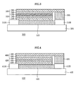
- FIG. 3 is a sectional view showing an OLED according to a third embodiment of this document.
- FIG. 4 is a sectional view showing an OLED according to a fourth embodiment of this document.
- an organic light emitting display (OLED) 100 comprises a first unit and a second driving unit 110A and 110B positioned on a substrate 105.
- the first and second driving units 110A and 110B comprise at least one driving transistor, respectively.
- the driving transistor may comprise a semiconductor layer, a gate electrode positioned corresponding to the semiconductor layer, a gate insulation layer positioned between the semiconductor layer and the gate electrode, and source and drain electrodes electrically connected with the semiconductor layer.
- the first and second driving units 110A and 110B may further comprise a switching transistor and a capacitor, respectively.
- An insulation layer 115 is positioned on the first and second driving units 110A and 110B.
- the insulation layer 115 can be an insulation layer for planarization and comprise a transparent dielectric material.
- the insulation layer 115 can be formed to expose the source and drain electrodes of the driving units 110A and 110B.
- the insulation layer 115 is formed to be lower than the driving units 110A and 110B, but without being limited thereto, the insulation layer 115 can be formed to be higher than the driving units 110A and 110B so long as it can expose the source or drain electrode of the driving units 110A and 110B via a via hole.
- a first emitting diode 120 electrically connected with the first driving unit 110A is positioned on the first driving unit 110A and the insulation layer 115.
- a second emitting diode 160 electrically connected with the second driving unit 110B is positioned on the first emitting diode 120.
- the first emitting diode 120 comprises a first anode 130, a first organic light emitting layer 140 and a first cathode 150
- the second emitting diode 160 comprises a second anode 170, a second organic light emitting layer 180 and a second cathode 190. Accordingly, the first cathode 150 and the second anode 170 electrically contact with each other.
- the first anode 130 of the first emitting diode 120 is electrically connected with the first driving unit 110A
- the second cathode 190 of the second emitting diode 160 is electrically connected with the second driving unit 110B.
- a connection layer 195 can be positioned on the second driving unit 110B.
- the second cathode 190 can be electrically connected with the second driving unit 110B via the connection layer 195.
- a metal wiring for supplying power can be connected with the first cathode 150 and the second anode 170.
- the first and second anodes 130 and 170 may comprise a material with a high work function, for example, indium tin oxide (ITO), and the first and second cathodes 150 and 190 may comprise one or more of metals such as Al, Ca, Mg, and LIF/Al which have a low work function and high reflexibility.
- the second cathode 190 can be a transflective electrode comprising a transparent conductive layer and a metallic layer or a transflective electrode made of a thin metal.
- first cathode 150 comprising metal is positioned under the second anode 170, light generated from the second emitting diode 160 can be reflected by the first cathode 150 and then emitted to an upper side of the second emitting diode 160. Light generated from the first emitting diode 120 can be reflected by the first cathode 150 and then emitted to a lower side of the first emitting diode 120.
- the dual emission type OLED can be implemented without reducing an aperture ratio.
- first emitting diode 120 and the second emitting diode 160 are electrically connected with the first and second driving units 110A and 110B, respectively, they can be separately driven, so power consumption can be reduced and the screens can be effectively changed.
- an OLED 200 includes first and second driving units 210A and 210B positioned on a substrate 205.
- the first and second driving units 210A and 210B comprise at least one driving transistor, respectively.
- a first insulation layer 215 is positioned on the first and second driving units 210A and 210B.
- the first insulation layer 215 can be formed to expose source or drain electrode of the first and second driving units 210A and 210B.
- a first emitting diode 220 electrically connected with the first driving unit 210A is positioned on the first driving unit 210A and the first insulation layer 215.
- a second emitting diode 260 electrically connected with the second driving unit 210B is positioned on the first emitting diode 220, and a second insulation layer 255 is positioned between the first and second emitting diodes 220 and 260.
- the first emitting diode 220 includes a first anode 230, a first organic light emitting layer 240 and a first cathode 250
- the second emitting diode 260 includes a second anode 270, a second organic light emitting layer 280 and a second cathode 290.
- the first anode 230 of the first emitting diode 220 is electrically connected with the first driving unit 210A
- the second cathode 290 is electrically connected with the second driving unit 210B.
- a connection layer 295 can be positioned on the second driving unit. Accordingly, the second cathode 290 can be electrically connected with the second driving unit 210B via the connection layer 295.
- a metal wiring for supplying power can be connected with the first cathode 250 and the second anode 270.
- the first and second anodes 230 and 270 may comprise a material with a high work function, for example, ITO, and the first and second cathodes 250 and 290 may comprise one or more of metals such as Al, Ca, Mg, and LIF/Al which have a low work function and high reflexibility.
- the second cathode 290 can be a thin transflective electrode.
- first cathode 250 comprising metal is positioned under the second anode 270, light generated from the second emitting diode 260 can be reflected by the first cathode 250 and then emitted to an upper side of the second emitting diode 260. Light generated from the first emitting diode 220 can be reflected by the first cathode 250 and then emitted to a lower side of the first emitting diode 220.
- the first and second emitting diodes 220 and 260 are electrically connected with the first and second driving units 210A and 210B, respectively, the first and second emitting diodes 220 and 260 can be driven separately.
- Electrodes that comprise each different material cannot contact with each other, because the second insulation layer 255 is positioned between the first and second emitting diodes 220 and 260, so a driving voltage can be reduced.
- an OLED 300 includes first and second driving units 310A and 310B positioned on a substrate 305.
- the first and second driving units 310A and 310B comprise at least one driving transistor, respectively.
- An insulation layer 315 is positioned on the first and second driving units 310A and 310B.
- the insulation layer 315 can be formed to expose source or drain electrode of the first and second driving units 310A and 310B.
- a first emitting diode 320 electrically connected with the first driving unit 310A is positioned on the first driving unit 310A and the insulation layer 315.
- a second emitting diode 360 electrically connected with the second driving unit 310B is positioned on the first emitting diode 320.
- a first electrode 330 is positioned under a first organic light emitting layer 340
- a second electrode 390 is positioned on a second organic light emitting layer 380
- a third electrode 350 is positioned between the first and second organic light emitting layers 340 and 380.
- the first and second electrodes 330 and 390 are anodes of the first and second emitting diodes 320 and 360, respectively, and the third electrode 350 is a common cathode of the first and second emitting diodes 320 and 360.
- the first electrode 330 is electrically connected with the first driving unit 310A
- the second electrode 390 is electrically connected with the second driving unit 310B.
- an connection layer 395 can be positioned on the second driving unit 310B to resolve the step.
- the second electrode 390 can be electrically connected with the second driving unit 310B via the connection layer 395.
- a metal wiring for supplying power can be connected with the third electrode 350.
- the first and second electrodes 330 and 390 may comprise a material with a high work function, for example, ITO, and the third electrode 350 may comprise one or more of metals such as Al, Ca, Mg, and LIF/Al which have a low work function and high reflexibility.
- the OLED 300 according to the third embodiment of the present invention has such advantage in that it has a large emitting area and a separate driving can be possibly performed.
- the OLED 300 uses the third electrode 350 as the common cathode of the first and second emitting diodes 320 and 360, a processing time and cost for its fabrication can be reduced and the OLED can be implemented to be thinner.
- a first electrode 400 is used as an anode of a first emitting diode 420 and a third electrode 490 is used as a cathode of the second emitting diode 490.
- a third electrode 450 is used as a cathode of the first emitting diode 420 and as an anode of a second emitting diode 460.
- the third electrode 450 is used as the common electrode of the first and second emitting diodes 420 and 460, it plays a different role in each emitting diode. Thus, in this case, the third electrode 450 cannot have a proper work function in performing the two roles.
- the third electrode 450 can be made of a metal having a low work function, and surface treatment is performed on one surface of the third electrode to have a high work function by using at least one of mechanical, chemical, plasma, laser surface processing methods in order to increase the work function.
- the treated surface of the third electrode is opposite to the second emitting layer in third electrode
- the second electrode 450 can perform the role of the cathode of the first emitting diode 420 by comprising a metal having a low work function and also perform the role of the anode of the second emitting diode 460 by comprising one surface having a high work function.
- the first and second driving units are positioned on the same planar surface, but without being limited thereto, the second driving unit can be formed to be positioned on the first driving unit.
- the first driving unit is formed, an insulation layer can be formed on the first driving unit, and then, the second driving unit can be formed on the insulation layer.
Landscapes
- Engineering & Computer Science (AREA)
- Microelectronics & Electronic Packaging (AREA)
- Electroluminescent Light Sources (AREA)
- Control Of Indicators Other Than Cathode Ray Tubes (AREA)
Abstract
Description
- This document relates to an organic light emitting display (OLED).
- Among flat panel display devices, light emitting display has an advantage in that it has high response speed and low power consumption. The light emitting display can also be manufactured thin in size and light in weight because of not requiring backlight unit.
- In particularly, organic light emitting display (OLED) has an organic light emitting layer between an anode and a cathode. Holes from the anode and electrons from the cathode are combined within the organic light emitting layer to create hole-electron pairs, i.e., excitons. The OLED emits lights by energy generated while the excitons return to ground state.
- Recently, dual emission type OLED is increasingly employed for mobile communication devices such as mobile phones.
- In one related art, dual emission type OLED was fabricated such that two panels were separately fabricated and then attached. In this case, the fabrication cost of the device increased and the device became thick because the two separate panels were attached.
- In another related art, dual emission type OLED comprised sub-pixels each having a top emission region and a bottom emission region. But, the device cannot obtain a sufficient emitting area because each single pixel is divided into the two parts, so its luminance is reduced.
- An aspect of this document is to provide an organic light emitting display (OLED) which is fabricated at a low cost, thinner and has an improved luminance.
- In an aspect, the OLED comprises a substrate, first and second driving units positioned on the substrate, a first light emitting diode (LED) connected with the first driving unit and comprising a first organic light emitting layer and a second emitting diode electrically connected with the second driving unit and comprising a second organic light emitting layer.
- The implementation of this document will be described in detail Referring to the following drawings in which like numerals refer to like elements.
- FIG. 1 is a sectional view showing an organic light emitting display (OLED) according to a first embodiment of this document.
- FIG. 2 is a sectional view showing an OLED according to a second embodiment of this document.
- FIG. 3 is a sectional view showing an OLED according to a third embodiment of this document.
- FIG. 4 is a sectional view showing an OLED according to a fourth embodiment of this document.
- Hereinafter, an implementation of this document will be described in detail referring to the attached drawings.
- [First embodiment]
- Referring to FIG. 1, an organic light emitting display (OLED) 100 according to a first embodiment of the present invention comprises a first unit and a
second driving unit substrate 105. The first andsecond driving units second driving units - An
insulation layer 115 is positioned on the first andsecond driving units insulation layer 115 can be an insulation layer for planarization and comprise a transparent dielectric material. Theinsulation layer 115 can be formed to expose the source and drain electrodes of thedriving units insulation layer 115 is formed to be lower than thedriving units insulation layer 115 can be formed to be higher than thedriving units driving units - A
first emitting diode 120 electrically connected with thefirst driving unit 110A is positioned on thefirst driving unit 110A and theinsulation layer 115. And asecond emitting diode 160 electrically connected with thesecond driving unit 110B is positioned on thefirst emitting diode 120. - Here, the
first emitting diode 120 comprises afirst anode 130, a first organiclight emitting layer 140 and afirst cathode 150, and thesecond emitting diode 160 comprises a second anode 170, a second organic light emitting layer 180 and asecond cathode 190. Accordingly, thefirst cathode 150 and the second anode 170 electrically contact with each other. - The
first anode 130 of thefirst emitting diode 120 is electrically connected with thefirst driving unit 110A, and thesecond cathode 190 of thesecond emitting diode 160 is electrically connected with thesecond driving unit 110B. In this case, because of height difference between thesecond emitting diode 160 and thesecond driving unit 110B, aconnection layer 195 can be positioned on thesecond driving unit 110B. Thus, thesecond cathode 190 can be electrically connected with thesecond driving unit 110B via theconnection layer 195. - Although not shown, a metal wiring for supplying power can be connected with the
first cathode 150 and the second anode 170. - The first and
second anodes 130 and 170 may comprise a material with a high work function, for example, indium tin oxide (ITO), and the first andsecond cathodes second cathode 190 can be a transflective electrode comprising a transparent conductive layer and a metallic layer or a transflective electrode made of a thin metal. - Because the
first cathode 150 comprising metal is positioned under the second anode 170, light generated from thesecond emitting diode 160 can be reflected by thefirst cathode 150 and then emitted to an upper side of thesecond emitting diode 160. Light generated from thefirst emitting diode 120 can be reflected by thefirst cathode 150 and then emitted to a lower side of thefirst emitting diode 120. - As described above, in the first embodiment of the present invention, with the bottom-emission type
first emitting diode 120 and the top-emission typesecond emitting diode 160 formed in the stacked structure, the dual emission type OLED can be implemented without reducing an aperture ratio. - In addition, because the
first emitting diode 120 and thesecond emitting diode 160 are electrically connected with the first andsecond driving units - [Second embodiment]
- Referring to FIG. 2, an OLED 200 according to a second embodiment of the present invention includes first and
second driving units substrate 205. The first andsecond driving units - A
first insulation layer 215 is positioned on the first andsecond driving units first insulation layer 215 can be formed to expose source or drain electrode of the first andsecond driving units - A first emitting diode 220 electrically connected with the
first driving unit 210A is positioned on thefirst driving unit 210A and thefirst insulation layer 215. Asecond emitting diode 260 electrically connected with thesecond driving unit 210B is positioned on the first emitting diode 220, and a second insulation layer 255 is positioned between the first andsecond emitting diodes 220 and 260. - Here, the first emitting diode 220 includes a
first anode 230, a first organic light emitting layer 240 and a first cathode 250, and thesecond emitting diode 260 includes asecond anode 270, a second organiclight emitting layer 280 and asecond cathode 290. - The
first anode 230 of the first emitting diode 220 is electrically connected with thefirst driving unit 210A, and thesecond cathode 290 is electrically connected with thesecond driving unit 210B. In this case, because of height difference between thesecond emitting diode 260 and thesecond driving unit 210B, aconnection layer 295 can be positioned on the second driving unit. Accordingly, thesecond cathode 290 can be electrically connected with thesecond driving unit 210B via theconnection layer 295. - Although not shown, a metal wiring for supplying power can be connected with the first cathode 250 and the
second anode 270. - The first and
second anodes second cathodes 250 and 290 may comprise one or more of metals such as Al, Ca, Mg, and LIF/Al which have a low work function and high reflexibility. In particular, thesecond cathode 290 can be a thin transflective electrode. - Because the first cathode 250 comprising metal is positioned under the
second anode 270, light generated from thesecond emitting diode 260 can be reflected by the first cathode 250 and then emitted to an upper side of thesecond emitting diode 260. Light generated from the first emitting diode 220 can be reflected by the first cathode 250 and then emitted to a lower side of the first emitting diode 220. - As described above, in the second embodiment of the present invention, with the bottom-emission type first emitting diode 220 and the top-emission type
second emitting diode 260 formed in the stacked structure, an aperture ratio of the OLED is not reduced. In addition, because the first andsecond emitting diodes 220 and 260 are electrically connected with the first andsecond driving units second emitting diodes 220 and 260 can be driven separately. - Also electrodes that comprise each different material cannot contact with each other, because the second insulation layer 255 is positioned between the first and second emitting
diodes 220 and 260, so a driving voltage can be reduced. - [Third embodiment]
- Referring to FIG. 3, an
OLED 300 according to a third embodiment of the present invention includes first andsecond driving units substrate 305. The first andsecond driving units - An
insulation layer 315 is positioned on the first andsecond driving units insulation layer 315 can be formed to expose source or drain electrode of the first andsecond driving units - A first emitting
diode 320 electrically connected with thefirst driving unit 310A is positioned on thefirst driving unit 310A and theinsulation layer 315. A second emittingdiode 360 electrically connected with thesecond driving unit 310B is positioned on the first emittingdiode 320. - Here, a
first electrode 330 is positioned under a first organiclight emitting layer 340, asecond electrode 390 is positioned on a second organiclight emitting layer 380, and athird electrode 350 is positioned between the first and second organiclight emitting layers - Namely, the first and
second electrodes diodes third electrode 350 is a common cathode of the first and second emittingdiodes - The
first electrode 330 is electrically connected with thefirst driving unit 310A, and thesecond electrode 390 is electrically connected with thesecond driving unit 310B. In this case, because of height difference between the secondemitting diode 360 and thesecond driving unit 310B, anconnection layer 395 can be positioned on thesecond driving unit 310B to resolve the step. Accordingly, thesecond electrode 390 can be electrically connected with thesecond driving unit 310B via theconnection layer 395. Although not shown, a metal wiring for supplying power can be connected with thethird electrode 350. - The first and
second electrodes third electrode 350 may comprise one or more of metals such as Al, Ca, Mg, and LIF/Al which have a low work function and high reflexibility. - Accordingly, light generated from the first and second organic
light emitting layers third electrode 350, the common cathode, and emitted toward the first andsecond electrodes - As described above, the
OLED 300 according to the third embodiment of the present invention has such advantage in that it has a large emitting area and a separate driving can be possibly performed. - In addition, because the
OLED 300 uses thethird electrode 350 as the common cathode of the first and second emittingdiodes - [Fourth embodiment]
- Referring to FIG. 4, in the OLED according to the fourth embodiment of the present invention, a
first electrode 400 is used as an anode of a firstemitting diode 420 and athird electrode 490 is used as a cathode of the secondemitting diode 490. Athird electrode 450 is used as a cathode of the first emittingdiode 420 and as an anode of a secondemitting diode 460. - Although the
third electrode 450 is used as the common electrode of the first and second emittingdiodes third electrode 450 cannot have a proper work function in performing the two roles. - Thus, the
third electrode 450 can be made of a metal having a low work function, and surface treatment is performed on one surface of the third electrode to have a high work function by using at least one of mechanical, chemical, plasma, laser surface processing methods in order to increase the work function. The treated surface of the third electrode is opposite to the second emitting layer in third electrode - In other words, the
second electrode 450 can perform the role of the cathode of the first emittingdiode 420 by comprising a metal having a low work function and also perform the role of the anode of the secondemitting diode 460 by comprising one surface having a high work function. - In the above-described embodiments of the present invention, the first and second driving units are positioned on the same planar surface, but without being limited thereto, the second driving unit can be formed to be positioned on the first driving unit. In this case, after the first driving unit is formed, an insulation layer can be formed on the first driving unit, and then, the second driving unit can be formed on the insulation layer.
- Although the present invention has been described with reference to certain exemplary embodiments, it will be understood by those skilled in the art that a variety of modifications and variations may be made to the present invention without departing from the spirit or scope of the present invention defined in the appended claims, and their equivalents.
Claims (11)
- An organic light emitting display comprising:a substrate;a first and a second driving units positioned on the substrate; anda first light emitting diode (LED) connected with the first driving unit and comprising a first organic light emitting layer and a second emitting diode electrically connected with the second driving unit and comprising a second organic light emitting layer,wherein the second emitting diode is positioned on the first emitting diode.
- The display of claim 1, wherein the first emitting diode is a bottom-emission type and the second emitting diode is a top-emission type.
- The display of claim 1, wherein the first emitting diode comprises a first electrode positioned at a lower portion of the first organic light emitting layer and electrically connected with the first driving unit and a second electrode positioned at an upper portion of the first organic light emitting layer, and the second emitting diode comprises a third electrode positioned at a lower portion of the second organic light emitting layer and a fourth electrode positioned at an upper portion of the second organic light emitting layer and electrically connected with the second driving unit.
- The display of claim 3, wherein the fourth electrode is a transflective electrode.
- The display of claim 4, wherein the first and third electrodes are anodes, the second and fourth electrodes are cathodes, and the second and third electrodes electrically contact with each other.
- The display of claim 4, wherein the first and third electrodes are anodes, the second and fourth electrodes are cathodes, and an insulation layer is positioned between the first and second emitting diodes.
- The display of claim 1, wherein the first electrode electrically connected with the first driving unit is positioned at the first organic light emitting layer, the second electrode electrically connected with the second driving unit is positioned at the upper portion of the second organic light emitting layer, and the third electrode is positioned between the first and second organic light emitting layers.
- The display of claim 7, wherein the first and second electrodes are anodes, and the third electrode is a cathode.
- The display of claim 7, wherein the first electrode is an anode, the second electrode is a cathode, and the third electrode comprises a matal having a low work function, a surface opposing the second emitting layer in the third electrode is surface-treated.
- The display of claim 9, wherein the surface treatment is one selected from the group consisting of a mechanical treatment, a chemical treatment, a plasma treatment, and a laser treatment.
- The display of claim 1, wherein the second driving unit is positioned on the first driving unit.
Applications Claiming Priority (2)
| Application Number | Priority Date | Filing Date | Title |
|---|---|---|---|
| KR1020060006010A KR101294845B1 (en) | 2006-01-19 | 2006-01-19 | Light Emitting Diode and Method for Manufacturing the same |
| KR1020060006537A KR100741781B1 (en) | 2006-01-20 | 2006-01-20 | Duplex display |
Publications (3)
| Publication Number | Publication Date |
|---|---|
| EP1811569A2 true EP1811569A2 (en) | 2007-07-25 |
| EP1811569A3 EP1811569A3 (en) | 2010-07-14 |
| EP1811569B1 EP1811569B1 (en) | 2018-07-25 |
Family
ID=38015426
Family Applications (1)
| Application Number | Title | Priority Date | Filing Date |
|---|---|---|---|
| EP07001187.9A Active EP1811569B1 (en) | 2006-01-19 | 2007-01-19 | Organic light emitting display |
Country Status (2)
| Country | Link |
|---|---|
| US (1) | US8008851B2 (en) |
| EP (1) | EP1811569B1 (en) |
Families Citing this family (7)
| Publication number | Priority date | Publication date | Assignee | Title |
|---|---|---|---|---|
| KR102040872B1 (en) * | 2012-12-13 | 2019-11-06 | 삼성디스플레이 주식회사 | Organic Light Emitting Diode, Organic Light Emitting Display Device, and method for controlling dual emission of OLED |
| TWI515939B (en) * | 2013-12-06 | 2016-01-01 | 財團法人工業技術研究院 | Illuminating device |
| KR102209107B1 (en) | 2014-12-04 | 2021-01-29 | 삼성디스플레이 주식회사 | Organic light emitting device |
| CN106252383B (en) | 2016-09-30 | 2019-01-01 | 京东方科技集团股份有限公司 | Double face display panel and preparation method thereof, display device |
| CN109860247A (en) * | 2019-01-18 | 2019-06-07 | 深圳市华星光电半导体显示技术有限公司 | A double-sided display panel and display device thereof |
| CN109904339A (en) * | 2019-01-22 | 2019-06-18 | 深圳市华星光电半导体显示技术有限公司 | A double-sided display panel and display device thereof |
| CN110085755A (en) * | 2019-05-09 | 2019-08-02 | 陕西科技大学 | A kind of novel inversion type top emission OLED device and preparation method thereof |
Citations (1)
| Publication number | Priority date | Publication date | Assignee | Title |
|---|---|---|---|---|
| US20050237279A1 (en) | 2004-04-21 | 2005-10-27 | Wen-Kuen Chen | Bottom and top emission OLED pixel structure |
Family Cites Families (14)
| Publication number | Priority date | Publication date | Assignee | Title |
|---|---|---|---|---|
| US6337492B1 (en) * | 1997-07-11 | 2002-01-08 | Emagin Corporation | Serially-connected organic light emitting diode stack having conductors sandwiching each light emitting layer |
| JP4310984B2 (en) * | 2002-02-06 | 2009-08-12 | 株式会社日立製作所 | Organic light emitting display |
| US6872472B2 (en) * | 2002-02-15 | 2005-03-29 | Eastman Kodak Company | Providing an organic electroluminescent device having stacked electroluminescent units |
| JP2004014316A (en) * | 2002-06-07 | 2004-01-15 | Rohm Co Ltd | Double-sided organic electroluminescent display module and information terminal |
| CN100504966C (en) * | 2002-12-27 | 2009-06-24 | 株式会社半导体能源研究所 | Display device |
| JP4574118B2 (en) * | 2003-02-12 | 2010-11-04 | 株式会社半導体エネルギー研究所 | Semiconductor device and manufacturing method thereof |
| US7566902B2 (en) * | 2003-05-16 | 2009-07-28 | Semiconductor Energy Laboratory Co., Ltd. | Light-emitting device and electronic device |
| US6909233B2 (en) * | 2003-06-11 | 2005-06-21 | Eastman Kodak Company | Stacked OLED display having improved efficiency |
| JP3755521B2 (en) * | 2003-06-13 | 2006-03-15 | セイコーエプソン株式会社 | ORGANIC EL DEVICE AND ITS DRIVE METHOD, LIGHTING DEVICE, AND ELECTRONIC DEVICE |
| US7161185B2 (en) * | 2003-06-27 | 2007-01-09 | Semiconductor Energy Laboratory Co., Ltd. | Display device and electronic device |
| US7622863B2 (en) * | 2003-06-30 | 2009-11-24 | Semiconductor Energy Laboratory Co., Ltd. | Light-emitting device and electronic device including first and second light emitting elements |
| US7504049B2 (en) * | 2003-08-25 | 2009-03-17 | Semiconductor Energy Laboratory Co., Ltd. | Electrode device for organic device, electronic device having electrode device for organic device, and method of forming electrode device for organic device |
| KR100565639B1 (en) | 2003-12-02 | 2006-03-29 | 엘지전자 주식회사 | Organic EL element |
| JP4289332B2 (en) * | 2004-09-30 | 2009-07-01 | セイコーエプソン株式会社 | EL display device, method for manufacturing EL display device, and electronic apparatus |
-
2007
- 2007-01-18 US US11/654,635 patent/US8008851B2/en active Active
- 2007-01-19 EP EP07001187.9A patent/EP1811569B1/en active Active
Patent Citations (1)
| Publication number | Priority date | Publication date | Assignee | Title |
|---|---|---|---|---|
| US20050237279A1 (en) | 2004-04-21 | 2005-10-27 | Wen-Kuen Chen | Bottom and top emission OLED pixel structure |
Also Published As
| Publication number | Publication date |
|---|---|
| EP1811569A3 (en) | 2010-07-14 |
| US8008851B2 (en) | 2011-08-30 |
| EP1811569B1 (en) | 2018-07-25 |
| US20070164277A1 (en) | 2007-07-19 |
Similar Documents
| Publication | Publication Date | Title |
|---|---|---|
| CN106654046B (en) | OLED display panel and preparation method thereof | |
| US10418580B2 (en) | Organic electroluminescent device and organic electroluminescent display device | |
| US8003417B2 (en) | Organic electroluminescent display device and method of manufacturing the same | |
| US11271047B2 (en) | OLED display substrate and OLED display device | |
| US20150206930A1 (en) | Light-emitting device wtih oxide thin film transistors and manufacturing method thereof | |
| KR20190078955A (en) | Electroluminescent display device | |
| US8008851B2 (en) | Organic light emitting display | |
| US8384072B2 (en) | Organic light emitting diode display | |
| KR101796934B1 (en) | Organic Light Emitting Diode Display Device Having A Reflective Electrode And Method For Manufacturing The Same | |
| US9799844B2 (en) | Organic light emitting element | |
| EP4170739A1 (en) | Organic light-emitting diode display device and display panel | |
| US20210336177A1 (en) | Oled display panel and oled display device | |
| CN102376894B (en) | Organic light emitting diode display | |
| US7545093B2 (en) | Organic electro-luminescent device | |
| KR20030052621A (en) | Organic electro luminescent display | |
| KR100490536B1 (en) | Top emission type organic electro luminescence display device | |
| US7687985B2 (en) | Double-sided organic electro-luminescent device | |
| JP2018049983A (en) | Organic EL display device | |
| KR101443372B1 (en) | Organic light emitting diode | |
| KR100669316B1 (en) | Organic electroluminescent display | |
| KR100741781B1 (en) | Duplex display | |
| KR20180075918A (en) | Electroluminescent Display Device | |
| KR100765525B1 (en) | Electroluminescent element and manufacturing method thereof | |
| KR102538503B1 (en) | Flexible organic light emitting diode display device | |
| WO2023159007A1 (en) | Amorphous metal based top emission organic light emitting diodes |
Legal Events
| Date | Code | Title | Description |
|---|---|---|---|
| PUAI | Public reference made under article 153(3) epc to a published international application that has entered the european phase |
Free format text: ORIGINAL CODE: 0009012 |
|
| 17P | Request for examination filed |
Effective date: 20070119 |
|
| AK | Designated contracting states |
Kind code of ref document: A2 Designated state(s): AT BE BG CH CY CZ DE DK EE ES FI FR GB GR HU IE IS IT LI LT LU LV MC NL PL PT RO SE SI SK TR |
|
| AX | Request for extension of the european patent |
Extension state: AL BA HR MK YU |
|
| RAP1 | Party data changed (applicant data changed or rights of an application transferred) |
Owner name: LG DISPLAY CO., LTD. |
|
| RAP1 | Party data changed (applicant data changed or rights of an application transferred) |
Owner name: LG DISPLAY CO., LTD. |
|
| PUAL | Search report despatched |
Free format text: ORIGINAL CODE: 0009013 |
|
| AK | Designated contracting states |
Kind code of ref document: A3 Designated state(s): AT BE BG CH CY CZ DE DK EE ES FI FR GB GR HU IE IS IT LI LT LU LV MC NL PL PT RO SE SI SK TR |
|
| AX | Request for extension of the european patent |
Extension state: AL BA HR MK RS |
|
| RIC1 | Information provided on ipc code assigned before grant |
Ipc: H01L 27/32 20060101ALI20100609BHEP Ipc: H01L 51/52 20060101ALI20100609BHEP Ipc: H01L 25/04 20060101AFI20100609BHEP |
|
| AKX | Designation fees paid |
Designated state(s): AT BE BG CH CY CZ DE DK EE ES FI FR GB GR HU IE IS IT LI LT LU LV MC NL PL PT RO SE SI SK TR |
|
| 17Q | First examination report despatched |
Effective date: 20121121 |
|
| 17Q | First examination report despatched |
Effective date: 20121210 |
|
| 17Q | First examination report despatched |
Effective date: 20130213 |
|
| GRAP | Despatch of communication of intention to grant a patent |
Free format text: ORIGINAL CODE: EPIDOSNIGR1 |
|
| STAA | Information on the status of an ep patent application or granted ep patent |
Free format text: STATUS: GRANT OF PATENT IS INTENDED |
|
| RIC1 | Information provided on ipc code assigned before grant |
Ipc: H01L 51/52 20060101ALN20180123BHEP Ipc: H01L 27/32 20060101AFI20180123BHEP |
|
| INTG | Intention to grant announced |
Effective date: 20180213 |
|
| GRAS | Grant fee paid |
Free format text: ORIGINAL CODE: EPIDOSNIGR3 |
|
| GRAA | (expected) grant |
Free format text: ORIGINAL CODE: 0009210 |
|
| STAA | Information on the status of an ep patent application or granted ep patent |
Free format text: STATUS: THE PATENT HAS BEEN GRANTED |
|
| AK | Designated contracting states |
Kind code of ref document: B1 Designated state(s): AT BE BG CH CY CZ DE DK EE ES FI FR GB GR HU IE IS IT LI LT LU LV MC NL PL PT RO SE SI SK TR |
|
| REG | Reference to a national code |
Ref country code: GB Ref legal event code: FG4D |
|
| REG | Reference to a national code |
Ref country code: CH Ref legal event code: EP |
|
| REG | Reference to a national code |
Ref country code: AT Ref legal event code: REF Ref document number: 1022671 Country of ref document: AT Kind code of ref document: T Effective date: 20180815 |
|
| REG | Reference to a national code |
Ref country code: DE Ref legal event code: R096 Ref document number: 602007055478 Country of ref document: DE |
|
| REG | Reference to a national code |
Ref country code: IE Ref legal event code: FG4D |
|
| REG | Reference to a national code |
Ref country code: NL Ref legal event code: FP |
|
| REG | Reference to a national code |
Ref country code: LT Ref legal event code: MG4D |
|
| REG | Reference to a national code |
Ref country code: AT Ref legal event code: MK05 Ref document number: 1022671 Country of ref document: AT Kind code of ref document: T Effective date: 20180725 |
|
| PG25 | Lapsed in a contracting state [announced via postgrant information from national office to epo] |
Ref country code: IS Free format text: LAPSE BECAUSE OF FAILURE TO SUBMIT A TRANSLATION OF THE DESCRIPTION OR TO PAY THE FEE WITHIN THE PRESCRIBED TIME-LIMIT Effective date: 20181125 Ref country code: PL Free format text: LAPSE BECAUSE OF FAILURE TO SUBMIT A TRANSLATION OF THE DESCRIPTION OR TO PAY THE FEE WITHIN THE PRESCRIBED TIME-LIMIT Effective date: 20180725 Ref country code: SE Free format text: LAPSE BECAUSE OF FAILURE TO SUBMIT A TRANSLATION OF THE DESCRIPTION OR TO PAY THE FEE WITHIN THE PRESCRIBED TIME-LIMIT Effective date: 20180725 Ref country code: AT Free format text: LAPSE BECAUSE OF FAILURE TO SUBMIT A TRANSLATION OF THE DESCRIPTION OR TO PAY THE FEE WITHIN THE PRESCRIBED TIME-LIMIT Effective date: 20180725 Ref country code: BG Free format text: LAPSE BECAUSE OF FAILURE TO SUBMIT A TRANSLATION OF THE DESCRIPTION OR TO PAY THE FEE WITHIN THE PRESCRIBED TIME-LIMIT Effective date: 20181025 Ref country code: LT Free format text: LAPSE BECAUSE OF FAILURE TO SUBMIT A TRANSLATION OF THE DESCRIPTION OR TO PAY THE FEE WITHIN THE PRESCRIBED TIME-LIMIT Effective date: 20180725 Ref country code: GR Free format text: LAPSE BECAUSE OF FAILURE TO SUBMIT A TRANSLATION OF THE DESCRIPTION OR TO PAY THE FEE WITHIN THE PRESCRIBED TIME-LIMIT Effective date: 20181026 Ref country code: FI Free format text: LAPSE BECAUSE OF FAILURE TO SUBMIT A TRANSLATION OF THE DESCRIPTION OR TO PAY THE FEE WITHIN THE PRESCRIBED TIME-LIMIT Effective date: 20180725 |
|
| PG25 | Lapsed in a contracting state [announced via postgrant information from national office to epo] |
Ref country code: ES Free format text: LAPSE BECAUSE OF FAILURE TO SUBMIT A TRANSLATION OF THE DESCRIPTION OR TO PAY THE FEE WITHIN THE PRESCRIBED TIME-LIMIT Effective date: 20180725 Ref country code: LV Free format text: LAPSE BECAUSE OF FAILURE TO SUBMIT A TRANSLATION OF THE DESCRIPTION OR TO PAY THE FEE WITHIN THE PRESCRIBED TIME-LIMIT Effective date: 20180725 |
|
| REG | Reference to a national code |
Ref country code: DE Ref legal event code: R097 Ref document number: 602007055478 Country of ref document: DE |
|
| PG25 | Lapsed in a contracting state [announced via postgrant information from national office to epo] |
Ref country code: RO Free format text: LAPSE BECAUSE OF FAILURE TO SUBMIT A TRANSLATION OF THE DESCRIPTION OR TO PAY THE FEE WITHIN THE PRESCRIBED TIME-LIMIT Effective date: 20180725 Ref country code: CZ Free format text: LAPSE BECAUSE OF FAILURE TO SUBMIT A TRANSLATION OF THE DESCRIPTION OR TO PAY THE FEE WITHIN THE PRESCRIBED TIME-LIMIT Effective date: 20180725 Ref country code: IT Free format text: LAPSE BECAUSE OF FAILURE TO SUBMIT A TRANSLATION OF THE DESCRIPTION OR TO PAY THE FEE WITHIN THE PRESCRIBED TIME-LIMIT Effective date: 20180725 Ref country code: EE Free format text: LAPSE BECAUSE OF FAILURE TO SUBMIT A TRANSLATION OF THE DESCRIPTION OR TO PAY THE FEE WITHIN THE PRESCRIBED TIME-LIMIT Effective date: 20180725 |
|
| PG25 | Lapsed in a contracting state [announced via postgrant information from national office to epo] |
Ref country code: SK Free format text: LAPSE BECAUSE OF FAILURE TO SUBMIT A TRANSLATION OF THE DESCRIPTION OR TO PAY THE FEE WITHIN THE PRESCRIBED TIME-LIMIT Effective date: 20180725 Ref country code: DK Free format text: LAPSE BECAUSE OF FAILURE TO SUBMIT A TRANSLATION OF THE DESCRIPTION OR TO PAY THE FEE WITHIN THE PRESCRIBED TIME-LIMIT Effective date: 20180725 |
|
| PLBE | No opposition filed within time limit |
Free format text: ORIGINAL CODE: 0009261 |
|
| STAA | Information on the status of an ep patent application or granted ep patent |
Free format text: STATUS: NO OPPOSITION FILED WITHIN TIME LIMIT |
|
| 26N | No opposition filed |
Effective date: 20190426 |
|
| PG25 | Lapsed in a contracting state [announced via postgrant information from national office to epo] |
Ref country code: SI Free format text: LAPSE BECAUSE OF FAILURE TO SUBMIT A TRANSLATION OF THE DESCRIPTION OR TO PAY THE FEE WITHIN THE PRESCRIBED TIME-LIMIT Effective date: 20180725 Ref country code: MC Free format text: LAPSE BECAUSE OF FAILURE TO SUBMIT A TRANSLATION OF THE DESCRIPTION OR TO PAY THE FEE WITHIN THE PRESCRIBED TIME-LIMIT Effective date: 20180725 |
|
| REG | Reference to a national code |
Ref country code: CH Ref legal event code: PL |
|
| PG25 | Lapsed in a contracting state [announced via postgrant information from national office to epo] |
Ref country code: LU Free format text: LAPSE BECAUSE OF NON-PAYMENT OF DUE FEES Effective date: 20190119 |
|
| REG | Reference to a national code |
Ref country code: BE Ref legal event code: MM Effective date: 20190131 |
|
| REG | Reference to a national code |
Ref country code: IE Ref legal event code: MM4A |
|
| PG25 | Lapsed in a contracting state [announced via postgrant information from national office to epo] |
Ref country code: BE Free format text: LAPSE BECAUSE OF NON-PAYMENT OF DUE FEES Effective date: 20190131 |
|
| PG25 | Lapsed in a contracting state [announced via postgrant information from national office to epo] |
Ref country code: CH Free format text: LAPSE BECAUSE OF NON-PAYMENT OF DUE FEES Effective date: 20190131 Ref country code: LI Free format text: LAPSE BECAUSE OF NON-PAYMENT OF DUE FEES Effective date: 20190131 |
|
| PG25 | Lapsed in a contracting state [announced via postgrant information from national office to epo] |
Ref country code: IE Free format text: LAPSE BECAUSE OF NON-PAYMENT OF DUE FEES Effective date: 20190119 |
|
| PG25 | Lapsed in a contracting state [announced via postgrant information from national office to epo] |
Ref country code: TR Free format text: LAPSE BECAUSE OF FAILURE TO SUBMIT A TRANSLATION OF THE DESCRIPTION OR TO PAY THE FEE WITHIN THE PRESCRIBED TIME-LIMIT Effective date: 20180725 |
|
| PG25 | Lapsed in a contracting state [announced via postgrant information from national office to epo] |
Ref country code: CY Free format text: LAPSE BECAUSE OF FAILURE TO SUBMIT A TRANSLATION OF THE DESCRIPTION OR TO PAY THE FEE WITHIN THE PRESCRIBED TIME-LIMIT Effective date: 20180725 |
|
| PG25 | Lapsed in a contracting state [announced via postgrant information from national office to epo] |
Ref country code: HU Free format text: LAPSE BECAUSE OF FAILURE TO SUBMIT A TRANSLATION OF THE DESCRIPTION OR TO PAY THE FEE WITHIN THE PRESCRIBED TIME-LIMIT; INVALID AB INITIO Effective date: 20070119 |
|
| PG25 | Lapsed in a contracting state [announced via postgrant information from national office to epo] |
Ref country code: PT Free format text: LAPSE BECAUSE OF FAILURE TO SUBMIT A TRANSLATION OF THE DESCRIPTION OR TO PAY THE FEE WITHIN THE PRESCRIBED TIME-LIMIT Effective date: 20180725 |
|
| REG | Reference to a national code |
Ref country code: DE Ref legal event code: R079 Ref document number: 602007055478 Country of ref document: DE Free format text: PREVIOUS MAIN CLASS: H01L0027320000 Ipc: H10K0059000000 |
|
| PGFP | Annual fee paid to national office [announced via postgrant information from national office to epo] |
Ref country code: NL Payment date: 20251120 Year of fee payment: 20 |
|
| PGFP | Annual fee paid to national office [announced via postgrant information from national office to epo] |
Ref country code: GB Payment date: 20251120 Year of fee payment: 20 |
|
| PGFP | Annual fee paid to national office [announced via postgrant information from national office to epo] |
Ref country code: FR Payment date: 20251125 Year of fee payment: 20 |
|
| PGFP | Annual fee paid to national office [announced via postgrant information from national office to epo] |
Ref country code: DE Payment date: 20251120 Year of fee payment: 20 |