EP1811302B1 - Diagnostic nanosensor and its use in medicine - Google Patents
Diagnostic nanosensor and its use in medicine Download PDFInfo
- Publication number
- EP1811302B1 EP1811302B1 EP06090012A EP06090012A EP1811302B1 EP 1811302 B1 EP1811302 B1 EP 1811302B1 EP 06090012 A EP06090012 A EP 06090012A EP 06090012 A EP06090012 A EP 06090012A EP 1811302 B1 EP1811302 B1 EP 1811302B1
- Authority
- EP
- European Patent Office
- Prior art keywords
- diagnostic
- nanosensor
- metallic
- organic
- nanoislands
- Prior art date
- Legal status (The legal status is an assumption and is not a legal conclusion. Google has not performed a legal analysis and makes no representation as to the accuracy of the status listed.)
- Expired - Lifetime
Links
Images








Classifications
-
- G—PHYSICS
- G01—MEASURING; TESTING
- G01N—INVESTIGATING OR ANALYSING MATERIALS BY DETERMINING THEIR CHEMICAL OR PHYSICAL PROPERTIES
- G01N21/00—Investigating or analysing materials by the use of optical means, i.e. using sub-millimetre waves, infrared, visible or ultraviolet light
- G01N21/17—Systems in which incident light is modified in accordance with the properties of the material investigated
- G01N21/55—Specular reflectivity
- G01N21/552—Attenuated total reflection
- G01N21/553—Attenuated total reflection and using surface plasmons
- G01N21/554—Attenuated total reflection and using surface plasmons detecting the surface plasmon resonance of nanostructured metals, e.g. localised surface plasmon resonance
-
- G—PHYSICS
- G01—MEASURING; TESTING
- G01N—INVESTIGATING OR ANALYSING MATERIALS BY DETERMINING THEIR CHEMICAL OR PHYSICAL PROPERTIES
- G01N33/00—Investigating or analysing materials by specific methods not covered by groups G01N1/00 - G01N31/00
- G01N33/48—Biological material, e.g. blood, urine; Haemocytometers
- G01N33/50—Chemical analysis of biological material, e.g. blood, urine; Testing involving biospecific ligand binding methods; Immunological testing
- G01N33/53—Immunoassay; Biospecific binding assay; Materials therefor
- G01N33/543—Immunoassay; Biospecific binding assay; Materials therefor with an insoluble carrier for immobilising immunochemicals
- G01N33/54366—Apparatus specially adapted for solid-phase testing
- G01N33/54373—Apparatus specially adapted for solid-phase testing involving physiochemical end-point determination, e.g. wave-guides, FETS, gratings
Definitions
- This invention relates generally to biosensor technology, and pertains more particularly to novel multifunctional biosensors based on ordered arrays of metallic, semiconductors and magnetic nano-islands for medical, biological, biochemical, chemical and environmental applications.
- the present invention relates to a Diagnostic Nanosensor according to claim 1.
- FR 2 860 872 A discloses a Nanodetector comprising an array of spots made from an electrically conductive material on a substrate and capable of immobilizing chemical or biological targets, the spots having dimensions of less than 1 ⁇ m.
- the spots have circular or elliptical shapes.
- biosensors have important applications in medicine, in biological and biochemical research, as well as for environmental monitoring and protection and in food industry.
- WO2004/086044 discloses the production of nanosensors based on silver nanoparticles. The use of nanosphere lithography is mentioned.
- nanoparticles can be functionalized with bio-organic interactive material that due to their specificity interact selectively with other molecules.
- they can be "programmed” to recognize and selectively bind molecules, other nanoparticles (semiconductors) or a suitably patterned substrate surface like the cellular outer membrane.
- nano-transducers based on noble metal nanoislands through resonant excitations of the collective oscillations of the conduction electrons on the nanoislands, the so-called surface plasmon resonances.
- This phenomenon can be coupled to the binding event between receptors and their targets.
- Highly improved electrical conductivity of these nano-transducers translate into unprecedented sensitivity and enable the design of novel sensing devices for the detection of pathogens and toxins of concern, to homeland security, food safety, environmental quality, and public health.
- the use of noble metallic nanoislands results in increased signal transduction of the binding event between bio-organic interactive material and their target substances and lead to an increase in sensitivity of the nano-biosensor in terms of lower limit and dynamic range of detection.
- the present invention provides the Diagnostic Nanosensor according to claim 1.
- a highly periodic array of metallic nanoislands acting as nanotranducers forms a new integral structure called a "Diagnostic-Nanosensor".
- This "Diagnostic-Nanosensor” is deposited on a device that could have a form like a needle or wire or tube or chip and made out of transparent (glass, sapphire) or non-transparent material (silicon substrates, stainless steel, biocompatible polymers).
- the "Diagnostic-Nanosensor” is made by using nanosphere lithography (NSL) to create metallic nanoislands. This technique allows the total control of size and shape of the functional part of the nanosensor.
- NSL nanosphere lithography
- the surface plasmon band is due to collective electron oscillation around the surface mode of the particles.
- Ag nanoparticles have a strong absorption around 390 nm while Au nanoparticles have the plasmon band around 520 nm.
- the peak position and bandwidth of the surface plasmon absorption are related to the size and shape.
- gold nanorods however the absorption spectrum changes dramatically and a bimodal spectrum can be detected with peak position dependent on the aspect ratio of the nanorods.
- the subsequent modification of nanostructured surfaces of a catheter or spring wire or stent with bio-organic interactive material is presented as an example in Figure 9 .
- This step and especially the binding of DNA, other molecules or cells on the particles surfaces leads to a change in the dielectric constant of this system and can easily be detected by the optical method.
- the Diagnostic Nanosensor achieves nanometer scale spatial resolution and therefore provides accurate real-time information regarding not only the concentration of a specific analyte of organic or inorganic nature but also its spatial distribution.
- the operation of sensors made with nanowires, nanotubes, or nano-contacts is based mostly on the reversible change in the optical and electronic properties
- the sensitivity and specification of the Diagnostic-Nanosensor according to the invention is based on quantum size effect and can be occur with the decreasing the size of our nanoparticles.
- the "Diagnostic-Nanosensor” of this invention may be used to detect biological materials, such as proteins, carbohydrates, or nucleic acids or cells as well as non-biological materials, such as synthetic polymers or non organic nanoparticles.
- the "Diagnostic-Nanosensor” could be used under in vivo as well as in vitro conditions.
- nanoscale materials are insatiable for producing new detection and diagnostic devices. On the nanometer length scale, materials exhibit new properties such quantum size confinement. Their surface properties become increasingly important. Nanoparticles made of metals (gold, silver, etc), semiconductors (CdS, CdTe, CdSe, Si, etc) or (superpara-) magnetic particles form an ideal platform for functionalized nanoscale materials.
- the particles size can be varied from some of nanometer to 100 nm. The small particle size implies high sensitivity and selectivity if they could further functionalized by the precise deposition of bio-organic interactive material for the binding of a given analyte.
- the "Diagnostic-Nanosensor” according to the invention is made by using nanosphere lithography (NSL) to create metallic nanoislands. This technique allows the total control of size and shape of the functional part of the nanosensor down to sizes below 10 nm. Subsequent depositions of bio-organic interactive material on the nanostructures give a sandwich device for interacting with organic or inorganic targets. Because the sensitivity and specification of any biosensor depends on the size of a given sensor unit, the invention descript here allows sensitivities far below the pmol range.
- the Diagnostic-Nanosensor according to the invention is based on quantum size effect and can be tuned with decreasing the size of utilized nanoparticles that are deposited on various support materials and are subsequently functionalized with bio-organic interactive material to give a sandwich device for interacting with organic or inorganic targets.
- the “Diagnostic Nanosensor” according to the invention is for the direct detection and isolation of rare molecules or cells out of the peripheral blood or the body.
- the "Diagnostic Nanosensor” allows detection of a resultant interaction between the bio-organic interactive material and the target substance by measuring the collective oscillations of the conduction electrons on the nanoislands, the so called surface plasmon resonance, or detection of optical properties from semiconductors particles (luminescence), or the super-paramagnetic properties by magnetic particles.
- detection methods enable the use of the "Diagnostic Nanosensor” according to the invention on scene, i.e. without the infrastructure of a laboratory.
- the "Diagnostic Nanosensor” could be used at the bedside, in the operating theatre, in the ambulance, and on battle field.
- the methods for producing the diagnostic-nanosensor comprise two separate but interrelated procedures:
- NSL nanoparticles or nanospheres lithography
- the two and three-dimensional (2-D, 3-D) ordered particles will be used as a mask for the following deposition of various amounts of different metals (Au, Ag, Pt) or semiconductors (CdS, CdTe, CdSe). After the evaporation process the liftoff of the mask will be performed.
- the metallic 2-D ( Figure 1b ) or 3-D varying particle arrays permit the control of the distance between the nanoparticles as well as their cubic, hexagonal or more complicated ordering. The amount of the deposited materials through the mask can determine directly their optical and electronic properties.
- the production of periodic arrays of nanostructures involves the following steps:
- Ad (2) Functionalizing nanostructured arrays
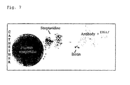
- bio-organic interactive material is bound to array surfaces using various strategies. These strategies include standard streptavidin-biotin interaction as shown in Figure 7 . It also includes the direct binding of (monoclonal) antibodies like IgG or fragments there of to the array surface via adhesion or electrostatic interaction. In addition, covalent linkage of target-specific molecular structures like antibodies or fragments there of, oligomers made of nucleic acids, or peptide or glycopeptides could be performed using linker technology as described in the detailed example below. The latter technique allows the precise binding of target specific molecules to nanoislands giving nanometer scale spatial resolution and therefore provides accurate real-time information regarding not only the concentration of a specific analyte but also its spatial distribution.
- the “Diagnostic-Nanosensor” is for medical application, for biological and biochemical research, as well as for environmental monitoring and protection and food safety. Concerning medical application, the “Diagnostic-Nanosensor” is assembled as a device for in vivo use.
- the "Diagnostic Nanosensor” is assembled on spring wire or stents giving a molecular or cell select catheter to obtain rare molecular or cellular components directly out of the circulation or the body in general ( Figure 9 ).
- the "Diagnostic-Nanosensor" assembled on e.g. spring wires or stents gives a cell or molecular select catheter which is useful for prenatal diagnosis of chromosomal aberrations, cancer diagnosis and the monitoring of chronic diseases like cancer, metabolic, infectious, allergic and inflammatory diseases.
- This device is applied as descript below.
- the "Diagnostic Nanosensor" is for the isolation of rare cells out of the peripheral blood, e.g. trophoblasts.
- Trophoblasts are foetal cells that appear in maternal blood around the 7 th gestational week at a concentration of about 1-2 per ml.
- the cell select catheter equipped with a monoclonal antibody that is directed against cellular but not soluble HLA-G binds specifically circulating trophoblasts in maternal blood.
- the number of bound cells to the cell select catheter depends on the retention period in the maternal circulation and the actual cell concentration. Appropriate numbers of trophoblasts for prenatal diagnoses of chromosomal aberration and other genetic defects could be collected after a retention period of 30 ⁇ 15 minutes in vivo. After replacing of the catheter the tip of the catheter with the attached cells is placed into a collector tube for transport to specialized laboratories.
- nanosized metallic particles show different optical absorption spectra depending on size.
- the surface plasmon band is due to collective electron oscillation around the surface of the particles.
- Ag (Silver) nanoparticles have plasmon band around 390 nm while Au nanoparticles have the plasmon band around 520 nm.
- the pick position, intensity and bandwidth of the surface plasmon absorption are directly related to size, morphology (shape), and surface functionality of the particles (see Figure 11 &12).
- the two-dimensional ordering of latex particles as a basis for nanosphere lithography (NSL) has been used by us and others in the past 1 , 2 , 3 , 4 , 5 , 6 , 7 , 8 .
- NSL nanosphere lithography
- the evaporation or sputtering of different materials through a latex particle mask enabled the production of lattices of triangular islands on various substrates, the shape of the islands being determined by the shape of the aperture between the spheres in the mask.
- the size of the aperture between the spheres depends on the size of the beads in the monolayer. To overcome this limitation, we annealed the monolayer to downsize the apertures in the mask from an initial 200 nm to 30 nm.
- Wiesendanger Appl. Phys. A 1996, 63, 617 . 6 R. Micheletto, H. Fukuda, M. Ohtsu, Langmuir 1995, 11, 3333 . 7 F. Burmeister, W. Badowsky, T. Braun, S. Wieprich, J. Boneberg, P. Griprich, Appl. Surf. Sci. 1999, 461, 144 . 8 N. D. Denkov, O. D. Velev, P. A. Kralchevsky, I. B. Ivanov, H. Yoshimura, K. Nagayama, Langmuir 1992, 8, 3183 .
- a piece of silicon, stainless steal, glass or sapphire substrate (1 cm 2 ) could be used for the deposition of polystyrene (PS) latex particles.
- PS polystyrene
- the amount of solution that could be distributed to cover the whole water surface with a hexagonal close packed (hcp) monolayer is limited by the size of the Petri dish and the diameter of the spheres. About 70% of this amount of solution is applied to the surface of the water, which left some places for stress relaxation and avoided the formation of cracks in the lattice during the next steps of the preparation.
- the monolayer has the biggest crystals of about 2 cm 2 , with very irregular shapes.
- gentle waves are applied to the liquid medium by slow and careful vessel tilting. After this treatment, crystals of about 25 cm 2 are created that show clear diffraction colors.
- the monolayer is deposited on a substrate by slow water evaporation.
- annealing of masks is performed.
- the monolayer of 540-nm PS latex nanospheres on a conductive Si substrate is immersed in a mixture (25 mL) of water/ethanol/acetone (3:1:1).
- Microwave heating is used up to the boiling temperature of the mixture, then additional microwave pulses are applied with duration of 3 s and period of 28 s.
- the increasing number of pulses causes gradual mask annealing and a decrease of the size of the apertures.
- the dependence of aperture morphology on number of pulses is presented in Figure 2 .
- the liquid environment of the sample ensured very homogeneous annealing-the feature sizes become uniform over the whole area of the sample.
- the control of the aperture size was very good and reproducible.
- Metal deposition is carried out by evaporation using an e-beam evaporator.
- the evaporation system is modified to ensure control over the evaporation angle (è) and the sample rotation at the same time ( Figure 4 ).
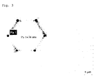
- FIG. 3 An annealed mask with 30-nm apertures ( Figure 3 ) is used for the fabrication of Co magnetic nanoparticles or Au nanoparticles in a honeycomb lattice.
- a layer of Co or Au is evaporated (10 nm at 0.01 nms -1 ) with the sample placed perpendicular to the evaporation beam.
- the result for Co particles is presented in Figure 5 .
- succinimidyl 6-[3'-(2-pyridyldithio)-propionamido] hexanoate, (a SPDP reagent) 12 in DMSO (dimethylsulfoxide) or ethanol was incubated with our periodic arrays of nanostructures in the presence of 150 mM DTT (dithiothreitol) for 30 minutes. This procedure allows covalent linkage of thiol to Au nanoislands.
- buffer PBS-EDTA
- the SPDP reagents produce disulfide-containing linkages that may be cleaved later with reducing agents such as dithiothreitol (DTT).
- DTT dithiothreitol
- the amine-reactive portion of SPDP reagents is the N- hydroxysuccinimide (NHS) ester. Reactions are most commonly performed in phosphate, carbonate/bicarbonate, or borate buffers at pH 7-8. Other buffers may be used provided they do not contain primary amines (or thiols or disulfide reducing reagent).
- the rate of reaction and degradation by hydrolysis increases with increasing pH; for example, the half-life of the NHS ester is several hours at pH 7 and less than 10 minutes at pH 9.
- NHS-ester reagents like SPDP and LC-SPDP have limited aqueous solubility and must be dissolved in organic solvent before adding them to a reaction mixture.
- Sulfo-NHS-ester reagents like Sulfo-LCSPDP are water-soluble and may be added directly to aqueous reaction mixtures.
- the sulfhydryl reactive portion of SPDP reagents is the 2-pyridyldithio group, which reacts optimally with sulfhydryls between pH 7 and 8.
- reaction buffers must be free of thiols and disulfide reducing agents until quenching or reduction of the 2-pyridyl disulfide is desired.
- Two basic strategies may be used to form cleavable cross-links between proteins with SPDP reagents, depending whether one or neither protein already possesses sulfhydryl groups (-SH) in addition to primary amines. Both conjugation methods result in cross-links that contain a disulfide bond in the spacer arm, which may be cleaved by reduction with dithiothreitol (DTT) or other reducing agent.
- DTT dithiothreitol
- cross-links created using SPDP reagents can be cleaved with 25 mM DTT at pH 4.5 without reducing native protein disulfide bonds. However, when preservation of native disulfide bonds is not a concern, cleavage with DTT may be performed most efficiently at pH 7-9.
- Cross-linking experiments with SPDP reagents are not limited to those involving proteins. Any of a variety of molecules with primary amines (-NH2) and sulfhydryl groups may be modified or crosslinked using an SPDP reagent.
Landscapes
- Health & Medical Sciences (AREA)
- Life Sciences & Earth Sciences (AREA)
- Immunology (AREA)
- Engineering & Computer Science (AREA)
- Chemical & Material Sciences (AREA)
- Biomedical Technology (AREA)
- Urology & Nephrology (AREA)
- Biochemistry (AREA)
- General Health & Medical Sciences (AREA)
- General Physics & Mathematics (AREA)
- Physics & Mathematics (AREA)
- Pathology (AREA)
- Analytical Chemistry (AREA)
- Molecular Biology (AREA)
- Hematology (AREA)
- Cell Biology (AREA)
- Microbiology (AREA)
- Biotechnology (AREA)
- Nanotechnology (AREA)
- Food Science & Technology (AREA)
- Medicinal Chemistry (AREA)
- Investigating Or Analyzing Materials By The Use Of Magnetic Means (AREA)
- Soft Magnetic Materials (AREA)
- Investigating Or Analysing Materials By Optical Means (AREA)
- Apparatus Associated With Microorganisms And Enzymes (AREA)
Abstract
Description
- This invention relates generally to biosensor technology, and pertains more particularly to novel multifunctional biosensors based on ordered arrays of metallic, semiconductors and magnetic nano-islands for medical, biological, biochemical, chemical and environmental applications.
- Specifically, the present invention relates to a Diagnostic Nanosensor according to
claim 1. -
FR 2 860 872 A - The nanoscale science and engineering have shown great promise for the fabrication of novel biosensors with faster response and higher sensitivity than that of planar sensor configurations, due to their small dimensions combined with a dramatically increased contact surface and strong binding with biological and chemical reagents. Such biosensors have important applications in medicine, in biological and biochemical research, as well as for environmental monitoring and protection and in food industry.
-
WO2004/086044 discloses the production of nanosensors based on silver nanoparticles. The use of nanosphere lithography is mentioned. - The invention in its broadest form is defined by independent claim 1:
- A Diagnostic-Nanosensor that is assembled on a spring wire or catheter or stent and that can be used under in vivo conditions, comprising:
- a) a deposition of nanopatterned islands of metal on planar or non-planar, transparent or non-transparent surfaces, said nanopatterned islands comprising a nanostructured periodic array of metallic nanoislands assembled of a various morphology and made up of noble metals, wherein the metallic nanoislands are produced by nanosphere lithography,
- b) subsequent deposition of bio-organic interactive material on the deposition described under a) to give a sandwich device for interacting with organic or inorganic targets.
substances and lead to an increase in sensitivity of the nano-biosensor in terms of lower limit and dynamic range of detention.
- It is the primary objective of this invention to address the novel multifunctional biosensor technology based on metallic semiconductors and magnetic nanoislands and nanoisland arrays giving a new nanosensor for diagnostic purposes in medicine, biological and biochemical research, as well as in environmental monitoring and protection and in food industry. The surface of nanoparticles can be functionalized with bio-organic interactive material that due to their specificity interact selectively with other molecules. By chemically controlling the surface of the nanoparticles, they can be "programmed" to recognize and selectively bind molecules, other nanoparticles (semiconductors) or a suitably patterned substrate surface like the cellular outer membrane.
Particularly, it is an objective of this invention to provide nano-transducers based on noble metal nanoislands through resonant excitations of the collective oscillations of the conduction electrons on the nanoislands, the so-called surface plasmon resonances. This phenomenon can be coupled to the binding event between receptors and their targets. Highly improved electrical conductivity of these nano-transducers translate into unprecedented sensitivity and enable the design of novel sensing devices for the detection of pathogens and toxins of concern, to homeland security, food safety, environmental quality, and public health. The use of noble metallic nanoislands results in increased signal transduction of the binding event between bio-organic interactive material and their target substances and lead to an increase in sensitivity of the nano-biosensor in terms of lower limit and dynamic range of detection. - In order to solve the above-defined objects, the present invention provides the Diagnostic Nanosensor according to
claim 1. - Preferred embodiments are claimed in the subclaims.
- A highly periodic array of metallic nanoislands acting as nanotranducers forms a new integral structure called a "Diagnostic-Nanosensor". This "Diagnostic-Nanosensor" is deposited on a device that could have a form like a needle or wire or tube or chip and made out of transparent (glass, sapphire) or non-transparent material (silicon substrates, stainless steel, biocompatible polymers). The "Diagnostic-Nanosensor" is made by using nanosphere lithography (NSL) to create metallic nanoislands. This technique allows the total control of size and shape of the functional part of the nanosensor.
- One important feature in the optical spectra of nanoislands or nanosized metal particles (Ag, silver; Au, gold) is the surface plasmon band. The surface plasmon band is due to collective electron oscillation around the surface mode of the particles. For example Ag nanoparticles have a strong absorption around 390 nm while Au nanoparticles have the plasmon band around 520 nm. The peak position and bandwidth of the surface plasmon absorption are related to the size and shape. For gold nanorods, however the absorption spectrum changes dramatically and a bimodal spectrum can be detected with peak position dependent on the aspect ratio of the nanorods.
- The subsequent modification of nanostructured surfaces of a catheter or spring wire or stent with bio-organic interactive material is presented as an example in
Figure 9 . This step and especially the binding of DNA, other molecules or cells on the particles surfaces leads to a change in the dielectric constant of this system and can easily be detected by the optical method. The Diagnostic Nanosensor achieves nanometer scale spatial resolution and therefore provides accurate real-time information regarding not only the concentration of a specific analyte of organic or inorganic nature but also its spatial distribution. The operation of sensors made with nanowires, nanotubes, or nano-contacts is based mostly on the reversible change in the optical and electronic properties
In general the sensitivity and specification of the Diagnostic-Nanosensor according to the invention is based on quantum size effect and can be occur with the decreasing the size of our nanoparticles.
The "Diagnostic-Nanosensor" of this invention may be used to detect biological materials, such as proteins, carbohydrates, or nucleic acids or cells as well as non-biological materials, such as synthetic polymers or non organic nanoparticles. The "Diagnostic-Nanosensor" could be used under in vivo as well as in vitro conditions. - In the biomedical and human area there is a need for better detection and diagnosis. The nanoscale materials are insatiable for producing new detection and diagnostic devices. On the nanometer length scale, materials exhibit new properties such quantum size confinement. Their surface properties become increasingly important. Nanoparticles made of metals (gold, silver, etc), semiconductors (CdS, CdTe, CdSe, Si, etc) or (superpara-) magnetic particles form an ideal platform for functionalized nanoscale materials. The particles size can be varied from some of nanometer to 100 nm. The small particle size implies high sensitivity and selectivity if they could further functionalized by the precise deposition of bio-organic interactive material for the binding of a given analyte.
The "Diagnostic-Nanosensor" according to the invention is made by using nanosphere lithography (NSL) to create metallic nanoislands. This technique allows the total control of size and shape of the functional part of the nanosensor down to sizes below 10 nm. Subsequent depositions of bio-organic interactive material on the nanostructures give a sandwich device for interacting with organic or inorganic targets. Because the sensitivity and specification of any biosensor depends on the size of a given sensor unit, the invention descript here allows sensitivities far below the pmol range. In general, the Diagnostic-Nanosensor according to the invention is based on quantum size effect and can be tuned with decreasing the size of utilized nanoparticles that are deposited on various support materials and are subsequently functionalized with bio-organic interactive material to give a sandwich device for interacting with organic or inorganic targets.
Assembling the "Diagnostic Nanosensor" on biocompatible supports like spring wire or catheter or stent material as used in medicine the "Diagnostic Nanosensor" gives a molecular/cell select catheter that could be applied for in vivo diagnostic purposes. As such the "Diagnostic Nanosensor" according to the invention is for the direct detection and isolation of rare molecules or cells out of the peripheral blood or the body. This application technique enables diagnostic procedures that were not possible before: prenatal diagnoses of chromosomal aberration using foetal trophoblasts present in maternal circulation; cancer diagnoses and monitoring of cancer therapy based on the detection of disseminated cancer cells in the body.
The "Diagnostic Nanosensor" according to the invention allows detection of a resultant interaction between the bio-organic interactive material and the target substance by measuring the collective oscillations of the conduction electrons on the nanoislands, the so called surface plasmon resonance, or detection of optical properties from semiconductors particles (luminescence), or the super-paramagnetic properties by magnetic particles. These detection methods enable the use of the "Diagnostic Nanosensor" according to the invention on scene, i.e. without the infrastructure of a laboratory. Thus, the "Diagnostic Nanosensor" could be used at the bedside, in the operating theatre, in the ambulance, and on battle field. - The surface treatment of various supports with NSL and subsequent functionalizing of the obtained nanostructured array with bio-organic interactive material leads to surprising results
- The methods for producing the diagnostic-nanosensor comprise two separate but interrelated procedures:
- (1) The production of periodic arrays of nanostructures.
- (2) Functionalizing nanostructured arrays using bioorganic interactive material that could be bound to the arrays directly or indirectly through linker technologies.
- To produce periodic arrays of nanostructures, a relatively inexpensive and simple method of nanoparticles or nanospheres lithography (NSL) will be used for the creation of periodic and quasi-periodic self assembly spherical objects like polystyrene or silica particles with a diameter in the range of 200 to 2000 nm (
Figure 1a ). The two and three-dimensional (2-D, 3-D) ordered particles will be used as a mask for the following deposition of various amounts of different metals (Au, Ag, Pt) or semiconductors (CdS, CdTe, CdSe). After the evaporation process the liftoff of the mask will be performed. The metallic 2-D (Figure 1b ) or3-D varying particle arrays permit the control of the distance between the nanoparticles as well as their cubic, hexagonal or more complicated ordering. The amount of the deposited materials through the mask can determine directly their optical and electronic properties. - The production of periodic arrays of nanostructures involves the following steps:
- a) Production of a two dimensional mask that consists of spherical monodisperse polystyrene particles of sizes from 200 nm to 7000 nm. This production involves the controlled aggregation of the particles between solvents of different surface behaviour for the precise structuring of the two dimensional mask. The final morphology of the mask is determined using temperature and mechanical treatment to give triangles, roots, dots or others.
- b) Deposition of the mask on planar substrates (plates or chip) or non-planar substrates (catheters, spring wires, stents). The substrates could be biocompatible for in vivo applications of the sensor.
- c) Evaporation of noble metals, semiconductors or magnetic materials (gold, platinum, silver, CdSe, CdTe, Cobalt, Nickel) through the mask.
- d) Dissolving the mask by temperature or chemical treatment.
- To functionalize nanostructured arrays, bio-organic interactive material is bound to array surfaces using various strategies. These strategies include standard streptavidin-biotin interaction as shown in
Figure 7 . It also includes the direct binding of (monoclonal) antibodies like IgG or fragments there of to the array surface via adhesion or electrostatic interaction. In addition, covalent linkage of target-specific molecular structures like antibodies or fragments there of, oligomers made of nucleic acids, or peptide or glycopeptides could be performed using linker technology as described in the detailed example below. The latter technique allows the precise binding of target specific molecules to nanoislands giving nanometer scale spatial resolution and therefore provides accurate real-time information regarding not only the concentration of a specific analyte but also its spatial distribution. - The "Diagnostic-Nanosensor" is for medical application, for biological and biochemical research, as well as for environmental monitoring and protection and food safety. Concerning medical application, the "Diagnostic-Nanosensor" is assembled as a device for in vivo use.
- For the in vivo device the "Diagnostic Nanosensor" is assembled on spring wire or stents giving a molecular or cell select catheter to obtain rare molecular or cellular components directly out of the circulation or the body in general (
Figure 9 ). - As device for in vivo appliance the "Diagnostic-Nanosensor" assembled on e.g. spring wires or stents gives a cell or molecular select catheter which is useful for prenatal diagnosis of chromosomal aberrations, cancer diagnosis and the monitoring of chronic diseases like cancer, metabolic, infectious, allergic and inflammatory diseases. This device is applied as descript below.
- a) Puncture of a blood vessel (vein or artery) using a hollow needle.
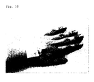
- b) Putting the nanosensor through the hollow needle or through a standard venous line into the blood vessel as shown in
Figure 10 . - c) Replacing the needle but keeping the nanosensor in place.
- d) After the appropriate incubation time (between 5 to 60 minutes) the nanosensor is replaced with the attached cells and/or molecules for further processing.
- As a cell select catheter the "Diagnostic Nanosensor" according to the invention is for the isolation of rare cells out of the peripheral blood, e.g. trophoblasts. Trophoblasts are foetal cells that appear in maternal blood around the 7th gestational week at a concentration of about 1-2 per ml. The cell select catheter equipped with a monoclonal antibody that is directed against cellular but not soluble HLA-G binds specifically circulating trophoblasts in maternal blood. The number of bound cells to the cell select catheter depends on the retention period in the maternal circulation and the actual cell concentration. Appropriate numbers of trophoblasts for prenatal diagnoses of chromosomal aberration and other genetic defects could be collected after a retention period of 30±15 minutes in vivo. After replacing of the catheter the tip of the catheter with the attached cells is placed into a collector tube for transport to specialized laboratories.
- According to the quantum size confinement effect nanosized metallic particles show different optical absorption spectra depending on size. The surface plasmon band is due to collective electron oscillation around the surface of the particles. For example Ag (Silver) nanoparticles have plasmon band around 390 nm while Au nanoparticles have the plasmon band around 520 nm. The pick position, intensity and bandwidth of the surface plasmon absorption are directly related to size, morphology (shape), and surface functionality of the particles (see
Figure 11 &12). - By covering the 2-dimensional assemblies of gold nanoparticles with avidin their plasmon peak shifts toward longer wavelength and can be easily detected as shown in
Fig. 12 . - The invention may be further illustrated by the following examples:
- The two-dimensional ordering of latex particles as a basis for nanosphere lithography (NSL) has been used by us and others in the past1,2,3,4,5,6,7,8. The evaporation or sputtering of different materials through a latex particle mask enabled the production of lattices of triangular islands on various substrates, the shape of the islands being determined by the shape of the aperture between the spheres in the mask. Clearly, the size of the aperture between the spheres depends on the size of the beads in the monolayer. To overcome this limitation, we annealed the monolayer to downsize the apertures in the mask from an initial 200 nm to 30 nm. This result was far beyond our expectations, and was essential for the fabrication of nanodot particles (
Figure 5 ) and isolated nanorings (Figure 6 ).
1 H.W. Deckman, J. H. Dunsmir, Appl. Phys. Lett. 1982, 41, 377.
2 M. Giersig, P. Mulvaney, Langmuir 1993, 9, 3408.
3 H.W. Deckman, J. H. Dunsmuir, Appl. Phys. Lett. 1982, 4, 377.
4 J. C. Hulteen, R. P. Van Duyne, J. Vac. Sci. Technol. A 1995, 13, 1553.
5 M. Winzer, M. Kleiber, N. Dix, R. Wiesendanger, Appl. Phys. A 1996, 63, 617.
6 R. Micheletto, H. Fukuda, M. Ohtsu, Langmuir 1995, 11, 3333.
7 F. Burmeister, W. Badowsky, T. Braun, S. Wieprich, J. Boneberg, P. Leiderer, Appl. Surf. Sci. 1999, 461, 144.
8 N. D. Denkov, O. D. Velev, P. A. Kralchevsky, I. B. Ivanov, H. Yoshimura, K. Nagayama, . - In our recent work we demonstrated that if the sample is moving during the deposition process, the evaporated structures can become much more complex and range from cuplike structures to rods and wires.9 Now, we improved our technique further. Improvements involve decreasing the size of the apertures between particles by temperature treatment applied to the nanosphere mask before the evaporation process, and using different material in nanometer size for the deposition on various supports.9
A. Kosiorek, W. Kandulski, P. Chudzinski, K. Kempa, M. Giersig, Nano Lett. 2004, 4, 1359. - A piece of silicon, stainless steal, glass or sapphire substrate (1 cm2) could be used for the deposition of polystyrene (PS) latex particles. In this first step, the latex particles (diameter=540 nm) in ethanol/water solution are slowly applied to the surface of water in a 15 cm Petri dish using a glass pipette. The amount of solution that could be distributed to cover the whole water surface with a hexagonal close packed (hcp) monolayer is limited by the size of the Petri dish and the diameter of the spheres. About 70% of this amount of solution is applied to the surface of the water, which left some places for stress relaxation and avoided the formation of cracks in the lattice during the next steps of the preparation. At this stage the monolayer has the biggest crystals of about 2 cm2, with very irregular shapes. To promote the growth of large crystals, gentle waves are applied to the liquid medium by slow and careful vessel tilting. After this treatment, crystals of about 25 cm2 are created that show clear diffraction colors. Finally, the monolayer is deposited on a substrate by slow water evaporation.
- After the drying process, annealing of masks is performed. The monolayer of 540-nm PS latex nanospheres on a conductive Si substrate is immersed in a mixture (25 mL) of water/ethanol/acetone (3:1:1). Microwave heating is used up to the boiling temperature of the mixture, then additional microwave pulses are applied with duration of 3 s and period of 28 s. The increasing number of pulses causes gradual mask annealing and a decrease of the size of the apertures. The dependence of aperture morphology on number of pulses is presented in
Figure 2 . The liquid environment of the sample ensured very homogeneous annealing-the feature sizes become uniform over the whole area of the sample. The control of the aperture size was very good and reproducible. With the 540-nm PS latex monolayer we were able to adjust the aperture size from an initial 200 nm to 25 nm (Figures 2 and3 ). The annealed masks have different thicknesses-the more the sample is annealed, the flatter and thinner it is. - Metal deposition is carried out by evaporation using an e-beam evaporator. The evaporation system is modified to ensure control over the evaporation angle (è) and the sample rotation at the same time (
Figure 4 ). - An annealed mask with 30-nm apertures (
Figure 3 ) is used for the fabrication of Co magnetic nanoparticles or Au nanoparticles in a honeycomb lattice. A layer of Co or Au is evaporated (10 nm at 0.01 nms-1) with the sample placed perpendicular to the evaporation beam. The result for Co particles is presented inFigure 5 . The size of the Co nanodot particles varies in a small regime and some of them are missing. These differences are all over the sample and arise during the annealing process, most probably because of the small differences (CV=2.4%) in PS sphere diameters. - We used similar masks for nanoring fabrication. In this experiment Fe was deposited (100 nm) through the annealed template from
Figure 3 at the evaporation angle θ=258, and the sample was rotated during deposition. The rings had uniform outer (~150 nm) and inner (~100 nm) diameters (inset ofFigure 6 ), which could be controlled by altering the evaporation angle. The thickness of the rings inFigure 6 is about 7 nm and can also be controlled by altering the aperture size of the nanosphere mask and the amount of deposited metal. In a previous paper, we discussed the relationship between the evaporation angle and the amount of deposited metal. Recently there have been many attempts to fabricate nanorings.1011 However, our method combines a very good control of the dimensions of the structures and fabrication materials with the reproducibility and simplicity of the preparation process.
10 F. Yan, W. A. Goedel, Nano Lett. 2004, 4, 1193.
11 J. McLellan, M. Geissler, Y. Xia, J. Am. Chem. Soc. 2004, 126, 10830. - We used the following strategy to specifically bind monoclonal IgG to Au nanoislands that were assembled on transparent or non-transparent substrates.
- A 20 mM solution of succinimidyl 6-[3'-(2-pyridyldithio)-propionamido] hexanoate, (a SPDP reagent)12 in DMSO (dimethylsulfoxide) or ethanol was incubated with our periodic arrays of nanostructures in the presence of 150 mM DTT (dithiothreitol) for 30 minutes. This procedure allows covalent linkage of thiol to Au nanoislands.
After cleaning the arrays with buffer (PBS-EDTA) bioorganic interactive material at concentrations from 0.5 to 2 mg/ml was incubated with the array for 1 h or over night. We revealed coatings as shown inFigure 8 for the case that monoclonal IgG at a concentration of 1 mg/ml was used. The dimension of a single dot spot on gold is 12 nm, corresponding to the average molecular weight of a single IgG molecule of 150 kD.
12 N-succinimidyl 3-(2-pyridyldithio) propionate (SPDP reagents) are a unique group of amine- and sulfhydryl-reactive heterobifunctional cross-linkers. Whether they are used to form amine-to-amine or amine-to-sulfhydryl cross-links among molecules, the SPDP reagents produce disulfide-containing linkages that may be cleaved later with reducing agents such as dithiothreitol (DTT). The amine-reactive portion of SPDP reagents is the N-hydroxysuccinimide (NHS) ester. Reactions are most commonly performed in phosphate, carbonate/bicarbonate, or borate buffers at pH 7-8. Other buffers may be used provided they do not contain primary amines (or thiols or disulfide reducing reagent). The rate of reaction and degradation by hydrolysis increases with increasing pH; for example, the half-life of the NHS ester is several hours at pH 7 and less than 10 minutes at pH 9. NHS-ester reagents like SPDP and LC-SPDP have limited aqueous solubility and must be dissolved in organic solvent before adding them to a reaction mixture. Sulfo-NHS-ester reagents like Sulfo-LCSPDP are water-soluble and may be added directly to aqueous reaction mixtures.
The sulfhydryl reactive portion of SPDP reagents is the 2-pyridyldithio group, which reacts optimally with sulfhydryls betweenpH 7 and 8. The reaction results in displacement of a pyridine-2-thione group, the concentration of which may be determined by measuring the absorbance at 343 nm. Reaction buffers must be free of thiols and disulfide reducing agents until quenching or reduction of the 2-pyridyl disulfide is desired. Two basic strategies may be used to form cleavable cross-links between proteins with SPDP reagents, depending whether one or neither protein already possesses sulfhydryl groups (-SH) in addition to primary amines. Both conjugation methods result in cross-links that contain a disulfide bond in the spacer arm, which may be cleaved by reduction with dithiothreitol (DTT) or other reducing agent. In most cases, cross-links created using SPDP reagents can be cleaved with 25 mM DTT at pH 4.5 without reducing native protein disulfide bonds. However, when preservation of native disulfide bonds is not a concern, cleavage with DTT may be performed most efficiently at pH 7-9. Cross-linking experiments with SPDP reagents are not limited to those involving proteins. Any of a variety of molecules with primary amines (-NH2) and sulfhydryl groups may be modified or crosslinked using an SPDP reagent. -
- Figure 1:
- Schematic illustration (a) and typical AFM image (b) of gold nanoparticles after evaporation process and liftoff of the mask
- Figure 2:
- A 540-nm PS latex mask annealed in 25 mL of water/EtOH/acetone mixture by A) 1,
B) 2, C) 4, D) 6, E) 7, and F) 10 microwave pulses. - Figure 3:
- SEM image of the annealed 540-nm PS latex mask with sizes of all apertures below 50 nm.
- Figure 4:
- Diagram of the modified evaporation system: 1) sample holder, 2) evaporation source, 3) crucible, 4) water cooling system, 5) electron beam source, 6) shutter, 7) magnetic field. θ is the evaporation angle and α is the rotation angle of the sample.
- Figure 5:
- Ordered spherical Co nanoparticles evaporated through an annealed 540-nm PS latex mask. The diameter of a single particle is approximately 30 nm.
- Figure 6:
- SEM picture of ordered Fe nanorings evaporated through an annealed 540-nm PS latex mask. The outer diameter of the single ring is 150 nm and the width of the ring is 20-30 nm.
- Figure 7:
- Graphic presentation of how DNA or cellular structures are detected by specific antibodies. Antibodies are cross linked through streptavidin-biotin to Au-nanoparticles. Au-nanoparticles decorate the nanostructured surface of a catheter or spring wire or stent. This technique is the first nano-sandwich approach for the production of a Diagnostic Nanosensor.
- Figure 8:
- IgG molecules covalently tethered to Au nanoislands through SPDP linker. The diameter of a single dot is 12 nm, corresponding to the average molecular weight of IgG (150 kD).
- Figure 9:
- Diagnostic nanosensors assembled on spring wire to give a cell or molecular select catheter.
- Figure 10:
- Cell select catheter in place. A spring wire with diagnostic nanosensors assembled on its surface is put into a peripheral vein through a standard venous line. After appropriate incubation time the cell select catheter is replaced with rare molecules or cells of interest attached to its surface for further laboratory analyses.
- Figure 11:
- Influence of particle size on plasmon resonance. Different size of the mask (380, 540, 980, or 1710 nm) gives correspondent nanoparticle depositions on transparent substrate that generate typical spectra.
- Figure 12:
- Typical example of spectrum changes of the plasmon resonance after deposition of bio-interactive material (avidin in this case) on nanostructured arrays.
Claims (11)
- A Diagnostic-Nanosensor that is assembled on a spring wire or catheter or stent and that can be used under in vivo conditions, comprising:a) a deposition of nanopatterned islands of metal on planar or non-planar, transparent or non-transparent surfaces, said nanopatterned islands comprising a nanostructured periodic array of metallic nanoislands assembled of a various morphology and made up of noble metals, wherein the metallic nanoislands are produced by nanosphere lithography,b) subsequent deposition of bio-organic interactive material on the deposition described under a) to give a sandwich device for interacting with organic or inorganic targets.
- Diagnostic-Nanosensor according to claim 1, wherein said nanostructured periodic array of metallic nanoislands is assembled of nano-needles, wires, tubes, rings or spheres.
- Diagnostic-Nanosensor according to claim 1 or 2, wherein the said metallic-islands are made up of the noble metals gold, platinum, and silver.
- The Diagnostic-Nanosensor of one of the preceding claims, wherein the said planar or non-planar substrate is made of stainless steel, glass, silicon or biocompatible polymers and could be in general transparent, non-transparent, conductive, or non-conductive.
- The Diagnostic-Nanosensor of the preceding claims, wherein the said bio-organic interactive material could be antibodies or part of antibodies, peptides, oligomers made of nucleic acids, or in general receptor structured organic or inorganic compounds that specifically interact with targets.
- The Diagnostic-Nanosensor according to one of the preceding claims, wherein the nanosphere lithography enable the creation of monodisperse, surface-confined metallic nanotriangles.
- The Diagnostic-Nanosensor according to one of the preceding claims, wherein the bio-organic interactive material is linked to the nanopatterned structures through adhesion, electrostatic interaction, chemically linkage, or covalent or non-covalent binding.
- The Diagnostic-Nanosensor according to one of the preceding claims, wherein the binding of target substance to the bioconjugated metallic surface induces a collective interaction with the surface electron (plasmon resonance).
- The Diagnostic-Nanosensor according to one of the preceding claims, wherein the binding of target substance to the bioconjugated semiconductor surface creates an exiton interaction which could be detected by measuring luminescence or fluorescence.
- The Diagnostic-Nanosensor according to one of the preceding claims, wherein the binding of target substance to the bioconjugated magnetic surface can be measured by the interaction between ferro- and/or superparamagnetic materials.
- The Diagnostic-Nanosensor according to one of the preceding claims, wherein every metallic or non-metallic nanoislands act as individual sensor.
Priority Applications (11)
| Application Number | Priority Date | Filing Date | Title |
|---|---|---|---|
| AT06090012T ATE520030T1 (en) | 2006-01-19 | 2006-01-19 | DIAGNOSTIC NANOSENSOR AND ITS USE |
| EP06090012A EP1811302B1 (en) | 2006-01-19 | 2006-01-19 | Diagnostic nanosensor and its use in medicine |
| CA002609573A CA2609573A1 (en) | 2005-06-10 | 2006-06-09 | Diagnostic-nanosensor and its use in medicine |
| US11/917,032 US8846580B2 (en) | 2005-06-10 | 2006-06-09 | Diagnostic nanosensor and its use in medicine |
| AT06743163T ATE519110T1 (en) | 2005-06-10 | 2006-06-09 | DIAGNOSTIC NANOSENSOR AND ITS USE IN MEDICINE |
| BRPI0611821-6A BRPI0611821A2 (en) | 2005-06-10 | 2006-06-09 | diagnostic nanosensor, method to produce it, use of it, detection method |
| CN2006800204055A CN101305280B (en) | 2005-06-10 | 2006-06-09 | Diagnostic-nanosensor and its use in medicine |
| AU2006256859A AU2006256859B2 (en) | 2005-06-10 | 2006-06-09 | Diagnostic-nanosensor and its use in medicine |
| PCT/EP2006/005760 WO2006131400A1 (en) | 2005-06-10 | 2006-06-09 | Diagnostic-nanosensor and its use in medicine |
| EP06743163A EP1907848B1 (en) | 2005-06-10 | 2006-06-09 | Diagnostic-nanosensor and its use in medicine |
| US11/733,834 US8197756B2 (en) | 2005-06-10 | 2007-04-11 | Diagnostic-nanosensor and its use in medicine |
Applications Claiming Priority (1)
| Application Number | Priority Date | Filing Date | Title |
|---|---|---|---|
| EP06090012A EP1811302B1 (en) | 2006-01-19 | 2006-01-19 | Diagnostic nanosensor and its use in medicine |
Publications (2)
| Publication Number | Publication Date |
|---|---|
| EP1811302A1 EP1811302A1 (en) | 2007-07-25 |
| EP1811302B1 true EP1811302B1 (en) | 2011-08-10 |
Family
ID=36337354
Family Applications (1)
| Application Number | Title | Priority Date | Filing Date |
|---|---|---|---|
| EP06090012A Expired - Lifetime EP1811302B1 (en) | 2005-06-10 | 2006-01-19 | Diagnostic nanosensor and its use in medicine |
Country Status (2)
| Country | Link |
|---|---|
| EP (1) | EP1811302B1 (en) |
| AT (1) | ATE520030T1 (en) |
Cited By (1)
| Publication number | Priority date | Publication date | Assignee | Title |
|---|---|---|---|---|
| EP2842578A1 (en) | 2013-08-27 | 2015-03-04 | GILUPI GmbH | Diagnostic device for the detection of disease related target structures |
Families Citing this family (4)
| Publication number | Priority date | Publication date | Assignee | Title |
|---|---|---|---|---|
| DE102008027095A1 (en) | 2008-06-06 | 2009-12-17 | Siemens Aktiengesellschaft | Intervention device for collecting biological material and method for its production |
| DE102008039798A1 (en) * | 2008-08-15 | 2010-02-25 | NMI Naturwissenschaftliches und Medizinisches Institut an der Universität Tübingen | Method of transferring nanostructures into a substrate |
| EP2430425A4 (en) * | 2009-05-12 | 2015-02-25 | Jean-François Masson | High sensitivity plasmonic structures for use in surface plasmon resonance sensors and method of fabrication thereof |
| US12290844B2 (en) | 2021-04-07 | 2025-05-06 | Identinano Ab | Method for sorting of items and an assembly for categorizing an item |
Family Cites Families (7)
| Publication number | Priority date | Publication date | Assignee | Title |
|---|---|---|---|---|
| US20020111551A1 (en) * | 2000-11-30 | 2002-08-15 | Erlach Julian Van | Method for detecting body condition using nano and microdevices |
| EP1608975B1 (en) * | 2003-03-28 | 2013-06-19 | The Provost, Fellows, Foundation Scholars, & the other members of Board, of the College of the Holy & Undiv. Trinity of Queen Elizabeth near Dublin | Sensor for detecting an analyte using silver nanoparticles |
| EP1623203A4 (en) * | 2003-05-14 | 2010-11-24 | Nantero Inc | Sensor platform using a non-horizontally oriented nanotube element |
| EP1680353A4 (en) * | 2003-09-18 | 2012-04-11 | Nanomix Inc | Nanostructures with electrodeposited nanoparticles |
| FR2860872A1 (en) | 2003-10-09 | 2005-04-15 | Commissariat Energie Atomique | MICRO-SENSORS AND NANO-SENSORS OF CHEMICAL AND BIOLOGICAL SPECIES WITH SURFACE PLASMONS |
| KR100578747B1 (en) * | 2003-12-26 | 2006-05-12 | 한국전자통신연구원 | Metal nanoparticle chemical sensors and sensor arrays encapsulated by mixed ligands |
| WO2005093831A1 (en) * | 2004-02-13 | 2005-10-06 | President And Fellows Of Harvard College | Nanostructures containing metal-semiconductor compounds |
-
2006
- 2006-01-19 AT AT06090012T patent/ATE520030T1/en not_active IP Right Cessation
- 2006-01-19 EP EP06090012A patent/EP1811302B1/en not_active Expired - Lifetime
Cited By (1)
| Publication number | Priority date | Publication date | Assignee | Title |
|---|---|---|---|---|
| EP2842578A1 (en) | 2013-08-27 | 2015-03-04 | GILUPI GmbH | Diagnostic device for the detection of disease related target structures |
Also Published As
| Publication number | Publication date |
|---|---|
| EP1811302A1 (en) | 2007-07-25 |
| ATE520030T1 (en) | 2011-08-15 |
Similar Documents
| Publication | Publication Date | Title |
|---|---|---|
| EP1907848B1 (en) | Diagnostic-nanosensor and its use in medicine | |
| Liang et al. | Carbon-based SERS biosensor: From substrate design to sensing and bioapplication | |
| Fateixa et al. | Hybrid nanostructures for SERS: materials development and chemical detection | |
| Pierrat et al. | Self-assembly of small gold colloids with functionalized gold nanorods | |
| Zeng et al. | A review on functionalized gold nanoparticles for biosensing applications | |
| Alex et al. | Functionalized gold nanoparticles: synthesis, properties and applications—a review | |
| Riboh et al. | A nanoscale optical biosensor: real-time immunoassay in physiological buffer enabled by improved nanoparticle adhesion | |
| Yang et al. | Fabrication of a flexible gold nanorod polymer metafilm via a phase transfer method as a SERS substrate for detecting food contaminants | |
| Smith et al. | Quantitative analysis of thiolated ligand exchange on gold nanoparticles monitored by 1H NMR spectroscopy | |
| Mayer et al. | A label-free immunoassay based upon localized surface plasmon resonance of gold nanorods | |
| Haes et al. | Solution-phase, triangular Ag nanotriangles fabricated by nanosphere lithography | |
| Frasconi et al. | Multifunctional Au nanoparticle dendrimer-based surface plasmon resonance biosensor and its application for improved insulin detection | |
| Huo | A perspective on bioconjugated nanoparticles and quantum dots | |
| Zhang et al. | Synthesis, properties, and optical applications of noble metal nanoparticle-biomolecule conjugates | |
| Zhang et al. | Enhancing sensitivity of surface plasmon resonance biosensor by Ag nanocubes/chitosan composite for the detection of mouse IgG | |
| KR102365091B1 (en) | Raman-active Nanoparticle for Surface Enhanced Raman Scattering and the Fabrication Method Thereof | |
| Mannelli et al. | Recent advances in analytical and bioanalysis applications of noble metal nanorods | |
| Liu et al. | Gold nanotubes: synthesis, properties and biomedical applications | |
| Ceja-Fdez et al. | Glucose detection using SERS with multi-branched gold nanostructures in aqueous medium | |
| Yeom et al. | Nanostructures in biosensor-a review | |
| de la Chapelle et al. | Nanoantenna | |
| Rajaeian et al. | Improved albumin detection in bovine serum albumin concentration by Au/Ag nanocrystallites | |
| EP1811302A1 (en) | Diagnostic nanosensor and its use in medicine | |
| Chen et al. | Synthesis of gold nanoparticles and functionalization with DNA for bioanalytical applications | |
| Khlebtsov et al. | Plasmonic Nanoparticles: Fabrication, Optical Properties, and Biomedical Applica-tions |
Legal Events
| Date | Code | Title | Description |
|---|---|---|---|
| PUAI | Public reference made under article 153(3) epc to a published international application that has entered the european phase |
Free format text: ORIGINAL CODE: 0009012 |
|
| AK | Designated contracting states |
Kind code of ref document: A1 Designated state(s): AT BE BG CH CY CZ DE DK EE ES FI FR GB GR HU IE IS IT LI LT LU LV MC NL PL PT RO SE SI SK TR |
|
| AX | Request for extension of the european patent |
Extension state: AL BA HR MK YU |
|
| RAP1 | Party data changed (applicant data changed or rights of an application transferred) |
Owner name: GILUPI GMBH |
|
| 17P | Request for examination filed |
Effective date: 20080128 |
|
| AKX | Designation fees paid |
Designated state(s): AT BE BG CH CY CZ DE DK EE ES FI FR GB GR HU IE IS IT LI LT LU LV MC NL PL PT RO SE SI SK TR |
|
| 17Q | First examination report despatched |
Effective date: 20080328 |
|
| GRAP | Despatch of communication of intention to grant a patent |
Free format text: ORIGINAL CODE: EPIDOSNIGR1 |
|
| GRAS | Grant fee paid |
Free format text: ORIGINAL CODE: EPIDOSNIGR3 |
|
| GRAA | (expected) grant |
Free format text: ORIGINAL CODE: 0009210 |
|
| AK | Designated contracting states |
Kind code of ref document: B1 Designated state(s): AT BE BG CH CY CZ DE DK EE ES FI FR GB GR HU IE IS IT LI LT LU LV MC NL PL PT RO SE SI SK TR |
|
| REG | Reference to a national code |
Ref country code: GB Ref legal event code: FG4D |
|
| REG | Reference to a national code |
Ref country code: CH Ref legal event code: EP |
|
| REG | Reference to a national code |
Ref country code: DE Ref legal event code: R081 Ref document number: 602006023617 Country of ref document: DE Owner name: GILUPI GMBH, DE Free format text: FORMER OWNER: TOPASS GMBH, 10707 BERLIN, DE |
|
| REG | Reference to a national code |
Ref country code: IE Ref legal event code: FG4D |
|
| REG | Reference to a national code |
Ref country code: DE Ref legal event code: R096 Ref document number: 602006023617 Country of ref document: DE Effective date: 20111013 |
|
| REG | Reference to a national code |
Ref country code: NL Ref legal event code: VDEP Effective date: 20110810 |
|
| LTIE | Lt: invalidation of european patent or patent extension |
Effective date: 20110810 |
|
| PG25 | Lapsed in a contracting state [announced via postgrant information from national office to epo] |
Ref country code: IS Free format text: LAPSE BECAUSE OF FAILURE TO SUBMIT A TRANSLATION OF THE DESCRIPTION OR TO PAY THE FEE WITHIN THE PRESCRIBED TIME-LIMIT Effective date: 20111210 Ref country code: SE Free format text: LAPSE BECAUSE OF FAILURE TO SUBMIT A TRANSLATION OF THE DESCRIPTION OR TO PAY THE FEE WITHIN THE PRESCRIBED TIME-LIMIT Effective date: 20110810 Ref country code: FI Free format text: LAPSE BECAUSE OF FAILURE TO SUBMIT A TRANSLATION OF THE DESCRIPTION OR TO PAY THE FEE WITHIN THE PRESCRIBED TIME-LIMIT Effective date: 20110810 Ref country code: NL Free format text: LAPSE BECAUSE OF FAILURE TO SUBMIT A TRANSLATION OF THE DESCRIPTION OR TO PAY THE FEE WITHIN THE PRESCRIBED TIME-LIMIT Effective date: 20110810 Ref country code: LT Free format text: LAPSE BECAUSE OF FAILURE TO SUBMIT A TRANSLATION OF THE DESCRIPTION OR TO PAY THE FEE WITHIN THE PRESCRIBED TIME-LIMIT Effective date: 20110810 |
|
| REG | Reference to a national code |
Ref country code: AT Ref legal event code: MK05 Ref document number: 520030 Country of ref document: AT Kind code of ref document: T Effective date: 20110810 |
|
| PG25 | Lapsed in a contracting state [announced via postgrant information from national office to epo] |
Ref country code: SI Free format text: LAPSE BECAUSE OF FAILURE TO SUBMIT A TRANSLATION OF THE DESCRIPTION OR TO PAY THE FEE WITHIN THE PRESCRIBED TIME-LIMIT Effective date: 20110810 Ref country code: AT Free format text: LAPSE BECAUSE OF FAILURE TO SUBMIT A TRANSLATION OF THE DESCRIPTION OR TO PAY THE FEE WITHIN THE PRESCRIBED TIME-LIMIT Effective date: 20110810 Ref country code: LV Free format text: LAPSE BECAUSE OF FAILURE TO SUBMIT A TRANSLATION OF THE DESCRIPTION OR TO PAY THE FEE WITHIN THE PRESCRIBED TIME-LIMIT Effective date: 20110810 Ref country code: GR Free format text: LAPSE BECAUSE OF FAILURE TO SUBMIT A TRANSLATION OF THE DESCRIPTION OR TO PAY THE FEE WITHIN THE PRESCRIBED TIME-LIMIT Effective date: 20111111 Ref country code: PL Free format text: LAPSE BECAUSE OF FAILURE TO SUBMIT A TRANSLATION OF THE DESCRIPTION OR TO PAY THE FEE WITHIN THE PRESCRIBED TIME-LIMIT Effective date: 20110810 Ref country code: CY Free format text: LAPSE BECAUSE OF FAILURE TO SUBMIT A TRANSLATION OF THE DESCRIPTION OR TO PAY THE FEE WITHIN THE PRESCRIBED TIME-LIMIT Effective date: 20110810 |
|
| PG25 | Lapsed in a contracting state [announced via postgrant information from national office to epo] |
Ref country code: BE Free format text: LAPSE BECAUSE OF FAILURE TO SUBMIT A TRANSLATION OF THE DESCRIPTION OR TO PAY THE FEE WITHIN THE PRESCRIBED TIME-LIMIT Effective date: 20110810 |
|
| PG25 | Lapsed in a contracting state [announced via postgrant information from national office to epo] |
Ref country code: SK Free format text: LAPSE BECAUSE OF FAILURE TO SUBMIT A TRANSLATION OF THE DESCRIPTION OR TO PAY THE FEE WITHIN THE PRESCRIBED TIME-LIMIT Effective date: 20110810 Ref country code: CZ Free format text: LAPSE BECAUSE OF FAILURE TO SUBMIT A TRANSLATION OF THE DESCRIPTION OR TO PAY THE FEE WITHIN THE PRESCRIBED TIME-LIMIT Effective date: 20110810 |
|
| PG25 | Lapsed in a contracting state [announced via postgrant information from national office to epo] |
Ref country code: RO Free format text: LAPSE BECAUSE OF FAILURE TO SUBMIT A TRANSLATION OF THE DESCRIPTION OR TO PAY THE FEE WITHIN THE PRESCRIBED TIME-LIMIT Effective date: 20110810 Ref country code: IT Free format text: LAPSE BECAUSE OF FAILURE TO SUBMIT A TRANSLATION OF THE DESCRIPTION OR TO PAY THE FEE WITHIN THE PRESCRIBED TIME-LIMIT Effective date: 20110810 Ref country code: EE Free format text: LAPSE BECAUSE OF FAILURE TO SUBMIT A TRANSLATION OF THE DESCRIPTION OR TO PAY THE FEE WITHIN THE PRESCRIBED TIME-LIMIT Effective date: 20110810 |
|
| PLBE | No opposition filed within time limit |
Free format text: ORIGINAL CODE: 0009261 |
|
| STAA | Information on the status of an ep patent application or granted ep patent |
Free format text: STATUS: NO OPPOSITION FILED WITHIN TIME LIMIT |
|
| PG25 | Lapsed in a contracting state [announced via postgrant information from national office to epo] |
Ref country code: DK Free format text: LAPSE BECAUSE OF FAILURE TO SUBMIT A TRANSLATION OF THE DESCRIPTION OR TO PAY THE FEE WITHIN THE PRESCRIBED TIME-LIMIT Effective date: 20110810 |
|
| 26N | No opposition filed |
Effective date: 20120511 |
|
| PG25 | Lapsed in a contracting state [announced via postgrant information from national office to epo] |
Ref country code: MC Free format text: LAPSE BECAUSE OF NON-PAYMENT OF DUE FEES Effective date: 20120131 |
|
| REG | Reference to a national code |
Ref country code: CH Ref legal event code: PL |
|
| REG | Reference to a national code |
Ref country code: DE Ref legal event code: R097 Ref document number: 602006023617 Country of ref document: DE Effective date: 20120511 |
|
| REG | Reference to a national code |
Ref country code: IE Ref legal event code: MM4A |
|
| PG25 | Lapsed in a contracting state [announced via postgrant information from national office to epo] |
Ref country code: CH Free format text: LAPSE BECAUSE OF NON-PAYMENT OF DUE FEES Effective date: 20120131 Ref country code: LI Free format text: LAPSE BECAUSE OF NON-PAYMENT OF DUE FEES Effective date: 20120131 |
|
| PG25 | Lapsed in a contracting state [announced via postgrant information from national office to epo] |
Ref country code: IE Free format text: LAPSE BECAUSE OF NON-PAYMENT OF DUE FEES Effective date: 20120119 |
|
| PG25 | Lapsed in a contracting state [announced via postgrant information from national office to epo] |
Ref country code: ES Free format text: LAPSE BECAUSE OF FAILURE TO SUBMIT A TRANSLATION OF THE DESCRIPTION OR TO PAY THE FEE WITHIN THE PRESCRIBED TIME-LIMIT Effective date: 20111121 |
|
| PG25 | Lapsed in a contracting state [announced via postgrant information from national office to epo] |
Ref country code: BG Free format text: LAPSE BECAUSE OF FAILURE TO SUBMIT A TRANSLATION OF THE DESCRIPTION OR TO PAY THE FEE WITHIN THE PRESCRIBED TIME-LIMIT Effective date: 20111110 |
|
| PG25 | Lapsed in a contracting state [announced via postgrant information from national office to epo] |
Ref country code: TR Free format text: LAPSE BECAUSE OF FAILURE TO SUBMIT A TRANSLATION OF THE DESCRIPTION OR TO PAY THE FEE WITHIN THE PRESCRIBED TIME-LIMIT Effective date: 20110810 |
|
| PG25 | Lapsed in a contracting state [announced via postgrant information from national office to epo] |
Ref country code: LU Free format text: LAPSE BECAUSE OF NON-PAYMENT OF DUE FEES Effective date: 20120119 |
|
| PG25 | Lapsed in a contracting state [announced via postgrant information from national office to epo] |
Ref country code: HU Free format text: LAPSE BECAUSE OF FAILURE TO SUBMIT A TRANSLATION OF THE DESCRIPTION OR TO PAY THE FEE WITHIN THE PRESCRIBED TIME-LIMIT Effective date: 20060119 Ref country code: PT Free format text: LAPSE BECAUSE OF FAILURE TO SUBMIT A TRANSLATION OF THE DESCRIPTION OR TO PAY THE FEE WITHIN THE PRESCRIBED TIME-LIMIT Effective date: 20110810 |
|
| REG | Reference to a national code |
Ref country code: FR Ref legal event code: PLFP Year of fee payment: 11 |
|
| REG | Reference to a national code |
Ref country code: DE Ref legal event code: R082 Ref document number: 602006023617 Country of ref document: DE Representative=s name: GRUENECKER PATENT- UND RECHTSANWAELTE PARTG MB, DE Ref country code: DE Ref legal event code: R081 Ref document number: 602006023617 Country of ref document: DE Owner name: GILUPI GMBH, DE Free format text: FORMER OWNER: GILUPI GMBH, 12487 BERLIN, DE |
|
| REG | Reference to a national code |
Ref country code: FR Ref legal event code: PLFP Year of fee payment: 12 |
|
| REG | Reference to a national code |
Ref country code: FR Ref legal event code: PLFP Year of fee payment: 13 |
|
| PGFP | Annual fee paid to national office [announced via postgrant information from national office to epo] |
Ref country code: GB Payment date: 20240123 Year of fee payment: 19 |
|
| PGFP | Annual fee paid to national office [announced via postgrant information from national office to epo] |
Ref country code: FR Payment date: 20240124 Year of fee payment: 19 |
|
| PGFP | Annual fee paid to national office [announced via postgrant information from national office to epo] |
Ref country code: DE Payment date: 20250131 Year of fee payment: 20 |
|
| GBPC | Gb: european patent ceased through non-payment of renewal fee |
Effective date: 20250119 |
|
| PG25 | Lapsed in a contracting state [announced via postgrant information from national office to epo] |
Ref country code: GB Free format text: LAPSE BECAUSE OF NON-PAYMENT OF DUE FEES Effective date: 20250119 |
|
| PG25 | Lapsed in a contracting state [announced via postgrant information from national office to epo] |
Ref country code: FR Free format text: LAPSE BECAUSE OF NON-PAYMENT OF DUE FEES Effective date: 20250131 |
|
| REG | Reference to a national code |
Ref country code: DE Ref legal event code: R071 Ref document number: 602006023617 Country of ref document: DE |