EP1804331A1 - Method of transforming impedance and coplanar multi-layer impedance transformer - Google Patents
Method of transforming impedance and coplanar multi-layer impedance transformer Download PDFInfo
- Publication number
- EP1804331A1 EP1804331A1 EP05078048A EP05078048A EP1804331A1 EP 1804331 A1 EP1804331 A1 EP 1804331A1 EP 05078048 A EP05078048 A EP 05078048A EP 05078048 A EP05078048 A EP 05078048A EP 1804331 A1 EP1804331 A1 EP 1804331A1
- Authority
- EP
- European Patent Office
- Prior art keywords
- impedance
- coplanar
- layer
- lines
- transforming
- Prior art date
- Legal status (The legal status is an assumption and is not a legal conclusion. Google has not performed a legal analysis and makes no representation as to the accuracy of the status listed.)
- Withdrawn
Links
- 230000001131 transforming effect Effects 0.000 title claims abstract description 21
- 238000000034 method Methods 0.000 title claims abstract description 20
- 230000005540 biological transmission Effects 0.000 claims description 14
- 230000009466 transformation Effects 0.000 description 9
- 230000010354 integration Effects 0.000 description 4
- 230000005855 radiation Effects 0.000 description 4
- 238000004891 communication Methods 0.000 description 3
- 238000005516 engineering process Methods 0.000 description 3
- 230000004048 modification Effects 0.000 description 2
- 238000012986 modification Methods 0.000 description 2
- 230000009467 reduction Effects 0.000 description 2
- 239000004020 conductor Substances 0.000 description 1
- 230000001419 dependent effect Effects 0.000 description 1
- 239000003989 dielectric material Substances 0.000 description 1
- 230000000694 effects Effects 0.000 description 1
- 238000005530 etching Methods 0.000 description 1
- 239000000463 material Substances 0.000 description 1
- 230000007246 mechanism Effects 0.000 description 1
- 230000000750 progressive effect Effects 0.000 description 1
- 230000000135 prohibitive effect Effects 0.000 description 1
- 238000004904 shortening Methods 0.000 description 1
- 239000000758 substrate Substances 0.000 description 1
Images


Classifications
-
- H—ELECTRICITY
- H01—ELECTRIC ELEMENTS
- H01P—WAVEGUIDES; RESONATORS, LINES, OR OTHER DEVICES OF THE WAVEGUIDE TYPE
- H01P5/00—Coupling devices of the waveguide type
- H01P5/02—Coupling devices of the waveguide type with invariable factor of coupling
Definitions
- the invention relates to high frequency electromagnetic circuits (transmission lines, filters, antennas) fabricated using different transmission line methodologies as microstrip, stripline or waveguide lines made on planar or quasiplanar substrates.
- the invention more particularly relates to impedance transforming therein.
- the general application fields of the invention are digital communications, particularly wireless/mobile digital communications.
- printed circuits are formed by two parallel plates: a lower plate, usually working as the ground plane, and an upper plate, in which the different passive elements (filters, transmission lines, printed antennas, etc.) and active electronic devices are configured.
- impedance transforming as indicated here is applies to structures working at microwave frequencies or very high frequencies where the size of structures is in order of effective wave length. At lower frequencies there is the typical coil transformer. So far, these changes in geometry are carried out in the upper or active plate, thereby requiring an increase in the "horizontal" dimensions (width and length) of the circuit -as shown in figure 1-, these changes being approximately fractions of the wavelength. This size increase, which ends up being in the order of the wave's dimension, is incompatible with miniaturisation, which requires much lower final dimensions. Thus, some impedance transforming without size increase is required.
- the main objective of the present invention is to achieve impedance transforming without size increase.
- the point is, given a particular circuit (transmission line, filter, antenna, etc) that has to be connected between quite different input and output impedances, to obtain a good matching using the transformation effect created by a multi-layer structure.
- this invention permits the transformation of impedances without increasing the size of the printed circuit, and therefore permits to allocate high frequency electronic circuits (transmission lines, filters, antennas) in very small dimensions.
- the present invention discloses a new method that allows to implement an impedance transformer inside a structure which originally consist of two parallel plates.
- the invention refers to a method of transforming impedance according to claim 1 and to a coplanar multi-layer transformer method according to claim 4. Preferred embodiments of the method and transformer are defined in the dependent claims.
- a first aspect of the invention relates to a method of transforming impedance in a structure, said structure comprising a coplanar line between a lower ground plate and an upper active plate, the method comprising:
- the method of transforming impedance of the present invention may be used for structures like antennas, filters or transmission lines.
- the present idea of impedance transformation may also be applicable to other high frequencies devices where an impedance transformation is needed.
- the space between the upper active plate and the lower ground plate is used to carry out the impedance transformation.
- an impedance transformation was carried out by modifying length and width in the horizontal plane, now the thickness of the printed circuit is used to perform said transformation, without a need for increasing the size of the printed circuit.
- the present invention is particularly applicable, as antennas nowadays have to be another element forming part of the integrated circuit, which at present are directed to electronic devices requiring each time smaller dimensions.
- the method preferably further comprises:
- a second aspect of the present invention relates to a coplanar multi-layer impedance transformer in a structure, said structure comprising a coplanar line between a lower ground plate and an upper active plate, the coplanar multi-layer transformer comprising:
- the resulting multi-layer structure which originally consisted of two-plates may be an antenna, a filter or a transmission line.
- said antenna preferably further comprises:
- the innovation resides in using the multi-layer integration technology in order to construct circuit elements such as filters, transmission lines or printed antennas with a high impedance transforming ration (from low to high impedance and vice-versa).
- figure 1 shows how impedance transforming could be achieved in the prior-art structures, by increasing the size of the active plate.
- Figure 2 shows diagrammatically how impedance transforming is carried out with the 1 to N coplanar multi-layer transformer of the present invention, which gives a 1:N 2 impedance transformation ratio.
- antennas has to be another element of the integrated device.
- the antenna has to be adapted to the miniaturisation requirements, both in the horizontal and vertical dimensions, of the present-day integrated circuits. This leads to horizontal dimensions being in the order of ten millimetres, while the vertical dimension is more constrained by the present-day integration technologies, which are below the millimetre,
- the radiating resistance will approximately be: R ⁇ 120 ⁇ ⁇ w and having a width of w ⁇ 0.25 ⁇ , that resistance gets to values around 500 ⁇ .
- the impedance will be of the order of hundreds of ohms.
- the problem arising then is how to match the very low transmission line impedance (around 2-5 ⁇ ) to the high radiation impedance (which can be as high as 300-500 ⁇ ).
- the method of transforming impedance of the present invention is particularly appropriate for integrated antennas, as an impedance transforming effect of N 2 can be obtained.
- Patch-antennas are formed by a radiating structure of parallel metallic planes or layers.
- This type of RF structures are fed by a transmission line (the coaxial wire in figures 4 and 5), and they basically behave as an electromagnetic resonant cavity with an electric and magnetic field distribution between the two conducting layers: the lower or ground plate and the upper or active layer.
- the radiation of this kind of structures can be interpreted as the one produced by the distribution of the electric and magnetic fields existing in the edges of the cavity (vertical walls of the cavity).
- the radiation of a patch-antenna is schematically shown in figure 5.
- Figures 6a and 6b show how in an RF structure (patch-antenna) which is 1 mm thick (that is, with 1 mm high radiating slots) N layers are introduced, these N layers being separated by a distance d which is in the order of a thousandth of the wavelength (d ⁇ ).
- the radiating slots 10 are exactly the same, that is, they have the same dimensions ( l x w x h ).
- the radiating slot 10 of the structure of figure 6b is fed by the N coplanar lines, the height of which is h N .
- Figures 7-9 refer to a specific preferred embodiment of the present invention, which is a coplanar multi-layer transformer antenna.
- the characteristic impedance is increased if inside that 1 mm cavity several parallel metallic layers or sheets are introduced.
Landscapes
- Waveguide Aerials (AREA)
Abstract
Method of transforming impedance in a structure, said structure comprising a coplanar line between a lower ground plate and an upper active plate, the method comprising:
- providing N-1 substantially parallel conducting layers, being N≥2, inside the ground plate and the upper active plate of the structure, thereby having N coplanar lines,
- injecting a current in a single first input layer, being said single first input layer the layer above the ground plate, and
- using said N coplanar lines as output, whereby at the output the voltage is divided by N, and the current is multiplied by N, being the impedance multiplied by N2.
- providing N-1 substantially parallel conducting layers, being N≥2, inside the ground plate and the upper active plate of the structure, thereby having N coplanar lines,
- injecting a current in a single first input layer, being said single first input layer the layer above the ground plate, and
- using said N coplanar lines as output, whereby at the output the voltage is divided by N, and the current is multiplied by N, being the impedance multiplied by N2.
The invention also relates to a coplanar multi-layer impedance transformer.
Description
- The invention relates to high frequency electromagnetic circuits (transmission lines, filters, antennas) fabricated using different transmission line methodologies as microstrip, stripline or waveguide lines made on planar or quasiplanar substrates. The invention more particularly relates to impedance transforming therein.
- The general application fields of the invention are digital communications, particularly wireless/mobile digital communications.
- As a general rule, printed circuits are formed by two parallel plates: a lower plate, usually working as the ground plane, and an upper plate, in which the different passive elements (filters, transmission lines, printed antennas, etc.) and active electronic devices are configured.
- Most of the current mechanisms for impedance transforming in said printed circuits, consist in the progressive modification of their geometric characteristics. It should be noted that impedance transforming as indicated here is applies to structures working at microwave frequencies or very high frequencies where the size of structures is in order of effective wave length. At lower frequencies there is the typical coil transformer. So far, these changes in geometry are carried out in the upper or active plate, thereby requiring an increase in the "horizontal" dimensions (width and length) of the circuit -as shown in figure 1-, these changes being approximately fractions of the wavelength. This size increase, which ends up being in the order of the wave's dimension, is incompatible with miniaturisation, which requires much lower final dimensions. Thus, some impedance transforming without size increase is required.
- That is, in general, all geometries get optimal behaviour with resonant lengths that are around λ/2 (λ/4 in some cases where metallic planes are used). But when we look at mobile wireless communication systems, the initial resonant size λ/2 (λ/4) is prohibitive due to the size restriction imposed by the compactness of the devices to which these printed circuits are supposed to be made for.
- A large number of downsizing solutions can be found in literature. Some of the techniques applied in order to reduce size, for example, in the case of an antenna, are: shortening and folding the patch, slots and slits on the radiating patch, surface etching, different arrangements of shorting walls or pins, or utilising high dielectric constant materials. All these modifications allow in one way or another for a reduction on the overall size in general at the cost of bandwidth, efficiency or gain reductions. For example, the longitudinal dimension can be halved using a shorting wall in one of the ends of the structure, at the cost of halving the bandwidth. That is, it is difficult to obtain good electrical performance (bandwidth, efficiency, gain) when reducing size.
- The main objective of the present invention is to achieve impedance transforming without size increase. The point is, given a particular circuit (transmission line, filter, antenna, etc) that has to be connected between quite different input and output impedances, to obtain a good matching using the transformation effect created by a multi-layer structure.
- With respect to the stated background, this invention permits the transformation of impedances without increasing the size of the printed circuit, and therefore permits to allocate high frequency electronic circuits (transmission lines, filters, antennas) in very small dimensions.
- The present invention discloses a new method that allows to implement an impedance transformer inside a structure which originally consist of two parallel plates.
- The invention refers to a method of transforming impedance according to
claim 1 and to a coplanar multi-layer transformer method according to claim 4. Preferred embodiments of the method and transformer are defined in the dependent claims. - A first aspect of the invention relates to a method of transforming impedance in a structure, said structure comprising a coplanar line between a lower ground plate and an upper active plate, the method comprising:
- providing N-1 substantially parallel conducting layers, being N≥2, inside the ground plate and the upper active plate of the structure, thereby having N coplanar lines,
- injecting a current in a single first input layer, being said single first input layer the layer above the ground plate, and
- using said N coplanar lines as output, whereby at the output the voltage is divided by N, and the current is multiplied by N, being the impedance multiplied by N2.
- The method of transforming impedance of the present invention may be used for structures like antennas, filters or transmission lines. The present idea of impedance transformation may also be applicable to other high frequencies devices where an impedance transformation is needed.
- Therefore, according to the method of the present invention, the space between the upper active plate and the lower ground plate is used to carry out the impedance transformation. Where traditionally an impedance transformation was carried out by modifying length and width in the horizontal plane, now the thickness of the printed circuit is used to perform said transformation, without a need for increasing the size of the printed circuit.
- In the specific case of antennas, the present invention is particularly applicable, as antennas nowadays have to be another element forming part of the integrated circuit, which at present are directed to electronic devices requiring each time smaller dimensions. In such case of antennas, the method preferably further comprises:
- providing a radiating slot fed by the N coplanar lines, being the height of each one of the lines of h/N, where h is the height of the radiating slot.
- A second aspect of the present invention relates to a coplanar multi-layer impedance transformer in a structure, said structure comprising a coplanar line between a lower ground plate and an upper active plate, the coplanar multi-layer transformer comprising:
- N-1 substantially parallel conducting layers, being N ≥2, inside the ground plate and the upper active plate of the structure, thereby having N coplanar lines,
- injecting means for injecting current in a single first input layer, being said single first input layer the layer above the ground plate, and
- output means constituted by said N coplanar lines, whereby at the output the voltage is divided by N, and the current is multiplied by N, being the impedance multiplied by N2.
- The resulting multi-layer structure which originally consisted of two-plates may be an antenna, a filter or a transmission line.
- When the structure is an antenna, said antenna preferably further comprises:
- a radiating slot fed by the N coplanar lines, being the height of each one of the lines of h/N, that is, of the order of λ/1000, where h is the height of the radiating slot.
- Because of integration technologies, it is possible to have several metallic planes in a very small thickness. The innovation resides in using the multi-layer integration technology in order to construct circuit elements such as filters, transmission lines or printed antennas with a high impedance transforming ration (from low to high impedance and vice-versa).
- A series of drawings aiding to better understand the invention and which are expressly related to a preferred embodiment of said invention, representing a nonlimiting example thereof, is very briefly described below.
- Figure 1 shows prior-art impedance transforming (Z1 to Z2) in the active layer.
- Figure 2 shows a diagrammatic representation of the impedance transforming effect for the multi-layer structure of the present invention.
- Figure 3 shows the voltage/current (V, I) relation at the input and output ports of the multi-layer transformer of the present invention.
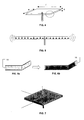
- Figure 4 shows a schematic layout of a prior-art patch-antenna.
- Figure 5 schematically shows the radiation of a patch-antenna.
- Figures 6a and 6b show the radiating slots for a two-plate structure and a multi-layer structure.
- Figure 7 shows a 3-dimensional view of a λ/2 coplanar multi-layer transformer patch-antenna.
- Figure 8 shows a possible configuration for the coplanar multi-layer transformer patch-antenna of the invention .
- Figure 9 again shows a coplanar multi-layer transformer antenna.
- As indicated before, figure 1 shows how impedance transforming could be achieved in the prior-art structures, by increasing the size of the active plate.
- Figure 2 shows diagrammatically how impedance transforming is carried out with the 1 to N coplanar multi-layer transformer of the present invention, which gives a 1:N2 impedance transformation ratio.
- This is also shown in figure 3: at the output the voltage Vout is divided by N, and the current Iout is multiplied by N, being the impedance multiplied by N2.
- This way, an impedance transformation is achieved between input and output, without increasing neither the horizontal nor the vertical dimensions, of the circuit.
- As indicated before, current electronic applications require devices of ever smaller dimensions with an ever increasing level of integration. Therefore, antennas has to be another element of the integrated device. Thus, the antenna has to be adapted to the miniaturisation requirements, both in the horizontal and vertical dimensions, of the present-day integrated circuits. This leads to horizontal dimensions being in the order of ten millimetres, while the vertical dimension is more constrained by the present-day integration technologies, which are below the millimetre,
- In the specific case of patch-based antennas, a diagrammatic layout of which is shown in figure 4, they have a very flat geometry.
- As a result of this, patch-based antennas have a very low impedance characteristic as transmission line:

where h is the thickness, εreff is the dielectric constant of the dielectric material, and we can be approached in this case by w (line width); and they have a very high impedance characteristic as a radiating element. For thickness h much smaller than λ, the radiating resistance will approximately be:
and having a width of w~0.25λ, that resistance gets to values around 500 Ω. - So, the smaller the radiating slot is, the higher the radiating impedance Z is. For 1 mm high slots, the impedance will be of the order of hundreds of ohms. The problem arising then is how to match the very low transmission line impedance (around 2-5 Ω) to the high radiation impedance (which can be as high as 300-500 Ω).
- Thus, the method of transforming impedance of the present invention is particularly appropriate for integrated antennas, as an impedance transforming effect of N2 can be obtained.
- Patch-antennas are formed by a radiating structure of parallel metallic planes or layers. This type of RF structures are fed by a transmission line (the coaxial wire in figures 4 and 5), and they basically behave as an electromagnetic resonant cavity with an electric and magnetic field distribution between the two conducting layers: the lower or ground plate and the upper or active layer. The radiation of this kind of structures can be interpreted as the one produced by the distribution of the electric and magnetic fields existing in the edges of the cavity (vertical walls of the cavity). The radiation of a patch-antenna is schematically shown in figure 5.
- While the impedance of the fields in the interior of the cavity (impedance as transmission line) is very low, the impedance of the slot expressed in circuit terms is very high. If this structure is made to radiate, being its height h very small, the difference between both impedances (in transmission and radiating modes) will be even higher, and the matching between them would be very difficult.
- Figures 6a and 6b show how in an RF structure (patch-antenna) which is 1 mm thick (that is, with 1 mm high radiating slots) N layers are introduced, these N layers being separated by a distance d which is in the order of a thousandth of the wavelength (d<<λ).
- In both the structures shown in figure 6a as in figure 6b the radiating
slots 10 are exactly the same, that is, they have the same dimensions (l x w x h). The radiatingslot 10 of the structure of figure 6b is fed by the N coplanar lines, the height of which is
- Figures 7-9 refer to a specific preferred embodiment of the present invention, which is a coplanar multi-layer transformer antenna.
- As shown in figure 9, the coplanar multi-layer impedance transformer comprises a set of N layered wave-guiding structures (conductor and dielectric structures) connecting a low impedance Zin point to a high radiating structure with impedance Zout (=N2Z0) through the N2 transforming relation.
- As indicated before, for a 1 mm thick patch-antenna, the characteristic impedance is increased if inside that 1 mm cavity several parallel metallic layers or sheets are introduced.
Claims (8)
- Method of transforming impedance in a structure, said structure comprising a coplanar line between a lower ground plate and an upper active plate, the method comprising:- providing N-1 substantially parallel conducting layers, being N≥2, inside the ground plate and the upper active plate of the structure, thereby having N coplanar lines,- injecting a current in a single first input layer, being said single first input layer the layer above the ground plate, and- using said N coplanar lines as output, whereby at the output the voltage is divided by N, and the current is multiplied by N, being the impedance multiplied by N2.
- Method of transforming impedance according to claim 1, wherein said structure is an antenna.
- Method of transforming impedance according to claim 2, wherein the method further comprises:- providing a radiating slot fed by the N coplanar lines, being the height of each one of the lines of h/N, where h is the height of the radiating slot.
- - A coplanar multi-layer impedance transformer in a structure, said structure comprising a coplanar line between a lower ground plate and an upper active plate, the coplanar multi-layer transformer comprising,- N-1 substantially parallel conducting layers, being N ≥2 inside the ground plate and the upper active plate of the structure, thereby having N coplanar lines,- injecting means for injecting current in a single first input layer , being said single first input layer the layer above the ground plate, and- output means constituted by said N coplanar lines, whereby at the output the voltage is divided by N, and the current is multiplied by N, being the impedance multiplied by N2.
- Coplanar multi-layer impedance transformer according to claim 4, wherein said structure is an antenna.
- Coplanar multi-layer impedance transformer according to claim 5, wherein said antenna further comprises:- a radiating slot fed by the N coplanar lines, being the height of each one of the lines of h/N, where h is the height of the radiating slot.
- Coplanar multi-layer impedance transformer according to claim 4, wherein said structure is a transmission line.
- Coplanar multi-layer impedance transformer according to claim 4, wherein said structure is a filter.
Priority Applications (3)
| Application Number | Priority Date | Filing Date | Title |
|---|---|---|---|
| EP05078048A EP1804331A1 (en) | 2005-12-30 | 2005-12-30 | Method of transforming impedance and coplanar multi-layer impedance transformer |
| JP2006349033A JP4301290B2 (en) | 2005-12-30 | 2006-12-26 | Impedance conversion method and coplanar multilayer impedance converter |
| US11/647,514 US20070194861A1 (en) | 2005-12-30 | 2006-12-28 | Method of transforming impedance and coplanar multi-layer impedance transformer |
Applications Claiming Priority (1)
| Application Number | Priority Date | Filing Date | Title |
|---|---|---|---|
| EP05078048A EP1804331A1 (en) | 2005-12-30 | 2005-12-30 | Method of transforming impedance and coplanar multi-layer impedance transformer |
Publications (1)
| Publication Number | Publication Date |
|---|---|
| EP1804331A1 true EP1804331A1 (en) | 2007-07-04 |
Family
ID=36282725
Family Applications (1)
| Application Number | Title | Priority Date | Filing Date |
|---|---|---|---|
| EP05078048A Withdrawn EP1804331A1 (en) | 2005-12-30 | 2005-12-30 | Method of transforming impedance and coplanar multi-layer impedance transformer |
Country Status (3)
| Country | Link |
|---|---|
| US (1) | US20070194861A1 (en) |
| EP (1) | EP1804331A1 (en) |
| JP (1) | JP4301290B2 (en) |
Citations (2)
| Publication number | Priority date | Publication date | Assignee | Title |
|---|---|---|---|---|
| WO1998054781A1 (en) * | 1996-05-31 | 1998-12-03 | Get Technology, Inc. | Guided energy transformer |
| EP1130676A2 (en) * | 2000-02-29 | 2001-09-05 | Lucent Technologies Inc. | Patch antenna with embedded impedance transformer and methods for making same |
-
2005
- 2005-12-30 EP EP05078048A patent/EP1804331A1/en not_active Withdrawn
-
2006
- 2006-12-26 JP JP2006349033A patent/JP4301290B2/en not_active Expired - Fee Related
- 2006-12-28 US US11/647,514 patent/US20070194861A1/en not_active Abandoned
Patent Citations (2)
| Publication number | Priority date | Publication date | Assignee | Title |
|---|---|---|---|---|
| WO1998054781A1 (en) * | 1996-05-31 | 1998-12-03 | Get Technology, Inc. | Guided energy transformer |
| EP1130676A2 (en) * | 2000-02-29 | 2001-09-05 | Lucent Technologies Inc. | Patch antenna with embedded impedance transformer and methods for making same |
Non-Patent Citations (3)
| Title |
|---|
| GRANHOLM J ET AL: "Probe-fed stacked microstrip patch antenna for high-resolution polarimetric C-band SAR", MICROWAVE CONFERENCE, 2000 ASIA-PACIFIC SYDNEY, NSW, AUSTRALIA 3-6 DEC. 2000, PISCATAWAY, NJ, USA,IEEE, US, 3 December 2000 (2000-12-03), pages 1377 - 1380, XP010545158, ISBN: 0-7803-6435-X * |
| SACHSE K ET AL: "Novel, multilayer coupled-line structures and their circuit applications", 22 May 2000, MICROWAVES, RADAR AND WIRELESS COMMUNICATIONS. 2000. MIKON-2000. 13TH INTERNATIONAL CONFERENCE ON MAY 22-24, 2000, PISCATAWAY, NJ, USA,IEEE, PAGE(S) 131-155, ISBN: 83-906662-3-5, XP010537480 * |
| YAXUN LIU ET AL: "Gain improvement of an array of sequentially rotated circularly polarized microstrip antennas using stacked parasitic patches", 22 June 2003, IEEE ANTENNAS AND PROPAGATION SOCIETY INTERNATIONAL SYMPOSIUM. 2003 DIGEST. APS. COLUMBUS, OH, JUNE 22 - 27, 2003, NEW YORK, NY : IEEE, US, PAGE(S) 614-617, ISBN: 0-7803-7846-6, XP010649537 * |
Also Published As
| Publication number | Publication date |
|---|---|
| JP4301290B2 (en) | 2009-07-22 |
| JP2007184917A (en) | 2007-07-19 |
| US20070194861A1 (en) | 2007-08-23 |
Similar Documents
| Publication | Publication Date | Title |
|---|---|---|
| CN101814651B (en) | Antenna and printed circuit board using a waveguide structure | |
| US20210399427A1 (en) | Self-filtering wideband millimeter wave antenna | |
| JP4768749B2 (en) | An electronically scanned antenna for a transverse device array radiator. | |
| US10923831B2 (en) | Waveguide-fed planar antenna array with enhanced circular polarization | |
| JP4142713B2 (en) | High efficiency cross slot microstrip antenna | |
| CN1150660C (en) | Multiband Printed Monopole Antenna | |
| CN113454848A (en) | Antenna array based on one or more metamaterial structures | |
| US20080218417A1 (en) | Probe fed patch antenna | |
| KR20140051785A (en) | Compact slot antenna | |
| JP3996879B2 (en) | Coupling structure of dielectric waveguide and microstrip line, and filter substrate having this coupling structure | |
| KR102444699B1 (en) | waveguide slot antenna | |
| CN110783704A (en) | Dual-via-hole probe feed integrated substrate gap waveguide circularly polarized antenna | |
| CN110212273A (en) | Two-frequency duplex device based on substrate integration wave-guide | |
| Maulidini et al. | Band-pass filter microstrip at 3 GHz frequency using square open-loop resonator for S-band radar applications | |
| WO2023113940A1 (en) | Self supporting stripline structure | |
| US20150123861A1 (en) | Method For Creating A Slot-Line On a Multilayer Substrate and Multilayer Printed Circuit Comprising at Least One Slot-Line Realized According to Said Method and Used as an Isolating Slot or Antenna | |
| US12003026B2 (en) | Antenna device and vehicle comprising an antenna device | |
| Deng et al. | Slow-wave substrate integrated groove gap waveguide | |
| Rahimi et al. | Development of a slow-wave artificial dielectric substrate-based microstrip line in X band | |
| EP1804331A1 (en) | Method of transforming impedance and coplanar multi-layer impedance transformer | |
| JP7077137B2 (en) | Transmission lines and connectors | |
| Metlevskis et al. | Computer models of meander slow-wave system with additional shields | |
| KR20150112891A (en) | Filtering circuit with slot line resonators | |
| US11251513B2 (en) | Waveguide to laminated circuit board transition comprising a lateral coupling through a sidewall of the waveguide | |
| US20180108970A1 (en) | Switchable radiators and operating method for the same |
Legal Events
| Date | Code | Title | Description |
|---|---|---|---|
| PUAI | Public reference made under article 153(3) epc to a published international application that has entered the european phase |
Free format text: ORIGINAL CODE: 0009012 |
|
| 17P | Request for examination filed |
Effective date: 20070123 |
|
| AK | Designated contracting states |
Kind code of ref document: A1 Designated state(s): AT BE BG CH CY CZ DE DK EE ES FI FR GB GR HU IE IS IT LI LT LU LV MC NL PL PT RO SE SI SK TR |
|
| AX | Request for extension of the european patent |
Extension state: AL BA HR MK YU |
|
| AKX | Designation fees paid |
Designated state(s): DE FI GB |
|
| STAA | Information on the status of an ep patent application or granted ep patent |
Free format text: STATUS: THE APPLICATION HAS BEEN WITHDRAWN |
|
| 18W | Application withdrawn |
Effective date: 20090728 |