EP1804249A1 - Address decoder, storage device, processor device, and address decoding method for the storage device - Google Patents
Address decoder, storage device, processor device, and address decoding method for the storage device Download PDFInfo
- Publication number
- EP1804249A1 EP1804249A1 EP06251653A EP06251653A EP1804249A1 EP 1804249 A1 EP1804249 A1 EP 1804249A1 EP 06251653 A EP06251653 A EP 06251653A EP 06251653 A EP06251653 A EP 06251653A EP 1804249 A1 EP1804249 A1 EP 1804249A1
- Authority
- EP
- European Patent Office
- Prior art keywords
- decode
- circuit
- units
- memory cells
- address
- Prior art date
- Legal status (The legal status is an assumption and is not a legal conclusion. Google has not performed a legal analysis and makes no representation as to the accuracy of the status listed.)
- Granted
Links
Images




Classifications
-
- G—PHYSICS
- G11—INFORMATION STORAGE
- G11C—STATIC STORES
- G11C11/00—Digital stores characterised by the use of particular electric or magnetic storage elements; Storage elements therefor
- G11C11/21—Digital stores characterised by the use of particular electric or magnetic storage elements; Storage elements therefor using electric elements
- G11C11/34—Digital stores characterised by the use of particular electric or magnetic storage elements; Storage elements therefor using electric elements using semiconductor devices
- G11C11/40—Digital stores characterised by the use of particular electric or magnetic storage elements; Storage elements therefor using electric elements using semiconductor devices using transistors
- G11C11/401—Digital stores characterised by the use of particular electric or magnetic storage elements; Storage elements therefor using electric elements using semiconductor devices using transistors forming cells needing refreshing or charge regeneration, i.e. dynamic cells
- G11C11/4063—Auxiliary circuits, e.g. for addressing, decoding, driving, writing, sensing or timing
- G11C11/407—Auxiliary circuits, e.g. for addressing, decoding, driving, writing, sensing or timing for memory cells of the field-effect type
-
- G—PHYSICS
- G11—INFORMATION STORAGE
- G11C—STATIC STORES
- G11C8/00—Arrangements for selecting an address in a digital store
- G11C8/10—Decoders
-
- G—PHYSICS
- G06—COMPUTING OR CALCULATING; COUNTING
- G06F—ELECTRIC DIGITAL DATA PROCESSING
- G06F12/00—Accessing, addressing or allocating within memory systems or architectures
- G06F12/02—Addressing or allocation; Relocation
-
- G—PHYSICS
- G06—COMPUTING OR CALCULATING; COUNTING
- G06F—ELECTRIC DIGITAL DATA PROCESSING
- G06F13/00—Interconnection of, or transfer of information or other signals between, memories, input/output devices or central processing units
-
- G—PHYSICS
- G11—INFORMATION STORAGE
- G11C—STATIC STORES
- G11C11/00—Digital stores characterised by the use of particular electric or magnetic storage elements; Storage elements therefor
Definitions
- the present invention relates to the technology of decode processing for address signals in SRAMs (Static RAM) provided for processor devices such as CPUs (Central Processing Units).
- SRAMs Static RAM
- processor devices such as CPUs (Central Processing Units).
- SRAM Static RAM circuits, which are used in registers of CPUs (Central Processing Units) and cache memories, are provided with multiple memory cells for storing data therein, which memory cells are arranged in an array form.
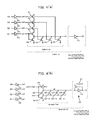
- FIG. 7 is a view showing a decode circuit and a memory cell of an SRAM.
- FIG. 8 is a diagram showing the decode circuit of FIG. 7 as a combination of two parts thereof: a predecoder; and a main decoder. In this instance, in the examples of FIG. 7 and FIG. 8, only one of the multiple memory cells is illustrated.
- FIG. 9 is a view showing a decode circuit and memory cells of a previous SRAM.
- This example is realized by a NAND circuit which is formed by a dynamic circuit ⁇ a circuit in which precharging is performed by a single pMOS circuit [p channel MOS (Metal Oxide Semiconductor)] and a logic function is configured with multiple nMOS (n channel MOS) circuits, when no clock is input ⁇ .
- a NAND circuit which is formed by a dynamic circuit ⁇ a circuit in which precharging is performed by a single pMOS circuit [p channel MOS (Metal Oxide Semiconductor)] and a logic function is configured with multiple nMOS (n channel MOS) circuits, when no clock is input ⁇ .
- an SRAM 50 includes multiple memory cells 51 arranged in an array form (cell array 53; see FIG. 9) and a decode circuit (decoder) 52. These decode circuit 52 and memory cells 51 are connected to each other through a word line (select signal line) 54.
- the decode circuit 52 decodes (address decoding) address signals, and is provided one for each memory cell 51.
- the decode circuit 52 decodes address signals received from outside the SRAM 50 and activates a word line 54 corresponding to the decode result, whereby read/write processing to the corresponding memory cell 51 is carried out.
- reference character AD[*] (* is an integer of 0 through i-1; i is a natural number expressing the bit width of the address) denotes an input address, and the address signals corresponding to the input address are input.
- reference character PC designates a precharge signal
- reference character EN designates an enable signal.
- FIG. 9 shows a construction of a decode circuit 52 which activates a memory cell 51-2, out of the memory cells 51-1 through 51-5 forming the cell array 53.
- the decode circuit 52 is formed by two parts, a predecode circuit (predecoder) 521 and a main decode circuit (main decoder) 522, with consideration paid to the circuit size, wiring convenience, and delay.
- the predecoder 521 is equipped with decode units 55a formed by multiple combination logic circuits
- the main decoder 522 is equipped with decode units 55b also formed by multiple combination logic circuits.
- decode units 55a formed by multiple combination logic circuits
- main decoder 522 is equipped with decode units 55b also formed by multiple combination logic circuits.
- FIG. 9 for convenience of illustration, only one decode unit 55b is shown.
- predecoder 521 address signals are input to each of the decode units 55a and subjected to predecode processing. After that, the output signals from the decode units 55a are input to the decode units 55b of the main decoder 522 and subjected to main decode processing.
- these predecoder 521 and main decoder 522 are realized by NAND logic in the decode process in which the decode construction is divided into a predecoder and a main decoder, from the view point of good compatibility due to a construction using negative logic.
- the following techniques for increasing the speed of address decoding in an SRAM 50 are also used: dynamizing of a static circuit; increasing driving power, thereby improving delay; reducing the number of stages of n channel transistor tree connected in series and adjustment of the size thereof.
- dynamizing of the static circuit is a technique in which a circuit is formed using only nMOS transistors, without using pMOS transistors. As a result, since the load of pMOS transistors can be reduced, the circuits are improved in speed.
- Patent Document 1 Japanese Patent Application Laid-open No. 2002-63792
- NOR logic can be used to realize decode processing. Further, this NOR logic can be dynamized (dynamic NOR circuit). By realizing the decode circuit 52 using a dynamic NOR circuit, the decode time is made to be fixed (for example, two steps) regardless of the number of addresses, so that address decoding can be improved in speed.
- a decode circuit when a decode circuit is realized by a dynamic NOR circuit, (1) its output maintains the state of "H” when it matches an input address, and (2) its output is changed from the state of "H” to "L” when it does not match an input address. That is, except for the time during which decoding is being performed, all the word lines 54 are activated, thereby increasing power consumption, so that it is not preferable from the standpoint of an operation.
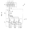
- FIG. 10 is a view showing a decode circuit and memory cells of a previous SRAM.
- the decode circuit 52 is realized by a dynamic NOR circuit, and an AND circuit is provided for an output of the main decoder 522.
- the main decoder 522 is provided for an output of the main decoder 522.
- only one decode unit 55b is illustrated for the convenience of illustration.
- the example of FIG. 10 is provided with an AND circuit 56 at the output end of the decode units 55b of the main decoder 522.
- an output of the main decoder 22 and an enable clock (EN_B) are input, and an output of the main decoder 22 is pulsed with this enable clock.
- an address decoder connected to memory cells for selectively activating the memory cells according to input address signals
- the address decoder comprising: a plurality of decode units each formed by a combinational logic circuit; at least one inverting circuit which inverts an output of a corresponding one of the decode units; and an AND circuit which performs a logical AND operation between an output signal of the decode unit, which has been inverted by the inverting circuit, and another one of the plurality of decode units.
- the address decoder further comprises: a plurality of predecode units which decode the input address signals, wherein the decode unit is connected to the plurality of predecode units, and receives outputs of the plurality of predecode units, and performs further decoding thereof.
- a storage device comprising: a plurality of memory cells for storing information therein; and an address decoder which is connected to the memory cells and selectively activates the memory cells according to input address signals, the address decoder including: a plurality of decode units; an-inverting circuit which inverts an output of one of the decode units; and an AND circuit which performs a logical AND operation between an output signal of the decode unit, which has been inverted by the inverting circuit, and another one of the plurality of decode units, and outputs the operation result as a select signal for activating the memory cells.
- the storage device further comprises: a plurality of predecode units which decode the input address signals, wherein the decode unit is connected to the plurality of predecode units, and receives outputs of the plurality of predecode units, and performs further decoding thereof.
- a processor device comprising a storage device, the storage device including: a plurality of memory cells for storing information therein; and an address decoder which is connected to the memory cells and selectively activates a memory cell according to input address signals, the address decoder including: a plurality of decode units each formed by a combinational logic circuit; inverting circuits which invert respective outputs of at least some of the decode units; at least one AND circuit which performs a logical AND operation between an output signal of one of the decode units, which has been inverted by the inverting circuit, and the non-inverted output signal of another one of the plurality of decode units, and outputs the operation result as a select signal for activating the memory cells.
- the address decoder includes: a plurality of predecode units which decode the input address signals, wherein the decode unit is connected to the plurality of predecode units, and receives outputs of the plurality of predecode units, and performs further decoding thereof.
- Another aspect of the present invention provides an address decoding method for a storage device which selectively activates a memory cell according to input address signals, the method comprising: decoding the input address signals by means of a combination logic circuit; inverting at least partly the decode results obtained by the decoding step; and performing a logical AND operation between each of one or more decoding results, which have been inverted by the inverting step, and a non-inverted decoding result obtained by the decoding step, respectively; and outputting the operation result as a select signal for activating said memory cells.
- the decoding step includes: a plurality of predecodings for decoding the input address signals; and a main decoding step for receiving the decoding result obtained by the plurality of predecodings and performing further decoding thereof.
- the predecodings occur in parallel.
- FIG. 1 is a diagram schematically showing a construction of an SRAM according to one preferred embodiment of the present invention
- FIG. 2 is a diagram schematically showing a construction of a processor including an SRAM according to the present embodiment
- FIG. 3 is a view for describing processing performed by a processor of FIG. 2.
- an SRAM Static Random Access Memory; a semiconductor storage circuit which does not require a storage operation (refresh)] according to one preferred embodiment of the present invention is used as a memory circuit, such as an L1-Cache and an L2-Cache, which is provided within the same chip as that of the processor (processor device) 100 such as CPU (Central Processing Unit).
- processor processor device
- FIG. 2 is a cutaway view of the processor 100.
- the L1 cache 102a functions as a data cache, and is used for performing processing such as data loading and data storing, etc, at the time of process execution by the processor 100.
- L1 cache 102b functions as an instruction cache, and performs processing such as fetch (Instruction Fetch).
- the SRAM 20 of the present embodiment includes an address decoder 10 and a memory cell array 30.
- the memory cell array 30 includes multiple (three in FIG. 1) memory cells 17-1, 17-2, and 17-3, arranged in an array form. Each of the memory cells 17-1, 17-2, and 17-3 stores data therein, thereby retaining various kinds of information.
- reference characters 17-1, 17-2, and 17-3 are used.
- reference character 17 is used.
- An address decoder 10 which decodes (address decode; decode, analysis) address signals received from the outside of the SRAM 20, is provided one for each of the multiple memory cells 17, and is connected to the corresponding memory cells 17 through word lines (select signal line) 40.
- reference character AD[*] (where * is an integer of 0 through i-1 ; i is a natural number which represents an address bit width) expresses an input address, and address signals corresponding to this input address are input. Further, reference character PC designates a precharge signal; reference character EN designates an enable signal.
- the address decoder 10 has a predecoder (predecoder circuit) 11 and a main decoder (main decode circuit) 12.
- the predecoder 11 includes multiple (three in FIG. 1) predecode units (decode units) 15-1, 15-2, and 15-3;
- the main decoder 12 includes multiple (three in FIG. 1) main decode units (decode units) 13-1, 13-2, and 13-3.
- Predecoder 11 and main decoder 12 evaluate whether or not input signals match address data which has been set beforehand, thereby carrying out decode processing.
- reference characters 15-1, 15-2, and 15-3 are used.
- reference character 15 is used.
- reference characters 13-1, 13-2, and 13-3 are used.
- reference character 13 is used.
- the predecode units 15-1, 15-2, and 15-3, and the main decode units 13-1, 13-2, and 13-3 are each realized by dynamic NOR circuits (NOR circuits formed by dynamic circuits).
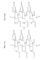
- FIG. 4(a) and FIG. 4(b) are views each for describing a dynamic NOR circuit used in an SRAM 20 according to the present embodiment.
- FIG. 4(a) shows an example of a static NOR circuit
- FIG. 4(b) shows an example of a dynamic NOR circuit.
- the static NOR (static-nor) circuit includes inverters (NOT circuits) 63 and 64, pMOS transistors 61, and nMOS transistors 62.
- the number [four in FIG. 4(a)] of inverters 64 is equal to the number of input signals.
- the inverters 64 invert address signals A1 through A4 input from the outside, and generate signals xa1, xa2, xa3, and xa4.
- the number [four in FIG. 4(a)] of pMOS transistors 61 is equal to the number of input signals, and these pMOS transistors 61 are arranged in series.
- the inverted signals xa1 through xa4 of input signals A1 through A4 are input one to each of the pMOS transistors 61.
- the number [four in FIG. 4(a)] of nMOS transistors 62 is equal to the number of input signals, and are arranged in parallel downstream of the pMOS transistors 61.
- the dynamic NOR (dynamic-nor) circuit used in the address decoder 10 of the present SRAM 20 includes inverters (NOT circuits) 64, nMOS transistor 62-1, 62-2, 62-3, 62-4, and 62-5, and a precharged transistor 65.
- the number [four in FIG. 4(b)] of inverters 64 is equal to the number of input signals.
- the inverters 64 invert address signals A1 through A4 input from the outside, and generate signals xa1, xa2, xa3, and xa4.
- nMOS transistor 62-1, 62-2, 62-3, and 62-4 are arranged in parallel, and receive inverted signals xa1 through xa4 of input signals A1 through A4 inverted by the inverter 64. Further, the nMOS transistor 62-5, together with the precharge transistor (PC) 65, is arranged in series with the nMOS transistor 62-1.
- the precharge transistor 65 sets a dynamic node (nd), which is to be precharged, to "High” beforehand, and discharges the dynamic node (nd) to "Low” when more than one of the inputs terminals turns to be “High”.
- the inverting circuit 66 includes an inverter 63 and a keeper transistor (Keeper) 67 which forcibly maintains a high level once the output becomes "Low".
- the dynamic circuit when the precharge transistor 65 is in an off state and all the input terminal levels are low, the dynamic node (nd) falls in an unstable state called a floating state in which the dynamic node is connected neither to Vdd nor to Vss. At a state of normal use, such a state will cause an erroneous operation, and thus, the keeper transistor 67 prevents level lowering due to leakage.
- the dynamic NOR circuit is formed by nMOS transistors, the loads of pMOS transistors can be reduced, whereby the circuit is simplified and improved in speed.
- the main decoder 12 has AND circuits-14-1, 14-2, and 14-3, and inverters (NOT circuits) 16-1, 16-2, and 16-3, provided downstream of the main decoder units 13-1, 13-2, and 13-3.
- reference characters 14-1 through 14-3 are used.
- reference character 14 is used.
- reference characters 16-1 through 16-3 are used.
- reference character 16 is used.
- the inverter 16 inverts an output signal from the main decode unit 13. This inverter 16 receives an output signal from the main decode units 13. Further, the output signal from the main decode unit 13, which has been inverted by the inverter 16, is input to the AND circuit 14.
- the AND circuit 14 obtains a logical AND between an output signal of one decode unit and an output signal of another decoded unit 13, which has been inverted by the inverter 16, and outputs the result as a select signal for activating a memory cell 17.
- This AND circuit 14 receives an output signal of a main decode unit 13, which is provided upstream of the AND circuit 14, and an output signal of another main decode unit 13 adjacent to the above main decode unit 13, which output signal is an inverted signal inverted by the inverter 16.
- the AND circuit 14-1 receives an output signal of the main decode unit 13-1 and an output signal (inverted signal) which is output from the main decode unit 13-2 and is then inverted by the inverter 16-1.
- the AND circuit 14-2 receives an output signal of the main decode unit 13-2 and an output signal (inverted signal) which is output from the main decoded unit 13-3 and is then inverted by the inverter 16-2.
- FIG. 5 (a) and FIG. 5 (b) are diagrams for describing a construction of a main decoder 12 of an SRAM 20 according to the present embodiment.
- FIG. 5 (a) shows an example of an initial state before decode processing is performed;
- FIG. 5(b) shows a state after decode processing is performed.
- the main decode unit 13-1 and the main decoded unit 13-3 outputs "Low (L)", and the main decode unit 13-2 outputs "High (H)".
- the word line 40-2 is selected, and the state is changed from “L” to "H", and the state of the other lines 40-1 and 40-2 maintain "L".
- the output potential of a decoder which does not match an input address is changed from “H” to "L". If this output result of the unselected circuit is regarded as a pulse signal changing from "High (H) “ to “Low (L) ", this signal after having being inverted by the inverter 16 can be treated as "an enable clock which has been subjected to timing adjustment with an output (main decode unit output) from the main decode units 13".
- the main decode units 13 are capable of realizing an operation such that (1) the state of the selected word line 40 is changed from “L” to "H” and (2) the state of the other word lines 40 maintains "L".
- a main decode unit 13 is capable of using a signal which is output from another main decode unit 13 adjacent thereto and is then inverted by the inverter 16 as an enable clock.
- This arrangement eliminates the necessity of preparing a circuit for generating an enable clock, thereby simplifying the circuit configuration and reducing power consumption. In addition, it becomes unnecessary to perform timing adjustment among main decoder units 13 in the main decoder 12.
- FIG. 6 is a diagram showing a concrete example of a construction of an SRAM 20 according to one preferred embodiment of the present invention. Referring to this FIG. 6, a description will be made hereinbelow of processing performed by the address decoder 10 of the present SRAM 20.
- FIG. 6 shows an address decoder 10 for the memory cell 17-2 in the memory cell array 30.
- 6-bit address signals (AD[0] through AD[5]) are input.
- the predecoder 11 includes predecode units 15-1 through 15-6;
- the main decoder 12 includes main decode units 13-1 through 13-4.
- a keeper transistor 67 (see FIG. 4) of each predecode unit (15) is omitted.
- the node 152 when an input address signal matches address data having been set beforehand, the node 152 outputs "L", otherwise, the node 151 is discharged and outputs "H" to the node 152.
- the main decode unit 13 includes a NOR unit 131 and a NAND unit 132.
- the main decode unit 13 receives the result of the predecode unit 15 and performs decode processing thereof.
- the node 133 maintains "H”. If the result does not match the address data the node 133 is discharged to "L".
- the decode result is output to the NAND unit 132 at the later stage, and is also output to the NAND unit 132 of the adjacent main decode unit 13 via the inverter 16 as an enable signal (see arrow a).
- the NAND unit 132 receives the result of the NOR unit 131 and an enable signal from another main decode unit 13. Only when a condition is met, the NAND unit 132 makes the result into a pulse ("L to H"), or otherwise, outputs "L" to the word line 40. With this arrangement, it is possible to perform read/write operations to an arbitrary cell.
- each main decode unit 13 when the number of predecoded signals which are received by each main decode unit 13 is n , ( n -1)-number of input signals make a group, and sending/receiving of an enable signal is performed within this group.
- signal A and signal B are arranged in a common group, thereby making it possible to transceive an enable signal.
- the number of signals in which variation should be considered is reduced to two, and thus, timing ensured between these two signals can suppress erroneous operations, so that effort required in circuit design is reduced.
- the processing speed of the decoder is increased.
- the necessity of an additional circuit for generating an enable signal for the main decode unit 13 is eliminated, whereby the circuit construction is simplified.
- an enable signal for the main decoder 12 is generated within the main decoder 12, so that timing adjustment with each input signal is not necessary. Hence, effort required in circuit design is reduced.
- the number of bits input to the address decoder 10 should not be limited to six, and two through five bits or more than seven bits can be applied.
- predecode unit 15 and the main decode unit 13 should by no means be limited to those of the above-described embodiment, and various changes or modifications may be made.
- the present invention can be summarized as follows.
- a processor device comprising a semiconductor memory, the semiconductor memory including:
- the address decoder comprises:
- a semiconductor storage circuit comprising:
- the address decoder comprises:
- an address decoder provided corresponding to a plurality of memory cells, for selectively activating one of the memory cells according to the address signals input therein, the address decoder comprising:
- the address decoder further comprises:
- the application of the present invention should by no means be limited to address signal decoding, and the present application can be applied to decoding processes of various types of information.
Landscapes
- Engineering & Computer Science (AREA)
- Theoretical Computer Science (AREA)
- Microelectronics & Electronic Packaging (AREA)
- Computer Hardware Design (AREA)
- Physics & Mathematics (AREA)
- General Engineering & Computer Science (AREA)
- General Physics & Mathematics (AREA)
- Static Random-Access Memory (AREA)
- Compression, Expansion, Code Conversion, And Decoders (AREA)
Abstract
Description
- The present invention relates to the technology of decode processing for address signals in SRAMs (Static RAM) provided for processor devices such as CPUs (Central Processing Units).
- SRAM (Static RAM) circuits, which are used in registers of CPUs (Central Processing Units) and cache memories, are provided with multiple memory cells for storing data therein, which memory cells are arranged in an array form.
- FIG. 7 is a view showing a decode circuit and a memory cell of an SRAM. FIG. 8 is a diagram showing the decode circuit of FIG. 7 as a combination of two parts thereof: a predecoder; and a main decoder. In this instance, in the examples of FIG. 7 and FIG. 8, only one of the multiple memory cells is illustrated. FIG. 9 is a view showing a decode circuit and memory cells of a previous SRAM. This example is realized by a NAND circuit which is formed by a dynamic circuit {a circuit in which precharging is performed by a single pMOS circuit [p channel MOS (Metal Oxide Semiconductor)] and a logic function is configured with multiple nMOS (n channel MOS) circuits, when no clock is input}.
- Hereinafter, to configure a circuit using a dynamic circuit will sometimes be referred to as "to dynamize a circuit".
- As shown in FIG. 7, an
SRAM 50 includesmultiple memory cells 51 arranged in an array form (cell array 53; see FIG. 9) and a decode circuit (decoder) 52. Thesedecode circuit 52 andmemory cells 51 are connected to each other through a word line (select signal line) 54. - The
decode circuit 52 decodes (address decoding) address signals, and is provided one for eachmemory cell 51. Thedecode circuit 52 decodes address signals received from outside theSRAM 50 and activates aword line 54 corresponding to the decode result, whereby read/write processing to thecorresponding memory cell 51 is carried out. - Hereafter, reference character AD[*] (* is an integer of 0 through i-1; i is a natural number expressing the bit width of the address) denotes an input address, and the address signals corresponding to the input address are input. Further, reference character PC designates a precharge signal, and reference character EN designates an enable signal.
- The example of FIG. 9 shows a construction of a
decode circuit 52 which activates a memory cell 51-2, out of the memory cells 51-1 through 51-5 forming thecell array 53. - Generally speaking, as shown in FIG. 8 and FIG. 9, the
decode circuit 52 is formed by two parts, a predecode circuit (predecoder) 521 and a main decode circuit (main decoder) 522, with consideration paid to the circuit size, wiring convenience, and delay. Thepredecoder 521 is equipped withdecode units 55a formed by multiple combination logic circuits, and themain decoder 522 is equipped withdecode units 55b also formed by multiple combination logic circuits. In FIG. 9, for convenience of illustration, only onedecode unit 55b is shown. - In the
predecoder 521, address signals are input to each of thedecode units 55a and subjected to predecode processing. After that, the output signals from thedecode units 55a are input to thedecode units 55b of themain decoder 522 and subjected to main decode processing. - Further, in the
previous SRAM 50, thesepredecoder 521 andmain decoder 522 are realized by NAND logic in the decode process in which the decode construction is divided into a predecoder and a main decoder, from the view point of good compatibility due to a construction using negative logic. - Enhanced speed in address decode processing is demanded in the art of
SRAM 50. For example, the followingpatent document 1 discloses an art in which address signals are propagated to a decoder before a control signal which gives instructions about an operation of memory cells is activated. As a result, a decoder is activated after the activation of the control signal, thereby outputting decode signals, so that the speed of access is increased and erroneous operations are prevented. - The following techniques for increasing the speed of address decoding in an
SRAM 50 are also used: dynamizing of a static circuit; increasing driving power, thereby improving delay; reducing the number of stages of n channel transistor tree connected in series and adjustment of the size thereof. - Here, as shown in FIG. 9, dynamizing of the static circuit is a technique in which a circuit is formed using only nMOS transistors, without using pMOS transistors. As a result, since the load of pMOS transistors can be reduced, the circuits are improved in speed.
[Patent Document 1]Japanese Patent Application Laid-open No. 2002-63792 - However, in such previous SRAMs, if the drive power (drive ability) of transistors is simply increased for the purpose of increasing the speed of address decoding, the size of transistors is increased, so that the layout area is enlarged and the input capacity of a decoder and power consumption are increased.
- Further, in cases where decode processing is realized by NAND logic, assuming that the number of address inputs is N, and that the number of predecoder inputs is i, the number of inputs to the main decoder is j = CELL (N/i) (CELL(x) ... a ceiling function for x). Even though dynamizing is performed, the gate pass time in parallel with the (i + j) step (roughly estimated) is necessary for the address decode processing.
- Here, in place of NAND logic, NOR logic can be used to realize decode processing. Further, this NOR logic can be dynamized (dynamic NOR circuit). By realizing the
decode circuit 52 using a dynamic NOR circuit, the decode time is made to be fixed (for example, two steps) regardless of the number of addresses, so that address decoding can be improved in speed. - However, when a decode circuit is realized by a dynamic NOR circuit, (1) its output maintains the state of "H" when it matches an input address, and (2) its output is changed from the state of "H" to "L" when it does not match an input address. That is, except for the time during which decoding is being performed, all the
word lines 54 are activated, thereby increasing power consumption, so that it is not preferable from the standpoint of an operation. - FIG. 10 is a view showing a decode circuit and memory cells of a previous SRAM. In this example, the
decode circuit 52 is realized by a dynamic NOR circuit, and an AND circuit is provided for an output of themain decoder 522. In the example of FIG. 10, also, only onedecode unit 55b is illustrated for the convenience of illustration. - For the purpose of decreasing power consumption, the example of FIG. 10 is provided with an
AND circuit 56 at the output end of thedecode units 55b of themain decoder 522. To this ANDcircuit 56, an output of the main decoder 22 and an enable clock (EN_B) are input, and an output of the main decoder 22 is pulsed with this enable clock. - However, as shown in FIG. 10, since the
previous SRAM 50 has anAND circuit 56 arranged at the output end of themain decoder 522, a circuit for generating an enable clock needs to be provided. In addition, in themain decoder 522, timing adjustment required to be performed among the outputs of thedecode units 55b makes the circuit construction complicated, and timing adjustment is troublesome. - Further, operation must be guaranteed against manufacturing variations caused by miniaturization and high-density packaging of semiconductor devices at the time of manufacturing of
SRAMs 50. Hence, a sufficient set-up time (the minimum margin time from when a signal is defined to when a clock is changed) needs to be ensured. - It is thus desirable (i) to simplify a circuit construction, (ii) to improve the speed of processing and (iii) to reduce power consumption.
- According to one aspect of the present invention, there is provided an address decoder connected to memory cells for selectively activating the memory cells according to input address signals, the address decoder comprising: a plurality of decode units each formed by a combinational logic circuit; at least one inverting circuit which inverts an output of a corresponding one of the decode units; and an AND circuit which performs a logical AND operation between an output signal of the decode unit, which has been inverted by the inverting circuit, and another one of the plurality of decode units.
- As a preferred feature, the address decoder further comprises: a plurality of predecode units which decode the input address signals, wherein the decode unit is connected to the plurality of predecode units, and receives outputs of the plurality of predecode units, and performs further decoding thereof.
- In another aspect, there is provided a storage device, comprising: a plurality of memory cells for storing information therein; and an address decoder which is connected to the memory cells and selectively activates the memory cells according to input address signals, the address decoder including: a plurality of decode units; an-inverting circuit which inverts an output of one of the decode units; and an AND circuit which performs a logical AND operation between an output signal of the decode unit, which has been inverted by the inverting circuit, and another one of the plurality of decode units, and outputs the operation result as a select signal for activating the memory cells.
- As a preferred feature, the storage device further comprises: a plurality of predecode units which decode the input address signals, wherein the decode unit is connected to the plurality of predecode units, and receives outputs of the plurality of predecode units, and performs further decoding thereof.
- In a further aspect, there is provided a processor device, comprising a storage device, the storage device including: a plurality of memory cells for storing information therein; and an address decoder which is connected to the memory cells and selectively activates a memory cell according to input address signals, the address decoder including: a plurality of decode units each formed by a combinational logic circuit; inverting circuits which invert respective outputs of at least some of the decode units; at least one AND circuit which performs a logical AND operation between an output signal of one of the decode units, which has been inverted by the inverting circuit, and the non-inverted output signal of another one of the plurality of decode units, and outputs the operation result as a select signal for activating the memory cells.
- As a preferred feature, the address decoder includes: a plurality of predecode units which decode the input address signals, wherein the decode unit is connected to the plurality of predecode units, and receives outputs of the plurality of predecode units, and performs further decoding thereof.
- Another aspect of the present invention provides an address decoding method for a storage device which selectively activates a memory cell according to input address signals, the method comprising: decoding the input address signals by means of a combination logic circuit; inverting at least partly the decode results obtained by the decoding step; and performing a logical AND operation between each of one or more decoding results, which have been inverted by the inverting step, and a non-inverted decoding result obtained by the decoding step, respectively; and outputting the operation result as a select signal for activating said memory cells.
- As a preferred feature, the decoding step includes: a plurality of predecodings for decoding the input address signals; and a main decoding step for receiving the decoding result obtained by the plurality of predecodings and performing further decoding thereof. The predecodings occur in parallel.
- The present invention enables at least one of the following advantageous results:
- (1) the circuit construction is simplified, so that the circuit area is decreased and the processing speed is improved;
- (2) power consumption is reduced;
- (3) effort in circuit design is reduced;
- (4) timing self-correction effects can be expected with respect to manufacturing variations at the time of LSI manufacturing.
- Further features of the present invention will be apparent from the following detailed description when read in conjunction with the accompanying drawings, in which:
- FIG. 1 is a diagram schematically showing a construction of an SRAM according to one preferred embodiment of the present invention;
- FIG. 2 is a diagram schematically showing a construction of a processor including an SRAM according to the present embodiment;
- FIG. 3 is a view for describing processing performed by a processor of FIG. 2;
- FIG. 4 (a) and FIG. 4 (b) are views each for describing a NOR circuit used in an SRAM according to the present embodiment;
- FIG. 5 (a) and FIG. 5 (b) are views each for describing a construction of a main decoder of an SRAM according to the present embodiment;
- FIG. 6 is a view showing a concrete example of a construction of an SRAM according to the present embodiment;
- FIG. 7 is a view showing a decode circuit and a memory cell of an SRAM;
- FIG. 8 is a view showing a predecoder and a main decoder of a decode circuit of the SRAM of FIG. 7;
- FIG. 9 is a view showing a decode circuit and memory cells of a previous SRAM; and
- FIG. 10 is a view showing a decode circuit and memory cells of a previous SRAM.
- One preferred embodiment of the present invention will now be described with reference to the relevant accompanying drawings.
- FIG. 1 is a diagram schematically showing a construction of an SRAM according to one preferred embodiment of the present invention; FIG. 2 is a diagram schematically showing a construction of a processor including an SRAM according to the present embodiment; FIG. 3 is a view for describing processing performed by a processor of FIG. 2.
- As shown in FIG. 2, an SRAM [Static Random Access Memory; a semiconductor storage circuit which does not require a storage operation (refresh)] according to one preferred embodiment of the present invention is used as a memory circuit, such as an L1-Cache and an L2-Cache, which is provided within the same chip as that of the processor (processor device) 100 such as CPU (Central Processing Unit). In this instance, FIG. 2 is a cutaway view of the
processor 100. - As shown in FIG. 3, in the
processor 100, theL1 cache 102a functions as a data cache, and is used for performing processing such as data loading and data storing, etc, at the time of process execution by theprocessor 100. Further,L1 cache 102b functions as an instruction cache, and performs processing such as fetch (Instruction Fetch). - As shown in FIG. 1, the
SRAM 20 of the present embodiment includes anaddress decoder 10 and amemory cell array 30. - The
memory cell array 30 includes multiple (three in FIG. 1) memory cells 17-1, 17-2, and 17-3, arranged in an array form. Each of the memory cells 17-1, 17-2, and 17-3 stores data therein, thereby retaining various kinds of information. - Hereinafter, when one specific memory cell needs to be designated, reference characters 17-1, 17-2, and 17-3 are used. However, when an arbitrary memory cell is designated,
reference character 17 is used. - An
address decoder 10, which decodes (address decode; decode, analysis) address signals received from the outside of theSRAM 20, is provided one for each of themultiple memory cells 17, and is connected to thecorresponding memory cells 17 through word lines (select signal line) 40. - In this instance, reference character AD[*] (where * is an integer of 0 through i-1 ; i is a natural number which represents an address bit width) expresses an input address, and address signals corresponding to this input address are input. Further, reference character PC designates a precharge signal; reference character EN designates an enable signal.
- As shown in FIG. 1, the
address decoder 10 has a predecoder (predecoder circuit) 11 and a main decoder (main decode circuit) 12. Thepredecoder 11 includes multiple (three in FIG. 1) predecode units (decode units) 15-1, 15-2, and 15-3; themain decoder 12 includes multiple (three in FIG. 1) main decode units (decode units) 13-1, 13-2, and 13-3. - Predecoder 11 and
main decoder 12 evaluate whether or not input signals match address data which has been set beforehand, thereby carrying out decode processing. - Hereinafter, when one specific predecode unit needs to be designated, reference characters 15-1, 15-2, and 15-3 are used. When an arbitrary predecode unit is designated,
reference character 15 is used. Likewise, when one specific main decode unit needs to be designated, reference characters 13-1, 13-2, and 13-3 are used. When an arbitrary main decode unit is designated,reference character 13 is used. - In the
present SRAM 20, the predecode units 15-1, 15-2, and 15-3, and the main decode units 13-1, 13-2, and 13-3 are each realized by dynamic NOR circuits (NOR circuits formed by dynamic circuits). - FIG. 4(a) and FIG. 4(b) are views each for describing a dynamic NOR circuit used in an
SRAM 20 according to the present embodiment. FIG. 4(a) shows an example of a static NOR circuit; FIG. 4(b) shows an example of a dynamic NOR circuit. - As shown in FIG. 4(a), for example, the static NOR (static-nor) circuit includes inverters (NOT circuits) 63 and 64,
pMOS transistors 61, andnMOS transistors 62. The number [four in FIG. 4(a)] ofinverters 64 is equal to the number of input signals. Theinverters 64 invert address signals A1 through A4 input from the outside, and generate signals xa1, xa2, xa3, and xa4. - The number [four in FIG. 4(a)] of
pMOS transistors 61 is equal to the number of input signals, and thesepMOS transistors 61 are arranged in series. The inverted signals xa1 through xa4 of input signals A1 through A4 are input one to each of thepMOS transistors 61. The number [four in FIG. 4(a)] ofnMOS transistors 62 is equal to the number of input signals, and are arranged in parallel downstream of thepMOS transistors 61. - This static NOR circuit outputs an AND among the input signals A1, A2, A3, and A4 as an output signal X1. That is, X1=A1•A2•A3•A4 is held. (hereinafter, "•" expresses an AND operation).
- In addition, as shown in FIG. 4(a), the inverter (NOT circuit) 63 provided at the output end of the static NOR circuit makes the circuit a static OR (static-or) circuit, and an output signal X2 is obtained. That is,

- However, since the static NOR circuit shown in FIG. 4(a) includes multiple
pMOS transistors 61 connected in series, transition from Low to High with an output signal X1 is slow. - In contrast, as shown in FIG. 4(b), the dynamic NOR (dynamic-nor) circuit used in the
address decoder 10 of thepresent SRAM 20 includes inverters (NOT circuits) 64, nMOS transistor 62-1, 62-2, 62-3, 62-4, and 62-5, and aprecharged transistor 65. - The number [four in FIG. 4(b)] of
inverters 64 is equal to the number of input signals. Theinverters 64 invert address signals A1 through A4 input from the outside, and generate signals xa1, xa2, xa3, and xa4. - These nMOS transistor 62-1, 62-2, 62-3, and 62-4 are arranged in parallel, and receive inverted signals xa1 through xa4 of input signals A1 through A4 inverted by the
inverter 64. Further, the nMOS transistor 62-5, together with the precharge transistor (PC) 65, is arranged in series with the nMOS transistor 62-1. - The
precharge transistor 65 sets a dynamic node (nd), which is to be precharged, to "High" beforehand, and discharges the dynamic node (nd) to "Low" when more than one of the inputs terminals turns to be "High". - The dynamic NOR circuit outputs an AND among the input signal A1, A2, A3, and A4 as an output signal Y1. That is, Y1=A1•A2•A3•A4 is held.
- Further, as shown in FIG. 4(b), the inverting
circuit 66 provided at the output end of the dynamic NOR circuit makes the circuit a dynamic OR (dynamic-or) circuit, and an output signal Y2 can be obtained. That is,
- The inverting
circuit 66 includes aninverter 63 and a keeper transistor (Keeper) 67 which forcibly maintains a high level once the output becomes "Low". In the dynamic circuit, when theprecharge transistor 65 is in an off state and all the input terminal levels are low, the dynamic node (nd) falls in an unstable state called a floating state in which the dynamic node is connected neither to Vdd nor to Vss. At a state of normal use, such a state will cause an erroneous operation, and thus, thekeeper transistor 67 prevents level lowering due to leakage. - Since the dynamic NOR circuit is formed by nMOS transistors, the loads of pMOS transistors can be reduced, whereby the circuit is simplified and improved in speed.
- Further, in the
present SRAM 20, themain decoder 12 has AND circuits-14-1, 14-2, and 14-3, and inverters (NOT circuits) 16-1, 16-2, and 16-3, provided downstream of the main decoder units 13-1, 13-2, and 13-3. - Hereinafter, when one specific AND circuit needs to be designated, reference characters 14-1 through 14-3 are used. However, when an arbitrary AND circuit is designated,
reference character 14 is used. Likewise, when one specific main inverter needs to be designated, reference characters 16-1 through 16-3 are used. However, when an arbitrary main decode unit is designated,reference character 16 is used. - The inverter (inverted signal generating unit, inverting circuit) 16 inverts an output signal from the
main decode unit 13. Thisinverter 16 receives an output signal from themain decode units 13. Further, the output signal from themain decode unit 13, which has been inverted by theinverter 16, is input to the ANDcircuit 14. - The AND
circuit 14 obtains a logical AND between an output signal of one decode unit and an output signal of another decodedunit 13, which has been inverted by theinverter 16, and outputs the result as a select signal for activating amemory cell 17. - This AND
circuit 14 receives an output signal of amain decode unit 13, which is provided upstream of the ANDcircuit 14, and an output signal of anothermain decode unit 13 adjacent to the abovemain decode unit 13, which output signal is an inverted signal inverted by theinverter 16. - In the example of FIG. 1, for example, the AND circuit 14-1 receives an output signal of the main decode unit 13-1 and an output signal (inverted signal) which is output from the main decode unit 13-2 and is then inverted by the inverter 16-1. Likewise, the AND circuit 14-2 receives an output signal of the main decode unit 13-2 and an output signal (inverted signal) which is output from the main decoded unit 13-3 and is then inverted by the inverter 16-2.
- FIG. 5 (a) and FIG. 5 (b) are diagrams for describing a construction of a
main decoder 12 of anSRAM 20 according to the present embodiment. FIG. 5 (a) shows an example of an initial state before decode processing is performed; FIG. 5(b) shows a state after decode processing is performed. - For example, if decode processing is performed in the state shown in FIG. 5(a), the main decode unit 13-1 and the main decoded unit 13-3 outputs "Low (L)", and the main decode unit 13-2 outputs "High (H)". In that case, as shown in FIG. 5(b), the word line 40-2 is selected, and the state is changed from "L" to "H", and the state of the other lines 40-1 and 40-2 maintain "L".
- As a result, data read/write processing can be performed to the
memory cell 17 which is connected to the word line 40-2. - In the
address decoder 10, the output potential of a decoder which does not match an input address is changed from "H" to "L". If this output result of the unselected circuit is regarded as a pulse signal changing from "High (H) " to "Low (L) ", this signal after having being inverted by theinverter 16 can be treated as "an enable clock which has been subjected to timing adjustment with an output (main decode unit output) from themain decode units 13". - That is, by obtaining a logical AND between the above and the output of another
main decode units 13, themain decode units 13 are capable of realizing an operation such that (1) the state of the selectedword line 40 is changed from "L" to "H" and (2) the state of theother word lines 40 maintains "L". - In other words, in the
present SRAM 20, amain decode unit 13 is capable of using a signal which is output from anothermain decode unit 13 adjacent thereto and is then inverted by theinverter 16 as an enable clock. This arrangement eliminates the necessity of preparing a circuit for generating an enable clock, thereby simplifying the circuit configuration and reducing power consumption. In addition, it becomes unnecessary to perform timing adjustment amongmain decoder units 13 in themain decoder 12. - FIG. 6 is a diagram showing a concrete example of a construction of an
SRAM 20 according to one preferred embodiment of the present invention. Referring to this FIG. 6, a description will be made hereinbelow of processing performed by theaddress decoder 10 of thepresent SRAM 20. - The example of FIG. 6 shows an
address decoder 10 for the memory cell 17-2 in thememory cell array 30. In the example of FIG. 6, 6-bit address signals (AD[0] through AD[5]) are input. Thepredecoder 11 includes predecode units 15-1 through 15-6; themain decoder 12 includes main decode units 13-1 through 13-4. In addition, in the example of FIG. 6, a keeper transistor 67 (see FIG. 4) of each predecode unit (15) is omitted. - Arbitrary two address bits are input to each
predecode unit 15. In themain decoder 12, three signal lines are input from thepredecoder 11 to eachmain decode unit 13. - In this
predecode unit 15, when an input address signal matches address data having been set beforehand, thenode 152 outputs "L", otherwise, thenode 151 is discharged and outputs "H" to thenode 152. - The
main decode unit 13 includes a NORunit 131 and aNAND unit 132. Themain decode unit 13 receives the result of thepredecode unit 15 and performs decode processing thereof. - If the decode processing result of the NOR
unit 131 matches address data which has been set beforehand, thenode 133 maintains "H". If the result does not match the address data thenode 133 is discharged to "L". - The decode result is output to the
NAND unit 132 at the later stage, and is also output to theNAND unit 132 of the adjacentmain decode unit 13 via theinverter 16 as an enable signal (see arrow a). - The
NAND unit 132 receives the result of the NORunit 131 and an enable signal from anothermain decode unit 13. Only when a condition is met, theNAND unit 132 makes the result into a pulse ("L to H"), or otherwise, outputs "L" to theword line 40. With this arrangement, it is possible to perform read/write operations to an arbitrary cell. - In this instance, if a chain of the output results is formed between the neighboring
main decode units 13, an erroneous operation occurs depending on combinations of inputs, because outputs of the predecoder 11 (predecode unit 15) do not always reach the main decoder 12 (main decode unit 13) at the same time. More specifically, an enable signal from anothermain decode unit 13 can be received before a decision is made by the NOR circuit, thereby causing multiple selection of word lines 40. - Accordingly, it is necessary to confirm arrival times among input signals of the
main decode units 13 which send/receive enable signals. For example, assuming that the number of inputs to themain decode unit 13 is n, it is necessary to evaluate whether or not an erroneous operation occurs between 2n signals at maximum, so that the number of simulation patterns is increased. - Therefore, in the present embodiment, when the number of predecoded signals which are received by each
main decode unit 13 is n, (n-1)-number of input signals make a group, and sending/receiving of an enable signal is performed within this group. - In the example of FIG. 6, three signal lines (n = 3) are input from the
predecoder 11 to eachmain decode unit 13. Of these three signal lines A, B, and C, signal A and signal B are arranged in a common group, thereby making it possible to transceive an enable signal. - As a result, the number of signals in which variation should be considered is reduced to two, and thus, timing ensured between these two signals can suppress erroneous operations, so that effort required in circuit design is reduced.
- In this manner, according to the
SRAM 20 of the present embodiment, the processing speed of the decoder is increased. In addition, the necessity of an additional circuit for generating an enable signal for themain decode unit 13 is eliminated, whereby the circuit construction is simplified. - Further, an enable signal for the
main decoder 12 is generated within themain decoder 12, so that timing adjustment with each input signal is not necessary. Hence, effort required in circuit design is reduced. - Furthermore, an effect of timing self-correction with respect to manufacturing variations at the time of LSI manufacturing can also be expected.
- Moreover, the present invention should by no means be limited to the above-illustrated embodiment, and various changes or modifications are possible.
- For example, the number of bits input to the
address decoder 10 should not be limited to six, and two through five bits or more than seven bits can be applied. - Further, the constructions of the
predecode unit 15 and themain decode unit 13 should by no means be limited to those of the above-described embodiment, and various changes or modifications may be made. - The present invention can be summarized as follows.
- There is provided a processor device, comprising a semiconductor memory,
the semiconductor memory including: - a plurality of memory cells for storing data therein;
- an address decoder, provided corresponding to the plurality of memory cells, for selectively activating one of the memory cells according to address signals input therein, and the address decoder including:
- a plurality of decode units each formed by a dynamic NOR circuit;
- an inverting signal generating unit which inverts an output of a first decode unit of the plurality of decoded units; and
- an AND circuit which performs a logical AND operation between an output signal of the first decode unit, having been inverted by the inverting signal generating unit, and an output signal of a second decode unit which is adjacent to the first decode unit, and outputs the result of the logical AND operation as a select signal.
- As a preferred feature, the address decoder, comprises:
- a predecoder which predecodes the address signals; and
- a main decoder, provided downstream of the predecoder, for decoding the address signals, which have been predecoded by the predecoder,
- the main decoder including:
- a plurality of decode units each formed by the dynamic NOR circuit;
- the inverting signal generating unit; and
- the AND circuit.
- In another aspect, there is provided a semiconductor storage circuit, comprising:
- a plurality of memory cells for storing data therein; and
- an address decoder, provided corresponding to the plurality of memory cells, for selectively activating one of the memory cells according to address signals input therein,
- the address decoder including:
- a plurality of decode units each formed by a dynamic NOR circuit;
- an inverting signal generating unit which inverts an output of a first decode unit of the plurality of decoded units; and
- an AND circuit which performs a logical AND operation between an output signal of the first decode unit, having been inverted by the inverting signal generating unit, and an output signal of a second decode unit which is adjacent to the first decode unit, and outputs the result of the logical AND operation as a select signal.
- As a preferred feature, the address decoder comprises:
- a predecoder which predecodes the address signals; and
- a main decoder, provided downstream of the predecoder, for decoding the address signals, which have been predecoded by the predecoder,
- the main decoder including:
- a plurality of decode units each formed by the dynamic NOR circuit;
- the inverting signal generating unit; and
- the AND circuit.
- In a further aspect, there is provided an address decoder, provided corresponding to a plurality of memory cells, for selectively activating one of the memory cells according to the address signals input therein, the address decoder comprising:
- a plurality of decode units each formed by a dynamic NOR circuit;
- an inverting signal generating unit which inverts an output of a first decode unit of the plurality of decoded units; and
- an AND circuit which performs a logical AND operation between an output signal of the first decode unit, having been inverted by the inverting signal generating unit, and an output signal of a second decode unit which is adjacent to the first decode unit, and outputs the result of the logical AND operation as a select signal.
- As a preferred feature, the address decoder further comprises:
- a predecoder which predecodes the address signals; and
- a main decoder, provided downstream of the predecoder, for decoding the address signals, which have been predecoded by the predecoder,
- the main decoder including:
- a plurality of decode units each formed by the dynamic NOR circuit;
- the inverting signal generating unit; and
- the AND circuit.
- The application of the present invention should by no means be limited to address signal decoding, and the present application can be applied to decoding processes of various types of information.
Claims (8)
- An address decoder connected to memory cells (17) for selectively activating the memory cells (17) according to input address signals, said address decoder comprising:a plurality of decode units (13) each formed by a combinational logic circuit;at least one inverting circuit (16) inverting an output signal of one of said decode units (13);an AND circuit (14) performing a logical AND operation on one of the output signals of said decode units (13), and another one of the output signals of said decode units (13) inverted by said inverting circuit (16).
- An address decoder according to claim 1, further comprising:a plurality of predecode units (15) which decode the input address signals, anda main decode unit (13) connected to said plurality of predecode units (15) which receives outputs of said plurality of predecode units (15), and performs further decoding thereof.
- A memory device, comprising:a plurality of memory cells (17) for storing information therein; andan address decoder (10) connected to the memory cells (17) for selectively activating the memory cells (17) according to input address signals,said address decoder (10) including:a plurality of decode units (13) each formed by a combinational logic circuit;an inverting circuit (16) inverting an output of a said decode unit (13);an AND circuit (14) performing a logical AND operation on one of the output signals of said decode units (13), and another one of the output signals of said decode units (13) inverted by said inverting circuit (16), and outputting the operation result as a select signal for activating said memory cells (17).
- A memory device according to claim 3, further comprising:a plurality of predecode units (15) which decode the input address signals, anda main decode unit (13) connected to said plurality of predecode units (15) which receives outputs of said plurality of predecode units (15), and performs further decoding thereof.
- Aprocessordevice, comprisingamemorydevice,
said memory device including:a plurality of memory cells (17) for storinginformation therein; andan address decoder (10) connected to the memory cells (17) for selectively activating the memory cells (17) according to input address signals,said address decoder (10) including:a plurality of decode units (13) each formed by a combinational logic circuit;an inverting circuit (16) inverting an output of a said decode unit (13);an AND circuit (14) performing a logical AND operation on one of the output signals of said decode units (13), and another one of the output signals of said decode units (13) inverted by said inverting circuit (16), and outputting the operation result as a select signal for activating said memory cells (17). - A processor device according to claim 5, wherein said address decoder (10) includes:a plurality of predecode units (15) decoding the input address signals, anda main decode unit (13) connected to said plurality of predecode units (15), which receives outputs of said plurality of predecode units (15), and performs further decoding thereof.
- An address decoding method for the memory device selectively activating a memory cell (17) according to input address signals, comprising the steps of:decoding the input address signals;inverting at least one decoded signal; andperforming a logical AND operation on the decoding result and the inverting result, and outputting the operation result as a select signal for activating said memory cells.
- An address decoding method according to claim 7, wherein said decoding step further comprises:multiple predecoding for decoding the input address signals; anda main decoding step for receiving the decoding result obtained by said multiple predecoding and performing further decoding thereof.
Applications Claiming Priority (1)
| Application Number | Priority Date | Filing Date | Title |
|---|---|---|---|
| JP2005376972A JP5034233B2 (en) | 2005-12-28 | 2005-12-28 | Address decoder, storage device, processing device, and address decoding method in storage device |
Publications (2)
| Publication Number | Publication Date |
|---|---|
| EP1804249A1 true EP1804249A1 (en) | 2007-07-04 |
| EP1804249B1 EP1804249B1 (en) | 2013-03-06 |
Family
ID=37533206
Family Applications (1)
| Application Number | Title | Priority Date | Filing Date |
|---|---|---|---|
| EP06251653A Ceased EP1804249B1 (en) | 2005-12-28 | 2006-03-28 | Address decoder, storage device, processor device, and address decoding method for the storage device |
Country Status (5)
| Country | Link |
|---|---|
| US (1) | US7349287B2 (en) |
| EP (1) | EP1804249B1 (en) |
| JP (1) | JP5034233B2 (en) |
| KR (1) | KR100887220B1 (en) |
| CN (1) | CN1992073B (en) |
Families Citing this family (13)
| Publication number | Priority date | Publication date | Assignee | Title |
|---|---|---|---|---|
| KR100972866B1 (en) * | 2008-06-27 | 2010-07-28 | 주식회사 하이닉스반도체 | Data output control unit |
| KR100967100B1 (en) * | 2008-09-08 | 2010-07-01 | 주식회사 하이닉스반도체 | Semiconductor memory device and word line driving method thereof |
| CN102130693B (en) * | 2010-11-10 | 2013-06-05 | 华为技术有限公司 | Method and device for decoding low-density parity check (LDPC) code |
| CN103177754B (en) * | 2011-12-21 | 2016-08-17 | 上海华虹宏力半导体制造有限公司 | A kind of address decoding circuitry of bin |
| CN104217751A (en) * | 2013-06-03 | 2014-12-17 | 辉达公司 | Memory |
| WO2015155863A1 (en) | 2014-04-10 | 2015-10-15 | ユニサンティス エレクトロニクス シンガポール プライベート リミテッド | Semiconductor device |
| JP5804230B1 (en) * | 2014-04-22 | 2015-11-04 | ユニサンティス エレクトロニクス シンガポール プライベート リミテッドUnisantis Electronics Singapore Pte Ltd. | Semiconductor device |
| US9384823B2 (en) | 2014-09-19 | 2016-07-05 | International Business Machines Corporation | SRAM array comprising multiple cell cores |
| CN111312321A (en) * | 2020-03-02 | 2020-06-19 | 电子科技大学 | Memory device and fault repairing method thereof |
| US11423953B2 (en) * | 2020-05-28 | 2022-08-23 | Micron Technology, Inc. | Command triggered power gating for a memory device |
| CN115719601B (en) * | 2021-08-24 | 2025-07-25 | 长鑫存储技术有限公司 | Decoding driving circuit and method thereof, word line decoding circuit and semiconductor memory |
| CN114595659B (en) * | 2022-03-07 | 2025-11-04 | 中国科学院微电子研究所 | A method for generating a decoding circuit and related equipment |
| CN114595658B (en) * | 2022-03-07 | 2025-11-04 | 中国科学院微电子研究所 | A design method for line decoding circuits and related equipment |
Citations (3)
| Publication number | Priority date | Publication date | Assignee | Title |
|---|---|---|---|---|
| EP0405812A2 (en) * | 1989-06-20 | 1991-01-02 | Texas Instruments Incorporated | Driving circuit |
| US5546024A (en) | 1995-06-07 | 1996-08-13 | Texas Instruments Incorporated | Dynamic NOR decoder using current mode sensing techniques |
| US5673048A (en) * | 1995-04-14 | 1997-09-30 | Delco Electronics Corporation | Analog voltage address decoder circuit |
Family Cites Families (18)
| Publication number | Priority date | Publication date | Assignee | Title |
|---|---|---|---|---|
| JPS5641580A (en) * | 1979-09-13 | 1981-04-18 | Toshiba Corp | Mos decoder circuit |
| DE3164697D1 (en) * | 1980-05-13 | 1984-08-16 | Ciba Geigy Ag | Process for the preparation of vinyl-stilbene compounds |
| JPS58182184A (en) * | 1982-04-17 | 1983-10-25 | Fujitsu Ltd | Decoder circuit |
| JPH04247395A (en) * | 1991-02-04 | 1992-09-03 | Nec Corp | Dynamic nor type decoder circuit |
| KR940012390A (en) | 1992-11-11 | 1994-06-23 | 김광호 | Address decoding circuit |
| JP3415664B2 (en) * | 1993-12-28 | 2003-06-09 | 三菱電機株式会社 | Semiconductor storage device |
| JPH0991962A (en) * | 1995-09-26 | 1997-04-04 | Texas Instr Japan Ltd | Address decoder |
| DE69630943D1 (en) * | 1996-03-29 | 2004-01-15 | St Microelectronics Srl | Time characterization circuit and method for storage systems |
| KR100230412B1 (en) | 1997-03-08 | 1999-11-15 | 윤종용 | Semiconductor memory device with multiple banks |
| US6172935B1 (en) * | 1997-04-25 | 2001-01-09 | Micron Technology, Inc. | Synchronous dynamic random access memory device |
| JP3763936B2 (en) * | 1997-06-23 | 2006-04-05 | 株式会社東芝 | Address decoding circuit |
| KR100326268B1 (en) * | 1998-10-28 | 2002-05-09 | 박종섭 | Decoding device for taking driving margin at decoding and its method |
| JP4365911B2 (en) * | 1998-11-11 | 2009-11-18 | 株式会社日立製作所 | Semiconductor integrated circuit |
| JP3166740B2 (en) * | 1998-11-30 | 2001-05-14 | 日本電気株式会社 | Logic circuit |
| JP3270411B2 (en) * | 1999-02-19 | 2002-04-02 | エヌイーシーマイクロシステム株式会社 | Address decoding device |
| JP2001143475A (en) * | 1999-11-10 | 2001-05-25 | Hitachi Ltd | Semiconductor integrated circuit and semiconductor logic circuit used therein |
| JP2002063792A (en) | 2000-08-21 | 2002-02-28 | Fujitsu Ltd | Semiconductor memory and control method thereof |
| JP2003068083A (en) * | 2001-08-28 | 2003-03-07 | Hitachi Ltd | Semiconductor integrated circuit |
-
2005
- 2005-12-28 JP JP2005376972A patent/JP5034233B2/en not_active Expired - Fee Related
-
2006
- 2006-03-22 US US11/385,717 patent/US7349287B2/en active Active
- 2006-03-28 EP EP06251653A patent/EP1804249B1/en not_active Ceased
- 2006-04-12 KR KR1020060033225A patent/KR100887220B1/en not_active Expired - Fee Related
- 2006-04-20 CN CN2006100764383A patent/CN1992073B/en not_active Expired - Fee Related
Patent Citations (3)
| Publication number | Priority date | Publication date | Assignee | Title |
|---|---|---|---|---|
| EP0405812A2 (en) * | 1989-06-20 | 1991-01-02 | Texas Instruments Incorporated | Driving circuit |
| US5673048A (en) * | 1995-04-14 | 1997-09-30 | Delco Electronics Corporation | Analog voltage address decoder circuit |
| US5546024A (en) | 1995-06-07 | 1996-08-13 | Texas Instruments Incorporated | Dynamic NOR decoder using current mode sensing techniques |
Also Published As
| Publication number | Publication date |
|---|---|
| CN1992073A (en) | 2007-07-04 |
| JP2007179652A (en) | 2007-07-12 |
| CN1992073B (en) | 2010-05-12 |
| US20070147163A1 (en) | 2007-06-28 |
| KR100887220B1 (en) | 2009-03-06 |
| KR20070070007A (en) | 2007-07-03 |
| JP5034233B2 (en) | 2012-09-26 |
| US7349287B2 (en) | 2008-03-25 |
| EP1804249B1 (en) | 2013-03-06 |
Similar Documents
| Publication | Publication Date | Title |
|---|---|---|
| US5602796A (en) | Word line driver in a semiconductor memory device | |
| EP1804249A1 (en) | Address decoder, storage device, processor device, and address decoding method for the storage device | |
| Mishra et al. | Novel design technique of address decoder for SRAM | |
| US20150043297A1 (en) | Active control device and semiconductor device including the same | |
| US6490206B2 (en) | High-speed synchronous semiconductor memory having multi-stage pipeline structure and operating method | |
| US7573757B2 (en) | Semiconductor memory device | |
| KR19980030478A (en) | Row Decoder of Semiconductor Memory Device | |
| US6469953B1 (en) | Latch circuit | |
| JP2588936B2 (en) | Semiconductor storage device | |
| US6442096B2 (en) | Fast accessing of a memory device | |
| US6678201B2 (en) | Distributed FIFO in synchronous memory | |
| US6369615B1 (en) | Semiconductor integrated circuit and pulse signal generating method | |
| KR19990073874A (en) | Semiconductor device for setting up test mode | |
| US6020763A (en) | High speed decoder without race condition | |
| JP2001344977A (en) | Semiconductor memory | |
| US7167990B2 (en) | Interfacing circuit for reducing current consumption | |
| KR20000051295A (en) | Semiconductor memory device in cluding high speed address dacoder and address decoding method thereof | |
| US7139215B2 (en) | Apparatus and method of word line decoding for deep pipelined memory | |
| KR100557934B1 (en) | DRAM's Data Output Path Circuit | |
| KR20080032970A (en) | Driver for global I / O line with off-current reduction circuit | |
| KR100596839B1 (en) | Synchronous DRAM expands CAS latency | |
| JP3693369B2 (en) | Non-volatile memory | |
| EP0803876A2 (en) | High speed decoder without race condition | |
| JPH11102586A (en) | Address decode circuit and clock synchronous semiconductor memory device | |
| KR20070071576A (en) | SRM address decoder |
Legal Events
| Date | Code | Title | Description |
|---|---|---|---|
| PUAI | Public reference made under article 153(3) epc to a published international application that has entered the european phase |
Free format text: ORIGINAL CODE: 0009012 |
|
| 17P | Request for examination filed |
Effective date: 20070412 |
|
| AK | Designated contracting states |
Kind code of ref document: A1 Designated state(s): AT BE BG CH CY CZ DE DK EE ES FI FR GB GR HU IE IS IT LI LT LU LV MC NL PL PT RO SE SI SK TR |
|
| AX | Request for extension of the european patent |
Extension state: AL BA HR MK YU |
|
| 17Q | First examination report despatched |
Effective date: 20070813 |
|
| AKX | Designation fees paid |
Designated state(s): DE FR GB |
|
| GRAP | Despatch of communication of intention to grant a patent |
Free format text: ORIGINAL CODE: EPIDOSNIGR1 |
|
| GRAS | Grant fee paid |
Free format text: ORIGINAL CODE: EPIDOSNIGR3 |
|
| GRAA | (expected) grant |
Free format text: ORIGINAL CODE: 0009210 |
|
| AK | Designated contracting states |
Kind code of ref document: B1 Designated state(s): DE FR GB |
|
| REG | Reference to a national code |
Ref country code: GB Ref legal event code: FG4D |
|
| REG | Reference to a national code |
Ref country code: DE Ref legal event code: R096 Ref document number: 602006034878 Country of ref document: DE Effective date: 20130502 |
|
| PLBE | No opposition filed within time limit |
Free format text: ORIGINAL CODE: 0009261 |
|
| STAA | Information on the status of an ep patent application or granted ep patent |
Free format text: STATUS: NO OPPOSITION FILED WITHIN TIME LIMIT |
|
| 26N | No opposition filed |
Effective date: 20131209 |
|
| REG | Reference to a national code |
Ref country code: DE Ref legal event code: R097 Ref document number: 602006034878 Country of ref document: DE Effective date: 20131209 |
|
| REG | Reference to a national code |
Ref country code: FR Ref legal event code: PLFP Year of fee payment: 11 |
|
| REG | Reference to a national code |
Ref country code: FR Ref legal event code: PLFP Year of fee payment: 12 |
|
| REG | Reference to a national code |
Ref country code: FR Ref legal event code: PLFP Year of fee payment: 13 |
|
| PGFP | Annual fee paid to national office [announced via postgrant information from national office to epo] |
Ref country code: FR Payment date: 20210210 Year of fee payment: 16 |
|
| PGFP | Annual fee paid to national office [announced via postgrant information from national office to epo] |
Ref country code: DE Payment date: 20210316 Year of fee payment: 16 Ref country code: GB Payment date: 20210318 Year of fee payment: 16 |
|
| REG | Reference to a national code |
Ref country code: DE Ref legal event code: R119 Ref document number: 602006034878 Country of ref document: DE |
|
| GBPC | Gb: european patent ceased through non-payment of renewal fee |
Effective date: 20220328 |
|
| PG25 | Lapsed in a contracting state [announced via postgrant information from national office to epo] |
Ref country code: GB Free format text: LAPSE BECAUSE OF NON-PAYMENT OF DUE FEES Effective date: 20220328 Ref country code: FR Free format text: LAPSE BECAUSE OF NON-PAYMENT OF DUE FEES Effective date: 20220331 Ref country code: DE Free format text: LAPSE BECAUSE OF NON-PAYMENT OF DUE FEES Effective date: 20221001 |