EP1803335B1 - Ballast with zero voltage switching converter - Google Patents
Ballast with zero voltage switching converter Download PDFInfo
- Publication number
- EP1803335B1 EP1803335B1 EP05838124.5A EP05838124A EP1803335B1 EP 1803335 B1 EP1803335 B1 EP 1803335B1 EP 05838124 A EP05838124 A EP 05838124A EP 1803335 B1 EP1803335 B1 EP 1803335B1
- Authority
- EP
- European Patent Office
- Prior art keywords
- coupled
- transistor
- circuit
- resistor
- output
- Prior art date
- Legal status (The legal status is an assumption and is not a legal conclusion. Google has not performed a legal analysis and makes no representation as to the accuracy of the status listed.)
- Expired - Lifetime
Links
Images

Classifications
-
- H—ELECTRICITY
- H05—ELECTRIC TECHNIQUES NOT OTHERWISE PROVIDED FOR
- H05B—ELECTRIC HEATING; ELECTRIC LIGHT SOURCES NOT OTHERWISE PROVIDED FOR; CIRCUIT ARRANGEMENTS FOR ELECTRIC LIGHT SOURCES, IN GENERAL
- H05B41/00—Circuit arrangements or apparatus for igniting or operating discharge lamps
- H05B41/14—Circuit arrangements
- H05B41/26—Circuit arrangements in which the lamp is fed by power derived from DC by means of a converter, e.g. by high-voltage DC
- H05B41/28—Circuit arrangements in which the lamp is fed by power derived from DC by means of a converter, e.g. by high-voltage DC using static converters
- H05B41/288—Circuit arrangements in which the lamp is fed by power derived from DC by means of a converter, e.g. by high-voltage DC using static converters with semiconductor devices and specially adapted for lamps without preheating electrodes, e.g. for high-intensity discharge lamps, high-pressure mercury or sodium lamps or low-pressure sodium lamps
- H05B41/292—Arrangements for protecting lamps or circuits against abnormal operating conditions
- H05B41/2921—Arrangements for protecting lamps or circuits against abnormal operating conditions for protecting the circuit against abnormal operating conditions
- H05B41/2926—Arrangements for protecting lamps or circuits against abnormal operating conditions for protecting the circuit against abnormal operating conditions against internal abnormal circuit conditions
-
- H—ELECTRICITY
- H05—ELECTRIC TECHNIQUES NOT OTHERWISE PROVIDED FOR
- H05B—ELECTRIC HEATING; ELECTRIC LIGHT SOURCES NOT OTHERWISE PROVIDED FOR; CIRCUIT ARRANGEMENTS FOR ELECTRIC LIGHT SOURCES, IN GENERAL
- H05B41/00—Circuit arrangements or apparatus for igniting or operating discharge lamps
- H05B41/14—Circuit arrangements
- H05B41/26—Circuit arrangements in which the lamp is fed by power derived from DC by means of a converter, e.g. by high-voltage DC
- H05B41/28—Circuit arrangements in which the lamp is fed by power derived from DC by means of a converter, e.g. by high-voltage DC using static converters
- H05B41/288—Circuit arrangements in which the lamp is fed by power derived from DC by means of a converter, e.g. by high-voltage DC using static converters with semiconductor devices and specially adapted for lamps without preheating electrodes, e.g. for high-intensity discharge lamps, high-pressure mercury or sodium lamps or low-pressure sodium lamps
- H05B41/2885—Static converters especially adapted therefor; Control thereof
- H05B41/2886—Static converters especially adapted therefor; Control thereof comprising a controllable preconditioner, e.g. a booster
-
- Y—GENERAL TAGGING OF NEW TECHNOLOGICAL DEVELOPMENTS; GENERAL TAGGING OF CROSS-SECTIONAL TECHNOLOGIES SPANNING OVER SEVERAL SECTIONS OF THE IPC; TECHNICAL SUBJECTS COVERED BY FORMER USPC CROSS-REFERENCE ART COLLECTIONS [XRACs] AND DIGESTS
- Y02—TECHNOLOGIES OR APPLICATIONS FOR MITIGATION OR ADAPTATION AGAINST CLIMATE CHANGE
- Y02B—CLIMATE CHANGE MITIGATION TECHNOLOGIES RELATED TO BUILDINGS, e.g. HOUSING, HOUSE APPLIANCES OR RELATED END-USER APPLICATIONS
- Y02B20/00—Energy efficient lighting technologies, e.g. halogen lamps or gas discharge lamps
Definitions
- the present invention relates to the general subject of circuits for powering discharge lamps. More particularly, the present invention relates to a ballast that includes a switching converter having a novel control circuit for providing zero voltage switching.
- Zero voltage switching (ZVS) is desirable because it reduces switching power losses in the converter transistor and thus enhances the overall energy efficiency of the ballast.
- Standard components are preferred due to a number of practical considerations, including material cost, part availability, and design flexibility.
- High frequency operation is desirable because it makes possible the use of planar type magnetic components (instead of conventional core-and-bobbin type components) and the elimination of large electrolytic capacitors (which are physically large and which tend to significantly detract from the useful operating life of the ballast).
- Such a ballast in comparison with existing ballasts, would provide higher energy efficiency, reduced physical size, material cost, enhanced operating life, and lower material cost, and would thus represent a significant advance over the prior art.
- US 6 548 966 B2 discloses a discharge lamp lighting device with a converting circuit featuring a switch that is controlled by a PWM scheme.
- FIG. 1 describes a ballast 10 for powering at least one discharge lamp 20, such as a high-intensity discharge (HID) lamp:
- Ballast 10 comprises a switching converter 100 and an inverter 900.
- switching converter 100 receives an input voltage, V IN , and provides a substantially direct current (DC) rail voltage, V RAIL , to inverter 900.
- Inverter 900 receives V RAIL and provides periodically alternating output voltage and output current for igniting and powering lamp 20.
- switching converter 100 is preferably realized as flyback type converter comprising first and second input terminals 102,104, first and second output terminals 106,108, a first capacitor 110, a transformer 120, a transistor 130, a series combination of a second capacitor 140 and a first resistor 142, a diode 150, a third capacitor 160, a fourth capacitor 170, a second resistor 180, and a control circuit 200.
- First capacitor 110 is coupled between first and second input terminals 102,104.
- Second input terminal 104 and second output terminal 108 are each coupled to circuit ground 60.
- Transformer 120 includes a primary winding 122 and a secondary winding 124.
- Transistor 130 is coupled in series with primary winding 122 of transformer 120, and is preferably implemented by a N-channel field effect transistor (FET) having a gate terminal 132, a drain terminal 134, and a source terminal 136.
- Primary winding 122 of transformer 120 is coupled between first input terminal 102 and drain 134 of FET 130.
- Source 136 of FET 130 is coupled to circuit ground 60.
- the series combination of second capacitor 140 and first resistor 142 is coupled between drain terminals 134 and circuit ground 60.
- Secondary winding 124 of transformer 120 is coupled between a first node 162 and a second node 172.
- Diode 150 and third capacitor 160 are each coupled between first node 162 and first output terminal 106.
- Fourth capacitor 170 is coupled between first output terminal 106 and second node 172.
- second resistor 180 is coupled between second node 172 and circuit ground 60.
- FET 130 is turned on and off in a controlled manner by control circuit 200 so as to provide a regulated DC rail voltage (i.e., V RAIL , which is typically designed to be on the order of about 400 volts), as well as a limited current, to inverter 900 for powering lamp 2 0 at a desired level.
- Control circuit 200 further operates to provide substantially zero voltage switching of FET 130, thereby minimizing the switching power losses in FET 130 and enhancing the overall energy efficiency of ballast 10.
- control circuit 200 is intended to drive FET 130 at a very high frequency (e.g., 900 kilohertz) so as to allow for the use of planar magnetic components (e.g., for implementing transformer 120) and to eliminate any need for large electrolytic capacitors (e.g., for implementing capacitor 170), thereby reducing the size and weight, and enhancing the expected operating life, of ballast 10.
- a very high frequency e.g., 900 kilohertz
- inverter 900 is preferably implemented as a full-bridge type inverter having first and second output connections 902,904, first, second, third, and fourth transistors 910,920,930,940 (preferably implemented by N-channel FETs), first and second inductors 950,970, and a capacitor 960.
- FET 910 is coupled between first output terminal 106 (of converter 100) and a first node 912.
- FET 920 is coupled between first node 912 and circuit ground 60.
- FET 930 is coupled between first output terminal 106 (of converter 100) and a second node 932.
- FET 940 is coupled between second node 932 and circuit ground 60.
- First inductor 950 is coupled between first node 912 and second output connection 904.
- Capacitor 90 is coupled between first and second output connections 902,904.
- second inductor 970 is coupled between second node 932 and first output connection 902.
- inverter 900 requires an inverter driver circuit (not shown or described in FIG. 1 ) for commutating FETs 910,920,930,940 in a controlled complementary fashion (i.e., so that when FETs 910,940 are on, FETs 920,930 are off, and vice-versa).
- An appropriate driver circuit for inverter 900 may be realized by any of a number of arrangements that are well known to those skilled in the art of lighting ballasts and/or power supplies.
- control circuit 200 includes first, second, third, and fourth connections 202,204,206,208 that are coupled to different points within switching converter 100. More specifically, first connection 202 is coupled to drain terminal 134 of FET 130, second connection 204 is coupled to gate terminal 132 of FET 130, third connection 206 is coupled to second node 172, and fourth connection 208 is coupled to first output terminal 208.
- control circuit 200 monitors, via first connection 202, the voltage, V DS , between the drain and source terminals 134,136 of FET 130 when FET 130 is off. Control circuit also monitors, via first connection 202, the current, I P , that flows through primary winding 122 of transformer 120 when FET 130 is on.
- control circuit 200 A control signal for switching FET 130 on and off is provided by control circuit 200 via second connection 204.
- Control circuit 200 monitors, via third connection 206, the voltage across resistor 180; the voltage across resistor 180 is proportional to the output current provided by switching converter 100 and is related to the amount of current ultimately provided to lamp 20 by inverter 900.
- control circuit 200 monitors the DC rail voltage, V RAIL , by way of fourth connection 208.
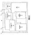
- control circuit 200 comprises a plurality of sub-circuits that includes a drive circuit 300, a turn-on synchronization circuit 400, a current mirror circuit 500, a rail voltage regulator circuit 600, a lamp current regulator circuit 700, and (optionally) a shutdown circuit 800.
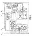
- Preferred circuitry for realizing each of the sub-circuits 300,400,500,600,700,800 is described in FIG. 3 .
- drive circuit 300 is coupled to each of the other sub-circuits 400,500,600,700,800 and to second connection 204 of control circuit 200. During operation, drive circuit 300 provides the control voltage (for switching FET 130 on and off) via second connection 204.
- Turn-on synchronization circuit 400 is coupled to drive circuit 3 00 and to first connection 202. During operation, turn-on synchronization circuit 400 monitors, via first connection 202, the drain-to-source voltage (V DS ) of FET 130 during the periods when FET 130 is off. When V DS swings low, turn-on synchronization circuit 400 directs drive circuit 300 to provide a positive control voltage (e.g., +10 volts or so) to switch FET 130 on. In this way, control circuit 200 provides energy efficient zero voltage switching of FET 130.
- V DS drain-to-source voltage
- Current mirror circuit 500 is coupled to drive circuit 300 and to first connection 202. During operation, current mirror circuit 500 effectively monitors, via first connection 202, the current that flows through primary winding 122 of transformer 120 during the periods when FET 130 is on. When the current through primary winding 122 reaches a predetermined peak threshold, current mirror circuit 500 directs drive circuit 300 to provide an approximately zero control voltage to switch FET 130 off.
- current mirror circuit 500 allows control circuit 200 to provide current-mode type control without requiring the presence of either a dissipative current-sensing resistor or an expensive current transformer. Thus, current mirror circuit enhances the energy efficiency and low material cost of ballast 10.
- Rail voltage regulator circuit 600 is coupled to fourth connection 208 and drive circuit 300. During operation, rail voltage regulator circuit 600 monitors V RAIL via fourth connection 208 and directs drive circuit 300 to adjust a duty cycle of the control voltage provided to FET 130 in order to maintain (regulate) V RAIL at a predetermined desired level (e.g., 400 volts).
- a predetermined desired level e.g. 400 volts.
- Lamp current regulator circuit 700 is coupled to third connection 206 and drive circuit 300. During operation, lamp current regulator circuit 700 monitors, via third connection 206, the voltage across resistor 180 (which, as previously explained, is indicative of the amount of current supplied to lamp 20), and directs drive circuit 300 to adjust the duty cycle of the control voltage provided to FET 130 in order to maintain (regulate) the lamp current at a pre-specified desired level.
- Shutdown circuit 800 is coupled to drive circuit 300.
- shutdown circuit 800 in response to a shutdown command (e.g., as provided by external protection circuitry, which is not shown or described herein, within switching converter 100 or inverter 900), shutdown circuit 800 directs drive circuit 300 to cease switching of FET 130, thereby protecting ballast 10 from possible damage in the event of a fault condition.
- a shutdown command e.g., as provided by external protection circuitry, which is not shown or described herein, within switching converter 100 or inverter 900
- shutdown circuit 800 directs drive circuit 300 to cease switching of FET 130, thereby protecting ballast 10 from possible damage in the event of a fault condition.
- shutdown circuit 800 is optional, as it is not required in order for control circuit 200 to serve its primary purpose of providing high frequency zero voltage switching.
- control circuit 200 Preferred circuitry for implementing control circuit 200 is now explained with reference to FIG. 3 , as follows:
- the RC time constant of resistor 360 and capacitor 370 places a limit upon the maximum time that transistor 130 can remain off.
- turn-on synchronization circuit 400 preferably comprises a transistor 410, a diode 420, a first resistor 430, a first capacitor 440, a second resistor 432, and a series combination of a third resistor 434 and a second capacitor 442.
- Transistor 410 is preferably implemented by a PNP type bipolar junction transistor (BJT) having a base 412, a collector 414, and an emitter 416.
- Emitter 416 is coupled to DC supply voltage
- V CC- Diode 420 and first resistor 430 are each coupled between emitter 416 and base 412 of BJT 410.
- First capacitor 440 is coupled between collector 414 of BJT 410 and first node 372 of drive circuit 300.
- Second resistor 432 is coupled between collector 414 of BJT 410 and circuit ground 60.
- the series combination of third resistor 434 and second capacitor 442 is coupled between base 412 of BJT 410 and first connection 202 of control circuit 200.
- current mirror circuit 500 preferably comprises a first transistor 510, a second transistor 520, a first resistor 530, a second resistor 534, a third resistor 536, a capacitor 540, a first diode 550, and a second diode 560.
- First transistor 510 is preferably implemented by a N-channel field effect transistor (FET) having a gate 512, a drain 514, and a source 516.
- Source 516 is coupled to circuit ground 60
- drain 514 is coupled to third pin 316 (labeled "CS") of PWM IC 310 of drive circuit 300.
- FET N-channel field effect transistor
- Second transistor 520 is preferably implemented by a N-channel field effect transistor (FET) having a gate 522, a drain 524, and a source 526.
- Source 526 is coupled to circuit ground 60
- drain 524 is coupled to gate 512 of FET 510.
- First resistor 530 is coupled between the DC supply voltage, V CC , and gate 512 of FET 510.
- Second resistor 534 is coupled between the DC supply voltage, V CC , and drain 514 of FET 510.
- Third resistor 536 is coupled between the DC supply voltage, V CC , and a first node 542.
- Capacitor 540 is coupled between drain 514 and source 516 of FET 510.
- First diode 550 is coupled between first node 542 and first connection 202 of control circuit 200.
- Second diode 560 is coupled between first node 542 and drain 514 of FET 510.
- the RC time constant of resistor 534 and capacitor 540 places a limit upon the maximum time that transistor 130 can remain on.
- rail voltage regulator circuit 600 preferably comprises an operational amplifier (OP AMP) 610, a first resistor 630, a second resistor 632, a third resistor 634, a fourth resistor 636, and a fifth resistor 638.
- OP AMP 610 has a non-inverting input 612, an inverting input 614, and an output 616.
- First resistor 630 is coupled between non-inverting input 612 and fourth connection 208 of control circuit 200.
- Second resistor 632 is coupled between non-inverting input 612 and circuit ground 60.
- Third resistor 634 is coupled between the reference voltage, V REF , and inverting input 614.
- Fourth resistor 636 is coupled between inverting input 614 and output 616.
- Fifth resistor 638 is coupled between output 616 and second pin 314 (labeled "V FB ") of PWM IC 310 of drive circuit 300.
- lamp current regulator circuit 700 preferably comprises a first operational amplifier (OP AMP) 710, a second OP AMP 720, a first resistor 730, a second resistor 732, a third resistor 734, a fourth resistor 736, a capacitor 740, and a fifth resistor 738.
- First OP AMP 710 has a non-inverting input 712, an inverting input 714, and an output 716.
- Non-inverting input 712 is coupled to circuit ground 60.
- Second OP AMP 720 has a non-inverting input 722, an inverting input 724, and an output 726.
- First resistor 730 is coupled between inverting input 714 of first OP AMP 710 and third connection 206 of control circuit 200.
- Second resistor 732 is coupled between inverting input 714 of OP AMP 710 and output 716 of OP AMO 710.
- Third resistor 734 is coupled between output 716 of OP AMP 710 and non-inverting input 722 of OP AMP 720.
- Fourth resistor 736 is coupled between a lamp current reference voltage, V I , and inverting input 724 of OP AMP 720; the lamp current, reference voltage, V I , is provided by other circuitry (not shown or described herein) within ballast 10 in order to specify a desired level for the current provided to lamp 20.
- Capacitor 740 is coupled between inverting input 724 of OP AMP 720 and output 726 of OP AMP 720.
- Fifth resistor 738 is coupled between output 726 of OP AMP 720 and second pin 314 (labeled "V FB ”) of PWM IC 310 of drive circuit 300.
- shutdown circuit 800 preferably comprises a transistor 810 and a resistor 820.
- Transistor 810 is preferably realized by a NPN-type bipolar junction transistor having a base 812, a collector 814, and an emitter 816.
- Base 812 is coupled to a shutdown signal, VSD, that is provided by protective circuitry (not shown or described herein) within switching converter 100 or inverter 900.
- Collector 814 is coupled to first pin 312 (labeled "COMP") of PWM IC 310 of drive circuit 300.
- Emitter 816 is coupled to circuit ground 60.
- Resistor 820 is coupled between the DC supply voltage, V CC , and base 812 of transistor 810.
Landscapes
- Circuit Arrangements For Discharge Lamps (AREA)
- Dc-Dc Converters (AREA)
Description
- The present invention relates to the general subject of circuits for powering discharge lamps. More particularly, the present invention relates to a ballast that includes a switching converter having a novel control circuit for providing zero voltage switching.
- The present application claims priority to
U.S. Provisional Patent Application Serial No. 60/621,213 - A need exists for a ballast that includes a zero voltage switching converter that is capable of operating at a very high frequency (e.g., up to 900 kilohertz) and that includes a control circuit that may be implemented using standard (i.e., "off-the-shelf") components. Zero voltage switching (ZVS) is desirable because it reduces switching power losses in the converter transistor and thus enhances the overall energy efficiency of the ballast. Standard components are preferred due to a number of practical considerations, including material cost, part availability, and design flexibility. High frequency operation is desirable because it makes possible the use of planar type magnetic components (instead of conventional core-and-bobbin type components) and the elimination of large electrolytic capacitors (which are physically large and which tend to significantly detract from the useful operating life of the ballast). Such a ballast, in comparison with existing ballasts, would provide higher energy efficiency, reduced physical size, material cost, enhanced operating life, and lower material cost, and would thus represent a significant advance over the prior art.
- From
US 6 826 063 B2 a DC Voltage converting circuit according to the preamble of the independent claim is known. The switching Frequency is changed according to a current flowing through the primary and the secondary windings of the converter Transformer. -
US 6 548 966 B2 discloses a discharge lamp lighting device with a converting circuit featuring a switch that is controlled by a PWM scheme. -
-
FIG. 1 is a block diagram schematic of a ballast that includes a switching converter and an inverter, in accordance with a preferred embodiment of the present invention. -
FIG. 2 is a block-diagram schematic of a control circuit for the switching converter described inFIG. 1 , in accordance with a preferred embodiment of the present invention. -
FIG. 3 is a detailed electrical schematic of the control circuit described inFIG. 2 , in accordance with a preferred embodiment of the present invention. -
FIG. 1 describes aballast 10 for powering at least onedischarge lamp 20, such as a high-intensity discharge (HID) lamp: Ballast 10 comprises aswitching converter 100 and aninverter 900. During operation,switching converter 100 receives an input voltage, VIN, and provides a substantially direct current (DC) rail voltage, VRAIL, to inverter 900.Inverter 900 receives VRAIL and provides periodically alternating output voltage and output current for igniting and poweringlamp 20. - As described in
FIG. 1 ,switching converter 100 is preferably realized as flyback type converter comprising first and second input terminals 102,104, first and second output terminals 106,108, afirst capacitor 110, atransformer 120, atransistor 130, a series combination of asecond capacitor 140 and afirst resistor 142, adiode 150, athird capacitor 160, afourth capacitor 170, asecond resistor 180, and acontrol circuit 200.First capacitor 110 is coupled between first and second input terminals 102,104.Second input terminal 104 andsecond output terminal 108 are each coupled tocircuit ground 60. Transformer 120 includes aprimary winding 122 and asecondary winding 124.Transistor 130 is coupled in series withprimary winding 122 oftransformer 120, and is preferably implemented by a N-channel field effect transistor (FET) having agate terminal 132, adrain terminal 134, and asource terminal 136.Primary winding 122 oftransformer 120 is coupled betweenfirst input terminal 102 anddrain 134 ofFET 130.Source 136 of FET 130 is coupled tocircuit ground 60. The series combination ofsecond capacitor 140 andfirst resistor 142 is coupled betweendrain terminals 134 andcircuit ground 60.Secondary winding 124 oftransformer 120 is coupled between afirst node 162 and asecond node 172.Diode 150 andthird capacitor 160 are each coupled betweenfirst node 162 andfirst output terminal 106.Fourth capacitor 170 is coupled betweenfirst output terminal 106 andsecond node 172. Finally,second resistor 180 is coupled betweensecond node 172 andcircuit ground 60. - During operation of switching
converter 100, FET 130 is turned on and off in a controlled manner bycontrol circuit 200 so as to provide a regulated DC rail voltage (i.e., VRAIL, which is typically designed to be on the order of about 400 volts), as well as a limited current, to inverter 900 for powering lamp 2 0 at a desired level.Control circuit 200 further operates to provide substantially zero voltage switching ofFET 130, thereby minimizing the switching power losses inFET 130 and enhancing the overall energy efficiency ofballast 10. Additionally,control circuit 200 is intended to drive FET 130 at a very high frequency (e.g., 900 kilohertz) so as to allow for the use of planar magnetic components (e.g., for implementing transformer 120) and to eliminate any need for large electrolytic capacitors (e.g., for implementing capacitor 170), thereby reducing the size and weight, and enhancing the expected operating life, ofballast 10. - As described in
FIG 1 ,inverter 900 is preferably implemented as a full-bridge type inverter having first and second output connections 902,904, first, second, third, and fourth transistors 910,920,930,940 (preferably implemented by N-channel FETs), first and second inductors 950,970, and acapacitor 960. FET 910 is coupled between first output terminal 106 (of converter 100) and afirst node 912. FET 920 is coupled betweenfirst node 912 andcircuit ground 60. FET 930 is coupled between first output terminal 106 (of converter 100) and asecond node 932. FET 940 is coupled betweensecond node 932 andcircuit ground 60.First inductor 950 is coupled betweenfirst node 912 andsecond output connection 904. Capacitor 90 is coupled between first and second output connections 902,904. Finally,second inductor 970 is coupled betweensecond node 932 andfirst output connection 902. - It should be understood that
inverter 900 requires an inverter driver circuit (not shown or described inFIG. 1 ) for commutating FETs 910,920,930,940 in a controlled complementary fashion (i.e., so that when FETs 910,940 are on, FETs 920,930 are off, and vice-versa). An appropriate driver circuit forinverter 900 may be realized by any of a number of arrangements that are well known to those skilled in the art of lighting ballasts and/or power supplies. - Referring again to
FIG. 1 ,control circuit 200 includes first, second, third, and fourth connections 202,204,206,208 that are coupled to different points withinswitching converter 100. More specifically,first connection 202 is coupled todrain terminal 134 of FET 130,second connection 204 is coupled togate terminal 132 of FET 130,third connection 206 is coupled tosecond node 172, andfourth connection 208 is coupled tofirst output terminal 208. During operation,control circuit 200 monitors, viafirst connection 202, the voltage, VDS, between the drain and source terminals 134,136 ofFET 130 when FET 130 is off. Control circuit also monitors, viafirst connection 202, the current, IP, that flows throughprimary winding 122 oftransformer 120 when FET 130 is on. A control signal for switchingFET 130 on and off is provided bycontrol circuit 200 viasecond connection 204.Control circuit 200 monitors, viathird connection 206, the voltage acrossresistor 180; the voltage acrossresistor 180 is proportional to the output current provided by switchingconverter 100 and is related to the amount of current ultimately provided tolamp 20 byinverter 900. Finally,control circuit 200 monitors the DC rail voltage, VRAIL, by way offourth connection 208. - Referring now to
FIG. 2 , in a preferred embodiment of the present invention,control circuit 200 comprises a plurality of sub-circuits that includes adrive circuit 300, a turn-onsynchronization circuit 400, acurrent mirror circuit 500, a railvoltage regulator circuit 600, a lampcurrent regulator circuit 700, and (optionally) ashutdown circuit 800. Preferred circuitry for realizing each of the sub-circuits 300,400,500,600,700,800 is described inFIG. 3 . - As illustrated in
FIG. 2 ,drive circuit 300 is coupled to each of the other sub-circuits 400,500,600,700,800 and tosecond connection 204 ofcontrol circuit 200. During operation,drive circuit 300 provides the control voltage (for switchingFET 130 on and off) viasecond connection 204. - Turn-on
synchronization circuit 400 is coupled to drive circuit 3 00 and tofirst connection 202. During operation, turn-onsynchronization circuit 400 monitors, viafirst connection 202, the drain-to-source voltage (VDS) ofFET 130 during the periods when FET 130 is off. When VDS swings low, turn-onsynchronization circuit 400directs drive circuit 300 to provide a positive control voltage (e.g., +10 volts or so) to switchFET 130 on. In this way,control circuit 200 provides energy efficient zero voltage switching ofFET 130. -
Current mirror circuit 500 is coupled to drivecircuit 300 and tofirst connection 202. During operation,current mirror circuit 500 effectively monitors, viafirst connection 202, the current that flows throughprimary winding 122 oftransformer 120 during the periods when FET 130 is on. When the current throughprimary winding 122 reaches a predetermined peak threshold,current mirror circuit 500 directsdrive circuit 300 to provide an approximately zero control voltage to switchFET 130 off. Advantageously,current mirror circuit 500 allowscontrol circuit 200 to provide current-mode type control without requiring the presence of either a dissipative current-sensing resistor or an expensive current transformer. Thus, current mirror circuit enhances the energy efficiency and low material cost ofballast 10. - Rail
voltage regulator circuit 600 is coupled tofourth connection 208 and drivecircuit 300. During operation, railvoltage regulator circuit 600 monitors VRAIL viafourth connection 208 and directsdrive circuit 300 to adjust a duty cycle of the control voltage provided toFET 130 in order to maintain (regulate) VRAIL at a predetermined desired level (e.g., 400 volts). - Lamp
current regulator circuit 700 is coupled tothird connection 206 and drivecircuit 300. During operation, lampcurrent regulator circuit 700 monitors, viathird connection 206, the voltage across resistor 180 (which, as previously explained, is indicative of the amount of current supplied to lamp 20), and directsdrive circuit 300 to adjust the duty cycle of the control voltage provided toFET 130 in order to maintain (regulate) the lamp current at a pre-specified desired level. -
Shutdown circuit 800 is coupled to drivecircuit 300. During operation, in response to a shutdown command (e.g., as provided by external protection circuitry, which is not shown or described herein, within switchingconverter 100 or inverter 900),shutdown circuit 800 directsdrive circuit 300 to cease switching ofFET 130, thereby protectingballast 10 from possible damage in the event of a fault condition. It should be appreciated thatshutdown circuit 800 is optional, as it is not required in order forcontrol circuit 200 to serve its primary purpose of providing high frequency zero voltage switching. - Preferred circuitry for implementing
control circuit 200 is now explained with reference toFIG. 3 , as follows: -
Drive circuit 300 preferably comprises a pulse-width modulation integrated circuit (PWM IC) 310, afirst resistor 330, afirst capacitor 332, atransistor 340, adiode 350, asecond resistor 360, athird resistor 362, afourth resistor 364, and acapacitor 370.PWM IC 310 comprises a first, second, third, fourth, fifth, sixth, seventh, and eight pins 312,314,316,318,320,322,324,326. Preferably,PWM IC 310 is realized by a commercially available integrated circuit, such as the UCC2803 pulse width modulation integrated circuit. The functions of the eight pins ofPWM IC 310 are denoted by the text labels inFIG. 3 , and are well understood by those skilled in the art; for example,first pin 312 is labeled "COMP,"second pin 314 is labeled "VFB," and so forth. Fifth pin 320 (labeled "GND") is coupled tocircuit ground 60. Seventh pin 324 (labeled "VCC") is coupled to a DC supply voltage, VCC, which is typically chosen to be on the order of about 12 volts.Eighth pin 326 is coupled to a reference voltage, VREF, which is typically chosen to be on the order of about 4 volts.First resistor 330 andfirst capacitor 332 are each coupled between first and second pins 312,314 ofPWM IC 310.Transistor 340 is preferably implemented by a N-channel field effect transistor (FET) having agate 342, adrain 344, and asource 346.Source 346 is coupled tocircuit ground 60.Diode 350 is coupled between the reference voltage, VREF, and fourth pin 318 (labeled "RT/CT") ofPWM IC 310.Second resistor 360 is coupled betweendiode 350 and drain 344 ofFET 340.Third resistor 362 is coupled between afirst node 372 andcircuit ground 60.Fourth resistor 364 is coupled betweengate 342 ofFET 340 and sixth pin 322 (labeled "OUT") ofPWM IC 310. Finally,capacitor 370 is coupled betweenfirst node 372 and drain 344 ofFET 340. - During operation of
drive circuit 300, the RC time constant ofresistor 360 andcapacitor 370 places a limit upon the maximum time thattransistor 130 can remain off. - Referring again to
FIG. 3 , turn-onsynchronization circuit 400 preferably comprises atransistor 410, adiode 420, afirst resistor 430, afirst capacitor 440, asecond resistor 432, and a series combination of athird resistor 434 and asecond capacitor 442.Transistor 410 is preferably implemented by a PNP type bipolar junction transistor (BJT) having a base 412, acollector 414, and anemitter 416.Emitter 416 is coupled to DC supply voltage, VCC- Diode 420 andfirst resistor 430 are each coupled betweenemitter 416 andbase 412 ofBJT 410.First capacitor 440 is coupled betweencollector 414 ofBJT 410 andfirst node 372 ofdrive circuit 300.Second resistor 432 is coupled betweencollector 414 ofBJT 410 andcircuit ground 60. The series combination ofthird resistor 434 andsecond capacitor 442 is coupled betweenbase 412 ofBJT 410 andfirst connection 202 ofcontrol circuit 200. - As described in
FIG. 3 ,current mirror circuit 500 preferably comprises afirst transistor 510, asecond transistor 520, afirst resistor 530, asecond resistor 534, athird resistor 536, acapacitor 540, afirst diode 550, and asecond diode 560.First transistor 510 is preferably implemented by a N-channel field effect transistor (FET) having agate 512, adrain 514, and asource 516.Source 516 is coupled tocircuit ground 60, and drain 514 is coupled to third pin 316 (labeled "CS") ofPWM IC 310 ofdrive circuit 300.Second transistor 520 is preferably implemented by a N-channel field effect transistor (FET) having a gate 522, a drain 524, and asource 526.Source 526 is coupled tocircuit ground 60, and drain 524 is coupled togate 512 ofFET 510.First resistor 530 is coupled between the DC supply voltage, VCC, andgate 512 ofFET 510.Second resistor 534 is coupled between the DC supply voltage, VCC, and drain 514 ofFET 510.Third resistor 536 is coupled between the DC supply voltage, VCC, and afirst node 542.Capacitor 540 is coupled betweendrain 514 andsource 516 ofFET 510.First diode 550 is coupled betweenfirst node 542 andfirst connection 202 ofcontrol circuit 200.Second diode 560 is coupled betweenfirst node 542 and drain 514 ofFET 510. - During operation of
current mirror circuit 500, the RC time constant ofresistor 534 andcapacitor 540 places a limit upon the maximum time thattransistor 130 can remain on. - Referring again to
FIG. 3 , railvoltage regulator circuit 600 preferably comprises an operational amplifier (OP AMP) 610, afirst resistor 630, asecond resistor 632, athird resistor 634, afourth resistor 636, and afifth resistor 638.OP AMP 610 has anon-inverting input 612, an invertinginput 614, and anoutput 616.First resistor 630 is coupled betweennon-inverting input 612 andfourth connection 208 ofcontrol circuit 200.Second resistor 632 is coupled betweennon-inverting input 612 andcircuit ground 60.Third resistor 634 is coupled between the reference voltage, VREF, and invertinginput 614.Fourth resistor 636 is coupled between invertinginput 614 andoutput 616.Fifth resistor 638 is coupled betweenoutput 616 and second pin 314 (labeled "VFB") ofPWM IC 310 ofdrive circuit 300. - As described in
FIG. 3 , lampcurrent regulator circuit 700 preferably comprises a first operational amplifier (OP AMP) 710, asecond OP AMP 720, afirst resistor 730, asecond resistor 732, athird resistor 734, afourth resistor 736, acapacitor 740, and afifth resistor 738.First OP AMP 710 has anon-inverting input 712, an invertinginput 714, and anoutput 716.Non-inverting input 712 is coupled tocircuit ground 60.Second OP AMP 720 has anon-inverting input 722, an invertinginput 724, and anoutput 726.First resistor 730 is coupled between invertinginput 714 offirst OP AMP 710 andthird connection 206 ofcontrol circuit 200.Second resistor 732 is coupled between invertinginput 714 ofOP AMP 710 andoutput 716 ofOP AMO 710.Third resistor 734 is coupled betweenoutput 716 ofOP AMP 710 andnon-inverting input 722 ofOP AMP 720.Fourth resistor 736 is coupled between a lamp current reference voltage, VI, and invertinginput 724 ofOP AMP 720; the lamp current, reference voltage, VI, is provided by other circuitry (not shown or described herein) withinballast 10 in order to specify a desired level for the current provided tolamp 20.Capacitor 740 is coupled between invertinginput 724 ofOP AMP 720 andoutput 726 ofOP AMP 720.Fifth resistor 738 is coupled betweenoutput 726 ofOP AMP 720 and second pin 314 (labeled "VFB") ofPWM IC 310 ofdrive circuit 300. - Referring again to
FIG. 3 ,shutdown circuit 800 preferably comprises atransistor 810 and aresistor 820.Transistor 810 is preferably realized by a NPN-type bipolar junction transistor having a base 812, acollector 814, and anemitter 816.Base 812 is coupled to a shutdown signal, VSD, that is provided by protective circuitry (not shown or described herein) within switchingconverter 100 orinverter 900.Collector 814 is coupled to first pin 312 (labeled "COMP") ofPWM IC 310 ofdrive circuit 300.Emitter 816 is coupled tocircuit ground 60.Resistor 820 is coupled between the DC supply voltage, VCC, andbase 812 oftransistor 810. - Although the present invention has been described with reference to certain preferred embodiments, numerous modifications and variations can be made by those skilled in the art without departing from the novel spirit and scope of this invention.
Claims (13)
- A ballast (10) for powering at least one discharge lamp (20); comprising:an inverter (900) having output connections (902, 904) adapted for coupling to the at least one discharge lamp (20); anda switching converter (100) for providing a substantially direct current (DC) rail voltage (Vrail), comprising:first and second input terminals (102, 104) for receiving an input voltage (Vin),first and second output terminals (106, 108) coupled to the inverter (900), wherein the DC rail voltage (Vrail) is provided between the first and second output terminals (106,108),a transformer (120) having a primary winding (122) and a secondary winding (124);a transistor (130) having a gate terminal, a drain terminal, and a source terminal, wherein the drain terminal is coupled to the primary winding (122) of the transformer (120) and the source terminal is coupled to circuit ground (60), anda control circuit (200) coupled to the transistor (130) characterized in that said control circuit (200) is operable to provide substantially zero voltage switching (ZVS) of the transistor (130), the control circuit comprising:a first connection (202) coupled to the drain terminal of the transistor (130), a second connection (204) coupled to the gate terminal of the transistor (130), a third connection (206) coupled to the secondary winding (124) of the transformer (124), and a fourth connection (208) coupled to the first output terminal (206);a drive circuit (300) coupled to the first and second connections (202, 204); and operable to provide an output signal for turning the transistor (130) on and off;a turn-on synchronization circuit (400) coupled to the first connection (202) and to the drive circuit (300), wherein the turn-on synchronization circuit (400) is operable to monitor a voltage between the drain and source terminals of the transistor (130) and, in response to the voltage between the drain and source terminals approaching zero, to direct the drive circuit turn the transistor (130) on;a current mirror circuit (500) coupled to the first connection (202) and to the drive circuit (300), wherein the current mirror circuit (500) is operable to monitor a current through the primary winding (122) of the transformer (120) and, in response to the current through the primary winding (122) reaching a predetermined peak level, to direct the drive circuit to turn the transistor (130) off;a rail voltage regulator circuit (600) coupled to the fourth connection (208) and to the drive circuit (300) wherein the rail voltage regulator circuit (600) is operable to monitor the rail voltage (Vrail) and to control the output signal of the drive circuit (300) so as to maintain the rail voltage (Vrail) at a first predetermined level; anda lamp current regulator circuit (700) coupled to the third connection (206) and to the drive circuit (300), wherein lamp current regulator circuit (700) is operable to monitor the output current of the switching converter (100) and to control the output signal of the drive circuit (300) so as to maintain the output current at a second predetermined level.
- The ballast (10) of claim 1, wherein:the secondary winding (124) of the transformer (120) is coupled between a first node and a second node (162, 172);the switching converter (160) further comprises:a first capacitor (110) coupled between the first and second input terminals (102, 104);a series combination of a second capacitor (140) and a first resistor (142), the series combination being coupled between the drain terminal of the transistor (130) and circuit ground;a diode (150) coupled between the first node (162) and the first output terminal (106);a third capacitor (160) coupled between the first node (162) and the first output terminal (106);a fourth capacitor (170) coupled between the first output terminal (106) and the second node (172), anda second resistor (180) coupled between the second node (172) and circuit ground; andthe third connection (206) of the control circuit (200) is coupled to the second node (172).
- The ballast (10) of claim 1, wherein the drive circuit (300) comprises:a pulse-width modulation integrated circuit (PWM IC) comprising first, second, third, fourth, fifth, sixth, seventh, and eighth pins, wherein the fifth pin is coupled to circuit ground, the seventh pin is coupled to a DC supply voltage, and the eighth pin is coupled to a reference voltage;a first resistor coupled between the first and second pins of the PWM IC;a first capacitor coupled between the first and second pins of the PWM IC;a transistor having a gate, a drain, and a source, wherein the source is coupled to circuit ground (60);a diode coupled between the reference voltage and the fourth pin of the PWM IC;a second resistor coupled between the diode and the drain of the transistor;a third resistor coupled between a first node and circuit ground;a fourth resistor coupled between the gate of the transistor and the sixth pin of the PWM IC; anda capacitor coupled between the first node and the drain of the transistor.
- The ballast of claim 3, wherein the transistor of the drive circuit is a N-channel field effect transistor.
- The ballast (10) of claim 3, wherein the turn-on synchronization circuit (400) comprises:a transistor (410) having a base, a collector, and an emitter, wherein the emitter is coupled to the DC supply voltage (Vcc);a diode (420) coupled between the emitter and the base of the transistor (410);a first resistor coupled between the emitter and the base of the transistor;a first capacitor coupled between the collector of the transistor and the first node of the drive circuit;a second resistor coupled between the collector of the transistor and circuit ground; anda series combination of a third resistor and a second capacitor coupled between the base of the transistor and the first connection of the control circuit.
- The ballast (10) of claim 5, wherein the transistor (410) of the turn-on synchronization circuit is PNP-type bipolar junction transistor.
- The ballast (10) of claim 3, wherein the current mirror (500) circuit comprises:a first transistor having a gate, a drain, and a source, wherein the source is coupled to circuit ground and the drain is coupled to the third pin of the PWM IC of the drive circuit;a second transistor having a gate, a drain, and a source, wherein the source is coupled to circuit ground and the drain is coupled to the gate of the first transistor;a first resistor coupled between the DC supply voltage and the gate of the first transistor;a second resistor coupled between the DC supply voltage and the drain of the first transistor;a third resistor coupled between the DC supply voltage and a first node;a capacitor coupled between the drain and the source of the first transistor;a first diode coupled between the first node and the first connection of the control circuit; anda second diode coupled between the first node and the drain of the first transistor.
- The ballast (10) of claim 7, wherein the first transistor and the second transistor of the current mirror circuit are each N-channel field effect transistors.
- The ballast (10) of claim 3, wherein the rail voltage regulator circuit (600) comprises:an operational amplifier (610) having a non-inverting input, an inverting input, and an output;a first resistor coupled between the fourth connection of the control circuit and the non-inverting input of the operational amplifier;a second resistor coupled between the non-inverting input of the operational amplifier and circuit ground;a third resistor coupled between the reference voltage and the inverting input of the operational amplifier;a fourth resistor coupled between the inverting input and the output of the operational amplifier; anda fifth resistor coupled between the output of the operational amplifier and the second pin of the PWM IC of the drive circuit.
- The ballast (10) of claim 3, wherein the lamp current regulator circuit (700) comprises:a first operational amplifier having a non-inverting input, an inverting input, and an output, wherein the non-inverting input is coupled to circuit ground;a second operational amplifier having a non-inverting input, an inverting input, and an output;a first resistor coupled between the third connection of the control circuit and the inverting input of the first operational amplifier;a second resistor coupled between the inverting input of the first operational amplifier and the output of the first operational amplifier;a third resistor coupled between the output of the first operational amplifier and the non-inverting input of the second operating amplifier;a fourth resistor coupled between a lamp current reference voltage and the inverting input of the second operational amplifier;a capacitor coupled between the inverting input of the second operational amplifier and the output of the second operational amplifier; anda fifth resistor coupled between the output of the second operational amplifier and the second pin of the PWM IC of the drive circuit.
- The ballast (10) of claim 3, wherein the control circuit (200) further comprises a shutdown circuit that is operable, in response to a shutdown command, to direct the drive circuit to cease switching of the transistor of the switching converter.
- The ballast (10) of claim 11, wherein the shutdown circuit (800) comprises:a transistor (810) having a base, a collector, and an emitter, wherein the base is coupled to a shutdown signal, the collector is coupled to the first pin of the PWM IC of the drive circuit, and the emitter is coupled to circuit ground; anda resistor coupled between the DC supply voltage and the base of the transistor.
- The ballast (10) of claim 12, wherein the transisior (810) of the shutdown circuit (800) is a NPN-type bipolar junction transistor.
Applications Claiming Priority (2)
| Application Number | Priority Date | Filing Date | Title |
|---|---|---|---|
| US62121304P | 2004-10-22 | 2004-10-22 | |
| PCT/US2005/037717 WO2006047210A2 (en) | 2004-10-22 | 2005-10-21 | Ballast with zero voltage switching converter |
Publications (3)
| Publication Number | Publication Date |
|---|---|
| EP1803335A2 EP1803335A2 (en) | 2007-07-04 |
| EP1803335A4 EP1803335A4 (en) | 2013-11-20 |
| EP1803335B1 true EP1803335B1 (en) | 2015-01-07 |
Family
ID=36228251
Family Applications (1)
| Application Number | Title | Priority Date | Filing Date |
|---|---|---|---|
| EP05838124.5A Expired - Lifetime EP1803335B1 (en) | 2004-10-22 | 2005-10-21 | Ballast with zero voltage switching converter |
Country Status (4)
| Country | Link |
|---|---|
| US (1) | US7402956B2 (en) |
| EP (1) | EP1803335B1 (en) |
| JP (1) | JP4499793B2 (en) |
| WO (1) | WO2006047210A2 (en) |
Families Citing this family (3)
| Publication number | Priority date | Publication date | Assignee | Title |
|---|---|---|---|---|
| US7376770B2 (en) | 2005-02-25 | 2008-05-20 | International Business Machines Corporation | System and method for virtual adapter resource allocation matrix that defines the amount of resources of a physical I/O adapter |
| JP2010512636A (en) * | 2006-12-12 | 2010-04-22 | コーニンクレッカ フィリップス エレクトロニクス エヌ ヴィ | Lamp driver for operating gas discharge lamp |
| JP2009032600A (en) * | 2007-07-28 | 2009-02-12 | Funai Electric Co Ltd | Power supply for fluorescent tube, backlight |
Family Cites Families (11)
| Publication number | Priority date | Publication date | Assignee | Title |
|---|---|---|---|---|
| US6057652A (en) * | 1995-09-25 | 2000-05-02 | Matsushita Electric Works, Ltd. | Power supply for supplying AC output power |
| US6300725B1 (en) * | 1997-06-16 | 2001-10-09 | Lightech Electronics Industries Ltd. | Power supply for hybrid illumination system |
| US6469454B1 (en) * | 2000-06-27 | 2002-10-22 | Maxim Integrated Products, Inc. | Cold cathode fluorescent lamp controller |
| JP2002352989A (en) * | 2001-05-25 | 2002-12-06 | Mitsubishi Electric Corp | Discharge lamp lighting device |
| JP4023114B2 (en) * | 2001-07-13 | 2007-12-19 | 松下電工株式会社 | Discharge lamp lighting device |
| JP3610383B2 (en) * | 2002-01-16 | 2005-01-12 | オリジン電気株式会社 | Flyback converter |
| JP3839737B2 (en) * | 2002-03-01 | 2006-11-01 | 株式会社小糸製作所 | DC voltage conversion circuit |
| JP2004282868A (en) * | 2003-03-14 | 2004-10-07 | Origin Electric Co Ltd | Switching power supply circuit |
| US7265503B2 (en) * | 2004-04-08 | 2007-09-04 | International Rectifier Corporation | Applications of halogen convertor control IC |
| US7095183B2 (en) * | 2004-07-07 | 2006-08-22 | Osram Sylvania Inc. | Control system for a resonant inverter with a self-oscillating driver |
| US7030570B2 (en) * | 2004-07-07 | 2006-04-18 | Osram Sylvania Inc. | Resonant inverter including feed back circuit with source of variable bias current |
-
2005
- 2005-10-21 WO PCT/US2005/037717 patent/WO2006047210A2/en not_active Ceased
- 2005-10-21 JP JP2007538022A patent/JP4499793B2/en not_active Expired - Fee Related
- 2005-10-21 EP EP05838124.5A patent/EP1803335B1/en not_active Expired - Lifetime
- 2005-10-21 US US11/660,789 patent/US7402956B2/en not_active Expired - Fee Related
Also Published As
| Publication number | Publication date |
|---|---|
| WO2006047210A2 (en) | 2006-05-04 |
| WO2006047210A3 (en) | 2006-06-22 |
| EP1803335A2 (en) | 2007-07-04 |
| JP4499793B2 (en) | 2010-07-07 |
| US7402956B2 (en) | 2008-07-22 |
| EP1803335A4 (en) | 2013-11-20 |
| JP2008517444A (en) | 2008-05-22 |
| US20080061706A1 (en) | 2008-03-13 |
Similar Documents
| Publication | Publication Date | Title |
|---|---|---|
| EP2845301B1 (en) | Driver circuits for dimmable solid state lighting apparatus | |
| US9706614B2 (en) | Illumination systems | |
| EP1579735B1 (en) | Leds driver | |
| US6870326B1 (en) | Fluorescent ballast with isolated system interface | |
| EP2298030B1 (en) | Led lamp driver and method | |
| TWI411207B (en) | Resonant driver with low-voltage secondary side control for high power led lighting | |
| US20120319604A1 (en) | Cascade boost and inverting buck converter with independent control | |
| US11223271B2 (en) | Gate drive adapter | |
| KR20080087819A (en) | Method and apparatus for controlling the current supplied to an electronic device | |
| WO2012016207A1 (en) | Multiple power sources for a switching power converter controller | |
| US6194845B1 (en) | Ballasts with tapped inductor arrangements for igniting and powering high intensity discharge lamps | |
| US20040246748A1 (en) | Bridge-buck converter with self-driven synchronous rectifiers | |
| US9780690B2 (en) | Resonant decoupled auxiliary supply for a switched-mode power supply controller | |
| EP1413177A1 (en) | Overvoltage protection for hid lamp ballast | |
| EP2070171A2 (en) | Inverter with improved overcurrent protection circuit, and power supply and electronic ballast therefor | |
| US6107750A (en) | Converter/inverter circuit having a single switching element | |
| US5729098A (en) | Power supply and electronic ballast with a novel boost converter control circuit | |
| US7402956B2 (en) | Ballast with zero voltage switching converter | |
| US8766672B2 (en) | Electronic switching device | |
| US20230422375A1 (en) | Power control device | |
| US20110260640A1 (en) | Power supply circuit for light sources, such as lighting led systems | |
| KR20020073756A (en) | Protective circuit for ballast high pressure discharge lamp | |
| US10390391B2 (en) | Driver for a light emitting diode (LED) lighting system | |
| KR200235270Y1 (en) | Protective circuit for ballast high pressure discharge lamp | |
| KR200222419Y1 (en) | Direct current amplifier converting apparatus |
Legal Events
| Date | Code | Title | Description |
|---|---|---|---|
| PUAI | Public reference made under article 153(3) epc to a published international application that has entered the european phase |
Free format text: ORIGINAL CODE: 0009012 |
|
| 17P | Request for examination filed |
Effective date: 20070301 |
|
| AK | Designated contracting states |
Kind code of ref document: A2 Designated state(s): AT BE BG CH CY CZ DE DK EE ES FI FR GB GR HU IE IS IT LI LT LU LV MC NL PL PT RO SE SI SK TR |
|
| DAX | Request for extension of the european patent (deleted) | ||
| A4 | Supplementary search report drawn up and despatched |
Effective date: 20131018 |
|
| RIC1 | Information provided on ipc code assigned before grant |
Ipc: H05B 37/02 20060101AFI20131014BHEP Ipc: H05B 41/288 20060101ALI20131014BHEP |
|
| RIC1 | Information provided on ipc code assigned before grant |
Ipc: H05B 37/02 20060101AFI20140619BHEP Ipc: H05B 41/288 20060101ALI20140619BHEP |
|
| GRAP | Despatch of communication of intention to grant a patent |
Free format text: ORIGINAL CODE: EPIDOSNIGR1 |
|
| INTG | Intention to grant announced |
Effective date: 20140909 |
|
| GRAS | Grant fee paid |
Free format text: ORIGINAL CODE: EPIDOSNIGR3 |
|
| GRAA | (expected) grant |
Free format text: ORIGINAL CODE: 0009210 |
|
| AK | Designated contracting states |
Kind code of ref document: B1 Designated state(s): AT BE BG CH CY CZ DE DK EE ES FI FR GB GR HU IE IS IT LI LT LU LV MC NL PL PT RO SE SI SK TR |
|
| REG | Reference to a national code |
Ref country code: GB Ref legal event code: FG4D |
|
| REG | Reference to a national code |
Ref country code: CH Ref legal event code: EP |
|
| REG | Reference to a national code |
Ref country code: IE Ref legal event code: FG4D |
|
| REG | Reference to a national code |
Ref country code: AT Ref legal event code: REF Ref document number: 706493 Country of ref document: AT Kind code of ref document: T Effective date: 20150215 |
|
| REG | Reference to a national code |
Ref country code: DE Ref legal event code: R096 Ref document number: 602005045644 Country of ref document: DE Effective date: 20150226 |
|
| REG | Reference to a national code |
Ref country code: NL Ref legal event code: VDEP Effective date: 20150107 |
|
| REG | Reference to a national code |
Ref country code: AT Ref legal event code: MK05 Ref document number: 706493 Country of ref document: AT Kind code of ref document: T Effective date: 20150107 |
|
| REG | Reference to a national code |
Ref country code: LT Ref legal event code: MG4D |
|
| PG25 | Lapsed in a contracting state [announced via postgrant information from national office to epo] |
Ref country code: SE Free format text: LAPSE BECAUSE OF FAILURE TO SUBMIT A TRANSLATION OF THE DESCRIPTION OR TO PAY THE FEE WITHIN THE PRESCRIBED TIME-LIMIT Effective date: 20150107 Ref country code: LT Free format text: LAPSE BECAUSE OF FAILURE TO SUBMIT A TRANSLATION OF THE DESCRIPTION OR TO PAY THE FEE WITHIN THE PRESCRIBED TIME-LIMIT Effective date: 20150107 Ref country code: FI Free format text: LAPSE BECAUSE OF FAILURE TO SUBMIT A TRANSLATION OF THE DESCRIPTION OR TO PAY THE FEE WITHIN THE PRESCRIBED TIME-LIMIT Effective date: 20150107 Ref country code: BG Free format text: LAPSE BECAUSE OF FAILURE TO SUBMIT A TRANSLATION OF THE DESCRIPTION OR TO PAY THE FEE WITHIN THE PRESCRIBED TIME-LIMIT Effective date: 20150407 Ref country code: ES Free format text: LAPSE BECAUSE OF FAILURE TO SUBMIT A TRANSLATION OF THE DESCRIPTION OR TO PAY THE FEE WITHIN THE PRESCRIBED TIME-LIMIT Effective date: 20150107 |
|
| PG25 | Lapsed in a contracting state [announced via postgrant information from national office to epo] |
Ref country code: NL Free format text: LAPSE BECAUSE OF FAILURE TO SUBMIT A TRANSLATION OF THE DESCRIPTION OR TO PAY THE FEE WITHIN THE PRESCRIBED TIME-LIMIT Effective date: 20150107 Ref country code: AT Free format text: LAPSE BECAUSE OF FAILURE TO SUBMIT A TRANSLATION OF THE DESCRIPTION OR TO PAY THE FEE WITHIN THE PRESCRIBED TIME-LIMIT Effective date: 20150107 Ref country code: IS Free format text: LAPSE BECAUSE OF FAILURE TO SUBMIT A TRANSLATION OF THE DESCRIPTION OR TO PAY THE FEE WITHIN THE PRESCRIBED TIME-LIMIT Effective date: 20150507 Ref country code: GR Free format text: LAPSE BECAUSE OF FAILURE TO SUBMIT A TRANSLATION OF THE DESCRIPTION OR TO PAY THE FEE WITHIN THE PRESCRIBED TIME-LIMIT Effective date: 20150408 Ref country code: LV Free format text: LAPSE BECAUSE OF FAILURE TO SUBMIT A TRANSLATION OF THE DESCRIPTION OR TO PAY THE FEE WITHIN THE PRESCRIBED TIME-LIMIT Effective date: 20150107 Ref country code: PL Free format text: LAPSE BECAUSE OF FAILURE TO SUBMIT A TRANSLATION OF THE DESCRIPTION OR TO PAY THE FEE WITHIN THE PRESCRIBED TIME-LIMIT Effective date: 20150107 |
|
| REG | Reference to a national code |
Ref country code: DE Ref legal event code: R097 Ref document number: 602005045644 Country of ref document: DE |
|
| REG | Reference to a national code |
Ref country code: FR Ref legal event code: PLFP Year of fee payment: 11 |
|
| PG25 | Lapsed in a contracting state [announced via postgrant information from national office to epo] |
Ref country code: EE Free format text: LAPSE BECAUSE OF FAILURE TO SUBMIT A TRANSLATION OF THE DESCRIPTION OR TO PAY THE FEE WITHIN THE PRESCRIBED TIME-LIMIT Effective date: 20150107 Ref country code: SK Free format text: LAPSE BECAUSE OF FAILURE TO SUBMIT A TRANSLATION OF THE DESCRIPTION OR TO PAY THE FEE WITHIN THE PRESCRIBED TIME-LIMIT Effective date: 20150107 Ref country code: CZ Free format text: LAPSE BECAUSE OF FAILURE TO SUBMIT A TRANSLATION OF THE DESCRIPTION OR TO PAY THE FEE WITHIN THE PRESCRIBED TIME-LIMIT Effective date: 20150107 Ref country code: RO Free format text: LAPSE BECAUSE OF FAILURE TO SUBMIT A TRANSLATION OF THE DESCRIPTION OR TO PAY THE FEE WITHIN THE PRESCRIBED TIME-LIMIT Effective date: 20150107 Ref country code: DK Free format text: LAPSE BECAUSE OF FAILURE TO SUBMIT A TRANSLATION OF THE DESCRIPTION OR TO PAY THE FEE WITHIN THE PRESCRIBED TIME-LIMIT Effective date: 20150107 |
|
| PLBE | No opposition filed within time limit |
Free format text: ORIGINAL CODE: 0009261 |
|
| STAA | Information on the status of an ep patent application or granted ep patent |
Free format text: STATUS: NO OPPOSITION FILED WITHIN TIME LIMIT |
|
| REG | Reference to a national code |
Ref country code: HU Ref legal event code: AG4A Ref document number: E024608 Country of ref document: HU |
|
| 26N | No opposition filed |
Effective date: 20151008 |
|
| PG25 | Lapsed in a contracting state [announced via postgrant information from national office to epo] |
Ref country code: IT Free format text: LAPSE BECAUSE OF FAILURE TO SUBMIT A TRANSLATION OF THE DESCRIPTION OR TO PAY THE FEE WITHIN THE PRESCRIBED TIME-LIMIT Effective date: 20150107 |
|
| PG25 | Lapsed in a contracting state [announced via postgrant information from national office to epo] |
Ref country code: SI Free format text: LAPSE BECAUSE OF FAILURE TO SUBMIT A TRANSLATION OF THE DESCRIPTION OR TO PAY THE FEE WITHIN THE PRESCRIBED TIME-LIMIT Effective date: 20150107 |
|
| PG25 | Lapsed in a contracting state [announced via postgrant information from national office to epo] |
Ref country code: BE Free format text: LAPSE BECAUSE OF FAILURE TO SUBMIT A TRANSLATION OF THE DESCRIPTION OR TO PAY THE FEE WITHIN THE PRESCRIBED TIME-LIMIT Effective date: 20150107 Ref country code: LU Free format text: LAPSE BECAUSE OF FAILURE TO SUBMIT A TRANSLATION OF THE DESCRIPTION OR TO PAY THE FEE WITHIN THE PRESCRIBED TIME-LIMIT Effective date: 20151021 |
|
| REG | Reference to a national code |
Ref country code: CH Ref legal event code: PL |
|
| PG25 | Lapsed in a contracting state [announced via postgrant information from national office to epo] |
Ref country code: MC Free format text: LAPSE BECAUSE OF FAILURE TO SUBMIT A TRANSLATION OF THE DESCRIPTION OR TO PAY THE FEE WITHIN THE PRESCRIBED TIME-LIMIT Effective date: 20150107 |
|
| REG | Reference to a national code |
Ref country code: IE Ref legal event code: MM4A |
|
| PG25 | Lapsed in a contracting state [announced via postgrant information from national office to epo] |
Ref country code: CH Free format text: LAPSE BECAUSE OF NON-PAYMENT OF DUE FEES Effective date: 20151031 Ref country code: LI Free format text: LAPSE BECAUSE OF NON-PAYMENT OF DUE FEES Effective date: 20151031 |
|
| REG | Reference to a national code |
Ref country code: FR Ref legal event code: PLFP Year of fee payment: 12 |
|
| PG25 | Lapsed in a contracting state [announced via postgrant information from national office to epo] |
Ref country code: IE Free format text: LAPSE BECAUSE OF NON-PAYMENT OF DUE FEES Effective date: 20151021 |
|
| PG25 | Lapsed in a contracting state [announced via postgrant information from national office to epo] |
Ref country code: CY Free format text: LAPSE BECAUSE OF FAILURE TO SUBMIT A TRANSLATION OF THE DESCRIPTION OR TO PAY THE FEE WITHIN THE PRESCRIBED TIME-LIMIT Effective date: 20150107 |
|
| PG25 | Lapsed in a contracting state [announced via postgrant information from national office to epo] |
Ref country code: TR Free format text: LAPSE BECAUSE OF FAILURE TO SUBMIT A TRANSLATION OF THE DESCRIPTION OR TO PAY THE FEE WITHIN THE PRESCRIBED TIME-LIMIT Effective date: 20150107 |
|
| REG | Reference to a national code |
Ref country code: FR Ref legal event code: PLFP Year of fee payment: 13 |
|
| PG25 | Lapsed in a contracting state [announced via postgrant information from national office to epo] |
Ref country code: PT Free format text: LAPSE BECAUSE OF FAILURE TO SUBMIT A TRANSLATION OF THE DESCRIPTION OR TO PAY THE FEE WITHIN THE PRESCRIBED TIME-LIMIT Effective date: 20150107 |
|
| REG | Reference to a national code |
Ref country code: FR Ref legal event code: PLFP Year of fee payment: 14 |
|
| PGFP | Annual fee paid to national office [announced via postgrant information from national office to epo] |
Ref country code: HU Payment date: 20181016 Year of fee payment: 14 Ref country code: DE Payment date: 20181019 Year of fee payment: 14 |
|
| PGFP | Annual fee paid to national office [announced via postgrant information from national office to epo] |
Ref country code: FR Payment date: 20181022 Year of fee payment: 14 Ref country code: GB Payment date: 20181019 Year of fee payment: 14 |
|
| REG | Reference to a national code |
Ref country code: DE Ref legal event code: R119 Ref document number: 602005045644 Country of ref document: DE |
|
| PG25 | Lapsed in a contracting state [announced via postgrant information from national office to epo] |
Ref country code: DE Free format text: LAPSE BECAUSE OF NON-PAYMENT OF DUE FEES Effective date: 20200501 |
|
| PG25 | Lapsed in a contracting state [announced via postgrant information from national office to epo] |
Ref country code: HU Free format text: LAPSE BECAUSE OF NON-PAYMENT OF DUE FEES Effective date: 20191022 |
|
| GBPC | Gb: european patent ceased through non-payment of renewal fee |
Effective date: 20191021 |
|
| PG25 | Lapsed in a contracting state [announced via postgrant information from national office to epo] |
Ref country code: GB Free format text: LAPSE BECAUSE OF NON-PAYMENT OF DUE FEES Effective date: 20191021 Ref country code: FR Free format text: LAPSE BECAUSE OF NON-PAYMENT OF DUE FEES Effective date: 20191031 |