EP1796169B1 - Infrared-Photo-detector array with implanted electrical isolation of neigboring detector elements and method of manufacturing the same - Google Patents
Infrared-Photo-detector array with implanted electrical isolation of neigboring detector elements and method of manufacturing the same Download PDFInfo
- Publication number
- EP1796169B1 EP1796169B1 EP06125646A EP06125646A EP1796169B1 EP 1796169 B1 EP1796169 B1 EP 1796169B1 EP 06125646 A EP06125646 A EP 06125646A EP 06125646 A EP06125646 A EP 06125646A EP 1796169 B1 EP1796169 B1 EP 1796169B1
- Authority
- EP
- European Patent Office
- Prior art keywords
- layer
- compound semiconductor
- semi
- axis direction
- forming
- Prior art date
- Legal status (The legal status is an assumption and is not a legal conclusion. Google has not performed a legal analysis and makes no representation as to the accuracy of the status listed.)
- Expired - Fee Related
Links
Images


Classifications
-
- H—ELECTRICITY
- H10—SEMICONDUCTOR DEVICES; ELECTRIC SOLID-STATE DEVICES NOT OTHERWISE PROVIDED FOR
- H10F—INORGANIC SEMICONDUCTOR DEVICES SENSITIVE TO INFRARED RADIATION, LIGHT, ELECTROMAGNETIC RADIATION OF SHORTER WAVELENGTH OR CORPUSCULAR RADIATION
- H10F30/00—Individual radiation-sensitive semiconductor devices in which radiation controls the flow of current through the devices, e.g. photodetectors
- H10F30/20—Individual radiation-sensitive semiconductor devices in which radiation controls the flow of current through the devices, e.g. photodetectors the devices having potential barriers, e.g. phototransistors
- H10F30/21—Individual radiation-sensitive semiconductor devices in which radiation controls the flow of current through the devices, e.g. photodetectors the devices having potential barriers, e.g. phototransistors the devices being sensitive to infrared, visible or ultraviolet radiation
-
- H—ELECTRICITY
- H10—SEMICONDUCTOR DEVICES; ELECTRIC SOLID-STATE DEVICES NOT OTHERWISE PROVIDED FOR
- H10F—INORGANIC SEMICONDUCTOR DEVICES SENSITIVE TO INFRARED RADIATION, LIGHT, ELECTROMAGNETIC RADIATION OF SHORTER WAVELENGTH OR CORPUSCULAR RADIATION
- H10F39/00—Integrated devices, or assemblies of multiple devices, comprising at least one element covered by group H10F30/00, e.g. radiation detectors comprising photodiode arrays
- H10F39/011—Manufacture or treatment of image sensors covered by group H10F39/12
- H10F39/021—Manufacture or treatment of image sensors covered by group H10F39/12 of image sensors having active layers comprising only Group III-V materials, e.g. GaAs, AlGaAs or InP
-
- H—ELECTRICITY
- H10—SEMICONDUCTOR DEVICES; ELECTRIC SOLID-STATE DEVICES NOT OTHERWISE PROVIDED FOR
- H10F—INORGANIC SEMICONDUCTOR DEVICES SENSITIVE TO INFRARED RADIATION, LIGHT, ELECTROMAGNETIC RADIATION OF SHORTER WAVELENGTH OR CORPUSCULAR RADIATION
- H10F39/00—Integrated devices, or assemblies of multiple devices, comprising at least one element covered by group H10F30/00, e.g. radiation detectors comprising photodiode arrays
- H10F39/10—Integrated devices
- H10F39/12—Image sensors
- H10F39/18—Complementary metal-oxide-semiconductor [CMOS] image sensors; Photodiode array image sensors
- H10F39/184—Infrared image sensors
-
- H—ELECTRICITY
- H10—SEMICONDUCTOR DEVICES; ELECTRIC SOLID-STATE DEVICES NOT OTHERWISE PROVIDED FOR
- H10F—INORGANIC SEMICONDUCTOR DEVICES SENSITIVE TO INFRARED RADIATION, LIGHT, ELECTROMAGNETIC RADIATION OF SHORTER WAVELENGTH OR CORPUSCULAR RADIATION
- H10F39/00—Integrated devices, or assemblies of multiple devices, comprising at least one element covered by group H10F30/00, e.g. radiation detectors comprising photodiode arrays
- H10F39/011—Manufacture or treatment of image sensors covered by group H10F39/12
- H10F39/026—Wafer-level processing
-
- H—ELECTRICITY
- H10—SEMICONDUCTOR DEVICES; ELECTRIC SOLID-STATE DEVICES NOT OTHERWISE PROVIDED FOR
- H10F—INORGANIC SEMICONDUCTOR DEVICES SENSITIVE TO INFRARED RADIATION, LIGHT, ELECTROMAGNETIC RADIATION OF SHORTER WAVELENGTH OR CORPUSCULAR RADIATION
- H10F39/00—Integrated devices, or assemblies of multiple devices, comprising at least one element covered by group H10F30/00, e.g. radiation detectors comprising photodiode arrays
- H10F39/80—Constructional details of image sensors
- H10F39/807—Pixel isolation structures
Definitions
- the present invention relates to a photo-detector array for detecting an image signal of an infrared laser radar and a method of manufacturing the same, and more particularly, to a two-dimensional avalanche photo-detector array having a planarized surface, for detecting an image signal of an eye-safe infrared laser, and a method of manufacturing the same.
- a photo-detector array for detecting an image signal of an eye-safe infrared laser radar having a wavelength band of 1.55 ⁇ m includes a number of photo-diodes.
- the discrete photo-detector includes a semi-insulating InP substrate, a n + -InP layer, an n-InGaAs, n-InGaAsP layer, and n-InP layer layer sequentially stacked on the semi-insulating InP substrate.
- a photo-absorbing layer is formed in the n-InGaAs layer, and photo-diode amplification region is formed on the n-InP layer where the PN junction is formed.
- the photo-diodes form unit cells of the photo-detector array, respectively.
- the unit cells of the photo-detector must be electrically isolated for the independent electrical access, and a conventional photo-detector uses a trench for this purpose.
- the trench is a so-called mesa type groove, and is formed by partially etching the layer and the n + -InP layer.
- the trench is used to isolate devices, a side of the p-n junction is exposed outwardly by the trench, thereby causing leakage current.
- the photo-detector needs an isolation structure in which the metal wirings between discrete photo diode cells are formed over the electrically isolated flat surface made possible with embedded isolation structure using ion implantation into the semiconductor.
- EP 0 272 372 A1 on which the preamble of claim 1 is based discloses a monolithic integrated photo-detector comprising at least one p-n photo diode and at least one corresponding amplifier. Particularly, this configuration of the photo-detector electrically separates the photo-diode and the amplifier by a trench and disposes a wiring electrode in the trench which is connected to the n-region.
- the wiring of the photo-detector is complicated, since the trench used to isolate the devices has a deep and narrow shape, and signal delay or signal distortion occurs due to different path length of the wirings.
- the present invention provides a photo-detector, in which a metal wiring connecting electrodes of each cells is positioned on a planarized surface, thereby simplifying the metal wiring arrangement.
- the present invention also provides a two-dimensional photo-detector, for example an avalanche amplification type photo-detector, for detecting an image signal, for example an image signal of a laser radar, in which a structure of a connection line between cells is simplified, thereby improving the integration density, speed and noise characteristic of the photo-detector per pixel unit and improving the manufacturing efficiency thereof.
- a two-dimensional photo-detector for example an avalanche amplification type photo-detector, for detecting an image signal, for example an image signal of a laser radar, in which a structure of a connection line between cells is simplified, thereby improving the integration density, speed and noise characteristic of the photo-detector per pixel unit and improving the manufacturing efficiency thereof.
- the present invention also provides a method of manufacturing a photo-detector, in which a resultant structure has a planarized surface, thereby shortening the path length of metal wiring.
- a photodetector with an isolation regionbeing a Fe-impurity region is provided.
- the compound semiconductor substrate may be a semi-insulating InP substrate, and the multi-layer compound semiconductor layer may be a structure in which an n + -lnP layer, an i-lnGaAs layer, an n-lnGaAsP layer, an n-lnP layer and a p + -InGaAsP layer are sequentially stacked.
- FIGS. 1A through 1I are cross-sectional views of the respective processes to explain a method of manufacturing an infrared photo-detector according to an embodiment of the present invention
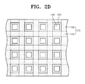
- FIGS. 2A through 2D are plan views of the unit cells of the photo-detector according to an embodiment of the present invention.
- an n + -InP layer 110 on a semi-insulating InP substrate 100, an n + -InP layer 110, an i-InGaAs layer 115, an n-InGaAsP layer 120, an n-InP layer 125, and a p + -InGaAsP layer 130 are sequentially formed.
- the n + -InP layer 110, i-InGaAs layer 115, n-InGaAsP layer 120, n-InP layer 125, and p + -InGaAsP layer 130 may be sequentially formed and crystallized by a metal organic chemical vapor deposition (MOCVD) process.
- MOCVD metal organic chemical vapor deposition
- the i-InGaAs layer 115 may use a material having the proportion of i-In 0.53 Ga 0.47 As, and the n-InGaAsP layer 120 may use a material having the proportion of n + -In 0.73 Ga 0.27 As 0.63 P 0.37 with a band gap having a 1.3 ⁇ m cut-off wavelength.
- the p + -InGaAsP layer 130 may use a material having the proportion of p+-In 0.73 Ga 0.27 As 0.63 P 0.37 37 with a band gap having a 1.3 ⁇ m cut-off wavelength which passing the signal light having a 1.5 ⁇ m laser radar transmission wavelength
- the p + -InGaAsP layer 130 is formed as a thin film on the surface of the n-lnP layer 125, and reduces the ohmic resistance between the electrode and the semiconductor.
- an insulating layer pattern 135 is formed on the p + -InGaAsP layer 130 so that a region to be photo-detected is exposed.
- the insulating layer pattern 135 is formed by a known photolithography process and etching process after an insulating layer is vapor-deposited.
- a p + diffusion region 140 is formed in the selectively exposed p + -InGaAsP layer 130 and n-InP layer 125.
- the p + diffusion region 140 may be formed by the following method. For example, a ZnP3 source and a resultant structure (or a crystal specimen) of the substrate are vacuum-sealed in a quartz ampoule. The vacuum-sealed quartz ampoule is electrically heated to 500°C until Zn is spread on the n-InP layer, thereby forming the p + diffusion region 140. As the p + diffusion region 140 is formed, a p-n junction is formed on the n-InP layer 125.
- the p + diffusion region 140 may be arranged in a regular order, for example, a matrix pattern, on the substrate resultant structure, i.e., the P + -InGaAsP layer 135, as shown in FIG. 2A . As the p + diffusion region 140 is formed, a number of unit cells of the photo-detector are formed.
- the insulating layer pattern 135 is removed by using a known process.
- a first photoresist pattern 150 is formed on the resultant structure of the substrate 100.
- a protecting layer 152 may be interposed between the first photoresist pattern 150 and the surface of the resultant structure, i.e., between the first photoresit pattern 150 and the p + -InGaAsP layer 130, thereby protecting the p + -InGaAsP layer 130 and preventing the exfoliation of the first photoresist pattern 150.
- the first photoresist pattern 150 may have a shape of a number of stripes extending in a row direction, as shown in FIG. 2B .
- the first photoresist pattern 150 is disposed to shield all p + diffusion regions 140 positioned in the same row.
- the first photoresist pattern 150 may have a thickness in the range of about 5 to 10 ⁇ m, and the critical dimension of the first photoresist pattern 150 may be greater than the width of the p + diffusion region 140.
- isolation ions for example, Fe-ions
- the isolation ions may be implanted with a high ion implantation energy so that a final transmission depth of the Fe-ions is positioned in the semi-insulating InP substrate 100.
- the first photoresist pattern 150 is removed by using a known process.
- a row-directional isolation region 160 is formed, by activating the isolation ions implanted in the resultant structure of the substrate. Since the ion implantation energy is controlled so that the transmission depth of the isolation ions, i.e., Fe-ions, is positioned in the semi-insulating InP substrate 100, the bottom of the row-directional isolation region 160 is positioned in the semi-insulating InP substrate 100.
- a second photoresist pattern 165 is formed on the resultant structure of the compound semiconductor substrate on which the row-directional isolation region 160 is formed.
- the second photoresist pattern 165 has a shape of a number of stripes extending in a column direction, so as to be perpendicular to the first photoresist pattern 150,
- the second photoresist pattern 165 is disposed to shield all p + diffusion regions 140 positioned at the same column.
- the second photoresist pattern 165 has a thickness in the range of about 5 to 10 ⁇ m, and has a larger width than that of the p + diffusion region 140.
- the isolation ions for example, Fe-ions, are again implanted in the resultant structure of the substrate exposed by the second photoresist pattern 165. Unlike the conditions of the row-directional ion implantation, the final transmission depth of the Fe-ions are set to be positioned in the n + -InP layer 110 formed on the semi-insulating InP substrate 100.
- the second photoresist pattern 165 is removed, by using a known process.
- a column-directional isolation region 168 is formed, by activating the implanted Fe-ions, thereby forming an isolation region 170.
- the p + diffusion regions 140 i.e., the p-n junction diodes are electrically isolated from other adjacent p-n junction diodes, thereby defining each avalanche type unit cell.
- the row-directionally implanted Fe-ions are activated.
- the row-directionally implanted Fe-ions may not be activated after the row-directional ion implantation is completed.
- the row-directionally implanted Fe-ions may be activated, together with the column-directionally implanted Fe-ions after the column-directional ion implantation is completed.
- the isolation region 170 is formed by deeply implanting the ions, thereby causing no trench structure on the surface of the resultant structure of the substrate 100.
- the isolation region 170 positioned at an edge of the substrate 100 is anisotropically etched so as to expose part of the n + -lnP layer 110 where the Fe-ions are not implanted in the column-direction.
- the anisotropic etching may use reactive ion etching.
- An n-type common electrode 175 is formed, by using a known process, on the surface of the n + -InP layer 110 exposed by the anisotropic etching.
- the n-type common electrode 175 may include, for example, a Ti/Pt/Au laminate.
- an insulating layer 180 is formed on the resultant structure of the substrate 100.
- the insulating layer 180 may be a silicon nitride layer and may be formed after the protecting layer 152 is removed.
- a desired portion of the insulating layer 180 is patterned so that the p + -InGaAsP layer 140 is exposed.
- the insulating layer 180 may be etched so that the whole p + -InGaAsP layer 140 is exposed.
- P-type electrodes 185 are formed at both edges of the p + -InGaAsP layer 140 and insulating layer 180.
- the p-type electrodes 185 may use a Ti/Pt/Au laminate and the Ti/Pt/Au laminate may be used by a known lift off method.
- a metal wiring 190 for connecting the p-type electrodes 185 is formed on the insulating layer 180. Since the metal wiring 190 is formed on the planarized insulating layer 180, the metal wiring is not disconnected and the length of the metal wiring 190 is shortened, thereby reducing resistance. Since the structure of the connection line between the cells is simplified, it is possible to manufacture an array device for a two-dimensional avalanche photo-detector for detecting an image signal of a laser radar, in which the integration density, speed and noise characteristic of a photo-detector per pixel unit are high and the manufacturing efficiency thereof is improved.
- the ground power is applied to the n-type electrode 175, and the source voltage is applied to the p-type electrodes 185.
- an isolation layer is formed, by implanting the Fe-ions, so that the p-n junction diodes, the p-type electrodes and the metal wiring are positioned on the same level.
- the length of the metal wiring is shortened and the arrangement of the metal wiring is simplified.
- the p-n junction side is not exposed, thereby reducing the surface leackage current.
- the present invention is not limited to the aforementioned embodiment.
- the column-directional isolation region 168 is formed after the row-directional isolation region 160 is formed.
- the column-directional isolation region 168 is the row-directiorial isolation region 160 may be formed. But, the depth of the ion implantation in any one of the isolation regions must be controlled to be in the conductive n + -InP layer 110.
- the isolation region for isolating the unit cells of the photo-detector array is formed by the Fe-ion implantation region. Without forming a trench, the isolation layer is formed as the implanted region so as to occupy a desired portion of the resultant structure of the substrate, thereby providing the planarized surface of the resultant structure of the substrate. Consequently, the metal wiring is arranged on the Fe ion implanted planarized surface, thereby preventing the disconnection of the metal wiring and further improving the reproducibility of wiring between cells and electrical reliability.
- the spatial photo-signal distortion phenomenon decreases and attachment of the photodiode array to the driving switching circuitry of array type is simplified to have an accurate and high speed characteristic of receiving an image signal.
- the InGaAsP layer is inserted to weaken the electric field applied to the photo-absorbing layer of the i-InGaAs layer 115 included in the photo-detector and to smooth the flow of the generated photocurrent, the tunnelling leakage current is reduced and the photoelectric conversion efficiency is improved. Accordingly, it is possible to manufacture a two-dimensional infrared detector array device, for detecting an image signal of an eye-safe infrared laser radar, which has the accurate and high characteristic of receiving the image signal, due to its excellent operational characteristic for high bias and its improved electrical stability.
Landscapes
- Light Receiving Elements (AREA)
Description
- The present invention relates to a photo-detector array for detecting an image signal of an infrared laser radar and a method of manufacturing the same, and more particularly, to a two-dimensional avalanche photo-detector array having a planarized surface, for detecting an image signal of an eye-safe infrared laser, and a method of manufacturing the same.
- A photo-detector array for detecting an image signal of an eye-safe infrared laser radar having a wavelength band of 1.55µm includes a number of photo-diodes. The discrete photo-detector includes a semi-insulating InP substrate, a n+-InP layer, an n-InGaAs, n-InGaAsP layer, and n-InP layer layer sequentially stacked on the semi-insulating InP substrate. A photo-absorbing layer is formed in the n-InGaAs layer, and photo-diode amplification region is formed on the n-InP layer where the PN junction is formed. The photo-diodes form unit cells of the photo-detector array, respectively.
- The unit cells of the photo-detector must be electrically isolated for the independent electrical access, and a conventional photo-detector uses a trench for this purpose. The trench is a so-called mesa type groove, and is formed by partially etching the layer and the n+-InP layer.
- However, since the unit cells of a conventional photo-detector array are isolated by the trench, metal wiring for connecting p-type electrodes formed on a p+ diffusion region has to be extended over an inner surface of the trench, and thus the path length of the metal wiring becomes long. As a result, signal delay or signal distortion may occur, and the arrangement of the metal wiring may be complicated. Furthermore, since the isolating trench has a deep and narrow shape, the metal wiring in the inner surface of the trench may not be regularly deposited and it may even be disconnected, thereby deteriorating the reproducibility and reliability of a product.
- Furthermore, since the trench is used to isolate devices, a side of the p-n junction is exposed outwardly by the trench, thereby causing leakage current.
- Accordingly, the photo-detector needs an isolation structure in which the metal wirings between discrete photo diode cells are formed over the electrically isolated flat surface made possible with embedded isolation structure using ion implantation into the semiconductor.
-
EP 0 272 372 A1 on which the preamble of claim 1 is based, discloses a monolithic integrated photo-detector comprising at least one p-n photo diode and at least one corresponding amplifier. Particularly, this configuration of the photo-detector electrically separates the photo-diode and the amplifier by a trench and disposes a wiring electrode in the trench which is connected to the n-region. The wiring of the photo-detector is complicated, since the trench used to isolate the devices has a deep and narrow shape, and signal delay or signal distortion occurs due to different path length of the wirings. - The present invention is defined in the independent claims. Advantageous embodiments of the present invention are defined in the dependent claim.
- The present invention provides a photo-detector, in which a metal wiring connecting electrodes of each cells is positioned on a planarized surface, thereby simplifying the metal wiring arrangement.
- The present invention also provides a two-dimensional photo-detector, for example an avalanche amplification type photo-detector, for detecting an image signal, for example an image signal of a laser radar, in which a structure of a connection line between cells is simplified, thereby improving the integration density, speed and noise characteristic of the photo-detector per pixel unit and improving the manufacturing efficiency thereof.
- The present invention also provides a method of manufacturing a photo-detector, in which a resultant structure has a planarized surface, thereby shortening the path length of metal wiring.
- According to an aspect of the present invention there is provided a photodetector with an isolation regionbeing a Fe-impurity region.
- The compound semiconductor substrate may be a semi-insulating InP substrate, and the multi-layer compound semiconductor layer may be a structure in which an n+-lnP layer, an i-lnGaAs layer, an n-lnGaAsP layer, an n-lnP layer and a p+-InGaAsP layer are sequentially stacked.
- The above and other features and advantages of the present invention will become more apparent by describing in detail exemplary embodiments thereof with reference to the attached drawings in which:
-
FIGS. 1A through 1I are cross-sectional views of the respective processes to explain a method of manufacturing an infrared photo-detector according to an embodiment of the present invention; and -
FIGS. 2A through 2D are plan views of unit cells of the photo-detector according to an embodiment of the present invention. - The present invention will now be described more fully with reference to the accompanying drawings, in which preferred embodiments of the invention are shown. These embodiments are provided so that this disclosure will be thorough and complete, and will fully convey the scope of the invention to those skilled in the art. In drawings, the shape of components may be exaggerated for clarity. Like numbers refer to like elements throughout the specification.
-
FIGS. 1A through 1I are cross-sectional views of the respective processes to explain a method of manufacturing an infrared photo-detector according to an embodiment of the present invention; andFIGS. 2A through 2D are plan views of the unit cells of the photo-detector according to an embodiment of the present invention. - As illustrated in
FIG. 1A , on asemi-insulating InP substrate 100, an n+-InP layer 110, an i-InGaAs layer 115, an n-InGaAsP layer 120, an n-InP layer 125, and a p+-InGaAsP layer 130 are sequentially formed. The n+-InP layer 110, i-InGaAslayer 115, n-InGaAsP layer 120, n-InP layer 125, and p+-InGaAsP layer 130 may be sequentially formed and crystallized by a metal organic chemical vapor deposition (MOCVD) process. The i-InGaAslayer 115 may use a material having the proportion of i-In0.53Ga0.47As, and the n-InGaAsP layer 120 may use a material having the proportion of n+-In0.73Ga0.27As0.63P0.37 with a band gap having a 1.3µm cut-off wavelength. The p+-InGaAsP layer 130 may use a material having the proportion of p+-In0.73Ga0.27As0.63P0.37 37 with a band gap having a 1.3µm cut-off wavelength which passing the signal light having a 1.5µm laser radar transmission wavelength The p+-InGaAsP layer 130 is formed as a thin film on the surface of the n-lnP layer 125, and reduces the ohmic resistance between the electrode and the semiconductor. - As illustrated in
FIG. 1B , aninsulating layer pattern 135 is formed on the p+-InGaAsP layer 130 so that a region to be photo-detected is exposed. Theinsulating layer pattern 135 is formed by a known photolithography process and etching process after an insulating layer is vapor-deposited. - A p+ diffusion region 140 is formed in the selectively exposed p+-
InGaAsP layer 130 and n-InP layer 125. The p+ diffusion region 140 may be formed by the following method. For example, a ZnP3 source and a resultant structure (or a crystal specimen) of the substrate are vacuum-sealed in a quartz ampoule. The vacuum-sealed quartz ampoule is electrically heated to 500°C until Zn is spread on the n-InP layer, thereby forming the p+ diffusion region 140. As the p+ diffusion region 140 is formed, a p-n junction is formed on the n-InP layer 125. The photo-detector has a structure in which the photocurrent is generated by the infrared light absorbed through the i-InGaAs photo-absorbinglayer 115 and is avalanche amplified by the p-n junctionA depletion layer 145 is generated in the p-n junction region, that is, the junction interface between the p+ diffusion region 140 and the n=lnP layer 125. - The p+ diffusion region 140 may be arranged in a regular order, for example, a matrix pattern, on the substrate resultant structure, i.e., the P+-
InGaAsP layer 135, as shown inFIG. 2A . As the p+ diffusion region 140 is formed, a number of unit cells of the photo-detector are formed. - As illustrated in
FIG. 1C , theinsulating layer pattern 135 is removed by using a known process. A firstphotoresist pattern 150 is formed on the resultant structure of thesubstrate 100. A protectinglayer 152 may be interposed between the firstphotoresist pattern 150 and the surface of the resultant structure, i.e., between thefirst photoresit pattern 150 and the p+-InGaAsP layer 130, thereby protecting the p+-InGaAsP layer 130 and preventing the exfoliation of the firstphotoresist pattern 150. - The first
photoresist pattern 150 may have a shape of a number of stripes extending in a row direction, as shown inFIG. 2B . The firstphotoresist pattern 150 is disposed to shield all p+ diffusion regions 140 positioned in the same row. Thefirst photoresist pattern 150 may have a thickness in the range of about 5 to 10µm, and the critical dimension of thefirst photoresist pattern 150 may be greater than the width of the p+ diffusion region 140. - In
FIG. 1C , isolation ions, for example, Fe-ions, are implanted in the resultant structure of the substrate exposed by thefirst photoresist pattern 150. The isolation ions may be implanted with a high ion implantation energy so that a final transmission depth of the Fe-ions is positioned in thesemi-insulating InP substrate 100. - As illustrated in
FIG. 1D , thefirst photoresist pattern 150 is removed by using a known process. A row-directional isolation region 160 is formed, by activating the isolation ions implanted in the resultant structure of the substrate. Since the ion implantation energy is controlled so that the transmission depth of the isolation ions, i.e., Fe-ions, is positioned in thesemi-insulating InP substrate 100, the bottom of the row-directional isolation region 160 is positioned in thesemi-insulating InP substrate 100. - As illustrated in
FIGS. 1E and2C , asecond photoresist pattern 165 is formed on the resultant structure of the compound semiconductor substrate on which the row-directional isolation region 160 is formed. Thesecond photoresist pattern 165 has a shape of a number of stripes extending in a column direction, so as to be perpendicular to thefirst photoresist pattern 150, Thesecond photoresist pattern 165 is disposed to shield all p+ diffusion regions 140 positioned at the same column. Like thefirst photoresist pattern 150, thesecond photoresist pattern 165 has a thickness in the range of about 5 to 10µm, and has a larger width than that of the p+ diffusion region 140. The isolation ions, for example, Fe-ions, are again implanted in the resultant structure of the substrate exposed by thesecond photoresist pattern 165. Unlike the conditions of the row-directional ion implantation, the final transmission depth of the Fe-ions are set to be positioned in the n+-InP layer 110 formed on thesemi-insulating InP substrate 100. - As illustrated in
FIGS. 1F and2D , thesecond photoresist pattern 165 is removed, by using a known process. A column-directional isolation region 168 is formed, by activating the implanted Fe-ions, thereby forming anisolation region 170. As theisolation region 170 is formed, the p+ diffusion regions 140, i.e., the p-n junction diodes are electrically isolated from other adjacent p-n junction diodes, thereby defining each avalanche type unit cell. - In the present embodiment, after the row-directional ion implantation is completed, the row-directionally implanted Fe-ions are activated. However, the present invention is not limited to this. The row-directionally implanted Fe-ions may not be activated after the row-directional ion implantation is completed. The row-directionally implanted Fe-ions may be activated, together with the column-directionally implanted Fe-ions after the column-directional ion implantation is completed.
- Unlike a conventional trench structure, the
isolation region 170 according to the present embodiment is formed by deeply implanting the ions, thereby causing no trench structure on the surface of the resultant structure of thesubstrate 100. - As illustrated in
FIG. 1G , theisolation region 170 positioned at an edge of thesubstrate 100 is anisotropically etched so as to expose part of the n+-lnP layer 110 where the Fe-ions are not implanted in the column-direction. The anisotropic etching may use reactive ion etching. An n-typecommon electrode 175 is formed, by using a known process, on the surface of the n+-InP layer 110 exposed by the anisotropic etching. The n-typecommon electrode 175 may include, for example, a Ti/Pt/Au laminate. - As illustrated in
FIG, 1H , an insulatinglayer 180 is formed on the resultant structure of thesubstrate 100. The insulatinglayer 180 may be a silicon nitride layer and may be formed after theprotecting layer 152 is removed. A desired portion of the insulatinglayer 180 is patterned so that the p+-InGaAsP layer 140 is exposed. The insulatinglayer 180 may be etched so that the whole p+-InGaAsP layer 140 is exposed. P-type electrodes 185 are formed at both edges of the p+-InGaAsP layer 140 and insulatinglayer 180. The p-type electrodes 185 may use a Ti/Pt/Au laminate and the Ti/Pt/Au laminate may be used by a known lift off method. - As illustrated in
FIG. 1 ametal wiring 190 for connecting the p-type electrodes 185 is formed on the insulatinglayer 180. Since themetal wiring 190 is formed on the planarized insulatinglayer 180, the metal wiring is not disconnected and the length of themetal wiring 190 is shortened, thereby reducing resistance. Since the structure of the connection line between the cells is simplified, it is possible to manufacture an array device for a two-dimensional avalanche photo-detector for detecting an image signal of a laser radar, in which the integration density, speed and noise characteristic of a photo-detector per pixel unit are high and the manufacturing efficiency thereof is improved. The ground power is applied to the n-type electrode 175, and the source voltage is applied to the p-type electrodes 185. - In the photo-detector according to an embodiment of the present invention, an isolation layer is formed, by implanting the Fe-ions, so that the p-n junction diodes, the p-type electrodes and the metal wiring are positioned on the same level. As a result, the length of the metal wiring is shortened and the arrangement of the metal wiring is simplified. Additionally, since a trench is not formed, the p-n junction side is not exposed, thereby reducing the surface leackage current.
- In a conventional photo-detector, since the p-n junction is formed on an InGaAs layer having a small band gap, a relatively large tunnelling leakage current occurs. However, in the photo-detector of the present embodiment, since the InGaAsP layer is inserted between the n-InP layer and the i-InGaAs layer, the electric field applied to an i-InGaAs layer is weakened, thereby reducing the tunnelling leakage current and improving the durability when the high bias voltage is applied for photocurrent amplification.
- The present invention is not limited to the aforementioned embodiment. In the present embodiment, after the row-
directional isolation region 160 is formed, the column-directional isolation region 168 is formed. However, after the column-directional isolation region 168 is the row-directiorial isolation region 160 may be formed. But, the depth of the ion implantation in any one of the isolation regions must be controlled to be in the conductive n+-InP layer 110. - As described above, according to the present invention, the isolation region for isolating the unit cells of the photo-detector array is formed by the Fe-ion implantation region. Without forming a trench, the isolation layer is formed as the implanted region so as to occupy a desired portion of the resultant structure of the substrate, thereby providing the planarized surface of the resultant structure of the substrate. Consequently, the metal wiring is arranged on the Fe ion implanted planarized surface, thereby preventing the disconnection of the metal wiring and further improving the reproducibility of wiring between cells and electrical reliability.
- Furthermore, since the arrangement of the metal wiring is simplified, the spatial photo-signal distortion phenomenon decreases and attachment of the photodiode array to the driving switching circuitry of array type is simplified to have an accurate and high speed characteristic of receiving an image signal.
- Furthermore, since the p-n junction interface is not exposed, the leakage current is reduced.
- Furthermore, since the InGaAsP layer is inserted to weaken the electric field applied to the photo-absorbing layer of the i-
InGaAs layer 115 included in the photo-detector and to smooth the flow of the generated photocurrent, the tunnelling leakage current is reduced and the photoelectric conversion efficiency is improved. Accordingly, it is possible to manufacture a two-dimensional infrared detector array device, for detecting an image signal of an eye-safe infrared laser radar, which has the accurate and high characteristic of receiving the image signal, due to its excellent operational characteristic for high bias and its improved electrical stability.
Claims (15)
- A photo-detector comprising:a semi-insulating compound semiconductor substrate (100);a multi-layer compound semiconductor layer (110, 115, 120, 125, 130) formed on the semi-insulating compound semiconductor substrate (100);a number of p-n junction diodes (125, 130, 140) arranged in a regular order In a selected region of the multi-layer compound semiconductor layer (110, 115, 120, 125, 130); andisolation regions (160, 168) formed by impurity regions formed in the multi-layer compound semiconductor layer (110, 115, 120, 125, 130), so as to surround each p-n junction diode, for individually electrically isolating the p-n junction diodes,wherein the surface of each isolation region (160, 168) formed on the multi-layer compound semiconductor layer (110, 115, 120, 1,25, 130) is flat,characterized in that
the number of p-n junction diodes are arranged in a two-dimensional matrix pattern of p-n junction diodes in a row-axis direction and p-n junction diodes in a column-axis direction;
the isolation regions (160, 168) are formed as implanted stripes in the row-axis direction and in the column-axis direction;
the transmission depth of implanted impurities of the impurity region of the isolation regions in the row-axis direction (160) is positioned in the semi-insulating compound semiconductor substrate (100) so as to position the bottom of the Isolation regions in the row-axis direction (160) in the semi-insulating compound semiconductor substrate (100), and the transmission depth of implanted impurities of the impurity region of the isolation regions in the column-axis direction (168) is positioned in a conductive semiconductor (110) formed on the semi-insulating compound semiconductor substrate (100) so as to position the bottom of the isolation regions in the column-axis direction (168) in the conductive semiconductor,
wherein the conductive semiconductor is a part of the multi-layer compound semiconductor layer (110, 115, 120, 125, 130) and wherein the conductive semiconductor is the layer of the multi-layer compound semiconductor layer (110, 115, 120, 125, 130) being on the semi-insulating compound semiconductor substrate (100). - The photo-detector of claim 1, wherein the isolation regions (160, 168) are Fe-impurity regions.
- The photo-detector of any of the preceding claims, wherein the semi-insulating compound semiconductor substrate (100) is a semi-insulating InP substrate.
- The photo-detector of claim 3, wherein the multi-layer compound semiconductor layer (110, 115, 120, 125, 130) is a structure formed by sequentially stacking an n+-InP layer (110), an i-InGaAs layer (115), an n-InGaAsP layer (120), an n-InP layer (125), and a p*-InGaAsP layer (130).
- The photo-detector of claim 4, wherein the p-n junction diodes include a p+ diffusion region (140) formed at a desired portion in the n-InP layer (125) and the p+-InGaAsP layer (130).
- The photo-detector of claim 5 with a region of the n+-InP layer (110), wherein part of the n+-InP layer (110) of a predetermined thickness without the isolation regions (160, 168) exists at an edge of the semi-insulating compound semiconductor substrate (100);
a n-type electrode (175) is further formed on said region of the n+-InP layer (110) on the n+-InP layer (110) at the edge of the semi-insulating compound semiconductor substrate (100); and
p-type electrodes (185) on the p+ diffusion layer (140) are further formed at an edge of the p+ diffusion layer (140). - The photo-detector of claim 6, wherein metal wiring (190) is further formed to connect the p-type electrodes (185).
- A method of manufacturing a photo-detector comprising:providing a semi-insulating compound semiconductor substrate (100);forming a multi-layer compound semiconductor layer (110, 115, 120, 125, 130) on the semi-insulating compound semiconductor substrate (100);forming a number of p-n junction diodes (125, 130, 140) at a desired portion of the multi-layer compound semiconductor layer (110, 115, 120, 125, 130); andforming isolation regions (160, 168) by implanting impurities so as to surround each p-n junction diode and to individually electrically isolate the p-n junction diodes,wherein the surface of each isolation region (160, 168) formed on the multi-layer compound semiconductor layer (110, 115, 120, 125, 130) is flat,characterized in that
the number of p-n junction diodes are arranged in a two-dimensional matrix pattern of p-n junction diodes in a row-axis direction and p-n junction diodes in a column-axis direction;
the isolation regions (160, 168) are formed as implanted stripes in the row-axis direction and in the column-axis direction;
the transmission depth of the implanted impurities of the isolation regions in the row-axis direction (160) is positioned in the semi-insulating compound semiconductor substrate (100) so as to position the bottom of the isolation regions In the row-axis direction (160) in the semi-insulating compound semiconductor substrate (100), and the transmission depth of the implanted impurities of the isolation regions in the column-axis direction (168) is positioned in a conductive semiconductor (110) formed on the semi-insulating compound semiconductor substrate (100) so as to position the bottom of the isolation regions in the column-axis direction (168) in the conductive semiconductor,
wherein the conductive semiconductor is a part of the multi-layer compound semiconductor layer (110, 115, 120, 125, 130) and wherein the conductive semiconductor is the layer of the multi-layer compound semiconductor layer (110, 115, 120, 125, 130) being on the semi-insulating compound semiconductor substrate (100). - The method of claim 8, wherein the semi-insulating compound semiconductor substrate (100) is a semi-insulating InP substrate.
- The method of claim 9, wherein the forming of the multi-layer compound semiconductor layer (110, 115, 120, 125, 130) comprises:forming an n+-InP layer (110) on the semi-insulating compound semiconductor substrate (100);forming an i-InGaAs layer (115) on the n+-InP layer (110);forming an n-InGaAsP layer (120) on the i-InGaAs layer (115);forming an n-InP layer (125) on the n-InGaAsP layer (120); andforming a p+-InGaAsP layer (130) on the n-InP layer (125).
- The method of claim 10, wherein the forming of the p-n junction diodes comprises:forming a mask pattern on the p+-InGaAsP layer (130), so that a desired region of the p+-InGaAsP layer (130) is exposed;forming a p+ diffusion layer (140) in the n-InP layer (125) and the p+-InGaAsP layer (130), by diffusing p-type impurities in the exposed region; andremoving the mask pattern.
- The method of claim 11, wherein the p-type impurities are Zn.
- The method of claim 10, after the forming of the isolation regions (160, 168), further comprising:etching the p+-InGaAsP layer (130), p+-InP layer, the n-InP layer (125), the n-InGaAsP layer (120) and the i-InGaAs layer (115), so that the n+-InP layer (110) formed at an edge of the semi-insufating compound semiconductor substrate (100) is exposed;forming an n-type electrode (175) on a selected region of the n+-InP layer (110) on the n+InP layer at the edge of the semi-insulating compound semiconductor substrate (100);forming p-type electrodes (185) at an edge of the p+ diffusion layer (140); andforming metal wiring for connecting the p-type electrodes (185).
- The method of any of claims 8 to 13, wherein the forming of the isolation regions (160, 168) is carried out, by implanting impurity ions surrounding each p-n junction diode.
- The method of claim 14, wherein the forming of the isolation regions (160, 168) comprises:forming a first photoresist pattern (150) for shielding the p-n junction diodes arranged in the row-axis direction;implanting Fe-impurities in the exposed multi-layer compound semiconductor layer (110, 115, 120, 125, 130) so as to form the isolation regions in the row-axis direction (160);removing the first photoresist pattern (150);forming a second photoresist pattern (165) for shielding the p-n junction diodes arranged in the column-axis direction;implanting Fe-impurities in the exposed multi-layer compound semiconductor layer (110, 115, 120, 125, 130) so as to form the isolation regions in the column-axis direction (168); andactivating the ion-implanted Fe-impurities.
Applications Claiming Priority (1)
| Application Number | Priority Date | Filing Date | Title |
|---|---|---|---|
| KR1020050121973A KR100670828B1 (en) | 2005-12-12 | 2005-12-12 | Photodetector for detecting image signal of infrared laser radar and manufacturing method thereof |
Publications (2)
| Publication Number | Publication Date |
|---|---|
| EP1796169A1 EP1796169A1 (en) | 2007-06-13 |
| EP1796169B1 true EP1796169B1 (en) | 2012-03-21 |
Family
ID=37888089
Family Applications (1)
| Application Number | Title | Priority Date | Filing Date |
|---|---|---|---|
| EP06125646A Expired - Fee Related EP1796169B1 (en) | 2005-12-12 | 2006-12-07 | Infrared-Photo-detector array with implanted electrical isolation of neigboring detector elements and method of manufacturing the same |
Country Status (3)
| Country | Link |
|---|---|
| US (2) | US7541659B1 (en) |
| EP (1) | EP1796169B1 (en) |
| KR (1) | KR100670828B1 (en) |
Families Citing this family (11)
| Publication number | Priority date | Publication date | Assignee | Title |
|---|---|---|---|---|
| JP2010223715A (en) * | 2009-03-23 | 2010-10-07 | Shiro Sakai | Photodetector and spectrum detector |
| EP2474034B1 (en) * | 2009-08-31 | 2014-11-12 | Intevac, Inc. | Low energy portable low-light camera with wavelength cutoff |
| WO2011050322A1 (en) * | 2009-10-23 | 2011-04-28 | Lockheed Martin Corporation | Barrier photodetector with planar top layer |
| US8330171B2 (en) | 2010-07-23 | 2012-12-11 | Intel Corporation | High speed, wide optical bandwidth, and high efficiency resonant cavity enhanced photo-detector |
| US9653507B2 (en) | 2014-06-25 | 2017-05-16 | Taiwan Semiconductor Manufacturing Co., Ltd. | Deep trench isolation shrinkage method for enhanced device performance |
| US9871067B2 (en) * | 2015-11-17 | 2018-01-16 | Taiwan Semiconductor Manufacturing Co., Ltd. | Infrared image sensor component |
| US10211750B2 (en) | 2016-02-12 | 2019-02-19 | Schneider Electric It Corporation | Apparatus and method for low frequency power inverter |
| CN107706263B (en) * | 2017-10-30 | 2020-07-07 | 浙江大学 | Double-color detector and preparation method thereof |
| CN108257986A (en) * | 2018-01-18 | 2018-07-06 | 中国电子科技集团公司第四十四研究所 | Plane AlGaN ultraviolet detector array structures and preparation method thereof |
| CN110690235B (en) * | 2019-09-05 | 2022-03-29 | 中国电子科技集团公司第十三研究所 | Detector array chip and preparation method thereof |
| CN112909117B (en) * | 2021-01-22 | 2022-08-02 | 湖北大学 | Silicon-doped cerium element infrared detector, preparation method and system |
Family Cites Families (12)
| Publication number | Priority date | Publication date | Assignee | Title |
|---|---|---|---|---|
| US675321A (en) * | 1900-09-28 | 1901-05-28 | Horace Brownfield | Fish-hook. |
| DE3712864C2 (en) * | 1986-09-01 | 2001-05-17 | Daimler Chrysler Ag | Monolithically integrated photo receiver |
| DE3629681A1 (en) * | 1986-09-01 | 1988-03-10 | Licentia Gmbh | PHOTO RECEIVER |
| DE3644408A1 (en) * | 1986-12-24 | 1988-07-07 | Licentia Gmbh | PHOTO RECEIVER |
| US5086004A (en) * | 1988-03-14 | 1992-02-04 | Polaroid Corporation | Isolation of layered P-N junctions by diffusion to semi-insulating substrate and implantation of top layer |
| DE3908886A1 (en) * | 1989-03-17 | 1990-09-20 | Siemens Ag | DOUBLE PIN PHOTODIOD WITH LOCKING P-N TRANSITION BETWEEN SUBSTRATE AND ABSORPTION LAYER |
| US6051857A (en) * | 1998-01-07 | 2000-04-18 | Innovision, Inc. | Solid-state imaging device and method of detecting optical signals using the same |
| KR100298573B1 (en) * | 1998-03-30 | 2001-10-27 | 김충환 | Triac device of planar type |
| CA2355146A1 (en) * | 1999-10-18 | 2001-04-26 | Yasunori Arima | Light-receiving element array and light-receiving element array chip |
| US6870207B2 (en) | 2000-04-24 | 2005-03-22 | The University Of Connecticut | III-V charge coupled device suitable for visible, near and far infra-red detection |
| WO2002007226A1 (en) * | 2000-07-18 | 2002-01-24 | Nippon Sheet Glass Co., Ltd. | Photodetector array |
| US6753214B1 (en) | 2001-02-16 | 2004-06-22 | Optical Communication Products, Inc. | Photodetector with isolation implant region for reduced device capacitance and increased bandwidth |
-
2005
- 2005-12-12 KR KR1020050121973A patent/KR100670828B1/en not_active Expired - Lifetime
-
2006
- 2006-12-07 US US11/635,170 patent/US7541659B1/en not_active Expired - Fee Related
- 2006-12-07 EP EP06125646A patent/EP1796169B1/en not_active Expired - Fee Related
-
2009
- 2009-04-23 US US12/428,575 patent/US7855094B2/en not_active Expired - Fee Related
Also Published As
| Publication number | Publication date |
|---|---|
| US7541659B1 (en) | 2009-06-02 |
| US20090239328A1 (en) | 2009-09-24 |
| US20090140291A1 (en) | 2009-06-04 |
| US7855094B2 (en) | 2010-12-21 |
| EP1796169A1 (en) | 2007-06-13 |
| KR100670828B1 (en) | 2007-01-19 |
Similar Documents
| Publication | Publication Date | Title |
|---|---|---|
| US7855094B2 (en) | Photo-detector for detecting image signal of infrared laser radar and method of manufacturing the same | |
| EP1636856B1 (en) | Ultra thin back-illuminated photodiode array structures and fabrication methods | |
| US8441032B2 (en) | Low-level signal detection by semiconductor avalanche amplification | |
| US20080121866A1 (en) | Avalanche photodiode detector | |
| JP2005259829A (en) | Back-illuminated light receiving element array | |
| US5185272A (en) | Method of producing semiconductor device having light receiving element with capacitance | |
| EP0452801B1 (en) | Semiconductor device having light receiving element and method of producing the same | |
| KR20080100473A (en) | Photodiode having increased proportion of light-sensitive area to ligth-insensitive area | |
| KR20130069127A (en) | Avalanche photo diode and manufacturing method of the same | |
| US7560791B2 (en) | Front lit PIN/NIP diode having a continuous anode/cathode | |
| EP1182705A1 (en) | Light-receiving element array and light-receiving element array chip | |
| US6495380B2 (en) | Epitaxially grown avalanche photodiode | |
| US8999744B2 (en) | Avalanche photodiodes and methods of fabricating the same | |
| WO2020104220A1 (en) | Multi-junction pico-avalanche detector | |
| US10658538B2 (en) | Optical detection device | |
| US20060189027A1 (en) | Method of fabricating avalanche photodiode | |
| JP4109159B2 (en) | Semiconductor photo detector | |
| US4301463A (en) | Demultiplexing photodetector | |
| US12628464B2 (en) | Systems and methods for stacked sensors with electrical insulation | |
| JP2002319669A (en) | Back-illuminated photodiode and photodiode array | |
| US20180254300A1 (en) | Photodiode matrix with isolated cathodes | |
| CN116845120B (en) | A single-photon avalanche diode unit, detector and its fabrication method | |
| KR20170072681A (en) | Low dark-current avalanche photodiode | |
| JPH05102517A (en) | Avalanche photodiode and manufacturing method thereof | |
| US20230042681A1 (en) | Spad pixel for a backside illuminated image sensor |
Legal Events
| Date | Code | Title | Description |
|---|---|---|---|
| PUAI | Public reference made under article 153(3) epc to a published international application that has entered the european phase |
Free format text: ORIGINAL CODE: 0009012 |
|
| AK | Designated contracting states |
Kind code of ref document: A1 Designated state(s): AT BE BG CH CY CZ DE DK EE ES FI FR GB GR HU IE IS IT LI LT LU LV MC NL PL PT RO SE SI SK TR |
|
| AX | Request for extension of the european patent |
Extension state: AL BA HR MK YU |
|
| RIN1 | Information on inventor provided before grant (corrected) |
Inventor name: KIM, BO WOO Inventor name: KIM, HO YOUNG Inventor name: KIM, YONG WON Inventor name: OH, MYOUNG SOOK Inventor name: HONG, SEON EUI Inventor name: NAM, EUN SOO |
|
| 17P | Request for examination filed |
Effective date: 20071212 |
|
| AKX | Designation fees paid |
Designated state(s): DE FR |
|
| 17Q | First examination report despatched |
Effective date: 20080131 |
|
| GRAP | Despatch of communication of intention to grant a patent |
Free format text: ORIGINAL CODE: EPIDOSNIGR1 |
|
| GRAS | Grant fee paid |
Free format text: ORIGINAL CODE: EPIDOSNIGR3 |
|
| GRAA | (expected) grant |
Free format text: ORIGINAL CODE: 0009210 |
|
| AK | Designated contracting states |
Kind code of ref document: B1 Designated state(s): DE FR |
|
| REG | Reference to a national code |
Ref country code: DE Ref legal event code: R096 Ref document number: 602006028286 Country of ref document: DE Effective date: 20120516 |
|
| PLBE | No opposition filed within time limit |
Free format text: ORIGINAL CODE: 0009261 |
|
| STAA | Information on the status of an ep patent application or granted ep patent |
Free format text: STATUS: NO OPPOSITION FILED WITHIN TIME LIMIT |
|
| PGFP | Annual fee paid to national office [announced via postgrant information from national office to epo] |
Ref country code: DE Payment date: 20121121 Year of fee payment: 7 |
|
| 26N | No opposition filed |
Effective date: 20130102 |
|
| REG | Reference to a national code |
Ref country code: DE Ref legal event code: R097 Ref document number: 602006028286 Country of ref document: DE Effective date: 20130102 |
|
| REG | Reference to a national code |
Ref country code: FR Ref legal event code: ST Effective date: 20130830 |
|
| PG25 | Lapsed in a contracting state [announced via postgrant information from national office to epo] |
Ref country code: FR Free format text: LAPSE BECAUSE OF NON-PAYMENT OF DUE FEES Effective date: 20130102 |
|
| REG | Reference to a national code |
Ref country code: DE Ref legal event code: R119 Ref document number: 602006028286 Country of ref document: DE |
|
| REG | Reference to a national code |
Ref country code: DE Ref legal event code: R119 Ref document number: 602006028286 Country of ref document: DE Effective date: 20140701 |
|
| PG25 | Lapsed in a contracting state [announced via postgrant information from national office to epo] |
Ref country code: DE Free format text: LAPSE BECAUSE OF NON-PAYMENT OF DUE FEES Effective date: 20140701 |