EP1796150B1 - Method for algan vapor-phase growth - Google Patents
Method for algan vapor-phase growth Download PDFInfo
- Publication number
- EP1796150B1 EP1796150B1 EP05781000.4A EP05781000A EP1796150B1 EP 1796150 B1 EP1796150 B1 EP 1796150B1 EP 05781000 A EP05781000 A EP 05781000A EP 1796150 B1 EP1796150 B1 EP 1796150B1
- Authority
- EP
- European Patent Office
- Prior art keywords
- crystal
- growth
- supply portion
- carrier gas
- gas
- Prior art date
- Legal status (The legal status is an assumption and is not a legal conclusion. Google has not performed a legal analysis and makes no representation as to the accuracy of the status listed.)
- Expired - Lifetime
Links
Images


Classifications
-
- H—ELECTRICITY
- H10—SEMICONDUCTOR DEVICES; ELECTRIC SOLID-STATE DEVICES NOT OTHERWISE PROVIDED FOR
- H10P—GENERIC PROCESSES OR APPARATUS FOR THE MANUFACTURE OR TREATMENT OF DEVICES COVERED BY CLASS H10
- H10P14/00—Formation of materials, e.g. in the shape of layers or pillars
- H10P14/20—Formation of materials, e.g. in the shape of layers or pillars of semiconductor materials
- H10P14/24—Formation of materials, e.g. in the shape of layers or pillars of semiconductor materials using chemical vapour deposition [CVD]
-
- C—CHEMISTRY; METALLURGY
- C30—CRYSTAL GROWTH
- C30B—SINGLE-CRYSTAL GROWTH; UNIDIRECTIONAL SOLIDIFICATION OF EUTECTIC MATERIAL OR UNIDIRECTIONAL DEMIXING OF EUTECTOID MATERIAL; REFINING BY ZONE-MELTING OF MATERIAL; PRODUCTION OF A HOMOGENEOUS POLYCRYSTALLINE MATERIAL WITH DEFINED STRUCTURE; SINGLE CRYSTALS OR HOMOGENEOUS POLYCRYSTALLINE MATERIAL WITH DEFINED STRUCTURE; AFTER-TREATMENT OF SINGLE CRYSTALS OR A HOMOGENEOUS POLYCRYSTALLINE MATERIAL WITH DEFINED STRUCTURE; APPARATUS THEREFOR
- C30B23/00—Single-crystal growth by condensing evaporated or sublimed materials
- C30B23/002—Controlling or regulating
-
- C—CHEMISTRY; METALLURGY
- C30—CRYSTAL GROWTH
- C30B—SINGLE-CRYSTAL GROWTH; UNIDIRECTIONAL SOLIDIFICATION OF EUTECTIC MATERIAL OR UNIDIRECTIONAL DEMIXING OF EUTECTOID MATERIAL; REFINING BY ZONE-MELTING OF MATERIAL; PRODUCTION OF A HOMOGENEOUS POLYCRYSTALLINE MATERIAL WITH DEFINED STRUCTURE; SINGLE CRYSTALS OR HOMOGENEOUS POLYCRYSTALLINE MATERIAL WITH DEFINED STRUCTURE; AFTER-TREATMENT OF SINGLE CRYSTALS OR A HOMOGENEOUS POLYCRYSTALLINE MATERIAL WITH DEFINED STRUCTURE; APPARATUS THEREFOR
- C30B25/00—Single-crystal growth by chemical reaction of reactive gases, e.g. chemical vapour-deposition growth
- C30B25/02—Epitaxial-layer growth
-
- C—CHEMISTRY; METALLURGY
- C30—CRYSTAL GROWTH
- C30B—SINGLE-CRYSTAL GROWTH; UNIDIRECTIONAL SOLIDIFICATION OF EUTECTIC MATERIAL OR UNIDIRECTIONAL DEMIXING OF EUTECTOID MATERIAL; REFINING BY ZONE-MELTING OF MATERIAL; PRODUCTION OF A HOMOGENEOUS POLYCRYSTALLINE MATERIAL WITH DEFINED STRUCTURE; SINGLE CRYSTALS OR HOMOGENEOUS POLYCRYSTALLINE MATERIAL WITH DEFINED STRUCTURE; AFTER-TREATMENT OF SINGLE CRYSTALS OR A HOMOGENEOUS POLYCRYSTALLINE MATERIAL WITH DEFINED STRUCTURE; APPARATUS THEREFOR
- C30B29/00—Single crystals or homogeneous polycrystalline material with defined structure characterised by the material or by their shape
- C30B29/10—Inorganic compounds or compositions
- C30B29/40—AIIIBV compounds wherein A is B, Al, Ga, In or Tl and B is N, P, As, Sb or Bi
- C30B29/403—AIII-nitrides
-
- H—ELECTRICITY
- H10—SEMICONDUCTOR DEVICES; ELECTRIC SOLID-STATE DEVICES NOT OTHERWISE PROVIDED FOR
- H10P—GENERIC PROCESSES OR APPARATUS FOR THE MANUFACTURE OR TREATMENT OF DEVICES COVERED BY CLASS H10
- H10P14/00—Formation of materials, e.g. in the shape of layers or pillars
- H10P14/20—Formation of materials, e.g. in the shape of layers or pillars of semiconductor materials
- H10P14/29—Formation of materials, e.g. in the shape of layers or pillars of semiconductor materials characterised by the substrates
- H10P14/2901—Materials
- H10P14/2921—Materials being crystalline insulating materials
-
- H—ELECTRICITY
- H10—SEMICONDUCTOR DEVICES; ELECTRIC SOLID-STATE DEVICES NOT OTHERWISE PROVIDED FOR
- H10P—GENERIC PROCESSES OR APPARATUS FOR THE MANUFACTURE OR TREATMENT OF DEVICES COVERED BY CLASS H10
- H10P14/00—Formation of materials, e.g. in the shape of layers or pillars
- H10P14/20—Formation of materials, e.g. in the shape of layers or pillars of semiconductor materials
- H10P14/34—Deposited materials, e.g. layers
- H10P14/3402—Deposited materials, e.g. layers characterised by the chemical composition
- H10P14/3414—Deposited materials, e.g. layers characterised by the chemical composition being group IIIA-VIA materials
- H10P14/3416—Nitrides
-
- Y—GENERAL TAGGING OF NEW TECHNOLOGICAL DEVELOPMENTS; GENERAL TAGGING OF CROSS-SECTIONAL TECHNOLOGIES SPANNING OVER SEVERAL SECTIONS OF THE IPC; TECHNICAL SUBJECTS COVERED BY FORMER USPC CROSS-REFERENCE ART COLLECTIONS [XRACs] AND DIGESTS
- Y10—TECHNICAL SUBJECTS COVERED BY FORMER USPC
- Y10T—TECHNICAL SUBJECTS COVERED BY FORMER US CLASSIFICATION
- Y10T117/00—Single-crystal, oriented-crystal, and epitaxy growth processes; non-coating apparatus therefor
- Y10T117/10—Apparatus
Definitions
- the present invention relates to epitaxial growth method for AlGaN utilized in an ultraviolet laser, LED, and a high-frequency high-power electronic device.
- HB Horizontal Bridgiman
- LEC Liquid Encapsulated Czochralski
- hetero-epitaxial growth of AlGaN on a substrate for example, sapphire substrate
- HVPE HydroCVD
- a Ga source gas, and an NH 3 source gas are mixed in a mixing portion, and the mixed gas is transported to a growth portion (also called substrate portion because the substrate is located).
- AlGaN is grown on the sapphire substrate accommodated in the growth portion.
- a high growth rate is one of advantages in the HVPE method which is of a quartz reaction tube hot-wall method. Therefore, conventionally the HVPE method is used to produce a high sensitive photo-sensor in which a thick film is required and a power device (particularly, power-supply device in which GaAs is used) in which a thick-film, high-quality crystal is required, and HVPE method is also utilized as a method of producing the substrate, particularly a GaN substrate.
- Patent Document 1 GaN nitride based compound semiconductor crystal growth method (TOYODA GOSEI CO., LTD et al.)" and Patent Document 2 "Epitaxial wafer and production method thereof (Sumitomo Electric Industries, Ltd)" disclose that the HVPE method is utilized for the method of producing the GaN substrate.
- Patent Document 3 Japanese Patent Application No. 2002-106102
- US2003045017 (A1) concerns a method for fabricating a GaN-based III-V Group compound semiconductor that utilizes a regrowth method based on the HVPE method to form a second III-V Group compound semiconductor layer having a flat surface on a first III-V Group compound semiconductor layer formed with a mask layer.
- the method uses a mixed carrier gas of hydrogen gas and nitrogen gas to control formation of a facet group including at least the ⁇ 33-62 ⁇ facet by the regrowth, and conducting the regrowth until a plane parallel to the surface of the first III-V Group compound semiconductor layer is once annihilated.
- US4144116 (A ) relates to a method of manufacturing gallium nitride crystals by reaction of galium halide and ammonia in which free hydrogen chloride is introduced into the reaction and deposition zones.
- US6265287 (B1) describes a method for growing a compound semiconductor on a substrate held by a susceptor provided in a reaction chamber in accordance with a metalorganic vapor phase epitaxy technique.
- the method includes the steps of: supplying a Group III source gas containing indium and a Group V source gas containing nitrogen into the reaction chamber; and mixing the Group III and Group V source gases, supplied into the reaction chamber, with each other, and supplying a rare gas as a carrier gas into the reaction chamber so as to carry the mixed source gas onto the upper surface of the substrate.
- US6440823 (B1) describes a low defect density (Ga, Al, In) N material.
- the (Ga, Al, In) N material may be of large area, crack-free character, having a defect density as low as 3x10⁶ defects/cm 2 or lower.
- an HVPE reactor includes one or more gas inlet tubes adjacent to the growth zone, thus allowing fine control of the delivery of reactive gases to the substrate surface.
- an HVPE reactor includes both a growth zone and a growth interruption zone.
- an HVPE reactor includes a slow growth rate gallium source, thus allowing thin layers to be grown.
- Using the slow growth rate gallium source in conjunction with a conventional gallium source allows a device structure to be fabricated during a single furnace run that includes both thick layers (i.e., utilizing the conventional gallium source) and thin layers (i.e., utilizing the slow growth rate gallium source) .
- A. Koukitu et al. Jpn. J. Appl. Phys. 35 (1996) pp. L1638-L1640 ) describes a chemical equilibrium model applied to analyze the growth of AlGaN, InGaN and InAIN alloys using metalorganic vapor-phase epitaxy (MOVPE). The vapor-solid distribution relationship and the phase diagram for deposition are calculated. It is shown that unstable regions of solid composition exist in InGaN and InAIN alloys. The origin of the unstable region is also discussed.
- MOVPE metalorganic vapor-phase epitaxy
- JP2000223418 (A ) relates to a thin GaN layer that is grown at a growth rate of, for example, 4 ⁇ m/h or under by depressurized hydride VPE method on a substrate, and then a thick AlGaN layer is grown enough at a growth rate of 4-400 ⁇ m/h by normal pressure hydride VPE method on this GaN layer.
- the gas-phase epitaxial growth method which grows a second semiconductor layer in thickness d3 at growth rate V3 and growth pressure P3 as it is after growing the first semiconductor layer in thickness d2 at growth rate V2 and growth pressure P2 on the substrate, it is so arranged as to fulfill the conditions of V2 ⁇ V3, and besides P2 ⁇ P3, and besides d2 ⁇ d3.
- WO 2003/085711 & EP1494269 A1 disclose a vapour phase growth method for an Al-containing III-V group compound using AlCl3 and GaCl source gases.
- the inventors study the AlGaN crystal growth by the HVPE method.
- AlGaN is a so-called mixed crystal (sometimes called solid solution) of AlN and GaN
- AlGaN is frequently described as Al x Ga 1-x N to clearly specify a ratio thereof.
- x is a ratio of AlN in the crystal, and x can range from 0 or more to 1 or less.
- Atomic level bonding is established in Al x Ga 1-x N for all the values ranging from 0 to 1, and so-called solid solution is formed.
- AlGaN is AlN. It is necessary to correctly determine the value of x according to application of AlGaN.
- the crystal growth is experimentally performed by changing conditions in various ways.
- an object of the invention is to provide an epitaxial growth method in which the high-quality AlGaN crystal can be grown on the sapphire substrate or the Si substrate by the HVPE method.
- Another object of the invention is to realize a method, in which the value of x of Al x Ga 1-x N can be set at the desired value.
- the inventors find the condition that the linear relationship holds between the source gas ratio and the value of x of the grown Al x Ga 1-x N, and the inventors develop the following crystal growth method in which the value of x of the grown Al x Ga 1-x N can easily be controlled by growing the Al x Ga 1-x N crystal under such conditions.
- the Al composition ratio (x) in the Al x Ga 1-x N crystal is easily set to the desired value.
- the AlGaN crystal having the desired composition ratio can easily be obtained, and a thick-film substrate can be produced.
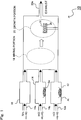
- Fig. 1 is a schematic view showing a vapor phase growth apparatus 10 used in the embodiment.
- the vapor phase growth apparatus 10 for the HVPE (Hydride Vapor Phase Epitaxy) method, used in the embodiment, will be described with reference to Fig. 1 .
- the vapor phase growth apparatus 10 includes an aluminum material supply portion 12 which supplies an aluminum material, a gallium material supply portion 14 which supplies a gallium material, and a nitrogen material supply portion 16 which supplies a nitrogen material.
- the gases supplied from the supply portions are mixed in a mixing portion 18, and the mixed gas is used for the crystal growth in a growth portion 20.
- the growth portion 20 is formed by a quartz reaction chamber, and the growth portion 20 includes an exhaust port 20a.
- the aluminum material supply portion 12 is a predetermined reaction chamber in which metallic aluminum is accommodated.
- a first gas introduction passage 12a is provided in the aluminum material supply portion 12.
- HCl, a hydrogen gas H 2 , and a (inert) carrier gas (IG) are introduced through the first gas introduction passage 12a.
- the metallic aluminum reacts with these gases to generate AlCl 3 which is of the aluminum material source for AlGaN (growth).
- a reaction formula for producing AlCl 3 is expressed as follows. [Chemical formula 1] Al+3HCl ⁇ AlCl 3 +3/2H 2
- AlCl 3 obtained by the chemical formula 1 is transported to the mixing portion 18 along with the carrier gas.
- a hydrogen partial pressure in the carrier gas used is within a predetermined range. Setting the hydrogen partial pressure at a value within the predetermined range facilitates setting a value of x which is of a composition of finally-produced Al x Ga 1-x N at a desired value.
- the specific value of the hydrogen partial pressure will be described later.
- the aluminum material supply portion 12 is kept at a predetermined temperature using a heater (not shown) . Specifically, it is preferable that the aluminum material supply portion 12 be kept at a temperature range (750 °C or less) in which AlCl 3 is generated rather than another substance (AlCl) by the reaction between Al metal and HCl. In the embodiment, the aluminum material supply portion 12 is kept at the temperature of 500 °C.
- AlCl 3 is produced as described above in the embodiment, AlCl 3 powders may be sublimated and transported to the mixing portion 18.
- the gallium material supply portion 14 is a predetermined reaction chamber in which metallic gallium is accommodated.
- a second gas introduction passage 14a is provided in the gallium material supply portion 14.
- HCl, the hydrogen gas H 2 , and the (inert) carrier gas (IG) are introduced through the second gas introduction passage 14a.
- the metallic gallium reacts with these gases to generate GaCl which is of the gallium material for AlGaN (growth) .
- a reaction formula for producing GaCl is expressed as follows. [Chemical Formula 2] Ga+HCl ⁇ GaCl+1/2H 2
- GaCl obtained by the chemical formula 2 is transported to the mixing portion 18 along with the carrier gas.
- the feature of the embodiment is that the hydrogen partial pressure in the carrier gas used is within a predetermined range. Setting the hydrogen partial pressure at a value within the predetermined range facilitates setting a value of x which is of a composition of finally-produced Al x Ga 1-x N at a desired value.
- the specific value of the hydrogen partial pressure will be described later.
- the nitrogen material supply portion 16 is a predetermined reaction chamber as shown in Fig. 1 .
- a third gas introduction passage 16a is provided in the nitrogen material supply portion 16.
- the hydrogen gas H 2 , the (inert) carrier gas (IG), and ammonia NH 3 are introduced through the third gas introduction passage 16a.
- a heater is provided around the nitrogen material supply portion 16 to heat the nitrogen material supply portion 16 at a predetermined temperature.
- the ammonia NH 3 is decomposed at a predetermined ratio in the nitrogen material supply portion 16 by the heat generated by the heater.
- the mixed gas of the ammonia NH 3 decomposed at the predetermined ratio, the hydrogen gas H 2 , and the (inert) carrier gas (IG) are transported to the mixing portion 18.
- setting a hydrogen partial pressure in the carrier gas (F 0 ) at a value within the predetermined range facilitates setting a value of x which is of a composition ratio of Al at a desired value.
- the source gases supplied from the aluminum material supply portion 12, the gallium material supply portion 14, and the nitrogen material supply portion 16 are mixed together in the mixing portion 18.
- a heater (not shown) is provided in the mixing portion 18 to keep the mixing portion 18 at a predetermined temperature.
- a substrate crystal 22 on which the (Al x Ga 1-x N) crystal is grown is accommodated in the growth portion 20.
- a predetermined heater (not shown) is provided to keep the growth portion 20 at a temperature suitable for the crystal growth.
- Various known configurations can be adopted in such heaters. For example, a heater with heating wire and a high-frequency (induction) heater can be used.
- the high-frequency (induction) heater is used to heat the substrate crystal 22 in a concentrated manner.
- optical heating is used to heat the substrate crystal 22 in a concentrated manner.
- a sapphire substrate is used as the substrate crystal 22.
- the substrate crystal 22 is placed on a carbon susceptor 24.
- a device to facilitate setting the value of x in Al x Ga 1-x N is made in the embodiment.
- a ratio of the aluminum material to the gallium material is increased to increase the value of x, and the ratio of the aluminum material to the gallium material is decreased to decrease the value of x.
- the feature of the embodiment is that the linear relationship between "material ratio" and the value of x is established as much as possible by setting the hydrogen partial pressure in the carrier gas at a value with in the desired range.
- the linear relationship can be established as much as possible between the change in material ratio and the change in value of x, which facilitates the adjustment of the value of x.
- the aluminum material supply portion 12 is kept at the temperature of 500 °C, which allows the generation of AlCl to be suppressed to generate the large amount of AlCl 3 . As a result, there is no risk of quartz corrosion even if the reaction chamber is made of the quartz.
- the gallium material supply portion 14 is kept at the temperature of 700 °C using the heater (not shown) .
- the nitrogen material supply portion 16 is also kept at a predetermined temperature using the heater (not shown) .
- the nitrogen material supply portion 16 may be set at the same temperature as the aluminum material supply portion 12, or nitrogen material supply portion 16 may be set at a different temperature.
- the mixing portion 18 is kept at a temperature in which the AlCl 3 generated in the aluminum material supply portion 12 is not deposited in the quartz chamber and at a temperature range in which AlN and GaN are not deposited in the mixing portion 18. This is because the materials can be transported to the growth portion 20 without depositing the material in mid-flow by keeping the mixing portion 18 at the above temperature range.
- the mixing portion is kept at the temperature range of 160 °C or more to 750 °C or less.
- the heater (not shown) is provided around the mixing portion 18 to keep the mixing portion 18 at the above temperature range.
- the substrate crystal is set at a predetermined temperature in the temperature range of 900 °C to 1600 °C. In the embodiment, the substrate crystal in the growth portion 20 is kept at the temperature of 1000 °C.
- Heating the substrate crystal 22 in the collective manner prevents the deposition of AlN or GaN before the AlN or GaN reaches the substrate crystal 22, and the crystal can efficiently be grown on the substrate crystal 22.
- the high-frequency (induction) heating is adopted in the embodiment, another heating method (such as optical heating and resistance heating) may be adopted in place of the high-frequency (induction) heating.
- a resistance wire is provided sufficiently near the substrate crystal 22, which allows the gas not to be heated too much while the substrate crystal 22 is mainly heated.
- the optical heating it is also preferable to adopt a configuration in which a surface of the substrate crystal 22 is irradiated with light from the outside of the quartz reaction chamber. According to the above configuration, the temperature of the substrate crystal 22 can mainly be raised without substantially raising the temperatures of the translucent quartz and the ambient gases.
- the furnace with the light irradiation is known, and the furnace with a light source such as a halogen lamp and a xenon lamp is already brought into practical use.
- Another support material may be used in place of the carbon susceptor 24.
- a Si crystal can also be used as the substrate crystal 22.
- the sapphire substrate is placed on a thin carbon plate and the sapphire substrate is heated by irradiating the sapphire substrate with the light from the carbon plate side.
- the thin carbon plate is placed in the backside of the sapphire substrate, and the sapphire substrate can be heated through the thin carbon plate by irradiating the sapphire substrate with the light from the carbon plate.
- the thick AlGaN substrate can be obtained by removing the sapphire substrate or the Si substrate which is used as the initial substrate.
- the gas in which a predetermined amount of H 2 is mixed in an inert gas such as N 2 , He and Ar is used as the carrier gas in the embodiment.
- the feature in the embodiment is that the further linear relationship between the ratio of aluminum material and gallium material and the ratio of aluminum and gallium in the generated crystal can be established by setting a H 2 concentration in the carrier gas at the later-mentioned range. As a result, compared with the conventional technique, it is easy that the material ratio in the generated crystal is set at the desired ratio.
- the inventors grew the Al x Ga 1-x N thick-film crystal on the substrate crystal 22 (sapphire substrate) by performing the crystal growth of Al x Ga 1-x N for one to ten hours at the above temperature range, and the inventors performed experiments to measure the composition of the obtained Al x Ga 1-x N crystal.
- a value of a vapor phase supply ratio R ([AlCl 3 ]/ ⁇ [AlCl 3 ]+[GaCl] ⁇ ) is changed to grow the Al x Ga 1-x N crystal, and the obtained Al x Ga 1-x N crystal is checked with XRD (X-ray diffraction analysis apparatus) .
- a vertical axis indicates (diffraction) intensity (arbitrary unit) and a horizontal axis indicates an angle (2 ⁇ (degree)).
- the vapor phase supply ratio R When the vapor phase supply ratio R is zero, it means that the aluminum source gas is absent. From the diffraction pattern (solid line in the graph) of the obtained crystal, it is found that the crystal is formed only by GaN.
- the vapor phase supply ratio R is 0.25, it means that the aluminum material ratio is 0.25. From a peak position in the diffraction pattern (dashed line in the graph) of the obtained crystal, it is found that the crystal is the mixed crystal having the composition of Al 0.32 Ga 0.68 N.
- the vapor phase supply ratio R is 0.50, it means that the aluminum material ratio is 0.5. From a peak position in the diffraction pattern (alternate long and short dash line in the graph) of the obtained crystal, it is found that the crystal is the mixed crystal having the composition of Al 0.54 Ga 0.46 N.
- the vertical axis indicates the solid-phase composition ratio x and the horizontal axis indicates the vapor phase supply ratio R.
- the solid-phase composition ratio x is relatively largely changed as the vapor phase supply ratio R is changed.
- the change in solid-phase composition ratio x becomes relatively small even if the vapor phase supply ratio R is changed, and the nonlinearity is exhibited.
- the graph exhibits the remarkable nonlinearity.
- the relationship between the vapor phase supply ratio R and the solid-phase composition ratio x of aluminum becomes the graph which is steeply bent at the value R of about 0.05.
- the solid phase composition ratio x is controlled by adjusting the vapor phase supply ratio R.
- the solid-phase composition ratio x is adjusted at a predetermined value between 0.0 and 0.8.
- the hydrogen partial pressure according to claim 1 it set to more than 0.
- the hydrogen partial pressure according to claim 1 is less than 0.1.
- the further linear relationship can be established between the vapor phase supply ratio R and the solid-phase composition ratio x of the generated crystal by setting the value F 0 of the hydrogen partial pressure in the carrier gas to the predetermined range and setting the process conditions as specified in claim 1.
- the solid phase composition ratio x of the grown crystal can more easily be set at the desired value compared with the conventional technique.
Landscapes
- Chemical & Material Sciences (AREA)
- Engineering & Computer Science (AREA)
- Crystallography & Structural Chemistry (AREA)
- Materials Engineering (AREA)
- Metallurgy (AREA)
- Organic Chemistry (AREA)
- Chemical Kinetics & Catalysis (AREA)
- General Chemical & Material Sciences (AREA)
- Inorganic Chemistry (AREA)
- Crystals, And After-Treatments Of Crystals (AREA)
- Chemical Vapour Deposition (AREA)
Description
- The present invention relates to epitaxial growth method for AlGaN utilized in an ultraviolet laser, LED, and a high-frequency high-power electronic device.
- Usually an HB (Horizontal Bridgiman) method and an LEC (Liquid Encapsulated Czochralski) method are well known as a method of producing a bulk crystal. However, an AlGaN single crystal is hardly grown by these methods.
- Therefore, recently an attempt of the bulk crystal growth is made by a sublimation method and solution growth at high temperature and high pressure. However, the AlGaN crystal which can be used for large-size substrate crystal is not obtained yet even by such methods.
- Currently, hetero-epitaxial growth of AlGaN on a substrate (for example, sapphire substrate) by an HVPE (Hydride Vapor Phase Epitaxy) method is one of the most promising methods of producing the AlGaN single-crystal substrate. In the method, an Al source gas, a Ga source gas, and an NH3 source gas are mixed in a mixing portion, and the mixed gas is transported to a growth portion (also called substrate portion because the substrate is located). Then, AlGaN is grown on the sapphire substrate accommodated in the growth portion.
- Particularly a high growth rate is one of advantages in the HVPE method which is of a quartz reaction tube hot-wall method. Therefore, conventionally the HVPE method is used to produce a high sensitive photo-sensor in which a thick film is required and a power device (particularly, power-supply device in which GaAs is used) in which a thick-film, high-quality crystal is required, and HVPE method is also utilized as a method of producing the substrate, particularly a GaN substrate.
- For example,
Patent Document 1 "Gallium nitride based compound semiconductor crystal growth method (TOYODA GOSEI CO., LTD et al.)" and Patent Document 2 "Epitaxial wafer and production method thereof (Sumitomo Electric Industries, Ltd)" disclose that the HVPE method is utilized for the method of producing the GaN substrate. - The inventor developed a technique of producing a substrate made of a III-V compound including Al by HVPE (method), and the inventor made another patent application (Japanese Patent Application No.
2002-106102 -
- Patent Document 1: Japanese Patent Laid-Open No.
10-215000 - Patent Document 2: Japanese Patent Laid-Open No.
10-316498 - Patent Document 3: Japanese Patent Laid-Open No.
2003-303774 -
US2003045017 (A1) concerns a method for fabricating a GaN-based III-V Group compound semiconductor that utilizes a regrowth method based on the HVPE method to form a second III-V Group compound semiconductor layer having a flat surface on a first III-V Group compound semiconductor layer formed with a mask layer. The method uses a mixed carrier gas of hydrogen gas and nitrogen gas to control formation of a facet group including at least the {33-62} facet by the regrowth, and conducting the regrowth until a plane parallel to the surface of the first III-V Group compound semiconductor layer is once annihilated. -
US4144116 (A ) relates to a method of manufacturing gallium nitride crystals by reaction of galium halide and ammonia in which free hydrogen chloride is introduced into the reaction and deposition zones. -
US6265287 (B1) describes a method for growing a compound semiconductor on a substrate held by a susceptor provided in a reaction chamber in accordance with a metalorganic vapor phase epitaxy technique. The method includes the steps of: supplying a Group III source gas containing indium and a Group V source gas containing nitrogen into the reaction chamber; and mixing the Group III and Group V source gases, supplied into the reaction chamber, with each other, and supplying a rare gas as a carrier gas into the reaction chamber so as to carry the mixed source gas onto the upper surface of the substrate. -
JP8325094 (A -
US6440823 (B1) describes a low defect density (Ga, Al, In) N material. The (Ga, Al, In) N material may be of large area, crack-free character, having a defect density as low as 3x10⁶ defects/cm2 or lower. -
US2002174833 (A1) describes a method and an apparatus for fabricating thin Group III nitride layers as well as Group III nitride layers. According to one aspect, an HVPE reactor includes one or more gas inlet tubes adjacent to the growth zone, thus allowing fine control of the delivery of reactive gases to the substrate surface. According to another aspect, an HVPE reactor includes both a growth zone and a growth interruption zone. According to another aspect, an HVPE reactor includes a slow growth rate gallium source, thus allowing thin layers to be grown. Using the slow growth rate gallium source in conjunction with a conventional gallium source allows a device structure to be fabricated during a single furnace run that includes both thick layers (i.e., utilizing the conventional gallium source) and thin layers (i.e., utilizing the slow growth rate gallium source) . - A. Koukitu et al. (Jpn. J. Appl. Phys. 35 (1996) pp. L1638-L1640) describes a chemical equilibrium model applied to analyze the growth of AlGaN, InGaN and InAIN alloys using metalorganic vapor-phase epitaxy (MOVPE). The vapor-solid distribution relationship and the phase diagram for deposition are calculated. It is shown that unstable regions of solid composition exist in InGaN and InAIN alloys. The origin of the unstable region is also discussed.
-
JP2000223418 (A -
WO 2003/085711 &EP1494269 A1 disclose a vapour phase growth method for an Al-containing III-V group compound using AlCl3 and GaCl source gases. - The inventors study the AlGaN crystal growth by the HVPE method.
- Consequently, the inventors find a problem that controllability of a composition ratio becomes worsened when AlGaN "thick-film" crystal is grown by the HVPE method.
- The problem will be described below.
- Because AlGaN is a so-called mixed crystal (sometimes called solid solution) of AlN and GaN, AlGaN is frequently described as AlxGa1-xN to clearly specify a ratio thereof. Where x is a ratio of AlN in the crystal, and x can range from 0 or more to 1 or less. Atomic level bonding is established in AlxGa1-xN for all the values ranging from 0 to 1, and so-called solid solution is formed. In the case of x=0, because the composition ratio of AlN is zero, AlGaN is GaN. In the case of x=1, AlGaN is AlN. It is necessary to correctly determine the value of x according to application of AlGaN.
- However, in the case where the AlGaN thick film is produced by the HVPE method, because conventionally there is not known an effective technique of setting the value of x which is of the composition ratio of Al at a desired value, the crystal growth is experimentally performed by changing conditions in various ways.
- In view of the foregoing, an object of the invention is to provide an epitaxial growth method in which the high-quality AlGaN crystal can be grown on the sapphire substrate or the Si substrate by the HVPE method. Another object of the invention is to realize a method, in which the value of x of AlxGa1-xN can be set at the desired value.
- As a result of the earnest study, the inventors find that the control of the value of x becomes difficult in the case when the linear relationship does not hold between the source gas ratio and the value of x of the grown AlxGa1-xN.
- Then, as a result of the further study, the inventors find the condition that the linear relationship holds between the source gas ratio and the value of x of the grown AlxGa1-xN, and the inventors develop the following crystal growth method in which the value of x of the grown AlxGa1-xN can easily be controlled by growing the AlxGa1-xN crystal under such conditions.
- The problem is solved by the features and conditions as specified in
claim 1. - Thus, according to the invention, in growing the AlxGa1-xN crystal, the Al composition ratio (x) in the AlxGa1-xN crystal is easily set to the desired value. As a result, compared with the conventional technique, the AlGaN crystal having the desired composition ratio can easily be obtained, and a thick-film substrate can be produced.
-
-
Fig. 1 is a schematic view showing a vapor phase growth apparatus according to an embodiment; -
Fig. 2 is a X-ray diffraction pattern of a growth layer obtained when an AlxGa1-xN crystal is grown while a vapor phase supply ratio R is changed in the case of a hydrogen partial pressure in the carrier gas, F0=0, and -
Fig. 3 is a graph showing a relationship between the vapor phase supply ratio R and a composition of a grown crystal in the case where hydrogen partial pressure in the carrier gas F0 is 0, 0.01, 0.1, and 1. -
- 10
- vapor phase growth apparatus
- 12
- aluminum material supply portion
- 12a
- first gas introduction passage
- 14
- gallium material supply portion
- 14a
- second gas introduction passage
- 16
- nitrogen material supply portion
- 16a
- third gas introduction passage
- 18
- mixing portion
- 20
- growth portion
- 20a
- exhaust port
- 22
- substrate crystal
- 24
- carbon susceptor
- An AlGaN epitaxial layer growth method according to a preferred embodiment of the invention will be described below in detail with reference to the drawings.
-
Fig. 1 is a schematic view showing a vaporphase growth apparatus 10 used in the embodiment. The vaporphase growth apparatus 10 for the HVPE (Hydride Vapor Phase Epitaxy) method, used in the embodiment, will be described with reference toFig. 1 . - As shown in
Fig. 1 , the vaporphase growth apparatus 10 includes an aluminummaterial supply portion 12 which supplies an aluminum material, a galliummaterial supply portion 14 which supplies a gallium material, and a nitrogenmaterial supply portion 16 which supplies a nitrogen material. The gases supplied from the supply portions are mixed in a mixingportion 18, and the mixed gas is used for the crystal growth in agrowth portion 20. Thegrowth portion 20 is formed by a quartz reaction chamber, and thegrowth portion 20 includes an exhaust port 20a. - As shown in
Fig. 1 , the aluminummaterial supply portion 12 is a predetermined reaction chamber in which metallic aluminum is accommodated. A firstgas introduction passage 12a is provided in the aluminummaterial supply portion 12. HCl, a hydrogen gas H2, and a (inert) carrier gas (IG) are introduced through the firstgas introduction passage 12a. The metallic aluminum reacts with these gases to generate AlCl3 which is of the aluminum material source for AlGaN (growth). A reaction formula for producing AlCl3 is expressed as follows.
[Chemical formula 1] Al+3HCl→AlCl3+3/2H2
- AlCl3 obtained by the
chemical formula 1 is transported to the mixingportion 18 along with the carrier gas. - The feature of the embodiment is that a hydrogen partial pressure in the carrier gas used is within a predetermined range. Setting the hydrogen partial pressure at a value within the predetermined range facilitates setting a value of x which is of a composition of finally-produced AlxGa1-xN at a desired value. The specific value of the hydrogen partial pressure will be described later.
- The aluminum
material supply portion 12 is kept at a predetermined temperature using a heater (not shown) . Specifically, it is preferable that the aluminummaterial supply portion 12 be kept at a temperature range (750 °C or less) in which AlCl3 is generated rather than another substance (AlCl) by the reaction between Al metal and HCl. In the embodiment, the aluminummaterial supply portion 12 is kept at the temperature of 500 °C. - Although the AlCl3 is produced as described above in the embodiment, AlCl3 powders may be sublimated and transported to the mixing
portion 18. - As shown in
Fig. 1 , the galliummaterial supply portion 14 is a predetermined reaction chamber in which metallic gallium is accommodated. A secondgas introduction passage 14a is provided in the galliummaterial supply portion 14. HCl, the hydrogen gas H2, and the (inert) carrier gas (IG) are introduced through the secondgas introduction passage 14a. The metallic gallium reacts with these gases to generate GaCl which is of the gallium material for AlGaN (growth) . A reaction formula for producing GaCl is expressed as follows.
[Chemical Formula 2] Ga+HCl→GaCl+1/2H2
- GaCl obtained by the chemical formula 2 is transported to the mixing
portion 18 along with the carrier gas. - The feature of the embodiment is that the hydrogen partial pressure in the carrier gas used is within a predetermined range. Setting the hydrogen partial pressure at a value within the predetermined range facilitates setting a value of x which is of a composition of finally-produced AlxGa1-xN at a desired value. The specific value of the hydrogen partial pressure will be described later.
- The nitrogen
material supply portion 16 is a predetermined reaction chamber as shown inFig. 1 . A thirdgas introduction passage 16a is provided in the nitrogenmaterial supply portion 16. The hydrogen gas H2, the (inert) carrier gas (IG), and ammonia NH3 are introduced through the thirdgas introduction passage 16a. - Although not shown, a heater is provided around the nitrogen
material supply portion 16 to heat the nitrogenmaterial supply portion 16 at a predetermined temperature. The ammonia NH3 is decomposed at a predetermined ratio in the nitrogenmaterial supply portion 16 by the heat generated by the heater. The mixed gas of the ammonia NH3 decomposed at the predetermined ratio, the hydrogen gas H2, and the (inert) carrier gas (IG) are transported to the mixingportion 18. Similarly, in the nitrogenmaterial supply portion 16, setting a hydrogen partial pressure in the carrier gas (F0) at a value within the predetermined range facilitates setting a value of x which is of a composition ratio of Al at a desired value. - The source gases supplied from the aluminum
material supply portion 12, the galliummaterial supply portion 14, and the nitrogenmaterial supply portion 16 are mixed together in the mixingportion 18. A heater (not shown) is provided in the mixingportion 18 to keep the mixingportion 18 at a predetermined temperature. - A
substrate crystal 22 on which the (AlxGa1-xN) crystal is grown is accommodated in thegrowth portion 20. A predetermined heater (not shown) is provided to keep thegrowth portion 20 at a temperature suitable for the crystal growth. Various known configurations can be adopted in such heaters. For example, a heater with heating wire and a high-frequency (induction) heater can be used. - In the embodiment, the high-frequency (induction) heater is used to heat the
substrate crystal 22 in a concentrated manner. Preferably optical heating is used to heat thesubstrate crystal 22 in a concentrated manner. These heaters are well known. - In the embodiment, a sapphire substrate is used as the
substrate crystal 22. Thesubstrate crystal 22 is placed on acarbon susceptor 24. - The above configuration can grow a solid solution of AlxGa1-xN (0<=x<=1) which is of a mixed crystal of AlN and GaN on the
substrate crystal 22. - A device to facilitate setting the value of x in AlxGa1-xN is made in the embodiment. Qualitatively, a ratio of the aluminum material to the gallium material is increased to increase the value of x, and the ratio of the aluminum material to the gallium material is decreased to decrease the value of x.
- However, because generally a linear relationship does not hold between "material ratio" and the value of x, sometimes adjustment is hardly made.
- The feature of the embodiment is that the linear relationship between "material ratio" and the value of x is established as much as possible by setting the hydrogen partial pressure in the carrier gas at a value with in the desired range. As a result, according to the embodiment, the linear relationship can be established as much as possible between the change in material ratio and the change in value of x, which facilitates the adjustment of the value of x.
- As described above, the aluminum
material supply portion 12 is kept at the temperature of 500 °C, which allows the generation of AlCl to be suppressed to generate the large amount of AlCl3. As a result, there is no risk of quartz corrosion even if the reaction chamber is made of the quartz. - The gallium
material supply portion 14 is kept at the temperature of 700 °C using the heater (not shown) . The nitrogenmaterial supply portion 16 is also kept at a predetermined temperature using the heater (not shown) . The nitrogenmaterial supply portion 16 may be set at the same temperature as the aluminummaterial supply portion 12, or nitrogenmaterial supply portion 16 may be set at a different temperature. - Preferably the mixing
portion 18 is kept at a temperature in which the AlCl3 generated in the aluminummaterial supply portion 12 is not deposited in the quartz chamber and at a temperature range in which AlN and GaN are not deposited in the mixingportion 18. This is because the materials can be transported to thegrowth portion 20 without depositing the material in mid-flow by keeping the mixingportion 18 at the above temperature range. The mixing portion is kept at the temperature range of 160 °C or more to 750 °C or less. The heater (not shown) is provided around the mixingportion 18 to keep the mixingportion 18 at the above temperature range. - The substrate crystal is set at a predetermined temperature in the temperature range of 900 °C to 1600 °C. In the embodiment, the substrate crystal in the
growth portion 20 is kept at the temperature of 1000 °C. - Heating the
substrate crystal 22 in the collective manner prevents the deposition of AlN or GaN before the AlN or GaN reaches thesubstrate crystal 22, and the crystal can efficiently be grown on thesubstrate crystal 22. - Although the high-frequency (induction) heating is adopted in the embodiment, another heating method (such as optical heating and resistance heating) may be adopted in place of the high-frequency (induction) heating. In the case of the resistance heating, a resistance wire is provided sufficiently near the
substrate crystal 22, which allows the gas not to be heated too much while thesubstrate crystal 22 is mainly heated. In the case of the optical heating, it is also preferable to adopt a configuration in which a surface of thesubstrate crystal 22 is irradiated with light from the outside of the quartz reaction chamber. According to the above configuration, the temperature of thesubstrate crystal 22 can mainly be raised without substantially raising the temperatures of the translucent quartz and the ambient gases. The furnace with the light irradiation is known, and the furnace with a light source such as a halogen lamp and a xenon lamp is already brought into practical use. Another support material may be used in place of thecarbon susceptor 24. - In addition to the sapphire substrate, a Si crystal can also be used as the
substrate crystal 22. - Particularly, in the case where the sapphire substrate is used, for example, preferably the sapphire substrate is placed on a thin carbon plate and the sapphire substrate is heated by irradiating the sapphire substrate with the light from the carbon plate side. The thin carbon plate is placed in the backside of the sapphire substrate, and the sapphire substrate can be heated through the thin carbon plate by irradiating the sapphire substrate with the light from the carbon plate. As a result, only the temperature of the sapphire substrate can easily be raised without substantially raising the temperatures of the ambient gas and the reaction area.
- After the AlxGa1-xN crystal layer is grown in the above-described manner, the thick AlGaN substrate can be obtained by removing the sapphire substrate or the Si substrate which is used as the initial substrate.
- The gas in which a predetermined amount of H2 is mixed in an inert gas such as N2, He and Ar is used as the carrier gas in the embodiment.
- The feature in the embodiment is that the further linear relationship between the ratio of aluminum material and gallium material and the ratio of aluminum and gallium in the generated crystal can be established by setting a H2 concentration in the carrier gas at the later-mentioned range. As a result, compared with the conventional technique, it is easy that the material ratio in the generated crystal is set at the desired ratio.
- That is, it is easier that the value of "x" in AlxGa1-xN is set at the desired value.
- The inventors grew the AlxGa1-xN thick-film crystal on the substrate crystal 22 (sapphire substrate) by performing the crystal growth of AlxGa1-xN for one to ten hours at the above temperature range, and the inventors performed experiments to measure the composition of the obtained AlxGa1-xN crystal.
- The experiments were performed while
- ratio of source gases (AlCl3 and GaCl gases), and
- hydrogen partial pressure in carrier gas are changed respectively.
Figs. 2 and3 are graphs showing the experimental results. -
Fig. 2 is the graph showing an X-ray diffraction pattern of the obtained AlxGa1-xN crystal in the case of hydrogen partial pressure F0=0. In the case of hydrogen partial pressure F0=0, a value of a vapor phase supply ratio R ([AlCl3]/{[AlCl3]+[GaCl]}) is changed to grow the AlxGa1-xN crystal, and the obtained AlxGa1-xN crystal is checked with XRD (X-ray diffraction analysis apparatus) . In the graph ofFig. 2 , a vertical axis indicates (diffraction) intensity (arbitrary unit) and a horizontal axis indicates an angle (2θ (degree)). - In the graph of
Fig. 2 , the carrier gas is formed only by the inert gas because of the hydrogen partial pressure F0=0. The AlxGa1-xN crystal is grown at three kinds of the vapor phase supply ratios R under the condition of F0=0 (inert carrier gas). - When the vapor phase supply ratio R is zero, it means that the aluminum source gas is absent. From the diffraction pattern (solid line in the graph) of the obtained crystal, it is found that the crystal is formed only by GaN.
- When the vapor phase supply ratio R is 0.25, it means that the aluminum material ratio is 0.25. From a peak position in the diffraction pattern (dashed line in the graph) of the obtained crystal, it is found that the crystal is the mixed crystal having the composition of Al0.32Ga0.68N.
- When the vapor phase supply ratio R is 0.50, it means that the aluminum material ratio is 0.5. From a peak position in the diffraction pattern (alternate long and short dash line in the graph) of the obtained crystal, it is found that the crystal is the mixed crystal having the composition of Al0.54Ga0.46N.
- Thus, as the vapor phase supply ratio R is increased, the peak is shifted toward the high angle side, and the solid-phase composition ratio x of AlN is increased.
- The graph of
Fig. 3 shows the relationship between the vapor phase supply ratio R and the composition of the grown crystal (specifically, x which is of the solid-phase composition ratio of aluminum) in the case of the hydrogen partial pressure F0=0, 0.01, 0.1, and 1 in the carrier gas for a crystal growth temperature of 1100°C, P0 AlCl3 + P0 GaCl = 1 x 10⁻³ atm, and P0 NH3 = 1 x 10⁻¹ atm. In the graph ofFig. 3 , the vertical axis indicates the solid-phase composition ratio x and the horizontal axis indicates the vapor phase supply ratio R. - In
Fig. 3 , the solid line is a theoretically-computed value. Plots, ●, ▲, ■, and ▼ are measured values obtained by the experiments. - In the case of F0=0, the graph is expressed by the solid line passing through the plots ●, and it is understood that the substantially linear relationship holds between the vapor phase supply ratio R and the solid-phase composition ratio x of aluminum.
- In the case of F0=0.01, the graph is expressed by the solid line passing through the plots ▲, and the substantially linear relationship holds between the vapor phase supply ratio R and the solid-phase composition ratio x of aluminum while the nonlinearity is slightly exhibited.
- In the case of the small absolute value of the vapor phase supply ratio R, the solid-phase composition ratio x is relatively largely changed as the vapor phase supply ratio R is changed. On the other hand, in the case of the large absolute value of the vapor phase supply ratio R, the change in solid-phase composition ratio x becomes relatively small even if the vapor phase supply ratio R is changed, and the nonlinearity is exhibited.
- In the case of F0=0.1, the nonlinearity becomes slightly significant. In the case of F0=0.1, the graph is expressed by the solid line passing through the plots ■, and it is understood from the graph expressed by the plots ■, that the relationship between the vapor phase supply ratio R and the solid-phase composition ratio x of aluminum becomes the graph which is bent at the value R of about 0.2. Thus, in the case of F0=0.1, because the nonlinearity becomes significant, it is difficult that the solid-phase composition ratio x is controlled by adjusting the vapor phase supply ratio R.
- In the case of F0=1, the graph exhibits the remarkable nonlinearity. In
Fig. 3 , the graph is expressed by the solid line passing through the plots ▼ in the case of F0=1. In the case of F0=1, it is understood from the graph expressed by the plots ▼ that the relationship between the vapor phase supply ratio R and the solid-phase composition ratio x of aluminum becomes the graph which is steeply bent at the value R of about 0.05. Thus, in the case of F0=1, because the nonlinearity becomes further significant, it is difficult that the solid phase composition ratio x is controlled by adjusting the vapor phase supply ratio R. Particularly, it is extremely difficult that the solid-phase composition ratio x is adjusted at a predetermined value between 0.0 and 0.8. - In the case where the hydrogen partial pressure is completely zero, sometimes an adverse effect is exhibited by impurities. In consideration of general accuracy of the apparatus, quality of the material, the hydrogen partial pressure according to
claim 1 it set to more than 0. - Depending on a fluctuation of apparatus performance and the quality of the material, the hydrogen partial pressure according to
claim 1 is less than 0.1. - As described above, in the embodiment, the further linear relationship can be established between the vapor phase supply ratio R and the solid-phase composition ratio x of the generated crystal by setting the value F0 of the hydrogen partial pressure in the carrier gas to the predetermined range and setting the process conditions as specified in
claim 1. As a result, according to the embodiment, the solid phase composition ratio x of the grown crystal can more easily be set at the desired value compared with the conventional technique.
Claims (1)
- A HVPE method in which a substrate crystal (22) is arranged in a mixed gas and an AlGaN crystal is grown on the substrate crystal, which is accommodated in a growth portion (20) being formed by a quartz reaction chamber, an aluminum material, a gallium material, a nitrogen material, and a carrier gas being mixed in the mixed gas, the AlGaN crystal vapor phase growth method characterized in that
the carrier gas comprises hydrogen and the hydrogen partial pressure in the carrier gas is set to more than 0 Pa (0 atm) and lower than 10132.5 Pa (0.1 atm), and that the method comprises
generating AlCl3 as the aluminum material in an aluminum material supply portion (12) by reacting HCl with metallic Al while keeping the aluminum material supply portion (12) at a temperature of 750°C or less or by sublimating AlCl3 powder, and transporting the aluminum material to a mixing portion (18) along with the carrier gas,
generating GaCl as the gallium material in a gallium material supply portion (14) by reacting HCl with metallic Ga, and transporting the gallium material to the mixing portion (18) along with the carrier gas,
providing a nitrogen material in a nitrogen material supply portion (16), and transporting the nitrogen material to the mixing portion (18) along with the carrier gas,
mixing the source gases supplied from the aluminum material supply portion (12), the gallium supply portion (14) and the nitrogen supply portion (16) in the mixing portion (18) which is kept within a temperature range of 160°C or more to 750°C or less, and
growing the AlGaN crystal in the growth portion (20) by keeping the substrate crystal (22) at a predetermined set temperature in a temperature range of 900°C to 1600°C, wherein the temperature of the substrate crystal (22) is set without substantially raising the temperature of the quartz of the quartz reaction chamber and the ambient gas.
Applications Claiming Priority (2)
| Application Number | Priority Date | Filing Date | Title |
|---|---|---|---|
| JP2004251810A JP2006073578A (en) | 2004-08-31 | 2004-08-31 | Vapor phase growth method and vapor phase growth apparatus for AlGaN |
| PCT/JP2005/015529 WO2006030617A1 (en) | 2004-08-31 | 2005-08-26 | METHOD OF VAPOR-PHASE GROWING, AND VAPOR-PHASE GROWING APPARATUS, FOR AlGaN |
Publications (3)
| Publication Number | Publication Date |
|---|---|
| EP1796150A1 EP1796150A1 (en) | 2007-06-13 |
| EP1796150A4 EP1796150A4 (en) | 2011-05-04 |
| EP1796150B1 true EP1796150B1 (en) | 2018-05-16 |
Family
ID=36059872
Family Applications (1)
| Application Number | Title | Priority Date | Filing Date |
|---|---|---|---|
| EP05781000.4A Expired - Lifetime EP1796150B1 (en) | 2004-08-31 | 2005-08-26 | Method for algan vapor-phase growth |
Country Status (6)
| Country | Link |
|---|---|
| US (1) | US7621999B2 (en) |
| EP (1) | EP1796150B1 (en) |
| JP (1) | JP2006073578A (en) |
| KR (1) | KR101203326B1 (en) |
| CN (1) | CN101010782B (en) |
| WO (1) | WO2006030617A1 (en) |
Families Citing this family (17)
| Publication number | Priority date | Publication date | Assignee | Title |
|---|---|---|---|---|
| WO2007023722A1 (en) * | 2005-08-25 | 2007-03-01 | Sumitomo Electric Industries, Ltd. | METHOD FOR PRODUCTION OF GaxIn1-xN (0≤x≤1) CRYSTAL, GaxIn1-xN (0≤x≤1) CRYSTAL SUBSTRATE, METHOD FOR PRODUCTION OF GaN CRYSTAL, GaN CRYSTAL SUBSTRATE AND PRODUCT |
| DE102006017621B4 (en) * | 2006-04-12 | 2008-12-24 | Schott Ag | Apparatus and method for producing multicrystalline silicon |
| WO2008029589A1 (en) | 2006-09-08 | 2008-03-13 | Tokuyama Corporation | Method and equipment for producing group-iii nitride |
| US9481943B2 (en) | 2006-11-22 | 2016-11-01 | Soitec | Gallium trichloride injection scheme |
| US9481944B2 (en) | 2006-11-22 | 2016-11-01 | Soitec | Gas injectors including a funnel- or wedge-shaped channel for chemical vapor deposition (CVD) systems and CVD systems with the same |
| US8197597B2 (en) * | 2006-11-22 | 2012-06-12 | Soitec | Gallium trichloride injection scheme |
| JP5100231B2 (en) * | 2007-07-25 | 2012-12-19 | 株式会社トクヤマ | Group III nitride production equipment |
| JP5532930B2 (en) * | 2008-02-15 | 2014-06-25 | 三菱化学株式会社 | Epitaxial growth substrate, GaN-based semiconductor film manufacturing method, GaN-based semiconductor film, GaN-based semiconductor light-emitting device manufacturing method, and GaN-based semiconductor light-emitting device |
| JP5762900B2 (en) * | 2011-09-14 | 2015-08-12 | 株式会社トクヤマ | Hydride vapor phase epitaxy apparatus and method for producing aluminum group III nitride single crystal |
| US20130118408A1 (en) * | 2011-11-10 | 2013-05-16 | Saint-Gobain Ceramics & Plastics, Inc. | System for use in the formation of semiconductor crystalline materials |
| US9577143B1 (en) | 2012-06-15 | 2017-02-21 | Ostendo Technologies, Inc. | Backflow reactor liner for protection of growth surfaces and for balancing flow in the growth liner |
| US9023673B1 (en) | 2012-06-15 | 2015-05-05 | Ostendo Technologies, Inc. | Free HCL used during pretreatment and AlGaN growth to control growth layer orientation and inclusions |
| US8992684B1 (en) | 2012-06-15 | 2015-03-31 | Ostendo Technologies, Inc. | Epitaxy reactor internal component geometries for the growth of superior quality group III-nitride materials |
| JP6153489B2 (en) * | 2014-03-27 | 2017-06-28 | 株式会社トクヤマ | Crystal growth equipment |
| EP3219833B1 (en) | 2014-11-10 | 2019-06-26 | Tokuyama Corporation | Device for manufacturing group-iii nitride single crystal, method for manufacturing group-iii nitride single crystal using same, and aluminum nitride single crystal |
| JP7654644B2 (en) * | 2019-10-04 | 2025-04-01 | アライアンス フォー サステイナブル エナジー リミテッド ライアビリティ カンパニー | Growth of AlxGa1-xAs, Al0.5In0.5P, and AlxGa(0.5-x)In0.5P by hydride vapor phase epitaxy using an external AlCl3 generator |
| CN117684151A (en) * | 2023-12-27 | 2024-03-12 | 电子科技大学中山学院 | Chemical vapor deposition device and method |
Citations (1)
| Publication number | Priority date | Publication date | Assignee | Title |
|---|---|---|---|---|
| WO2003085711A1 (en) * | 2002-04-09 | 2003-10-16 | Tokyo University Of Agriculture And Technology Tlo Co.,Ltd. | VAPOR PHASE GROWTH METHOD FOR Al-CONTAINING III-V GROUP COMPOUND SEMICONDUCTOR, AND METHOD AND DEVICE FOR PRODUCING Al-CONTAINING III-V GROUP COMPOUND SEMICONDUCTOR |
Family Cites Families (16)
| Publication number | Priority date | Publication date | Assignee | Title |
|---|---|---|---|---|
| CA1071068A (en) * | 1975-03-19 | 1980-02-05 | Guy-Michel Jacob | Method of manufacturing single crystals by growth from the vapour phase |
| JP3140751B2 (en) * | 1988-09-16 | 2001-03-05 | 豊田合成株式会社 | Gallium nitride based compound semiconductor light emitting device |
| US6440823B1 (en) * | 1994-01-27 | 2002-08-27 | Advanced Technology Materials, Inc. | Low defect density (Ga, Al, In)N and HVPE process for making same |
| JP3198912B2 (en) * | 1995-03-30 | 2001-08-13 | 住友化学工業株式会社 | Method for producing group 3-5 compound semiconductor |
| JP3946805B2 (en) | 1997-01-30 | 2007-07-18 | 豊田合成株式会社 | Crystal growth method of gallium nitride compound semiconductor |
| JP3899652B2 (en) | 1997-03-14 | 2007-03-28 | 住友電気工業株式会社 | Epitaxial wafer |
| JP3349931B2 (en) * | 1997-10-30 | 2002-11-25 | 松下電器産業株式会社 | Method of manufacturing semiconductor laser device |
| JP3171180B2 (en) | 1999-02-04 | 2001-05-28 | 日本電気株式会社 | Vapor phase epitaxial growth method, semiconductor substrate manufacturing method, semiconductor substrate and hydride vapor phase epitaxy apparatus |
| US6495894B2 (en) * | 2000-05-22 | 2002-12-17 | Ngk Insulators, Ltd. | Photonic device, a substrate for fabricating a photonic device, a method for fabricating the photonic device and a method for manufacturing the photonic device-fabricating substrate |
| US6660083B2 (en) * | 2001-03-30 | 2003-12-09 | Technologies And Devices International, Inc. | Method of epitaxially growing device structures with submicron group III nitride layers utilizing HVPE |
| SG125069A1 (en) * | 2001-05-17 | 2006-09-29 | Sumitomo Chemical Co | Method and system for manufacturing III-V group compound semiconductor and III-V group compound semiconductor |
| US20070032046A1 (en) * | 2001-07-06 | 2007-02-08 | Dmitriev Vladimir A | Method for simultaneously producing multiple wafers during a single epitaxial growth run and semiconductor structure grown thereby |
| JP2003077847A (en) * | 2001-09-06 | 2003-03-14 | Sumitomo Chem Co Ltd | Method for producing group 3-5 compound semiconductor |
| JP3786054B2 (en) * | 2001-09-07 | 2006-06-14 | 日本電気株式会社 | Semiconductor optical device and semiconductor laser |
| CN1140931C (en) * | 2002-02-26 | 2004-03-03 | 南京大学 | A Highly Responsive Photodetector Based on the Polarization Effect of Group III Nitride Heterostructures |
| JP4088111B2 (en) * | 2002-06-28 | 2008-05-21 | 日立電線株式会社 | Porous substrate and manufacturing method thereof, GaN-based semiconductor multilayer substrate and manufacturing method thereof |
-
2004
- 2004-08-31 JP JP2004251810A patent/JP2006073578A/en active Pending
-
2005
- 2005-08-26 KR KR1020077003525A patent/KR101203326B1/en not_active Expired - Fee Related
- 2005-08-26 CN CN2005800292437A patent/CN101010782B/en not_active Expired - Fee Related
- 2005-08-26 US US11/661,234 patent/US7621999B2/en not_active Expired - Fee Related
- 2005-08-26 WO PCT/JP2005/015529 patent/WO2006030617A1/en not_active Ceased
- 2005-08-26 EP EP05781000.4A patent/EP1796150B1/en not_active Expired - Lifetime
Patent Citations (2)
| Publication number | Priority date | Publication date | Assignee | Title |
|---|---|---|---|---|
| WO2003085711A1 (en) * | 2002-04-09 | 2003-10-16 | Tokyo University Of Agriculture And Technology Tlo Co.,Ltd. | VAPOR PHASE GROWTH METHOD FOR Al-CONTAINING III-V GROUP COMPOUND SEMICONDUCTOR, AND METHOD AND DEVICE FOR PRODUCING Al-CONTAINING III-V GROUP COMPOUND SEMICONDUCTOR |
| EP1494269A1 (en) * | 2002-04-09 | 2005-01-05 | Tokyo University of Agriculture and Technology TLO Co., Ltd. | VAPOR PHASE GROWTH METHOD FOR Al-CONTAINING III-V GROUP COMPOUND SEMICONDUCTOR, AND METHOD AND DEVICE FOR PRODUCING Al-CONTAINING III-V GROUP COMPOUND SEMICONDUCTOR |
Non-Patent Citations (4)
| Title |
|---|
| A KOUKITU: "Current status and future of the hydride vapor phase epitaxy of nitride semiconductors", OYO BUTURI, vol. 81, no. 6, 2012, pages 471 - 478, XP009193490 * |
| J HAGEN ET AL: "Growth and properties of Ga x Al 1-x N compounds", JOURNAL OF PHYSICS C: SOLID STATE PHYSICS., vol. 11, no. 4, 28 February 1978 (1978-02-28), GB, pages 143 - 146, XP055346420, ISSN: 0022-3719, DOI: 10.1088/0022-3719/11/4/005 * |
| KOUKITU A ET AL: "Thermodynamic analysis of AlGaN HVPE growth", JOURNAL OF CRYSTAL GROWTH, ELSEVIER, AMSTERDAM, NL, vol. 281, no. 1, 15 July 2005 (2005-07-15), pages 47 - 54, XP025371696, ISSN: 0022-0248, [retrieved on 20050715] * |
| KURLOV V N ET AL: "EFG growth of sapphire tubes upto 85mm in diameter", JOURNAL OF CRYSTAL GROWTH, ELSEVIER, AMSTERDAM, NL, vol. 187, no. 1, 15 April 1998 (1998-04-15), pages 107 - 110, XP004119783, ISSN: 0022-0248, DOI: 10.1016/S0022-0248(97)00846-4 * |
Also Published As
| Publication number | Publication date |
|---|---|
| JP2006073578A (en) | 2006-03-16 |
| EP1796150A1 (en) | 2007-06-13 |
| US7621999B2 (en) | 2009-11-24 |
| EP1796150A4 (en) | 2011-05-04 |
| KR20070049641A (en) | 2007-05-11 |
| US20080063584A1 (en) | 2008-03-13 |
| CN101010782A (en) | 2007-08-01 |
| WO2006030617A1 (en) | 2006-03-23 |
| KR101203326B1 (en) | 2012-11-20 |
| CN101010782B (en) | 2011-07-06 |
Similar Documents
| Publication | Publication Date | Title |
|---|---|---|
| JP3803788B2 (en) | Vapor phase growth method of Al III-V compound semiconductor, Al III-V compound semiconductor manufacturing method and manufacturing apparatus | |
| JP5009367B2 (en) | High volume delivery system of gallium trichloride | |
| EP1997125B1 (en) | Growth method using nanocolumn compliant layers and hvpe for producing high quality compound semiconductor materials | |
| US20080083970A1 (en) | Method and materials for growing III-nitride semiconductor compounds containing aluminum | |
| US9281180B2 (en) | Method for producing gallium trichloride gas and method for producing nitride semiconductor crystal | |
| US7621999B2 (en) | Method and apparatus for AlGan vapor phase growth | |
| EP3059336A1 (en) | Nitride semiconductor crystal, manufacturing method, and manufacturing apparatus | |
| EP2084304A2 (en) | Gallium trichloride injection scheme | |
| JPH09315899A (en) | Compound semiconductor vapor deposition method | |
| JP4765025B2 (en) | AlN epitaxial layer growth method and vapor phase growth apparatus | |
| JP2012067005A (en) | METHOD FOR GROWING AlxGa1-xN CRYSTAL, AND AlxGa1-xN CRYSTAL SUBSTRATE | |
| WO2008035632A1 (en) | PROCESS FOR PRODUCING GaN SINGLE-CRYSTAL, GaN THIN-FILM TEMPLATE SUBSTRATE AND GaN SINGLE-CRYSTAL GROWING APPARATUS | |
| JP4747350B2 (en) | Epitaxial layer vapor phase growth system | |
| JP5629870B2 (en) | AlGaN vapor deposition method and AlGaN crystal thick film substrate manufactured by AlGaN vapor deposition method | |
| JP5286616B2 (en) | Method for producing AlxGa1-xN crystal | |
| KR100975835B1 (en) | Method for manufacturing nanostructure at low temperature using indium | |
| JP3104677B2 (en) | Group III nitride crystal growth equipment | |
| JP2007220927A (en) | Method for producing AlGaN ternary mixed crystal and vapor phase growth apparatus | |
| KR20090083602A (en) | Method for producing gallium nitride nano disc |
Legal Events
| Date | Code | Title | Description |
|---|---|---|---|
| PUAI | Public reference made under article 153(3) epc to a published international application that has entered the european phase |
Free format text: ORIGINAL CODE: 0009012 |
|
| 17P | Request for examination filed |
Effective date: 20070228 |
|
| AK | Designated contracting states |
Kind code of ref document: A1 Designated state(s): AT BE BG CH CY CZ DE DK EE ES FI FR GB GR HU IE IS IT LI LT LU LV MC NL PL PT RO SE SI SK TR |
|
| DAX | Request for extension of the european patent (deleted) | ||
| A4 | Supplementary search report drawn up and despatched |
Effective date: 20110405 |
|
| 17Q | First examination report despatched |
Effective date: 20120130 |
|
| RAP1 | Party data changed (applicant data changed or rights of an application transferred) |
Owner name: NATIONAL UNIVERSITY CORPORATION TOKYO UNIVERSITY O |
|
| GRAP | Despatch of communication of intention to grant a patent |
Free format text: ORIGINAL CODE: EPIDOSNIGR1 |
|
| INTG | Intention to grant announced |
Effective date: 20171127 |
|
| RIN1 | Information on inventor provided before grant (corrected) |
Inventor name: KUMAGAI, YOSHINAO Inventor name: KOUKITU, AKINORI |
|
| GRAS | Grant fee paid |
Free format text: ORIGINAL CODE: EPIDOSNIGR3 |
|
| GRAA | (expected) grant |
Free format text: ORIGINAL CODE: 0009210 |
|
| AK | Designated contracting states |
Kind code of ref document: B1 Designated state(s): AT BE BG CH CY CZ DE DK EE ES FI FR GB GR HU IE IS IT LI LT LU LV MC NL PL PT RO SE SI SK TR |
|
| REG | Reference to a national code |
Ref country code: GB Ref legal event code: FG4D |
|
| REG | Reference to a national code |
Ref country code: CH Ref legal event code: EP |
|
| REG | Reference to a national code |
Ref country code: IE Ref legal event code: FG4D |
|
| REG | Reference to a national code |
Ref country code: DE Ref legal event code: R096 Ref document number: 602005053979 Country of ref document: DE |
|
| REG | Reference to a national code |
Ref country code: AT Ref legal event code: REF Ref document number: 1000299 Country of ref document: AT Kind code of ref document: T Effective date: 20180615 |
|
| REG | Reference to a national code |
Ref country code: NL Ref legal event code: MP Effective date: 20180516 |
|
| REG | Reference to a national code |
Ref country code: LT Ref legal event code: MG4D |
|
| PG25 | Lapsed in a contracting state [announced via postgrant information from national office to epo] |
Ref country code: SE Free format text: LAPSE BECAUSE OF FAILURE TO SUBMIT A TRANSLATION OF THE DESCRIPTION OR TO PAY THE FEE WITHIN THE PRESCRIBED TIME-LIMIT Effective date: 20180516 Ref country code: FI Free format text: LAPSE BECAUSE OF FAILURE TO SUBMIT A TRANSLATION OF THE DESCRIPTION OR TO PAY THE FEE WITHIN THE PRESCRIBED TIME-LIMIT Effective date: 20180516 Ref country code: BG Free format text: LAPSE BECAUSE OF FAILURE TO SUBMIT A TRANSLATION OF THE DESCRIPTION OR TO PAY THE FEE WITHIN THE PRESCRIBED TIME-LIMIT Effective date: 20180816 Ref country code: ES Free format text: LAPSE BECAUSE OF FAILURE TO SUBMIT A TRANSLATION OF THE DESCRIPTION OR TO PAY THE FEE WITHIN THE PRESCRIBED TIME-LIMIT Effective date: 20180516 Ref country code: LT Free format text: LAPSE BECAUSE OF FAILURE TO SUBMIT A TRANSLATION OF THE DESCRIPTION OR TO PAY THE FEE WITHIN THE PRESCRIBED TIME-LIMIT Effective date: 20180516 |
|
| PGFP | Annual fee paid to national office [announced via postgrant information from national office to epo] |
Ref country code: DE Payment date: 20180823 Year of fee payment: 14 |
|
| PG25 | Lapsed in a contracting state [announced via postgrant information from national office to epo] |
Ref country code: GR Free format text: LAPSE BECAUSE OF FAILURE TO SUBMIT A TRANSLATION OF THE DESCRIPTION OR TO PAY THE FEE WITHIN THE PRESCRIBED TIME-LIMIT Effective date: 20180817 Ref country code: NL Free format text: LAPSE BECAUSE OF FAILURE TO SUBMIT A TRANSLATION OF THE DESCRIPTION OR TO PAY THE FEE WITHIN THE PRESCRIBED TIME-LIMIT Effective date: 20180516 Ref country code: LV Free format text: LAPSE BECAUSE OF FAILURE TO SUBMIT A TRANSLATION OF THE DESCRIPTION OR TO PAY THE FEE WITHIN THE PRESCRIBED TIME-LIMIT Effective date: 20180516 |
|
| REG | Reference to a national code |
Ref country code: AT Ref legal event code: MK05 Ref document number: 1000299 Country of ref document: AT Kind code of ref document: T Effective date: 20180516 |
|
| PG25 | Lapsed in a contracting state [announced via postgrant information from national office to epo] |
Ref country code: RO Free format text: LAPSE BECAUSE OF FAILURE TO SUBMIT A TRANSLATION OF THE DESCRIPTION OR TO PAY THE FEE WITHIN THE PRESCRIBED TIME-LIMIT Effective date: 20180516 Ref country code: AT Free format text: LAPSE BECAUSE OF FAILURE TO SUBMIT A TRANSLATION OF THE DESCRIPTION OR TO PAY THE FEE WITHIN THE PRESCRIBED TIME-LIMIT Effective date: 20180516 Ref country code: CZ Free format text: LAPSE BECAUSE OF FAILURE TO SUBMIT A TRANSLATION OF THE DESCRIPTION OR TO PAY THE FEE WITHIN THE PRESCRIBED TIME-LIMIT Effective date: 20180516 Ref country code: EE Free format text: LAPSE BECAUSE OF FAILURE TO SUBMIT A TRANSLATION OF THE DESCRIPTION OR TO PAY THE FEE WITHIN THE PRESCRIBED TIME-LIMIT Effective date: 20180516 Ref country code: PL Free format text: LAPSE BECAUSE OF FAILURE TO SUBMIT A TRANSLATION OF THE DESCRIPTION OR TO PAY THE FEE WITHIN THE PRESCRIBED TIME-LIMIT Effective date: 20180516 Ref country code: DK Free format text: LAPSE BECAUSE OF FAILURE TO SUBMIT A TRANSLATION OF THE DESCRIPTION OR TO PAY THE FEE WITHIN THE PRESCRIBED TIME-LIMIT Effective date: 20180516 Ref country code: SK Free format text: LAPSE BECAUSE OF FAILURE TO SUBMIT A TRANSLATION OF THE DESCRIPTION OR TO PAY THE FEE WITHIN THE PRESCRIBED TIME-LIMIT Effective date: 20180516 |
|
| REG | Reference to a national code |
Ref country code: DE Ref legal event code: R097 Ref document number: 602005053979 Country of ref document: DE |
|
| PG25 | Lapsed in a contracting state [announced via postgrant information from national office to epo] |
Ref country code: IT Free format text: LAPSE BECAUSE OF FAILURE TO SUBMIT A TRANSLATION OF THE DESCRIPTION OR TO PAY THE FEE WITHIN THE PRESCRIBED TIME-LIMIT Effective date: 20180516 |
|
| PLBE | No opposition filed within time limit |
Free format text: ORIGINAL CODE: 0009261 |
|
| STAA | Information on the status of an ep patent application or granted ep patent |
Free format text: STATUS: NO OPPOSITION FILED WITHIN TIME LIMIT |
|
| PG25 | Lapsed in a contracting state [announced via postgrant information from national office to epo] |
Ref country code: MC Free format text: LAPSE BECAUSE OF FAILURE TO SUBMIT A TRANSLATION OF THE DESCRIPTION OR TO PAY THE FEE WITHIN THE PRESCRIBED TIME-LIMIT Effective date: 20180516 |
|
| REG | Reference to a national code |
Ref country code: CH Ref legal event code: PL |
|
| 26N | No opposition filed |
Effective date: 20190219 |
|
| GBPC | Gb: european patent ceased through non-payment of renewal fee |
Effective date: 20180826 |
|
| PG25 | Lapsed in a contracting state [announced via postgrant information from national office to epo] |
Ref country code: LI Free format text: LAPSE BECAUSE OF NON-PAYMENT OF DUE FEES Effective date: 20180831 Ref country code: LU Free format text: LAPSE BECAUSE OF NON-PAYMENT OF DUE FEES Effective date: 20180826 Ref country code: CH Free format text: LAPSE BECAUSE OF NON-PAYMENT OF DUE FEES Effective date: 20180831 |
|
| REG | Reference to a national code |
Ref country code: BE Ref legal event code: MM Effective date: 20180831 |
|
| PG25 | Lapsed in a contracting state [announced via postgrant information from national office to epo] |
Ref country code: SI Free format text: LAPSE BECAUSE OF FAILURE TO SUBMIT A TRANSLATION OF THE DESCRIPTION OR TO PAY THE FEE WITHIN THE PRESCRIBED TIME-LIMIT Effective date: 20180516 |
|
| PG25 | Lapsed in a contracting state [announced via postgrant information from national office to epo] |
Ref country code: BE Free format text: LAPSE BECAUSE OF NON-PAYMENT OF DUE FEES Effective date: 20180831 Ref country code: FR Free format text: LAPSE BECAUSE OF NON-PAYMENT OF DUE FEES Effective date: 20180831 |
|
| PG25 | Lapsed in a contracting state [announced via postgrant information from national office to epo] |
Ref country code: GB Free format text: LAPSE BECAUSE OF NON-PAYMENT OF DUE FEES Effective date: 20180826 |
|
| REG | Reference to a national code |
Ref country code: DE Ref legal event code: R119 Ref document number: 602005053979 Country of ref document: DE |
|
| PG25 | Lapsed in a contracting state [announced via postgrant information from national office to epo] |
Ref country code: TR Free format text: LAPSE BECAUSE OF FAILURE TO SUBMIT A TRANSLATION OF THE DESCRIPTION OR TO PAY THE FEE WITHIN THE PRESCRIBED TIME-LIMIT Effective date: 20180516 |
|
| PG25 | Lapsed in a contracting state [announced via postgrant information from national office to epo] |
Ref country code: HU Free format text: LAPSE BECAUSE OF FAILURE TO SUBMIT A TRANSLATION OF THE DESCRIPTION OR TO PAY THE FEE WITHIN THE PRESCRIBED TIME-LIMIT; INVALID AB INITIO Effective date: 20050826 Ref country code: PT Free format text: LAPSE BECAUSE OF FAILURE TO SUBMIT A TRANSLATION OF THE DESCRIPTION OR TO PAY THE FEE WITHIN THE PRESCRIBED TIME-LIMIT Effective date: 20180516 |
|
| PG25 | Lapsed in a contracting state [announced via postgrant information from national office to epo] |
Ref country code: IE Free format text: LAPSE BECAUSE OF NON-PAYMENT OF DUE FEES Effective date: 20180826 Ref country code: CY Free format text: LAPSE BECAUSE OF FAILURE TO SUBMIT A TRANSLATION OF THE DESCRIPTION OR TO PAY THE FEE WITHIN THE PRESCRIBED TIME-LIMIT Effective date: 20180516 |
|
| PG25 | Lapsed in a contracting state [announced via postgrant information from national office to epo] |
Ref country code: DE Free format text: LAPSE BECAUSE OF NON-PAYMENT OF DUE FEES Effective date: 20200303 Ref country code: IS Free format text: LAPSE BECAUSE OF FAILURE TO SUBMIT A TRANSLATION OF THE DESCRIPTION OR TO PAY THE FEE WITHIN THE PRESCRIBED TIME-LIMIT Effective date: 20180916 |