EP1793490A1 - Doherty power amplifier with improved efficiency - Google Patents
Doherty power amplifier with improved efficiency Download PDFInfo
- Publication number
- EP1793490A1 EP1793490A1 EP06254052A EP06254052A EP1793490A1 EP 1793490 A1 EP1793490 A1 EP 1793490A1 EP 06254052 A EP06254052 A EP 06254052A EP 06254052 A EP06254052 A EP 06254052A EP 1793490 A1 EP1793490 A1 EP 1793490A1
- Authority
- EP
- European Patent Office
- Prior art keywords
- amplifier circuit
- auxiliary
- amplifier
- main
- circuit
- Prior art date
- Legal status (The legal status is an assumption and is not a legal conclusion. Google has not performed a legal analysis and makes no representation as to the accuracy of the status listed.)
- Granted
Links
Images
Classifications
-
- H—ELECTRICITY
- H03—ELECTRONIC CIRCUITRY
- H03F—AMPLIFIERS
- H03F3/00—Amplifiers with only discharge tubes or only semiconductor devices as amplifying elements
- H03F3/20—Power amplifiers, e.g. Class B amplifiers, Class C amplifiers
-
- H—ELECTRICITY
- H03—ELECTRONIC CIRCUITRY
- H03F—AMPLIFIERS
- H03F1/00—Details of amplifiers with only discharge tubes, only semiconductor devices or only unspecified devices as amplifying elements
- H03F1/02—Modifications of amplifiers to raise the efficiency, e.g. gliding Class A stages, use of an auxiliary oscillation
- H03F1/0205—Modifications of amplifiers to raise the efficiency, e.g. gliding Class A stages, use of an auxiliary oscillation in transistor amplifiers
- H03F1/0288—Modifications of amplifiers to raise the efficiency, e.g. gliding Class A stages, use of an auxiliary oscillation in transistor amplifiers using a main and one or several auxiliary peaking amplifiers whereby the load is connected to the main amplifier using an impedance inverter, e.g. Doherty amplifiers
-
- H—ELECTRICITY
- H03—ELECTRONIC CIRCUITRY
- H03F—AMPLIFIERS
- H03F1/00—Details of amplifiers with only discharge tubes, only semiconductor devices or only unspecified devices as amplifying elements
- H03F1/02—Modifications of amplifiers to raise the efficiency, e.g. gliding Class A stages, use of an auxiliary oscillation
- H03F1/04—Modifications of amplifiers to raise the efficiency, e.g. gliding Class A stages, use of an auxiliary oscillation in discharge-tube amplifiers
- H03F1/06—Modifications of amplifiers to raise the efficiency, e.g. gliding Class A stages, use of an auxiliary oscillation in discharge-tube amplifiers to raise the efficiency of amplifying modulated radio frequency waves; to raise the efficiency of amplifiers acting also as modulators
- H03F1/07—Doherty-type amplifiers
-
- H—ELECTRICITY
- H03—ELECTRONIC CIRCUITRY
- H03F—AMPLIFIERS
- H03F2200/00—Indexing scheme relating to amplifiers
- H03F2200/192—A hybrid coupler being used at the input of an amplifier circuit
-
- H—ELECTRICITY
- H03—ELECTRONIC CIRCUITRY
- H03F—AMPLIFIERS
- H03F2200/00—Indexing scheme relating to amplifiers
- H03F2200/204—A hybrid coupler being used at the output of an amplifier circuit
Definitions
- This invention is directed generally to RF power amplifiers and more particularly to improving the overall efficiency of high power RF power amplifiers while maintaining desirable system linearity.
- Doherty-type or Doherty amplifier which utilizes a main amplifier or carrier, and an auxiliary or peaking amplifier to handle higher input signal levels. That is, in a certain range of input signal level, generally only the main amplifier is operational and providing the desired signal gain. However, at a higher input signal level, the auxiliary amplifier also begins to operate and contributes to the overall gain of the Doherty amplifier.
- Doherty amplifiers offer a method of improving RF/microwave amplifier efficiency over that achieved by traditional Class AB amplifiers. The benefit is achieved when the Doherty amplifier operates at a power level that is backed off from the maximum power achievable at the amplifier output.
- Some examples of Doherty amplifier designs are set forth in U.S. Patent No. 6,922,102 , entitled “High Efficiency Amplifier” and U.S. Patent Application Serial No. 10/795,055 , entitled “High Efficiency Amplifier and Method of Designing Same".
- the power gain of such a Doherty amplifier is not sufficient to provide the entire gain required by the power amplifier.
- the Doherty amplifier is preceded by at least one additional gain or amplification stage.
- the gain stage immediately preceding the Doherty stage is a Class AB device as illustrated in Figure 1. This choice is generally a compromise between efficiency and linearity, considering the degradation in system efficiency that would occur if the driver stage were a Class A amplifier, and considering the degradation in system linearity that would occur if the driver stage were also a Doherty amplifier.
- a driver stage that is also a Doherty amplifier offers better overall system efficiency, even though overall system linearity might be degraded when compared to using a Class A and Class AB driver stage.
- the existing design as shown in Figure 1 does not achieve the desired efficiency. Therefore, it is still desirable to achieve better overall system efficiency by improving the driver stage efficiency without suffering a significant loss in system linearity.
- the present invention utilises a Doherty amplifier with a main amplifier circuit and an auxiliary amplifier circuit, both including multiple amplification stages in combination with efficiency enhancing aspects.
- Each of the amplifier circuits of the amplifier includes a driving stage.
- the driving stage of the auxiliary amplifier circuit has a power rating that is higher than the power rating of the main amplifier circuit to provide a gain asymmetry in the amplifier circuit paths.
- a coupler is utilised to provide an asymmetric split of the input signal to the various paths through the auxiliary amplifier circuit and the main amplifier circuit.
- the auxiliary amplifier circuit has a turn-on characteristic that is determined by a combination of bias conditions for the multiple stages of the auxiliary amplifier circuit.
- the present invention provides a method of improving overall amplifier efficiency, by improving driver efficiency without significant degradation to system linearly.
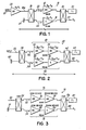
- FIG. 1 illustrates a Doherty amplifier design driven by a Class AB amplifier, as discussed above.
- the Doherty amplifier 10 includes a main or carrier amplifier circuit 12 and an auxiliary amplifier circuit, or peak amplifier circuit 14.
- auxiliary and “peak” will be used interchangeably to indicate the auxiliary amplifier circuit, because the auxiliary amplifier circuit is often made operable based upon the level of the input signal, such as at signal peaks.
- the main amplifier circuit 12 might also be referred to as a carrier amplifier circuit.
- a splitter circuit 16 such as an input coupler, is configured and operable to split an input signal 18 between a path 20 through the main amplifier circuit 12 and a path 22 through the peak amplifier circuit 14.
- the input signal 18 is input into one terminal of the coupler 16, and the other input terminal is appropriately terminated, such as with a 50 ohm load 24.
- the amplifier 10 includes a driver or driving amplifier stage 26, which amplifies the input signal 18 to provide an amplified signal 18a to the Doherty amplifier circuit.
- the outputs of the main amplifier circuit 12 and peak amplifier circuit 14 are appropriately combined, such as with a coupler circuit 30.
- the output of the amplifier is provided at terminal 34, while the other terminal of the coupler circuit 30 is terminated with a suitable load 32.
- Designs of appropriate signal coupling stages and coupler load 32 are illustrated in U.S. Patent No. 6,922,102 and U.S. Patent Application No. 10/795,055 , as noted above.
- Figure 2 illustrates one embodiment of the present invention, which utilizes a multi-stage Doherty amplifier design, including a main amplifier circuit 40 including a driving stage 42 and a main or peak amplifier additional stage 44.
- the amplifier circuit 38 also includes an auxiliary or peak amplifier circuit 46 that includes multiple stages.
- a driving stage 48 precedes an additional stage, such as a peak amplifier stage 50.
- An input signal 52 is split by an appropriate splitter circuit, such as an input coupler 54. The input signal is thus split between a main amplifier circuit path 56 and a peak or auxiliary amplifier circuit path 58.
- the remaining terminal of coupler 54 may be terminated with an appropriate termination, such as a 50-ohm termination 60.
- the outputs of the main amplifier circuit 40 and auxiliary amplifier circuit 46 are combined at coupler 62 where the output terminal 66 provides P o and the other terminal 64 is terminated as discussed above for Figure 1.
- utilizing a multi-stage amplifier circuit for both the main amplifier circuit and auxiliary amplifier circuit provides an immediate system efficiency improvement.
- the output power rating P o for the overall amplifier circuit 10 may be assumed to be the same for both Figures 1 and 2.
- P 1 is the output power rating of the driving stage, such as the power rating for the class AB amplifier 26.
- P M1 and P A1 are the output power ratings of the first stage, or driving stage, of the main and auxiliary amplifier circuits 40, 46, respectively in Figure 2.
- G M1 and G M2 represent the gains of the first and second stages of the main amplifier circuit 40.
- G A1 and G A2 are the respective gains of the various auxiliary amplifier circuit stages.
- G M1 and G A1 refer to the gains of the driving stages of the respective main amplifier circuit 40 and the auxiliary amplifier circuit 46.
- the gain of the overall Doherty amplifier circuit 10 in Figure 1 is designated G D .
- G D2 represents the overall gain of the Doherty amplifier circuit 38 in Figure 2.
- Co(dB) is the output coupler ratio in dB.
- that value will be -3.0 dB.
- P O 56 dBm
- C O -3.0 dB
- G M2 13 dB
- M 3db
- the first stage, or driving stage, of the main amplifier circuit 40 in Figure 2 can be 4.7 dB smaller than, or 1/3 the size of the driving stage 26 in Figure 1.
- a system efficiency improvement is recognized because a portion of the driving stage in Figure 2 that is operating in Class AB mode is 1/3 as large as the Class AB driving stage 26 in Figure 1.
- the auxiliary amplifier 14 should have an RF output current that increases at a significantly greater rate with input drive voltage than the same characteristic for the main amplifier 12. This factor of a 2X greater slope may be achieved in a variety of ways.
- the auxiliary, or peaking, amplifier might use an amplifier device with 2X the periphery or size of the main amplifier device 12. Ideally, this would result in a peaking amplifier 14 with 6 dB more gain than that achieved for the main amplifier 12.
- a peaking amplifier 14 with 6 dB more gain than that achieved for the main amplifier 12.
- such a solution generally has some practical technical difficulties in implementing and is also often impractical from a cost perspective.
- An alternative method is to provide 2X the drive voltage to the peaking, or auxiliary, amplifier circuit 14 in Figure 1 than is provided to the main amplifier circuit 12.
- the coupler would have a value of around 7 dB.
- Such a power loss after the driver amplifier 26 significantly reduces the overall gain of the Doherty amplifier 10 shown in Figure 1. This gain reduction thus requires an even higher power rating for the driver stage 26 and suffers subsequent driver stage inefficiencies that negate the improvement in the Doherty stage efficiency.
- the amplifier of Figure 2 addresses such drawbacks of the circuit in Figure 1 in addition to providing the system efficiency noted above because the driving stage 42 of the main amplifier circuit 40 can be 1/3 the size of the driving stage amplifier 26 of Figure 1.
- FIG. 3 Another embodiment of the present invention that addresses such drawbacks and realises the efficiency improvement desired is shown in Figure 3. More specifically, the embodiment illustrated in Figure 3 utilises a multi-stage Doherty amplifier design 70 including a main amplifier circuit with multiple amplification stages, including a driving stage and an auxiliary amplifier circuit with multiple amplification stages, also including a driving stage. Periphery scaling is utilised between the driving stages of the main amplifier circuit. Furthermore, asymmetric input splitting is utilised in the input signals to the driving stages. In the inventive embodiment show in Figure 3, the auxiliary or peaking amplifier device periphery scaling is performed in the driving stage where it is more technically practical and cost-effective to do so.
- a Doherty type amplifier 70 includes multiple states for both the main amplifier circuit 72 and the auxiliary or peak amplifier circuit 74.
- the main amplifier circuit 72 includes a driving amplification stage 76 and an additional amplification stage 78.
- auxiliary amplifier circuit 74 includes a driving stage 80, as well as an additional stage 82. While two stages are shown for each of the main and auxiliary amplifier circuits, additional stages might also be utilise.
- the multi-stage Doherty design or amplifier 70 incorporates periphery scaling between the driving stages.
- the peak amplifier driving stage 80 is 2X the periphery or size of the main amplifier driving stage 76.
- driving stage 80 incorporates a 40-Watt device in order to satisfy a 20-Watt power-rating requirement.
- the 40-Watt driving stage 80 is intentionally matched to provide more gain at the expense of output power capability for that stage. Due to transistor imperfections, the additional gain that is actually obtained by the periphery scaling of the auxiliary amplifier driving stage 80 only provides a portion of the desired gain asymmetry. While the additional amplification stages 78, 82 for both the main and auxiliary circuits are shown the same power (i.e., 200 Watts), it is not critical that those stages are equal.
- a coupler is utilized to provide additional gain asymmetry that is desired to achieve a more ideal Doherty performance.
- the present invention provides the input signal split prior to the driving stages and, thus, at a much lower power level. This improves the overall system efficiency.
- a -5 dB input coupler 84 is utilized to provide additional gain asymmetry between the main path 92 and the auxiliary path 94.
- the auxiliary path 94 receives the greater portion of the input signal from the asymmetric split provided by coupler 84.
- the main amplifier circuit 72 and peak amplifier circuit 74 are terminated with a suitable termination, such as a -3dB coupler 86 and a suitable termination 87.
- the output power P o (88) is the result of the combined signals from the main and peak amplifier circuits 72, 74.
- An input signal 90 is asymmetrically split by coupler 84. The input signal is split between a main amplifier circuit path 92 and the auxiliary amplifier circuit path 94, and directed to the main and peak amplifier circuits where additional gain asymmetry is employed in the multi-stage Doherty amplifier 70 of the invention.
- An additional input terminal to coupler 84 is terminated with a suitable termination 91, such as a 50-ohm termination.
- an additional characteristic of the auxiliary or peak amplifier circuit 74 is the turn-on point, or input voltage point where the peak amplifier circuit RF output current becomes non-zero.
- the Doherty amplifier operates by generally amplifying the input signal with the main amplifier until the input voltage level rises to the point where the peak amplifier is necessary. Thereafter, the output is a combination of amplified signals from both the main amplifier circuit 72 and peak amplifier circuit 74.
- the turn-on point is generally controlled with a choice of the bias voltage of the peaking amplifier.
- the bias voltage may be the gate bias voltage in the case of a field effect transistor or FET.
- the turn-on point is determined by a single control, which is the gate bias of the single-stage peak amplifier 14.
- the turn-on point for the peak amplifier circuit 74 is determined by the combination of bias voltages, such as gate bias voltages, chosen for the multiple, individual peaking amplifier stages.
- bias voltages such as gate bias voltages
- the present invention provides an increased freedom to tailor the shape of the turn-on characteristic of the peak amplifier circuit 74. This is useful when optimizing the linearity of the overall Doherty amplifier.
- the peak amplifier bias points may be selected experimentally to trade off efficiency with linearity.
- the driving stage 80 of the peak amplifier circuit 74 is not biased as a class AB device similar to the driving stage 76 of the main amplifier circuit 72. Rather, the driving stage 80 is biased close to Class B, or possibly slightly into the A/B or B/C regions. In the embodiment shown in Figure 3, the driving stage 80 is shown to be classified in the B/C region. Then, the additional stage 82 of the peak amplifier circuit 74 is biased further into a Class C region than the preceding driving stage 80. Therefore, it is desirable to bias the multiple stages in the peak amplifier circuit 74 to achieve greater efficiency. It is particularly desirable to bias the stages 82 following the driving stage 80 to an operation point that yields greater efficiency.
- the amplifier utilises a combination of amplifier device periphery scaling and asymmetric input splitting in combination with multi-stage main and peak amplifier circuits to more effectively improve overall efficiency. Furthermore, the amplifier provides multiple turn-on characteristics for the peak amplifier circuit 74 to yield a more
Landscapes
- Engineering & Computer Science (AREA)
- Power Engineering (AREA)
- Amplifiers (AREA)
Abstract
Description
- This invention is directed generally to RF power amplifiers and more particularly to improving the overall efficiency of high power RF power amplifiers while maintaining desirable system linearity.
- In the design of RF power amplifiers, such as for RF communication applications, it is desirable to improve the efficiency of an amplifier or amplification system while maintaining a desirable system linearity. Linearity and efficiency are often competing design characteristics when configuring a suitable RF amplification system. While linearity is required to reduce interference between adjacent RF signals in a band, to maintain the amplified signals in the band and to reduce distortion, the most linear amplifiers are also usually the most inefficient.
- There have been various different amplifier designs utilized to improve efficiency. One design is the Doherty-type or Doherty amplifier, which utilizes a main amplifier or carrier, and an auxiliary or peaking amplifier to handle higher input signal levels. That is, in a certain range of input signal level, generally only the main amplifier is operational and providing the desired signal gain. However, at a higher input signal level, the auxiliary amplifier also begins to operate and contributes to the overall gain of the Doherty amplifier.
- Doherty amplifiers offer a method of improving RF/microwave amplifier efficiency over that achieved by traditional Class AB amplifiers. The benefit is achieved when the Doherty amplifier operates at a power level that is backed off from the maximum power achievable at the amplifier output. Some examples of Doherty amplifier designs are set forth in
U.S. Patent No. 6,922,102 , entitled "High Efficiency Amplifier" andU.S. Patent Application Serial No. 10/795,055 , entitled "High Efficiency Amplifier and Method of Designing Same". - Generally, in most applications, the power gain of such a Doherty amplifier is not sufficient to provide the entire gain required by the power amplifier. In such cases, the Doherty amplifier is preceded by at least one additional gain or amplification stage. Typically, the gain stage immediately preceding the Doherty stage is a Class AB device as illustrated in Figure 1. This choice is generally a compromise between efficiency and linearity, considering the degradation in system efficiency that would occur if the driver stage were a Class A amplifier, and considering the degradation in system linearity that would occur if the driver stage were also a Doherty amplifier.
- However, a driver stage that is also a Doherty amplifier offers better overall system efficiency, even though overall system linearity might be degraded when compared to using a Class A and Class AB driver stage. The existing design as shown in Figure 1 does not achieve the desired efficiency. Therefore, it is still desirable to achieve better overall system efficiency by improving the driver stage efficiency without suffering a significant loss in system linearity.
- The present invention utilises a Doherty amplifier with a main amplifier circuit and an auxiliary amplifier circuit, both including multiple amplification stages in combination with efficiency enhancing aspects. Each of the amplifier circuits of the amplifier includes a driving stage. In accordance with one aspect of the present invention, the driving stage of the auxiliary amplifier circuit has a power rating that is higher than the power rating of the main amplifier circuit to provide a gain asymmetry in the amplifier circuit paths. In accordance with another aspect of the present invention, a coupler is utilised to provide an asymmetric split of the input signal to the various paths through the auxiliary amplifier circuit and the main amplifier circuit. In accordance with still another aspect of the present invention, the auxiliary amplifier circuit has a turn-on characteristic that is determined by a combination of bias conditions for the multiple stages of the auxiliary amplifier circuit. As such, the present invention provides a method of improving overall amplifier efficiency, by improving driver efficiency without significant degradation to system linearly.
- The invention will now be described by way of example with reference to the accompanying drawings in which:
- Figure 1 illustrates a block diagram of an amplifier using a Doherty-type amplification stage.
- Figure 2 is a block diagram of one embodiment of the invention.
- Figure 3 is a block diagram of another embodiment of the invention.
- Figure 1 illustrates a Doherty amplifier design driven by a Class AB amplifier, as discussed above. The Doherty
amplifier 10 includes a main or carrier amplifier circuit 12 and an auxiliary amplifier circuit, orpeak amplifier circuit 14. Herein, the terms "auxiliary" and "peak" will be used interchangeably to indicate the auxiliary amplifier circuit, because the auxiliary amplifier circuit is often made operable based upon the level of the input signal, such as at signal peaks. Similarly, the main amplifier circuit 12 might also be referred to as a carrier amplifier circuit. Asplitter circuit 16, such as an input coupler, is configured and operable to split aninput signal 18 between a path 20 through the main amplifier circuit 12 and apath 22 through thepeak amplifier circuit 14. Theinput signal 18 is input into one terminal of thecoupler 16, and the other input terminal is appropriately terminated, such as with a 50ohm load 24. Theamplifier 10 includes a driver ordriving amplifier stage 26, which amplifies theinput signal 18 to provide an amplified signal 18a to the Doherty amplifier circuit. The outputs of the main amplifier circuit 12 andpeak amplifier circuit 14 are appropriately combined, such as with acoupler circuit 30. The output of the amplifier is provided atterminal 34, while the other terminal of thecoupler circuit 30 is terminated with asuitable load 32. Designs of appropriate signal coupling stages andcoupler load 32 are illustrated inU.S. Patent No. 6,922,102 andU.S. Patent Application No. 10/795,055 , as noted above. - Figure 2 illustrates one embodiment of the present invention, which utilizes a multi-stage Doherty amplifier design, including a
main amplifier circuit 40 including adriving stage 42 and a main or peak amplifieradditional stage 44. Theamplifier circuit 38 also includes an auxiliary orpeak amplifier circuit 46 that includes multiple stages. In the embodiment of Figure 2, adriving stage 48 precedes an additional stage, such as a peak amplifier stage 50. An input signal 52 is split by an appropriate splitter circuit, such as aninput coupler 54. The input signal is thus split between a mainamplifier circuit path 56 and a peak or auxiliaryamplifier circuit path 58. The remaining terminal ofcoupler 54 may be terminated with an appropriate termination, such as a 50-ohm termination 60. The outputs of themain amplifier circuit 40 andauxiliary amplifier circuit 46 are combined atcoupler 62 where theoutput terminal 66 provides Po and theother terminal 64 is terminated as discussed above for Figure 1. - In accordance with one aspect of the present invention, utilizing a multi-stage amplifier circuit for both the main amplifier circuit and auxiliary amplifier circuit provides an immediate system efficiency improvement. For example, referring to Figure 1, the output power rating Po for the
overall amplifier circuit 10 may be assumed to be the same for both Figures 1 and 2. In Figure 1, P1 is the output power rating of the driving stage, such as the power rating for theclass AB amplifier 26. PM1 and PA1 are the output power ratings of the first stage, or driving stage, of the main andauxiliary amplifier circuits main amplifier circuit 40. GA1 and GA2 are the respective gains of the various auxiliary amplifier circuit stages. For example, GM1 and GA1 refer to the gains of the driving stages of the respectivemain amplifier circuit 40 and theauxiliary amplifier circuit 46. The gain of the overall Dohertyamplifier circuit 10 in Figure 1 is designated GD. GD2 represents the overall gain of the Dohertyamplifier circuit 38 in Figure 2. - Due to non-ideal operation in the RF transistor output impedance and also typical peaking amplifier drive-up characteristics, Doherty amplifiers typically have less power gain than is achieved in a balanced AB amplifier made with the same pair of transistors. The amount of power degradation is typically in the range of 1-2 dB. This decreasing gain effectively appears at the input split of the Doherty amplifier and must be accounted for when determining the driving stage power rating P1 (see Figure 1). For example, with GM = GA = 13 dB in Figure 1, the overall GD would typically be 11-12 dB. The driving stage power rating P1 would then be set forth by Equation 1:

- M (dB) is the additional back-off margin required for the
driving stage amplifier 26. This may be assumed to be 3 dB, but will vary with design specifics. As an example, with the output power rating PO = 56 dBm, GD = 11.25 dB, then P1 =47.75dBm. - Turning now to Figure 2, and assuming no output losses, the driving stage power rating PM1 for the
driving stage 42 of themain amplifier circuit 40 is set forth by Equation 2, as follows:
- Co(dB) is the output coupler ratio in dB. Generally, for equal main auxiliary amplifier ratings, that value will be -3.0 dB. With the power output rating PO = 56 dBm, CO = -3.0 dB, GM2 = 13 dB, and M = 3db, then the output power rating PM1 for the
driving stage 42 ofmain amplifier circuit 40 becomes 43 dBm. - Therefore, utilizing a multi-stage Doherty amplifier, as illustrated in Figure 2, the first stage, or driving stage, of the
main amplifier circuit 40 in Figure 2 can be 4.7 dB smaller than, or 1/3 the size of the drivingstage 26 in Figure 1. As such, a system efficiency improvement is recognized because a portion of the driving stage in Figure 2 that is operating in Class AB mode is 1/3 as large as the ClassAB driving stage 26 in Figure 1. - For the embodiment of the
Doherty amplifier 10, illustrated in Figure 1, in order to achieve an efficiency characteristic that approaches that of an ideal Doherty amplifier, theauxiliary amplifier 14 should have an RF output current that increases at a significantly greater rate with input drive voltage than the same characteristic for the main amplifier 12. This factor of a 2X greater slope may be achieved in a variety of ways. - In one way, the auxiliary, or peaking, amplifier might use an amplifier device with 2X the periphery or size of the main amplifier device 12. Ideally, this would result in a peaking
amplifier 14 with 6 dB more gain than that achieved for the main amplifier 12. However, such a solution generally has some practical technical difficulties in implementing and is also often impractical from a cost perspective. - An alternative method is to provide 2X the drive voltage to the peaking, or auxiliary,
amplifier circuit 14 in Figure 1 than is provided to the main amplifier circuit 12. This might be accomplished by placing an asymmetric coupler at the Doherty input with the high loss arm of the coupler connected to the main amplifier input and the lower loss arm coupled to the auxiliary amplifier input. For the case where both the main and auxiliary amplifier output power ratings are equal, the coupler would have a value of around 7 dB. Such a power loss after thedriver amplifier 26 significantly reduces the overall gain of theDoherty amplifier 10 shown in Figure 1. This gain reduction thus requires an even higher power rating for thedriver stage 26 and suffers subsequent driver stage inefficiencies that negate the improvement in the Doherty stage efficiency. The amplifier of Figure 2 addresses such drawbacks of the circuit in Figure 1 in addition to providing the system efficiency noted above because the drivingstage 42 of themain amplifier circuit 40 can be 1/3 the size of the drivingstage amplifier 26 of Figure 1. - Another embodiment of the present invention that addresses such drawbacks and realises the efficiency improvement desired is shown in Figure 3. More specifically, the embodiment illustrated in Figure 3 utilises a multi-stage
Doherty amplifier design 70 including a main amplifier circuit with multiple amplification stages, including a driving stage and an auxiliary amplifier circuit with multiple amplification stages, also including a driving stage. Periphery scaling is utilised between the driving stages of the main amplifier circuit. Furthermore, asymmetric input splitting is utilised in the input signals to the driving stages. In the inventive embodiment show in Figure 3, the auxiliary or peaking amplifier device periphery scaling is performed in the driving stage where it is more technically practical and cost-effective to do so. Additional gain asymmetry that is required between the main and auxiliary amplifier circuits is then provided by the choice of an input coupler value providing asymmetric splitting of the input signal. When multi-stage main and auxiliary amplifier circuits are utilised, the asymmetric split of the input signal occurs at a much lower power level. Therefore, the asymmetric split has less of a negative impact on system efficiency, as opposed to the example set forth above in Figure 1, wherein the input splitting occurs after a driving amplifier. This allows the improvement and efficiency provided by the Doherty amplifier that results from a more ideal auxiliary amplifier drive-up characteristic to be more fully realised. - In the exemplary embodiment of the invention set forth in Figure 3, a
Doherty type amplifier 70 includes multiple states for both themain amplifier circuit 72 and the auxiliary orpeak amplifier circuit 74. Specifically, themain amplifier circuit 72 includes a drivingamplification stage 76 and anadditional amplification stage 78. Similarly,auxiliary amplifier circuit 74 includes a drivingstage 80, as well as anadditional stage 82. While two stages are shown for each of the main and auxiliary amplifier circuits, additional stages might also be utilise. - In accordance with another aspect of the present invention, the multi-stage Doherty design or
amplifier 70 incorporates periphery scaling between the driving stages. Specifically, the peakamplifier driving stage 80 is 2X the periphery or size of the mainamplifier driving stage 76. For example, as shown in Figure 3, if drivingstage 76 incorporates a 20-Watt device, drivingstage 80 incorporates a 40-Watt device in order to satisfy a 20-Watt power-rating requirement. The 40-Watt driving stage 80 is intentionally matched to provide more gain at the expense of output power capability for that stage. Due to transistor imperfections, the additional gain that is actually obtained by the periphery scaling of the auxiliaryamplifier driving stage 80 only provides a portion of the desired gain asymmetry. While the additional amplification stages 78, 82 for both the main and auxiliary circuits are shown the same power (i.e., 200 Watts), it is not critical that those stages are equal. - In accordance with another aspect of the present invention, a coupler is utilized to provide additional gain asymmetry that is desired to achieve a more ideal Doherty performance. As noted above, the present invention provides the input signal split prior to the driving stages and, thus, at a much lower power level. This improves the overall system efficiency. In the embodiment illustrated in Figure 3, a -5
dB input coupler 84 is utilized to provide additional gain asymmetry between themain path 92 and theauxiliary path 94. Theauxiliary path 94 receives the greater portion of the input signal from the asymmetric split provided bycoupler 84. Themain amplifier circuit 72 andpeak amplifier circuit 74 are terminated with a suitable termination, such as a -3dB coupler 86 and asuitable termination 87. As noted above, various suitable terminations are recited in the patent and application mentioned above. The output power Po (88) is the result of the combined signals from the main andpeak amplifier circuits coupler 84. The input signal is split between a mainamplifier circuit path 92 and the auxiliaryamplifier circuit path 94, and directed to the main and peak amplifier circuits where additional gain asymmetry is employed in themulti-stage Doherty amplifier 70 of the invention. An additional input terminal tocoupler 84 is terminated with a suitable termination 91, such as a 50-ohm termination. - In accordance with another aspect of the present invention, an additional characteristic of the auxiliary or
peak amplifier circuit 74 is the turn-on point, or input voltage point where the peak amplifier circuit RF output current becomes non-zero. As understood by a person of ordinary skill in the art, the Doherty amplifier operates by generally amplifying the input signal with the main amplifier until the input voltage level rises to the point where the peak amplifier is necessary. Thereafter, the output is a combination of amplified signals from both themain amplifier circuit 72 andpeak amplifier circuit 74. The turn-on point is generally controlled with a choice of the bias voltage of the peaking amplifier. In one example, the bias voltage may be the gate bias voltage in the case of a field effect transistor or FET. - Generally, in the
amplifier circuit 10, illustrated in Figure 1, the turn-on point is determined by a single control, which is the gate bias of the single-stage peak amplifier 14. However, in accordance with the aspects of the present invention, in the multi-stage amplifier design illustrated in Figure 3, the turn-on point for thepeak amplifier circuit 74 is determined by the combination of bias voltages, such as gate bias voltages, chosen for the multiple, individual peaking amplifier stages. Generally, in an ideal situation, the turn-on point would be a sharp increase from zero in the peak amplifier RF output current. However, generally, actual transistors will have a more gradual turn-on characteristic. In accordance with one aspect of the present invention, cascading one or more turn-on characteristics based upon the cascadedmultiple stages peak amplifier circuit 74, the present invention provides an increased freedom to tailor the shape of the turn-on characteristic of thepeak amplifier circuit 74. This is useful when optimizing the linearity of the overall Doherty amplifier. - In the embodiment illustrated in Figure 3, the peak amplifier bias points may be selected experimentally to trade off efficiency with linearity. In the example set forth in Figure 3, the driving
stage 80 of thepeak amplifier circuit 74 is not biased as a class AB device similar to the drivingstage 76 of themain amplifier circuit 72. Rather, the drivingstage 80 is biased close to Class B, or possibly slightly into the A/B or B/C regions. In the embodiment shown in Figure 3, the drivingstage 80 is shown to be classified in the B/C region. Then, theadditional stage 82 of thepeak amplifier circuit 74 is biased further into a Class C region than the preceding drivingstage 80. Therefore, it is desirable to bias the multiple stages in thepeak amplifier circuit 74 to achieve greater efficiency. It is particularly desirable to bias thestages 82 following the drivingstage 80 to an operation point that yields greater efficiency. - Accordingly, the amplifier utilises a combination of amplifier device periphery scaling and asymmetric input splitting in combination with multi-stage main and peak amplifier circuits to more effectively improve overall efficiency. Furthermore, the amplifier provides multiple turn-on characteristics for the
peak amplifier circuit 74 to yield a more - While the present invention has been illustrated by a description of various embodiments and while these embodiments have been described in considerable detail, additional advantages and modifications will readily appear to those skilled in the art.
Claims (19)
- An amplifier comprising a main amplifier circuit with multiple amplification stages, including a driving stage, an auxiliary amplifier circuit with multiple amplification stages, including a driving stage, the auxiliary amplifier circuit being selectively operable to operate in combination with the main amplifier circuit, a splitter circuit operable to split an input signal to the amplifier between paths through the main amplifier circuit and the auxiliary amplifier circuit, the driving stage of the auxiliary amplifier circuit having a power rating higher than the power rating of the driving stage of the main amplifier circuit to provide a gain asymmetry in the amplifier circuit paths.
- The amplifier of claim 1 wherein the splitter circuit is an input coupler that is operable to provide path asymmetry in splitting the input signal between the main amplifier path and auxiliary amplifier path.
- An amplifier comprising a main amplifier circuit with multiple amplification stages, including a driving stage, an auxiliary amplifier circuit with multiple amplification stages, including a driving stage, the auxiliary amplifier circuit being selectively operable to operate in combination with the main amplifier circuit, a splitter circuit operable to split an input signal to the amplifier between paths through the main amplifier circuit and the auxiliary amplifier circuit and operable to provide path asymmetry in splitting the input signal between the paths.
- The amplifier of claim 3 wherein the splitter circuit includes an input coupler for coupling portions of the input signal onto the paths.
- The amplifier of either claim 2 or claim 4 wherein the input coupler is a -5 dB coupler configured to provide a greater input signal portion in the auxiliary amplifier path.
- An amplifier comprising a main amplifier circuit, an auxiliary amplifier circuit, the auxiliary amplifier circuit being selectively operable, based on a turn-on characteristic, to operate in combination with the main amplifier circuit, the auxiliary circuit having multiple amplification stages.
- The amplifier of claim 6 wherein the main amplifier circuit and auxiliary amplifier circuit each include multiple amplification stages.
- The amplifier of any preceding claim wherein the auxiliary amplifier circuit has a turn-on characteristic dependent upon bias, the turn-on characteristic being determined by a combination of bias conditions for the multiple stages of the auxiliary amplifier circuit.
- The amplifier of claim 8 wherein the driving stage of the auxiliary amplifier circuit has a bias condition to place the driving stage in on one of a Class B, Class A/B or Class B/C region.
- The amplifier of either claim 8 or claim 9 wherein the additional stage of the auxiliary amplifier circuit has a bias condition to place the additional stage in approximately a Class C region.
- The amplifier of any preceding claim further comprising a coupler circuit coupled to combine the outputs of the main amplifier circuit and the auxiliary amplifier circuit.
- A method of amplifying a signal comprising splitting an input signal between a main amplifier circuit with multiple amplification stages, including a driving stage and an auxiliary amplifier circuit with multiple stages, including a driving stage, selectively operating the auxiliary amplifier circuit to operate in combination with the main amplifier circuit, the driving stage of the auxiliary amplifier circuit having a power rating higher than the power rating of the main amplifier circuit to provide a gain asymmetry in the amplifier circuit paths.
- The method of claim 12 further comprising splitting the input signal to provide path asymmetry between a main amplifier path and an auxiliary amplifier path.
- A method of amplifying a signal comprising inputting an input signal between a main amplifier circuit with multiple amplification stages, including a driving stage and an auxiliary amplifier circuit with multiple stages, including a driving stage, selectively operating the auxiliary amplifier circuit to operate in combination with the main amplifier circuit, splitting the input signal asymmetrically between paths through the main amplifier circuit and the auxiliary amplifier circuit.
- The method of claim 14 further comprising splitting the input signal to provide a greater input signal portion in the auxiliary amplifier path.
- A method of amplifying a signal comprising inputting an input signal between a main amplifier circuit and an auxiliary amplifier circuit, selectively operating the auxiliary amplifier circuit to operate in combination with the main amplifier circuit, splitting the input signal asymmetrically between paths through the main amplifier circuit and the auxiliary amplifier circuit.
- The method of any one of claims 12 to 16 wherein the auxiliary amplifier circuit has a turn-on characteristic dependent upon bias, and further comprising establishing the turn-on characteristic by a combination of bias conditions for the multiple stages of the auxiliary amplifier circuit.
- The method of claim 17 further comprising biasing the driving stage of the auxiliary amplifier circuit to place the driving stage in on one of a Class B, Class A/B or Class B/C region.
- The method of either claim 17 or claim 18 further comprising biasing an additional stage of the auxiliary amplifier circuit to place the additional stage in approximately a Class C region.
Applications Claiming Priority (1)
| Application Number | Priority Date | Filing Date | Title |
|---|---|---|---|
| US11/291,172 US7362170B2 (en) | 2005-12-01 | 2005-12-01 | High gain, high efficiency power amplifier |
Publications (2)
| Publication Number | Publication Date |
|---|---|
| EP1793490A1 true EP1793490A1 (en) | 2007-06-06 |
| EP1793490B1 EP1793490B1 (en) | 2009-04-29 |
Family
ID=37670668
Family Applications (1)
| Application Number | Title | Priority Date | Filing Date |
|---|---|---|---|
| EP06254052A Not-in-force EP1793490B1 (en) | 2005-12-01 | 2006-08-02 | Doherty power amplifier with improved efficiency |
Country Status (5)
| Country | Link |
|---|---|
| US (1) | US7362170B2 (en) |
| EP (1) | EP1793490B1 (en) |
| KR (1) | KR101261055B1 (en) |
| CN (1) | CN1976217B (en) |
| DE (1) | DE602006006526D1 (en) |
Cited By (6)
| Publication number | Priority date | Publication date | Assignee | Title |
|---|---|---|---|---|
| EP2393201A1 (en) * | 2010-06-02 | 2011-12-07 | Nxp B.V. | Two stage doherty amplifier |
| EP2933918A1 (en) * | 2014-04-15 | 2015-10-21 | Nxp B.V. | Ultra wideband doherty amplifier |
| WO2015169909A1 (en) * | 2014-05-07 | 2015-11-12 | Advanced Wireless Solutions And Services (Aw2S) | Radiofrequency amplification system |
| EP2947768A1 (en) * | 2014-05-19 | 2015-11-25 | Nokia Solutions and Networks GmbH & Co. KG | Load modulation amplification with enhanced load modulation ratio |
| US9325280B2 (en) | 2007-09-03 | 2016-04-26 | Ampleon Netherlands B.V. | Multi-way doherty amplifier |
| CN105932970A (en) * | 2016-04-18 | 2016-09-07 | 北京邮电大学 | Envelope tracked Doherty power amplifier |
Families Citing this family (41)
| Publication number | Priority date | Publication date | Assignee | Title |
|---|---|---|---|---|
| US7710202B2 (en) * | 2003-09-17 | 2010-05-04 | Nec Corporation | Amplifier |
| US7936212B2 (en) * | 2008-05-09 | 2011-05-03 | Cree, Inc. | Progressive power generating amplifiers |
| US7888999B2 (en) * | 2008-07-09 | 2011-02-15 | Loopcomm Technology Inc. | Premium power amplifier |
| CN101582682B (en) * | 2009-06-12 | 2011-12-28 | 华为技术有限公司 | Power amplifier and transmitter |
| EP2905895A1 (en) * | 2009-09-28 | 2015-08-12 | NEC Corporation | Doherty amplifier |
| US9484613B1 (en) * | 2010-01-29 | 2016-11-01 | United States Of America As Represented By The Administrator Of National Aeronautics And Space Administration | Ka-band waveguide 2-way hybrid combiner for MMIC amplifiers with unequal and arbitrary power output ratio |
| US20120007674A1 (en) * | 2010-07-06 | 2012-01-12 | Korea Advanced Institute Of Science And Technology | Power amplifier reducing gain mismatch |
| US8860529B2 (en) | 2010-09-10 | 2014-10-14 | Anaren, Inc. | Impedance transforming coupler |
| US9083284B2 (en) | 2011-03-07 | 2015-07-14 | Intel Corporation | Wide-band multi stage Doherty power amplifier |
| US9419566B2 (en) | 2011-04-20 | 2016-08-16 | Freescale Semiconductor, Inc. | Amplifiers and related integrated circuits |
| CN102185563B (en) * | 2011-04-29 | 2016-03-02 | 中兴通讯股份有限公司 | A kind of Doherty power amplification device |
| CN102158190A (en) * | 2011-04-29 | 2011-08-17 | 中兴通讯股份有限公司 | Doherty power amplifier and implementation method thereof |
| EP2721732A1 (en) * | 2011-06-20 | 2014-04-23 | Telefonaktiebolaget LM Ericsson (PUBL) | Power amplifier based on doherty power amplifier |
| US9742365B1 (en) * | 2011-12-15 | 2017-08-22 | Kenneth Sean Ozard | Doherty amplifier |
| US8829998B2 (en) * | 2012-10-23 | 2014-09-09 | Airspan Networks Inc. | Doherty power amplifier |
| US8952758B2 (en) | 2013-04-23 | 2015-02-10 | Freescale Semiconductor, Inc. | Amplifier using nonlinear drivers |
| US9397617B2 (en) | 2013-06-25 | 2016-07-19 | Rf Micro Devices, Inc. | Multi-broadband Doherty power amplifier |
| US9407214B2 (en) | 2013-06-28 | 2016-08-02 | Cree, Inc. | MMIC power amplifier |
| US9948243B2 (en) * | 2013-09-30 | 2018-04-17 | Qorvo Us, Inc. | Reconfigurable load modulation amplifier |
| US9484865B2 (en) | 2013-09-30 | 2016-11-01 | Qorvo Us, Inc. | Reconfigurable load modulation amplifier |
| US9397616B2 (en) * | 2013-11-06 | 2016-07-19 | Commscope Technologies Llc | Quasi-doherty architecture amplifier and method |
| US9473275B2 (en) | 2013-11-13 | 2016-10-18 | Mediatek Singapore Pte. Ltd. | Gain asymmetry characterizing circuit and method for determining characteristics of gain asymmetry possessed by transmitter |
| US9628027B2 (en) | 2014-03-14 | 2017-04-18 | Nxp Usa, Inc. | Multi-path devices with mutual inductance compensation networks and methods thereof |
| US20150295540A1 (en) * | 2014-04-11 | 2015-10-15 | Auriga Measurement Systems, LLC | Outphasing power amplifier having unbalanced drive power |
| JP6384105B2 (en) * | 2014-04-22 | 2018-09-05 | 三菱電機株式会社 | Power amplifier |
| US9912298B2 (en) | 2014-05-13 | 2018-03-06 | Skyworks Solutions, Inc. | Systems and methods related to linear load modulated power amplifiers |
| EP3145078B1 (en) | 2014-05-28 | 2018-09-19 | Huawei Technologies Co., Ltd. | Doherty power amplifier and transmitter |
| US9800207B2 (en) * | 2014-08-13 | 2017-10-24 | Skyworks Solutions, Inc. | Doherty power amplifier combiner with tunable impedance termination circuit |
| US9712119B2 (en) * | 2014-10-25 | 2017-07-18 | Skyworks Solutions, Inc. | Doherty power amplifier with tunable input network |
| US9979356B2 (en) | 2014-12-17 | 2018-05-22 | Nxp Usa, Inc. | Magnetically coupled load modulation |
| US11245363B2 (en) * | 2017-04-24 | 2022-02-08 | Macom Technology Solutions Holdings, Inc. | Efficiency, symmetrical Doherty power amplifier |
| US10250197B1 (en) | 2017-11-06 | 2019-04-02 | Nxp Usa, Inc. | Multiple-stage power amplifiers implemented with multiple semiconductor technologies |
| EP3480945A1 (en) | 2017-11-06 | 2019-05-08 | NXP USA, Inc. | Multiple-stage power amplifiers implemented with multiple semiconductor technologies |
| US11251762B2 (en) * | 2018-01-22 | 2022-02-15 | Mitsubishi Electric Corporation | Amplifier |
| US10530306B2 (en) | 2018-04-13 | 2020-01-07 | Nxp Usa, Inc. | Hybrid power amplifier circuit or system with combination low-pass and high-pass interstage circuitry and method of operating same |
| US11094507B2 (en) | 2019-07-22 | 2021-08-17 | Tokyo Electron Limited | Power generation systems and methods for plasma stability and control |
| US11218118B2 (en) | 2020-03-30 | 2022-01-04 | Analog Devices International Unlimited Company | Linearity optimizer for a millimeter-wave beamforming system |
| CN115706566A (en) * | 2021-08-04 | 2023-02-17 | 中兴通讯股份有限公司 | Power amplification circuit, base station, signal transceiving equipment and power amplification device |
| CN114189215B (en) * | 2021-10-29 | 2024-08-30 | 锐石创芯(深圳)科技股份有限公司 | RF power amplifier circuit and RF front-end module |
| CN117013972A (en) * | 2022-04-28 | 2023-11-07 | 苏州华太电子技术股份有限公司 | Power amplifying device and method for controlling the same |
| US12483196B2 (en) | 2022-12-27 | 2025-11-25 | Nxp Usa, Inc. | Multiple-mode RF power amplifiers |
Citations (3)
| Publication number | Priority date | Publication date | Assignee | Title |
|---|---|---|---|---|
| WO2004023646A1 (en) * | 2002-09-06 | 2004-03-18 | Filtronic Plc | Class-f doherty amplifier |
| WO2004088837A2 (en) * | 2003-03-28 | 2004-10-14 | Andrew Corporation | Doherty amplifier with output hybrid coupler |
| EP1583228A2 (en) * | 2002-01-16 | 2005-10-05 | Telefonaktiebolaget LM Ericsson (publ) | Composite power amplifier |
Family Cites Families (39)
| Publication number | Priority date | Publication date | Assignee | Title |
|---|---|---|---|---|
| US2210028A (en) * | 1936-04-01 | 1940-08-06 | Bell Telephone Labor Inc | Amplifier |
| US2255476A (en) * | 1939-02-09 | 1941-09-09 | Gen Electric | High efficiency amplifier |
| BE510734A (en) * | 1951-04-19 | |||
| DE3906448C1 (en) | 1989-03-01 | 1990-03-15 | Messerschmitt-Boelkow-Blohm Gmbh, 8012 Ottobrunn, De | |
| US5420541A (en) * | 1993-06-04 | 1995-05-30 | Raytheon Company | Microwave doherty amplifier |
| US5568086A (en) * | 1995-05-25 | 1996-10-22 | Motorola, Inc. | Linear power amplifier for high efficiency multi-carrier performance |
| US5739723A (en) * | 1995-12-04 | 1998-04-14 | Motorola, Inc. | Linear power amplifier using active bias for high efficiency and method thereof |
| US5786727A (en) * | 1996-10-15 | 1998-07-28 | Motorola, Inc. | Multi-stage high efficiency linear power amplifier and method therefor |
| US6268770B1 (en) * | 1998-07-17 | 2001-07-31 | Anthony T. Barbetta | Wide bandwidth, current sharing, MOSFET audio power amplifier with multiple feedback loops |
| US6085074A (en) * | 1997-02-28 | 2000-07-04 | Motorola, Inc. | Apparatus and method for amplifying an amplitude-varying signal |
| US5880633A (en) * | 1997-05-08 | 1999-03-09 | Motorola, Inc. | High efficiency power amplifier |
| US6097252A (en) * | 1997-06-02 | 2000-08-01 | Motorola, Inc. | Method and apparatus for high efficiency power amplification |
| US5966059A (en) * | 1997-09-02 | 1999-10-12 | Motorola, Inc. | Phase shifting power coupler with three signals of equal amplitude |
| US6285251B1 (en) * | 1998-04-02 | 2001-09-04 | Ericsson Inc. | Amplification systems and methods using fixed and modulated power supply voltages and buck-boost control |
| US6359506B1 (en) | 1998-04-02 | 2002-03-19 | Ericsson Inc. | Linear modulation using a linear and a non-linear amplifier |
| EP1041712B1 (en) * | 1999-03-31 | 2009-01-28 | NTT Mobile Communications Network Inc. | Feedforward amplifier |
| US6329877B1 (en) * | 1999-06-25 | 2001-12-11 | Agere Systems Guardian Corp. | Efficient power amplifier |
| US6262629B1 (en) * | 1999-07-06 | 2001-07-17 | Motorola, Inc. | High efficiency power amplifier having reduced output matching networks for use in portable devices |
| SE520760C2 (en) * | 2000-06-06 | 2003-08-19 | Ericsson Telefon Ab L M | Doherty multistage amplifier |
| SE516847C2 (en) * | 2000-07-07 | 2002-03-12 | Ericsson Telefon Ab L M | Composite amplifier and transmitter including such amplifier |
| US6396341B1 (en) * | 2000-12-29 | 2002-05-28 | Ericsson Inc. | Class E Doherty amplifier topology for high efficiency signal transmitters |
| US6731172B2 (en) * | 2001-01-16 | 2004-05-04 | Skyworks Solutions, Inc. | Doherty power amplifier with integrated quarter wave transformer/combiner circuit |
| US20020186079A1 (en) | 2001-06-08 | 2002-12-12 | Kobayashi Kevin W. | Asymmetrically biased high linearity balanced amplifier |
| US6864742B2 (en) * | 2001-06-08 | 2005-03-08 | Northrop Grumman Corporation | Application of the doherty amplifier as a predistortion circuit for linearizing microwave amplifiers |
| US6917246B2 (en) * | 2001-09-10 | 2005-07-12 | Skyworks Solutions, Inc. | Doherty bias circuit to dynamically compensate for process and environmental variations |
| US6791417B2 (en) * | 2002-01-28 | 2004-09-14 | Cree Microwave, Inc. | N-way RF power amplifier circuit with increased back-off capability and power added efficiency using selected phase lengths and output impedances |
| US6700444B2 (en) * | 2002-01-28 | 2004-03-02 | Cree Microwave, Inc. | N-way RF power amplifier with increased backoff power and power added efficiency |
| US6737922B2 (en) * | 2002-01-28 | 2004-05-18 | Cree Microwave, Inc. | N-way RF power amplifier circuit with increased back-off capability and power added efficiency using unequal input power division |
| KR100450744B1 (en) * | 2002-08-29 | 2004-10-01 | 학교법인 포항공과대학교 | Doherty amplifier |
| KR100480496B1 (en) * | 2002-11-18 | 2005-04-07 | 학교법인 포항공과대학교 | Signal amplifier by using a doherty amplifier |
| US6798295B2 (en) * | 2002-12-13 | 2004-09-28 | Cree Microwave, Inc. | Single package multi-chip RF power amplifier |
| JP2004221646A (en) | 2003-01-09 | 2004-08-05 | Nec Corp | Doherty amplifier |
| KR20040079597A (en) * | 2003-03-08 | 2004-09-16 | 학교법인 포항공과대학교 | The microwave doherty amplifier apparatus by using adaptive bias control technique |
| US6922102B2 (en) * | 2003-03-28 | 2005-07-26 | Andrew Corporation | High efficiency amplifier |
| US6853244B2 (en) * | 2003-06-24 | 2005-02-08 | Northrop Grumman Corproation | Multi-mode multi-amplifier architecture |
| US7042287B2 (en) * | 2003-07-23 | 2006-05-09 | Northrop Grumman Corporation | System and method for reducing dynamic range and improving linearity in an amplication system |
| KR20050031663A (en) | 2003-09-30 | 2005-04-06 | 광운대학교 산학협력단 | Doherty power amplifying apparatus |
| US7295065B2 (en) * | 2004-11-18 | 2007-11-13 | Beecem Communications Inc. | High efficiency doherty amplifier with a segmented main amplifier |
| US7193473B2 (en) * | 2005-03-24 | 2007-03-20 | Cree, Inc. | High power Doherty amplifier using multi-stage modules |
-
2005
- 2005-12-01 US US11/291,172 patent/US7362170B2/en not_active Expired - Lifetime
-
2006
- 2006-07-24 KR KR1020060068948A patent/KR101261055B1/en not_active Expired - Fee Related
- 2006-08-02 EP EP06254052A patent/EP1793490B1/en not_active Not-in-force
- 2006-08-02 DE DE602006006526T patent/DE602006006526D1/en active Active
- 2006-10-27 CN CN2006101429679A patent/CN1976217B/en not_active Expired - Fee Related
Patent Citations (3)
| Publication number | Priority date | Publication date | Assignee | Title |
|---|---|---|---|---|
| EP1583228A2 (en) * | 2002-01-16 | 2005-10-05 | Telefonaktiebolaget LM Ericsson (publ) | Composite power amplifier |
| WO2004023646A1 (en) * | 2002-09-06 | 2004-03-18 | Filtronic Plc | Class-f doherty amplifier |
| WO2004088837A2 (en) * | 2003-03-28 | 2004-10-14 | Andrew Corporation | Doherty amplifier with output hybrid coupler |
Non-Patent Citations (2)
| Title |
|---|
| GAJADHARSING J R ET AL: "Analysis and design of a 200W LDMOS based doherty amplifier for 3G base stations", MICROWAVE SYMPOSIUM DIGEST, 2004 IEEE MTT-S INTERNATIONAL FORT WORTH, TX, USA JUNE 6-11, 2004, PISCATAWAY, NJ, USA,IEEE, 6 June 2004 (2004-06-06), pages 529 - 532, XP010727602, ISBN: 0-7803-8331-1 * |
| KIM J ET AL: "OPTIMUM OPERATION OF ASYMMETRICAL-CELLS-BASED LINEAR DOHERTY POWER AMPLIFIERS-UNEVEN POWER DRIVE AND POWER MATCHING", IEEE TRANSACTIONS ON MICROWAVE THEORY AND TECHNIQUES, IEEE SERVICE CENTER, PISCATAWAY, NJ, US, vol. 53, no. 5, May 2005 (2005-05-01), pages 1802 - 1809, XP001227620, ISSN: 0018-9480 * |
Cited By (8)
| Publication number | Priority date | Publication date | Assignee | Title |
|---|---|---|---|---|
| US9325280B2 (en) | 2007-09-03 | 2016-04-26 | Ampleon Netherlands B.V. | Multi-way doherty amplifier |
| EP2393201A1 (en) * | 2010-06-02 | 2011-12-07 | Nxp B.V. | Two stage doherty amplifier |
| US8390381B2 (en) | 2010-06-02 | 2013-03-05 | Nxp B.V. | Two stage Doherty amplifier |
| EP2933918A1 (en) * | 2014-04-15 | 2015-10-21 | Nxp B.V. | Ultra wideband doherty amplifier |
| US9577585B2 (en) | 2014-04-15 | 2017-02-21 | Ampleon Netherlands B.V. | Ultra wideband doherty amplifier |
| WO2015169909A1 (en) * | 2014-05-07 | 2015-11-12 | Advanced Wireless Solutions And Services (Aw2S) | Radiofrequency amplification system |
| EP2947768A1 (en) * | 2014-05-19 | 2015-11-25 | Nokia Solutions and Networks GmbH & Co. KG | Load modulation amplification with enhanced load modulation ratio |
| CN105932970A (en) * | 2016-04-18 | 2016-09-07 | 北京邮电大学 | Envelope tracked Doherty power amplifier |
Also Published As
| Publication number | Publication date |
|---|---|
| CN1976217B (en) | 2012-03-14 |
| KR20070057634A (en) | 2007-06-07 |
| US7362170B2 (en) | 2008-04-22 |
| DE602006006526D1 (en) | 2009-06-10 |
| KR101261055B1 (en) | 2013-05-06 |
| US20070126502A1 (en) | 2007-06-07 |
| CN1976217A (en) | 2007-06-06 |
| EP1793490B1 (en) | 2009-04-29 |
Similar Documents
| Publication | Publication Date | Title |
|---|---|---|
| EP1793490B1 (en) | Doherty power amplifier with improved efficiency | |
| US9614480B2 (en) | Wide-band multi stage doherty power amplifier | |
| EP1040567B1 (en) | Power amplification apparatus and method therefor | |
| US10305437B2 (en) | Doherty amplifier | |
| US7339426B2 (en) | High efficiency linear amplifier employing dynamically controlled back off | |
| EP2451074B1 (en) | Amplifier | |
| EP2442442B1 (en) | Power amplifier and transmitter | |
| US20090206927A1 (en) | Amplifier | |
| EP2216901B1 (en) | Efficient composite amplifier | |
| EP1898521A1 (en) | Power amplifying apparatus and mobile communication terminal | |
| WO2003065573A1 (en) | N-way rf power amplifier with increased backoff power and power added efficiency | |
| CN1770622B (en) | amplifier | |
| WO2008115749A2 (en) | Power efficient multistage amplifier and design method | |
| US20090045878A1 (en) | Amplifier | |
| EP1315286A1 (en) | Multistage amplifier | |
| CN100539400C (en) | High-efficiency amplifier | |
| WO2003065598A1 (en) | Power amplification apparatus of portable terminal | |
| CN112865709A (en) | Power amplifier combiner and power amplifier circuit | |
| JP2007124460A (en) | amplifier |
Legal Events
| Date | Code | Title | Description |
|---|---|---|---|
| PUAI | Public reference made under article 153(3) epc to a published international application that has entered the european phase |
Free format text: ORIGINAL CODE: 0009012 |
|
| AK | Designated contracting states |
Kind code of ref document: A1 Designated state(s): AT BE BG CH CY CZ DE DK EE ES FI FR GB GR HU IE IS IT LI LT LU LV MC NL PL PT RO SE SI SK TR |
|
| AX | Request for extension of the european patent |
Extension state: AL BA HR MK YU |
|
| 17P | Request for examination filed |
Effective date: 20070530 |
|
| 17Q | First examination report despatched |
Effective date: 20070716 |
|
| AKX | Designation fees paid |
Designated state(s): DE FI GB SE |
|
| GRAP | Despatch of communication of intention to grant a patent |
Free format text: ORIGINAL CODE: EPIDOSNIGR1 |
|
| GRAS | Grant fee paid |
Free format text: ORIGINAL CODE: EPIDOSNIGR3 |
|
| GRAA | (expected) grant |
Free format text: ORIGINAL CODE: 0009210 |
|
| AK | Designated contracting states |
Kind code of ref document: B1 Designated state(s): DE FI GB SE |
|
| REG | Reference to a national code |
Ref country code: GB Ref legal event code: FG4D |
|
| REF | Corresponds to: |
Ref document number: 602006006526 Country of ref document: DE Date of ref document: 20090610 Kind code of ref document: P |
|
| REG | Reference to a national code |
Ref country code: SE Ref legal event code: TRGR |
|
| PLBE | No opposition filed within time limit |
Free format text: ORIGINAL CODE: 0009261 |
|
| STAA | Information on the status of an ep patent application or granted ep patent |
Free format text: STATUS: NO OPPOSITION FILED WITHIN TIME LIMIT |
|
| 26N | No opposition filed |
Effective date: 20100201 |
|
| PGFP | Annual fee paid to national office [announced via postgrant information from national office to epo] |
Ref country code: GB Payment date: 20150827 Year of fee payment: 10 Ref country code: FI Payment date: 20150827 Year of fee payment: 10 |
|
| PGFP | Annual fee paid to national office [announced via postgrant information from national office to epo] |
Ref country code: SE Payment date: 20150827 Year of fee payment: 10 |
|
| REG | Reference to a national code |
Ref country code: SE Ref legal event code: EUG |
|
| GBPC | Gb: european patent ceased through non-payment of renewal fee |
Effective date: 20160802 |
|
| PG25 | Lapsed in a contracting state [announced via postgrant information from national office to epo] |
Ref country code: FI Free format text: LAPSE BECAUSE OF NON-PAYMENT OF DUE FEES Effective date: 20160802 Ref country code: SE Free format text: LAPSE BECAUSE OF NON-PAYMENT OF DUE FEES Effective date: 20160803 |
|
| PG25 | Lapsed in a contracting state [announced via postgrant information from national office to epo] |
Ref country code: GB Free format text: LAPSE BECAUSE OF NON-PAYMENT OF DUE FEES Effective date: 20160802 |
|
| PGFP | Annual fee paid to national office [announced via postgrant information from national office to epo] |
Ref country code: DE Payment date: 20170829 Year of fee payment: 12 |
|
| REG | Reference to a national code |
Ref country code: DE Ref legal event code: R119 Ref document number: 602006006526 Country of ref document: DE |
|
| PG25 | Lapsed in a contracting state [announced via postgrant information from national office to epo] |
Ref country code: DE Free format text: LAPSE BECAUSE OF NON-PAYMENT OF DUE FEES Effective date: 20190301 |