EP1793405A1 - Electron emitting element manufacturing method, displayer manufacturing method and displayer provided with electron emitting element cleaning function - Google Patents
Electron emitting element manufacturing method, displayer manufacturing method and displayer provided with electron emitting element cleaning function Download PDFInfo
- Publication number
- EP1793405A1 EP1793405A1 EP04787944A EP04787944A EP1793405A1 EP 1793405 A1 EP1793405 A1 EP 1793405A1 EP 04787944 A EP04787944 A EP 04787944A EP 04787944 A EP04787944 A EP 04787944A EP 1793405 A1 EP1793405 A1 EP 1793405A1
- Authority
- EP
- European Patent Office
- Prior art keywords
- electron
- electrodes
- manufacturing
- voltage
- electron emission
- Prior art date
- Legal status (The legal status is an assumption and is not a legal conclusion. Google has not performed a legal analysis and makes no representation as to the accuracy of the status listed.)
- Withdrawn
Links
- 238000004519 manufacturing process Methods 0.000 title claims abstract description 38
- 238000004140 cleaning Methods 0.000 title claims description 12
- 239000012535 impurity Substances 0.000 claims abstract description 59
- 239000000758 substrate Substances 0.000 claims description 32
- 230000004913 activation Effects 0.000 claims description 9
- 238000007789 sealing Methods 0.000 claims description 9
- 230000002093 peripheral effect Effects 0.000 claims description 7
- 238000010438 heat treatment Methods 0.000 claims description 5
- 238000001514 detection method Methods 0.000 claims 4
- 238000012544 monitoring process Methods 0.000 claims 1
- 238000000034 method Methods 0.000 abstract description 27
- 238000001994 activation Methods 0.000 abstract description 11
- 238000003379 elimination reaction Methods 0.000 abstract description 8
- OKTJSMMVPCPJKN-UHFFFAOYSA-N Carbon Chemical compound [C] OKTJSMMVPCPJKN-UHFFFAOYSA-N 0.000 abstract description 7
- 229910052799 carbon Inorganic materials 0.000 abstract description 6
- 239000010408 film Substances 0.000 description 33
- 125000006850 spacer group Chemical group 0.000 description 30
- 229910052751 metal Inorganic materials 0.000 description 12
- 239000002184 metal Substances 0.000 description 12
- 239000000463 material Substances 0.000 description 8
- 239000000126 substance Substances 0.000 description 7
- 239000011521 glass Substances 0.000 description 5
- VYPSYNLAJGMNEJ-UHFFFAOYSA-N silicon dioxide Inorganic materials O=[Si]=O VYPSYNLAJGMNEJ-UHFFFAOYSA-N 0.000 description 5
- 239000002904 solvent Substances 0.000 description 4
- 239000010409 thin film Substances 0.000 description 4
- 150000001722 carbon compounds Chemical class 0.000 description 3
- 230000015556 catabolic process Effects 0.000 description 3
- 239000002772 conduction electron Substances 0.000 description 3
- 239000004020 conductor Substances 0.000 description 3
- 238000006731 degradation reaction Methods 0.000 description 3
- 239000011159 matrix material Substances 0.000 description 3
- 150000002739 metals Chemical class 0.000 description 3
- 238000007738 vacuum evaporation Methods 0.000 description 3
- 229910052782 aluminium Inorganic materials 0.000 description 2
- 229910002090 carbon oxide Inorganic materials 0.000 description 2
- 229910052804 chromium Inorganic materials 0.000 description 2
- 229910052681 coesite Inorganic materials 0.000 description 2
- 229910052802 copper Inorganic materials 0.000 description 2
- 229910052906 cristobalite Inorganic materials 0.000 description 2
- 230000003247 decreasing effect Effects 0.000 description 2
- 230000006866 deterioration Effects 0.000 description 2
- 230000000694 effects Effects 0.000 description 2
- 238000010894 electron beam technology Methods 0.000 description 2
- 238000005530 etching Methods 0.000 description 2
- SZVJSHCCFOBDDC-UHFFFAOYSA-N ferrosoferric oxide Chemical compound O=[Fe]O[Fe]O[Fe]=O SZVJSHCCFOBDDC-UHFFFAOYSA-N 0.000 description 2
- 238000005304 joining Methods 0.000 description 2
- VNWKTOKETHGBQD-UHFFFAOYSA-N methane Chemical compound C VNWKTOKETHGBQD-UHFFFAOYSA-N 0.000 description 2
- 229910052763 palladium Inorganic materials 0.000 description 2
- 239000002245 particle Substances 0.000 description 2
- 238000000206 photolithography Methods 0.000 description 2
- 229910052697 platinum Inorganic materials 0.000 description 2
- 239000004065 semiconductor Substances 0.000 description 2
- 239000000377 silicon dioxide Substances 0.000 description 2
- 229910052682 stishovite Inorganic materials 0.000 description 2
- 229910052718 tin Inorganic materials 0.000 description 2
- XOLBLPGZBRYERU-UHFFFAOYSA-N tin dioxide Chemical compound O=[Sn]=O XOLBLPGZBRYERU-UHFFFAOYSA-N 0.000 description 2
- 229910052719 titanium Inorganic materials 0.000 description 2
- 229910052905 tridymite Inorganic materials 0.000 description 2
- 229910052721 tungsten Inorganic materials 0.000 description 2
- CURLTUGMZLYLDI-UHFFFAOYSA-N Carbon dioxide Chemical compound O=C=O CURLTUGMZLYLDI-UHFFFAOYSA-N 0.000 description 1
- LFQSCWFLJHTTHZ-UHFFFAOYSA-N Ethanol Chemical compound CCO LFQSCWFLJHTTHZ-UHFFFAOYSA-N 0.000 description 1
- 108010043121 Green Fluorescent Proteins Proteins 0.000 description 1
- 229910003862 HfB2 Inorganic materials 0.000 description 1
- 229910025794 LaB6 Inorganic materials 0.000 description 1
- 229910002674 PdO Inorganic materials 0.000 description 1
- -1 TiN Chemical class 0.000 description 1
- ATJFFYVFTNAWJD-UHFFFAOYSA-N Tin Chemical compound [Sn] ATJFFYVFTNAWJD-UHFFFAOYSA-N 0.000 description 1
- 229910007948 ZrB2 Inorganic materials 0.000 description 1
- 238000010521 absorption reaction Methods 0.000 description 1
- 150000001299 aldehydes Chemical class 0.000 description 1
- 150000001338 aliphatic hydrocarbons Chemical class 0.000 description 1
- 229910045601 alloy Inorganic materials 0.000 description 1
- 239000000956 alloy Substances 0.000 description 1
- XAGFODPZIPBFFR-UHFFFAOYSA-N aluminium Chemical compound [Al] XAGFODPZIPBFFR-UHFFFAOYSA-N 0.000 description 1
- PNEYBMLMFCGWSK-UHFFFAOYSA-N aluminium oxide Inorganic materials [O-2].[O-2].[O-2].[Al+3].[Al+3] PNEYBMLMFCGWSK-UHFFFAOYSA-N 0.000 description 1
- 150000001412 amines Chemical class 0.000 description 1
- GHPGOEFPKIHBNM-UHFFFAOYSA-N antimony(3+);oxygen(2-) Chemical compound [O-2].[O-2].[O-2].[Sb+3].[Sb+3] GHPGOEFPKIHBNM-UHFFFAOYSA-N 0.000 description 1
- 150000004945 aromatic hydrocarbons Chemical class 0.000 description 1
- VWZIXVXBCBBRGP-UHFFFAOYSA-N boron;zirconium Chemical compound B#[Zr]#B VWZIXVXBCBBRGP-UHFFFAOYSA-N 0.000 description 1
- 239000000919 ceramic Substances 0.000 description 1
- 238000005229 chemical vapour deposition Methods 0.000 description 1
- 239000011248 coating agent Substances 0.000 description 1
- 238000000576 coating method Methods 0.000 description 1
- 150000001875 compounds Chemical class 0.000 description 1
- 239000000470 constituent Substances 0.000 description 1
- 238000007796 conventional method Methods 0.000 description 1
- 238000009792 diffusion process Methods 0.000 description 1
- 238000007598 dipping method Methods 0.000 description 1
- 238000001312 dry etching Methods 0.000 description 1
- 239000012467 final product Substances 0.000 description 1
- 239000005357 flat glass Substances 0.000 description 1
- 229910052737 gold Inorganic materials 0.000 description 1
- 229910052738 indium Inorganic materials 0.000 description 1
- PJXISJQVUVHSOJ-UHFFFAOYSA-N indium(III) oxide Inorganic materials [O-2].[O-2].[O-2].[In+3].[In+3] PJXISJQVUVHSOJ-UHFFFAOYSA-N 0.000 description 1
- 239000013067 intermediate product Substances 0.000 description 1
- 229910052742 iron Inorganic materials 0.000 description 1
- UGKDIUIOSMUOAW-UHFFFAOYSA-N iron nickel Chemical compound [Fe].[Ni] UGKDIUIOSMUOAW-UHFFFAOYSA-N 0.000 description 1
- 150000002576 ketones Chemical class 0.000 description 1
- 229910052745 lead Inorganic materials 0.000 description 1
- YEXPOXQUZXUXJW-UHFFFAOYSA-N lead(II) oxide Inorganic materials [Pb]=O YEXPOXQUZXUXJW-UHFFFAOYSA-N 0.000 description 1
- 238000003754 machining Methods 0.000 description 1
- 238000002844 melting Methods 0.000 description 1
- 150000001247 metal acetylides Chemical class 0.000 description 1
- 229910052759 nickel Inorganic materials 0.000 description 1
- PXHVJJICTQNCMI-UHFFFAOYSA-N nickel Substances [Ni] PXHVJJICTQNCMI-UHFFFAOYSA-N 0.000 description 1
- 150000004767 nitrides Chemical class 0.000 description 1
- 150000007524 organic acids Chemical class 0.000 description 1
- 150000002894 organic compounds Chemical class 0.000 description 1
- 239000003960 organic solvent Substances 0.000 description 1
- 230000003647 oxidation Effects 0.000 description 1
- 238000007254 oxidation reaction Methods 0.000 description 1
- 238000000059 patterning Methods 0.000 description 1
- 238000007639 printing Methods 0.000 description 1
- 239000010453 quartz Substances 0.000 description 1
- 239000003566 sealing material Substances 0.000 description 1
- 229910021332 silicide Inorganic materials 0.000 description 1
- 238000009987 spinning Methods 0.000 description 1
- 229910052715 tantalum Inorganic materials 0.000 description 1
- 229910052725 zinc Inorganic materials 0.000 description 1
Images


Classifications
-
- H—ELECTRICITY
- H01—ELECTRIC ELEMENTS
- H01J—ELECTRIC DISCHARGE TUBES OR DISCHARGE LAMPS
- H01J9/00—Apparatus or processes specially adapted for the manufacture, installation, removal, maintenance of electric discharge tubes, discharge lamps, or parts thereof; Recovery of material from discharge tubes or lamps
- H01J9/02—Manufacture of electrodes or electrode systems
- H01J9/022—Manufacture of electrodes or electrode systems of cold cathodes
- H01J9/027—Manufacture of electrodes or electrode systems of cold cathodes of thin film cathodes
-
- H—ELECTRICITY
- H01—ELECTRIC ELEMENTS
- H01J—ELECTRIC DISCHARGE TUBES OR DISCHARGE LAMPS
- H01J31/00—Cathode ray tubes; Electron beam tubes
- H01J31/08—Cathode ray tubes; Electron beam tubes having a screen on or from which an image or pattern is formed, picked up, converted, or stored
- H01J31/10—Image or pattern display tubes, i.e. having electrical input and optical output; Flying-spot tubes for scanning purposes
- H01J31/12—Image or pattern display tubes, i.e. having electrical input and optical output; Flying-spot tubes for scanning purposes with luminescent screen
- H01J31/123—Flat display tubes
-
- H—ELECTRICITY
- H01—ELECTRIC ELEMENTS
- H01J—ELECTRIC DISCHARGE TUBES OR DISCHARGE LAMPS
- H01J9/00—Apparatus or processes specially adapted for the manufacture, installation, removal, maintenance of electric discharge tubes, discharge lamps, or parts thereof; Recovery of material from discharge tubes or lamps
- H01J9/24—Manufacture or joining of vessels, leading-in conductors or bases
- H01J9/241—Manufacture or joining of vessels, leading-in conductors or bases the vessel being for a flat panel display
Definitions
- the present invention relates to a method of manufacturing a surface-conduction electron emission element, a method of manufacturing a display unit provided with the electron emission element, and a display unit provided with a function of cleaning the electron emission element.
- An electron emission element of this type is formed by forming a pair of electrode patterns opposed through a certain gap on an insulating substrate, providing a conductive thin film to connect the pair of electrode patterns through the gap, and providing a crack in the conductive thin film at a substantially midpoint position of the gap by giving a potential difference between the pair of electrode patterns.
- Such a display unit is arranged in two or more number on a substrate, and combined with a fluorescent screen, whereby a display unit is formed.
- each electron emission element does not have uneven characteristics, has stable life and characteristics, and is capable of emitting sufficient electron for displaying.
- Adhesion of impurities to an electron emission element during manufacturing is considered a cause of uneven characteristics of electron emission elements. Namely, the impurities adhered to an electron emission element are diffused, absorbed or separated when a display unit is operated for a long time, and the impurities are adhered to or separated from an electron emitter, making the operation of an electron emitter unstable.
- Such impurities are generated by an activation process to improve the electron emission performance of an electron emission element, in the step of manufacturing the above-mentioned electron emission element.
- the electron emission elements forming an electron emitter are arranged in an atmosphere including an organic substance gas, a potential difference is given to a pair of electrodes, and carbon or carbon compounds is deposited. Namely, an intermediate product remained at the end of the activation process and grown to be a final product (carbon or its compounds) becomes impurities causing uneven characteristics of electron emission elements.
- Jpn Pat. Appln. KOKAI Publication No. 2000-315458 disclosed a method of eliminating impurities.
- a rear plate having electron emission elements is provided in a processing vessel, an electron is emitted from an electron source provided in the processing vessel to a rear plate in a vacuum atmosphere, and a surface absorption gas is emitted.
- a method of manufacturing an electron emission element of the invention has a step of forming a pair of electrodes spaced on a substrate; a step of forming a conductive film to connect the pair of electrodes; a step of forming an electron emitter on the conductive film; and a step of eliminating impurities from the electron emitter, by making the electron emitter emit an electron by applying a voltage to the pair of electrodes, and by making the electron emitter emit an electron by applying a reverse polarity voltage to the pair of electrodes.
- the method of manufacturing an electron emission element of the invention has a step of forming a pair of electrodes spaced on a substrate; a step of forming a conductive film to connect the pair of electrodes; a step of forming an electron emitter on the conductive film; a step of pre-driving to make the electron emitter emit an electron by applying a voltage to the pair of electrodes; and a step of eliminating impurities from the electron emitter, by making the electron emitter emit an electron by applying a voltage of polarity opposite to that in the step of pre-driving.
- a method of manufacturing a display unit of the invention has a step of forming pairs of electrodes on a substrate; a step of forming conductive films to connect the pairs of electrodes; a step of forming an electron emitter on each of the conductive films; a step of activation to carbonize at least the electron emitters; a step of baking for heating the rear substrate in a vacuum atmosphere; a step of eliminating impurities from the electron emitters, by making the electron emitters emit an electron by applying a voltage to the pairs of electrodes, and by making the electron emitters emit an electron by applying a reverse polarity voltage to the pairs of electrodes; and a step of sealing for combining a front substrate having a fluorescent layer and the rear substrate in a vacuum atmosphere, and sealing peripheral edges of the substrates.
- a display unit of the invention has a rear substrate and a front substrate which are opposed to each other through a predetermined clearance; electron emission elements which are provided on the opposite side of the rear substrate, and selectively emit an electron by giving pairs of electrodes a voltage corresponding to an image signal; and an image display which is provided on the opposite side of the front substrate, and displays an image by collision of electrons; the display unit having a cleaning function for cleaning impurities close to the electron emitters, by making the electron emission elements emit an electron by giving the pairs of electrodes a voltage of the same polarity as when displaying an image, and by making the electron emission elements emit an electron by giving the pairs of electrodes a reverse polarity voltage.
- the timing of eliminating impurities may be any timing, even after sealing a rear substrate and a front substrate of a display unit. Therefore, impurities can be securely eliminated during manufacturing an electron emission element, and after manufacturing a display unit. Deterioration of characteristics of an electron emission element can be prevented over a long time, and a display unit having stable operation characteristics capable of displaying a high-quality image can be provided.
- FIG. 1 shows an external perspective view of SED (Surface-conduction Electron-emitter Display) having a number of surface-conduction electron emission elements, as a display unit according to an embodiment of the invention.
- SED Surface-conduction Electron-emitter Display
- the SED has a rectangular rear plate 10 (a substrate, a rear substrate) and a face plate 12 (a front substrate), which are made of quartz. These plates 10 and 12 are opposed at an interval of 1.5 - 3.0 mm.
- the rear plate 10 and face plate 12 are joined in the peripheral edge portions through a rectangular frame-like sidewall 14 made of glass, forming a flat rectangular vacuum enclosure 15.
- a fluorescent screen 16 is formed on the inner surface (opposite side) of the face plate 12.
- the fluorescent screen 16 is configured by red, blue and green fluorescent layers 16a and black colored layers 16b placed between the fluorescent layers. These fluorescent layers 16a are formed like a stripe or a dot.
- a transparent conductive layer or a color filter film made of ITO may be provided between the face plate 12 and fluorescent screen 16.
- a structure with several layers stacked on the face plate 12 as described above serves as an image display unit of the invention.
- each of the electron emission elements 18 is provided 1:1 to each pixel, that is, each fluorescent layer 16a, and arranged in columns and rows. Each of the electron emission elements 18 will be described in detail later.
- a number of wires to connect the electron emission elements 18 are provided like a matrix on the rear plate 10.
- a structure with a number of electron emission elements 18 wired and arranged as a matrix on the rear plate 10 serves as an electron emitter of the invention.
- Various patterns may be used for arranging the electron emission elements 18. Here, one example will be explained with reference to FIG. 4.
- An electron emitter is configured by arranging a number of electron emission elements 18 on the inner surface of the rear plate 10. Namely, the electron emission elements 18 are formed in m number in the X (vertical) direction in the drawing, and n number in the Y (horizontal) direction.
- the Y wiring consists of m number of wires from Y1 to Ym.
- the other one of the electrodes of each electron emission element 18 is connected with a wire common to the electron emission elements 18 arranged on the same line.
- the X wiring consists of n number of wires from X1 to Xn.
- the X and Y wirings are formed by the same method of film forming and patterning, by using the same material as a pair of electrode films of each electron emission element 18 to be described later. There is an intersection between the X and Y wirings. The intersection is assumed to be electrically insulated by a not-shown insulating film. As an insulating film, there is SiO 2 formed by vacuum evaporation, printing or spattering, for example.
- the Y wiring is to be supplied with a signal voltage (a scan signal) for selecting a line of the electron emission elements 18 arranged in the Y direction
- the X wiring is to be supplied with a signal voltage (a modulation signal) for modulating the current of the electron emission elements 18 arranged in the X direction. Therefore, a driving voltage applied to each electron emission element 18 is supplied as a difference voltage between the scan signal and modulation signal applied to each electron emission element 18.
- a threshold voltage Vf will be applied between the electrodes of the element.
- a specific electron emission element 18 can be independently selected and driven by using a simple matrix wiring.
- the sidewall 14 joining the peripheral edge portions of the face plate 12 and rear plate 10 configured as described above is sealed to the peripheral edge portions of the rear plate 10 and face plate 12, by using a sealing material 20, such as low-melting glass or metals, for joining the face plate 12 and rear plate 10.
- the SED also has a spacer assembly 22 provided between the rear plate 10 and face plate 12.
- the spacer assembly 22 consists of a plate-like grid 24 and a plurality of column-like spacer 30 set up integrally on both sides of the grid.
- the grid 24 has a first side 24a opposed to the inner surface of the face plate 12, and a second side 24b opposed to the inner surface of the rear plate 10, and is arranged parallel to these plates 10 and 12.
- the grid 24 has a number of beam-passing holes 26 and a plurality of spacer hole 28, which are formed by etching, for example.
- the beam-passing holes 26 are arranged opposite to the electron emission elements 18, and the spacer holes 28 are arranged between the beam-passing holes with a predetermined pitch.
- the grid 24 is made of am iron-nickel based metal plate in thickness of 0.1 - 0.25 [mm].
- the surface of the grid is formed with a film oxide made of Fe 3 O 4 of NiFe 3 O 4 , for example.
- the beam-passing hole 26 is formed like a rectangle of 0.15 - 0.25 [mm] ⁇ 0.20 - 0.40 [mm].
- the spacer hole 28 is formed like a circle with a diameter of 0.1 - 0.2 [mm].
- a first spacer 30a is set up integrally over each spacer hole 28, and its extended end contacts the inner surface of the face plate 12 through the metal back 17 and the black colored layer 16b of the fluorescent screen 16.
- a second spacer 30b is set up integrally over each spacer hole 28, and its extended end contacts the inner surface of the rear plate 10. The spacer hole 28 and the first and second spacers 30a and 30b are aligned, and the first and second spacers 30a and 30b are connected as one body through the spacer hole 28.
- Each of the first and second spacers 30a and 30b is formed like a taper with diameter gradually decreased from the grid 24 toward the extended end, more specifically, like a truncated cone.
- the first spacer 30a is formed, so that the diameter at the end portion close to the grid 24 is approximately 400 [ ⁇ m], the diameter of the end portion close to the extended end is approximately 280 [ ⁇ m], and the height is 0.3 - 0.5 [mm].
- the aspect ratio (height/diameter of the end close to the grid) is 0.75 - 1.25.
- the second spacer 30b is formed, so that the diameter at the end portion close to the grid 24 is approximately 400 [ ⁇ m], the diameter of the end portion close to the extended end is approximately 150 [ ⁇ m], and the height is 1 - 1.2 [mm].
- the aspect ratio is 2.5 - 3.
- the diameter of the spacer hole 28 formed in the grid 24 is 0.1 - 0.2 [mm], and set to be enough smaller than the diameter of the end portion of the first spacer 30a close to the grid and the diameter of the second spacer 30b close to the grid.
- the first and second spacers are connected integrally with each other through the spacer hole 28, and configured integrally with the grid 24.
- the grid 24 of the spacer assembly 22 configured as above is supplied with a predetermined voltage from a not-shown power supply, preventing a crosstalk, and converges an electron beam emitted from the corresponding electron emission element 18 on a desired fluorescent layer through the beam-passing hole 26.
- the first and second spacers 30a and 30b contact the inner surfaces of the face plate 12 and rear plate 10, supports an atmospheric load acting on the plates 10 and 12 from the outside of the vacuum enclosure 15, and keeps an interval between the plates at a predetermined value.
- FIG. 5 is a schematic plan of one electron emission element 18 viewed from the inner surface of the rear plate 10.
- the electron emission element 18 is formed on the inner surface of the rear plate 10, consisting of two (a pair of) element electrodes 31 and 32 separated from each other, a conductive film 34 connecting the gap between the element electrodes 31 and 32, and an electron emitter 36 shaped as a line just like dividing the conductive film 34.
- glass with decreased impurities such as Na
- a blue plate glass a laminate with SiO 2 laminated on a blue glass by spattering
- ceramics such as alumina, and a Si substrate may be used, as well as a quarts glass adopted in this embodiment.
- the element electrodes 31 and 32 As a material of the element electrodes 31 and 32, common conductive materials can be used, and may be selected from metals such as Ni, Cr, Au, Mo, W, Pt, Ti, Al, Cu and Pd, or alloy print conductors, and semiconductors. In this embodiment, the element electrodes 31 and 32 are made of Pt.
- Each of the element electrodes 31 and 32 is formed square with one side of 55 ⁇ m.
- the element electrodes are oppositely arranged at the position where the opposite ends and sides form a uniform gap of 20 ⁇ m.
- the conductive film 34 As a material of the conductive film 34, there are metals such as Pd, Pt, Ru Ag, Au, Ti, In, Cu, Cr, Fe, Zn, Sn, Ta, W and Pb, oxide conductors such as PdO, SnO 2 , In 2 O 3 , PbO and Sb 2 O 3 , silicides such as HfB 2 , ZrB 2 , LaB 6 , CeB 6 , YB 4 and GdB 4 , carbides such as TiC, ZrC, HfC, TaC, SiC and WC, nitrides such as TiN, ZrN and HfN, semiconductors such as Si and Ge, and carbon.
- Pd is formed by spattering and heated by oxidation in the air, and then the conductive film 34 with the width of 50 [ ⁇ m] and length of 40 [ ⁇ m] is formed by photolithography or dry etching.
- the electron emitter 36 consists of a high-resistance crack formed in a part of the conductive film 34, and depends on the thickness, quality and material of the conductive film 34 and the technique such as electrical forming to be described later.
- Fine conductive particle with a diameter of several ⁇ to several tens nm may exist inside the electron emitter 36.
- This fine conductive particle contains a part or all elements of a material forming the conductive film 34.
- Carbon or carbon oxide is deposited at least in the electron emitter 36 and on the conductive film 34 close to the electron emitter.
- step 1 First, clean the rear plate 10 sufficiently with an organic solvent, and form a Pt film as a material of the element electrodes 31 and 32 by vacuum evaporation. Then, form pairs of square element electrodes 31 and 32 on the rear plate 10 by photolithography (step 1).
- an organic metal solvent to the rear plate 10 provided with the pairs of element electrodes 31 and 32, and form an organic metal film.
- an organic metal solvent it is possible to use a solvent of organic compound containing the material of the conductive film 34 (Pd in this embodiment) as a main element. Heat and bake the organic metal film, pattern the film by lifting off, etching or laser machining, and form a plurality of conductive film 34 (step 2).
- a method of applying an organic metal solvent vacuum evaporation, spattering, chemical-vapor deposition, dispersed coating, dipping or spinning are available.
- step 3 make a forming process for forming the electron emitter 36 on each conductive film 34 (step 3).
- the forming process is performed usually by giving a potential difference to a pair of element electrodes 31 and 32 and applying an electric current to the conductive film 34.
- a pulse wave voltage is desirable for the forming process. Measure a current caused by application of a voltage of approximately 0.1V, for example, and obtain a resistance value. When the resistance value over 1 M ⁇ is obtained, finish the forming process.
- the rear plate 10 formed with the element electrodes 31/32 and conductive film 34 is placed in a vacuum unit, and a voltage is placed between the electrode elements 31 and 32 in a vacuum on the order of 10 -4 [Pa].
- the voltage waveform is to be a rectangular wave, the pulse width is 0.1 [ms], the pulse interval is 16 [ms], and the peak value is 10[V].
- the voltage is applied for 60 seconds.
- the element electrodes 31 and 32 are formed parallel to the opposite end side, and the electron emitter 36 is formed at substantially the midpoint position of the conductive film 34.
- the electron emission element 18 is subjected to an activation process (step 4).
- the activation process is performed by placing a pulse-like voltage between the element electrodes 31 and 32 in an atmosphere containing an organic substance gas, as in the forming process.
- an element current If and emission current Le are extremely increased.
- the atmosphere containing an organic substance gas can be formed by utilizing an organic gas remained in an atmosphere after exhausting the vacuum unit by using an oil diffusion pump or a rotary pump, or by leading an appropriate organic substance gas into a vacuum.
- an appropriate organic substance there are aliphatic hydrocarbons, aromatic hydrocarbons, alcohol, aldehyde, ketone, amine, organic acid, etc.
- methane on the order of 10 -3 [Pa] is introduced into the vacuum unit provided with the rear plate 10, and activation is performed.
- the voltage applied to the element electrodes 31 and 32 is a 18[V] rectangular pulse.
- the pulse width is 1 [ms]
- the pulse interval is 10 [ms].
- the voltage is applied for 30 minutes.
- the film thickness of the deposit is preferably under 50 [nm], more preferably under 30 [nm].
- the electron emission element 18 activated as described above is subject to a heating (baking) process in a vacuum atmosphere (step 5).
- a vacuum exhaust unit to exhaust a vacuum unit is preferably a unit not using oil, so that oil generated from the unit does not affect the characteristics of the electron emission element 18.
- a partial pressure of an organic component in a vacuum unit is preferably lower than 10 -6 [Pa], at which the above carbon or carbon compound is almost not deposited, more preferably lower than 10 -8 [Pa]. Further, when exhausting a vacuum unit, heat the whole vacuum unit to facilitate exhaustion of organic substance molecules adhered to the inner wall of a vacuum unit or electron emission element 18.
- a voltage of the same polarity as ordinary driving (a positive polarity in this embodiment) is given in a vacuum atmosphere to the element electrodes 31 and 32 of each electron emission element 18 on the rear plate 10 placed in the vacuum unit, and the element electrodes are pre-driven at the appropriate times.
- a voltage of the same direction and higher than that as ordinary operation is given to the element electrodes 31 and 32 for a predetermined time to stabilize the characteristics of the element.
- the element electrodes 31 and 32 are given a voltage of the polarity opposite to that in ordinary operation (a negative polarity in this embodiment) for a predetermined time.
- the impurities are eliminated from the electron emitter 36 by giving the element electrodes 31 and 32 a voltage of the same polarity as that in ordinary operation for a predetermined time, and then giving a voltage of the polarity opposite to that in ordinary operation for a predetermined time.
- the impurities adhered to the electron emitter surface of the "+" electrode side are eliminated by making the electron emitter 36 emit an electron by giving a positive polarity voltage to the element electrodes 31 and 32
- the impurities adhered to the electron emitter surface of the "-" electrode side are eliminated by making the electron emitter 36 emit an electron by giving a negative polarity voltage to the element electrodes 31 and 32.
- the impurities adhered to the surface of the electron emitter 36 are eliminated by giving positive and negative polarity pulse voltages alternately to the element electrodes 31 and 32 in a vacuum atmosphere of 10 -7 [Pa] or lower.
- the electron emitted from each electron emission element 18 is detected through a not-shown detector, the emission current is monitored, application of power to the element electrodes 31 and 32 is continued until the emission current reaches an ideal value, and the largeness, pulse width, frequency and polarity of the pulse voltage given to the element electrodes 31 and 32 are appropriately adjusted.
- pulse voltage waveform various waveforms such as square, sinusoidal and triangular waves may be used.
- pulse voltage polarity positive polarity, negative polarity, and alternate positive-negative polarity may be used. Namely, the largeness, pulse width, frequency, polarity and waveform of the pulse voltage may be appropriately adjusted. Power may be continuously applied, until the impurities adhered to the electron emitter 36 of the electron emission element 18 are completely eliminated.
- FIG. 7 shows the processing conditions for the electron emission elements A, B and C.
- FIG. 8 graphically shows changes in an emission current when the electron emission elements A, B and C are driven for a long time (1400 hours in the embodiment) after the processing.
- FIG. 8 shows changes in an emission current when an electron emission element not subject to the electron cleaning process of FIG. 7 is driven for a long time.
- a voltage given to the element electrodes 31 and 32 in this time is assumed a square wave pulse.
- a pulse voltage is given to the element electrodes 31 and 32 under the conditions that a pulse voltage is +17.5[V], a pulse width is 1 [ms], a pulse rate is 6[%], and an application time is 1 [min], and then the element electrodes are pre-driven. Then, a pulse voltage is given to the element electrodes 31 and 32 under the conditions that a pulse voltage is -17.5[V], a pulse width is 1 [ms], a pulse rate is 6[%], and an application time is 1 [min].
- a pulse voltage is given to the electron elements 31 and 32 by changing the pulse voltage application time to 0.5 [min].
- a pulse voltage is given to the electron elements 31 and 32 by changing the pulse voltage application time to 10 [min]. Namely, as the degree of ill effect of gas is different for the electron emission elements A, B and C, only the pulse voltage application time among the processing conditions is changed in the electron cleaning process.
- the emission current is almost not changed and stable even after a SED having three electron emission elements A, B and C is driven for 1400 hours. Contrarily, the emission current rises with the passage of time in the example not subjected to the electron cleaning process. Namely, in the electron emission element of the example, the adhered impurities affected by gas during the manufacturing process are not completely eliminated, and the emission current is increased by emission of the gas adhered to the surface of the electron emission element by the heat generated by driving.
- the invention is not to be limited to the embodiment described above.
- the invention may be embodied by modifying the components without departing from its essential characteristics.
- the invention may be embodied in other specific forms by appropriately combining the constituent elements disclosed in the aforementioned embodiment. For example, some of the components shown with the embodiment may be deleted.
- the impurities elimination process is performed after the baking process and before the sealing process.
- the impurities may be eliminated during or before the baking process, or after the activation process.
- the impurities elimination process is performed during the SED manufacturing process.
- the impurities elimination process may be performed after the SED is manufactured, by opposing the rear plate 10 and face plate 12 and sealing their peripheral edges.
- the impurities elimination process can be performed at a desired timing during or after manufacturing SED. Therefore, changes with time of the emission current value of the electron emission element 18 of SED can be eliminated, and stable driving characteristics can be obtained for a long period of time.
- impurities causing degradation of characteristics of an electron emission element can be securely eliminated by a simple method.
- An electron emission element can be cleaned at a desired timing after manufacturing a display unit, and degradation of characteristics with time caused by adhesion of impurities can be prevented.
Landscapes
- Engineering & Computer Science (AREA)
- Manufacturing & Machinery (AREA)
- Cold Cathode And The Manufacture (AREA)
- Manufacture Of Electron Tubes, Discharge Lamp Vessels, Lead-In Wires, And The Like (AREA)
Abstract
The invention relates to a method of manufacturing an electron emission element, having a step of forming a pair of element electrodes on a rear plate (S1), a step of forming a conductive film to connect the element electrodes (S2), and a forming process of forming an electron emitter on a conductive film by applying power to the element electrodes (S3). The method has an impurities elimination process (S6) for eliminating impurities adhered to an electron emitter, by giving element electrodes a voltage of polarity opposite to that in ordinary operation in a vacuum atmosphere, through a baking process (S5), after carbon is adhered to an electron emitter by an activation process (S4).
The impurities adhered to the electron emitter can be securely eliminated by performing the impurities elimination process (S6), without using an exclusive processor.
Description
- The present invention relates to a method of manufacturing a surface-conduction electron emission element, a method of manufacturing a display unit provided with the electron emission element, and a display unit provided with a function of cleaning the electron emission element.
- There is a known conventional electron emission element, which utilizes a phenomenon that an electron is emitted by flowing an electric current in a conductive thin film formed on an insulating substrate.
- An electron emission element of this type is formed by forming a pair of electrode patterns opposed through a certain gap on an insulating substrate, providing a conductive thin film to connect the pair of electrode patterns through the gap, and providing a crack in the conductive thin film at a substantially midpoint position of the gap by giving a potential difference between the pair of electrode patterns.
- When such an electron emission element is operated, an electron is emitted from the crack provided in the conductive thin film, or an electron emitter, by giving a potential difference between the pair of electrode patterns.
- Such a display unit is arranged in two or more number on a substrate, and combined with a fluorescent screen, whereby a display unit is formed.
- When such a display unit is operated, an external driving signal is given based on image data, a potential difference is selectively given to pairs of electron emission elements, and an electron is emitted. Pixels of a fluorescent screen provided 1:1 to the electron emission elements are selectively excited, and emit light, thereby displaying an image.
- For displaying a high-quality image in a display unit provided with the above electron emission elements, each electron emission element does not have uneven characteristics, has stable life and characteristics, and is capable of emitting sufficient electron for displaying.
- Adhesion of impurities to an electron emission element during manufacturing is considered a cause of uneven characteristics of electron emission elements. Namely, the impurities adhered to an electron emission element are diffused, absorbed or separated when a display unit is operated for a long time, and the impurities are adhered to or separated from an electron emitter, making the operation of an electron emitter unstable.
- Such impurities are generated by an activation process to improve the electron emission performance of an electron emission element, in the step of manufacturing the above-mentioned electron emission element. In the activation process, the electron emission elements forming an electron emitter are arranged in an atmosphere including an organic substance gas, a potential difference is given to a pair of electrodes, and carbon or carbon compounds is deposited. Namely, an intermediate product remained at the end of the activation process and grown to be a final product (carbon or its compounds) becomes impurities causing uneven characteristics of electron emission elements.
- Jpn Pat. Appln. KOKAI Publication No.
2000-315458 - In the above conventional method of eliminating impurities, it is necessary to provide a rear plate in a processing vessel having an electron source, and emit an electron to the plate surface in the vessel in a vacuum atmosphere. The unit size becomes large, the work becomes complex, and the display unit manufacturing cost is increased.
- Moreover, when the above method of eliminating impurities is adopted, after eliminating the impurities from the surface of a rear plate, a rear plate and a face plate (impurities are eliminated) are placed in another processing vessel, and a display unit is made by combining two plates and sealing their peripheral edges in a vacuum atmosphere. Thus, there is a possibility that impurities are adhered again to the plate surface when moving the plate to another processing vessel. When a display unit manufactured by this method is operated for a long time, residual impurities will be diffused, absorbed or separated, and the impurities are adhered to or separated from an electron emitter, making the operation of an electron emitter unstable with time.
- It is an object of the invention to provide a method of manufacturing an electron emission element capable of securely eliminating impurities causing deterioration of characteristics, a method of manufacturing a display unit having the electron emission element, and a display unit having a function of cleaning the electron emission element.
- To achieve the above object, a method of manufacturing an electron emission element of the invention has a step of forming a pair of electrodes spaced on a substrate; a step of forming a conductive film to connect the pair of electrodes; a step of forming an electron emitter on the conductive film; and a step of eliminating impurities from the electron emitter, by making the electron emitter emit an electron by applying a voltage to the pair of electrodes, and by making the electron emitter emit an electron by applying a reverse polarity voltage to the pair of electrodes. The method of manufacturing an electron emission element of the invention has a step of forming a pair of electrodes spaced on a substrate; a step of forming a conductive film to connect the pair of electrodes;
a step of forming an electron emitter on the conductive film; a step of pre-driving to make the electron emitter emit an electron by applying a voltage to the pair of electrodes; and a step of eliminating impurities from the electron emitter, by making the electron emitter emit an electron by applying a voltage of polarity opposite to that in the step of pre-driving. - A method of manufacturing a display unit of the invention has a step of forming pairs of electrodes on a substrate; a step of forming conductive films to connect the pairs of electrodes; a step of forming an electron emitter on each of the conductive films; a step of activation to carbonize at least the electron emitters; a step of baking for heating the rear substrate in a vacuum atmosphere; a step of eliminating impurities from the electron emitters, by making the electron emitters emit an electron by applying a voltage to the pairs of electrodes, and by making the electron emitters emit an electron by applying a reverse polarity voltage to the pairs of electrodes; and a step of sealing for combining a front substrate having a fluorescent layer and the rear substrate in a vacuum atmosphere, and sealing peripheral edges of the substrates.
- A display unit of the invention has a rear substrate and a front substrate which are opposed to each other through a predetermined clearance; electron emission elements which are provided on the opposite side of the rear substrate, and selectively emit an electron by giving pairs of electrodes a voltage corresponding to an image signal; and an image display which is provided on the opposite side of the front substrate, and displays an image by collision of electrons; the display unit having a cleaning function for cleaning impurities close to the electron emitters, by making the electron emission elements emit an electron by giving the pairs of electrodes a voltage of the same polarity as when displaying an image, and by making the electron emission elements emit an electron by giving the pairs of electrodes a reverse polarity voltage.
- According to the invention, it is possible to securely eliminate impurities adhered to an electron emitter by giving electrodes of an electron emission element a voltage of polarity opposite to that in ordinary operation, without requiring an exclusive processing unit. The timing of eliminating impurities may be any timing, even after sealing a rear substrate and a front substrate of a display unit. Therefore, impurities can be securely eliminated during manufacturing an electron emission element, and after manufacturing a display unit. Deterioration of characteristics of an electron emission element can be prevented over a long time, and a display unit having stable operation characteristics capable of displaying a high-quality image can be provided.
-
- FIG. 1 is an external perspective view of a display unit having an electron emission element according to an embodiment of the invention;
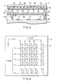
- FIG. 2 is a sectional view for explaining an internal structure of the display unit of FIG. 1;
- FIG. 3 is a partially enlarged sectional view of FIG. 2;
- FIG. 4 is a conceptual illustration of an electron emitter with a number of electron emission elements arranged on a rear substrate of the display unit of FIG. 1;
- FIG. 5 is a diagrammatic plan view showing an electron emission element according to an embodiment of the invention;
- FIG. 6 is a flowchart for explaining a method of manufacturing the electron emission element of FIG. 5;
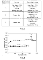
- FIG. 7 is a table showing processing conditions when eliminating impurities from three electron emission elements; and
- FIG. 8 is a graph showing changes in an emission current when driving an electron emission element manufactured under the processing conditions of FIG. 7 for a long time.
- Embodiments of the invention will be explained in detail hereinafter with reference to the accompanying drawings.
- FIG. 1 shows an external perspective view of SED (Surface-conduction Electron-emitter Display) having a number of surface-conduction electron emission elements, as a display unit according to an embodiment of the invention.
- The SED has a rectangular rear plate 10 (a substrate, a rear substrate) and a face plate 12 (a front substrate), which are made of quartz. These
plates rear plate 10 andface plate 12 are joined in the peripheral edge portions through a rectangular frame-like sidewall 14 made of glass, forming a flatrectangular vacuum enclosure 15. - As shown in FIG. 2 and FIG. 3, a fluorescent screen 16 is formed on the inner surface (opposite side) of the
face plate 12. The fluorescent screen 16 is configured by red, blue and greenfluorescent layers 16a and blackcolored layers 16b placed between the fluorescent layers. Thesefluorescent layers 16a are formed like a stripe or a dot. Ametal back 17 made of aluminum, for example, is formed on the fluorescent screen 16. A transparent conductive layer or a color filter film made of ITO may be provided between theface plate 12 and fluorescent screen 16. A structure with several layers stacked on theface plate 12 as described above serves as an image display unit of the invention. - On the inner surface (opposite side) of the
rear plate 10, there is provided a number of surface-conductionelectron emission elements 18 to emit an electron beam for exciting and lighting thefluorescent layer 16a. Theseelectron emission elements 18 are provided 1:1 to each pixel, that is, eachfluorescent layer 16a, and arranged in columns and rows. Each of theelectron emission elements 18 will be described in detail later. - As shown in FIG. 4, a number of wires to connect the
electron emission elements 18 are provided like a matrix on therear plate 10. A structure with a number ofelectron emission elements 18 wired and arranged as a matrix on therear plate 10 serves as an electron emitter of the invention. Various patterns may be used for arranging theelectron emission elements 18. Here, one example will be explained with reference to FIG. 4. - An electron emitter is configured by arranging a number of
electron emission elements 18 on the inner surface of therear plate 10. Namely, theelectron emission elements 18 are formed in m number in the X (vertical) direction in the drawing, and n number in the Y (horizontal) direction. - One of the electrodes of each
electron emission element 18 is connected with a wire common to theelectron emission elements 18 arranged on the same line. This is called a Y wiring. The Y wiring consists of m number of wires from Y1 to Ym. The other one of the electrodes of eachelectron emission element 18 is connected with a wire common to theelectron emission elements 18 arranged on the same line. This is called an X wiring. The X wiring consists of n number of wires from X1 to Xn. - The X and Y wirings are formed by the same method of film forming and patterning, by using the same material as a pair of electrode films of each
electron emission element 18 to be described later. There is an intersection between the X and Y wirings. The intersection is assumed to be electrically insulated by a not-shown insulating film. As an insulating film, there is SiO2 formed by vacuum evaporation, printing or spattering, for example. - The Y wiring is to be supplied with a signal voltage (a scan signal) for selecting a line of the
electron emission elements 18 arranged in the Y direction, and the X wiring is to be supplied with a signal voltage (a modulation signal) for modulating the current of theelectron emission elements 18 arranged in the X direction. Therefore, a driving voltage applied to eachelectron emission element 18 is supplied as a difference voltage between the scan signal and modulation signal applied to eachelectron emission element 18. - For example, if a negative threshold voltage Vf [V] is applied to the Y wiring and 0[V] is applied to the X wiring in a specific one of the
electron emission elements 18, a threshold voltage Vf will be applied between the electrodes of the element. - Therefore, by applying a negative threshold voltage Vf [V] (inputting a scan signal) to the wiring Y1 and an optional voltage over 0[V] (a modulation signal) to the wiring X2 - Xn, for example, an element current is not emitted in the
electron emission element 18 connected to the wirings Y1 and X1 (the upper-left element in the drawing), and an optional element current is emitted in the otherelectron emission elements 18. - As described above, in the electron emitter of the above configuration, a specific
electron emission element 18 can be independently selected and driven by using a simple matrix wiring. - The
sidewall 14 joining the peripheral edge portions of theface plate 12 andrear plate 10 configured as described above is sealed to the peripheral edge portions of therear plate 10 andface plate 12, by using a sealingmaterial 20, such as low-melting glass or metals, for joining theface plate 12 andrear plate 10. - The SED also has a
spacer assembly 22 provided between therear plate 10 andface plate 12. Thespacer assembly 22 consists of a plate-like grid 24 and a plurality of column-like spacer 30 set up integrally on both sides of the grid. - More specifically, the
grid 24 has afirst side 24a opposed to the inner surface of theface plate 12, and asecond side 24b opposed to the inner surface of therear plate 10, and is arranged parallel to theseplates grid 24 has a number of beam-passingholes 26 and a plurality ofspacer hole 28, which are formed by etching, for example. The beam-passingholes 26 are arranged opposite to theelectron emission elements 18, and the spacer holes 28 are arranged between the beam-passing holes with a predetermined pitch. - The
grid 24 is made of am iron-nickel based metal plate in thickness of 0.1 - 0.25 [mm]. The surface of the grid is formed with a film oxide made of Fe3O4 of NiFe3O4, for example. The beam-passinghole 26 is formed like a rectangle of 0.15 - 0.25 [mm] × 0.20 - 0.40 [mm]. Thespacer hole 28 is formed like a circle with a diameter of 0.1 - 0.2 [mm]. - On the
first side 24a of thegrid 24, afirst spacer 30a is set up integrally over eachspacer hole 28, and its extended end contacts the inner surface of theface plate 12 through the metal back 17 and the blackcolored layer 16b of the fluorescent screen 16. On thesecond side 24b of thegrid 24, asecond spacer 30b is set up integrally over eachspacer hole 28, and its extended end contacts the inner surface of therear plate 10. Thespacer hole 28 and the first andsecond spacers second spacers spacer hole 28. - Each of the first and
second spacers grid 24 toward the extended end, more specifically, like a truncated cone. - For example, the
first spacer 30a is formed, so that the diameter at the end portion close to thegrid 24 is approximately 400 [µm], the diameter of the end portion close to the extended end is approximately 280 [µm], and the height is 0.3 - 0.5 [mm]. The aspect ratio (height/diameter of the end close to the grid) is 0.75 - 1.25. - The
second spacer 30b is formed, so that the diameter at the end portion close to thegrid 24 is approximately 400 [µm], the diameter of the end portion close to the extended end is approximately 150 [µm], and the height is 1 - 1.2 [mm]. The aspect ratio is 2.5 - 3. - As described before, the diameter of the
spacer hole 28 formed in thegrid 24 is 0.1 - 0.2 [mm], and set to be enough smaller than the diameter of the end portion of thefirst spacer 30a close to the grid and the diameter of thesecond spacer 30b close to the grid. As thefirst spacer 30a andsecond spacer 30b are aligned integrally and coaxially with thespacer hole 28, the first and second spacers are connected integrally with each other through thespacer hole 28, and configured integrally with thegrid 24. - The
grid 24 of thespacer assembly 22 configured as above is supplied with a predetermined voltage from a not-shown power supply, preventing a crosstalk, and converges an electron beam emitted from the correspondingelectron emission element 18 on a desired fluorescent layer through the beam-passinghole 26. The first andsecond spacers face plate 12 andrear plate 10, supports an atmospheric load acting on theplates vacuum enclosure 15, and keeps an interval between the plates at a predetermined value. - When manufacturing a SED by incorporating the
spacer assembly 22 produced as above, prepare therear plate 10 provided with theelectron emission elements 18 and joined with thesidewall 14, and theface plate 12 provided with the fluorescent screen 16 and metal back 17. Place therear plate 10 andface plate 12 in a not-shown vacuum chamber, in the state that thespacer assembly 22 produced as above is positioned on therear plate 10. Vacuum exhaust the vacuum chamber, and join theface plate 12 with therear plate 10 through thesidewall 14. A SED having thespacer assembly 22 is manufactured in this way. - Next, the
electron emission element 18 will be explained in details with reference to FIG. 5. FIG. 5 is a schematic plan of oneelectron emission element 18 viewed from the inner surface of therear plate 10. - The
electron emission element 18 is formed on the inner surface of therear plate 10, consisting of two (a pair of)element electrodes conductive film 34 connecting the gap between theelement electrodes electron emitter 36 shaped as a line just like dividing theconductive film 34. - As a material of the
rear plate 10, glass with decreased impurities, such as Na, a blue plate glass, a laminate with SiO2 laminated on a blue glass by spattering, ceramics such as alumina, and a Si substrate may be used, as well as a quarts glass adopted in this embodiment. - As a material of the
element electrodes element electrodes - Each of the
element electrodes - As a material of the
conductive film 34, there are metals such as Pd, Pt, Ru Ag, Au, Ti, In, Cu, Cr, Fe, Zn, Sn, Ta, W and Pb, oxide conductors such as PdO, SnO2, In2O3, PbO and Sb2O3, silicides such as HfB2, ZrB2, LaB6, CeB6, YB4 and GdB4, carbides such as TiC, ZrC, HfC, TaC, SiC and WC, nitrides such as TiN, ZrN and HfN, semiconductors such as Si and Ge, and carbon. In this embodiment, Pd is formed by spattering and heated by oxidation in the air, and then theconductive film 34 with the width of 50 [µm] and length of 40 [µm] is formed by photolithography or dry etching. - The
electron emitter 36 consists of a high-resistance crack formed in a part of theconductive film 34, and depends on the thickness, quality and material of theconductive film 34 and the technique such as electrical forming to be described later. - Fine conductive particle with a diameter of several Å to several tens nm may exist inside the
electron emitter 36. This fine conductive particle contains a part or all elements of a material forming theconductive film 34. Carbon or carbon oxide is deposited at least in theelectron emitter 36 and on theconductive film 34 close to the electron emitter. - Next, an explanation will be given on a method of manufacturing the
electron emission element 18 with the structure described above with reference to a flowchart of FIG. 6. - First, clean the
rear plate 10 sufficiently with an organic solvent, and form a Pt film as a material of theelement electrodes square element electrodes rear plate 10 by photolithography (step 1). - Next, apply an organic metal solvent to the
rear plate 10 provided with the pairs ofelement electrodes - Further, make a forming process for forming the
electron emitter 36 on each conductive film 34 (step 3). The forming process is performed usually by giving a potential difference to a pair ofelement electrodes conductive film 34. - Namely, by placing a voltage between the
element electrodes conductive film 34, a crack is generated in theconductive film 34, and theelectron emitter 36 is formed. A pulse wave voltage is desirable for the forming process. Measure a current caused by application of a voltage of approximately 0.1V, for example, and obtain a resistance value. When the resistance value over 1 MΩ is obtained, finish the forming process. - In this embodiment, the
rear plate 10 formed with theelement electrodes 31/32 andconductive film 34 is placed in a vacuum unit, and a voltage is placed between theelectrode elements element electrodes electron emitter 36 is formed at substantially the midpoint position of theconductive film 34. - After the above forming process, the
electron emission element 18 is subjected to an activation process (step 4). The activation process is performed by placing a pulse-like voltage between theelement electrodes - The atmosphere containing an organic substance gas can be formed by utilizing an organic gas remained in an atmosphere after exhausting the vacuum unit by using an oil diffusion pump or a rotary pump, or by leading an appropriate organic substance gas into a vacuum. As an appropriate organic substance, there are aliphatic hydrocarbons, aromatic hydrocarbons, alcohol, aldehyde, ketone, amine, organic acid, etc.
- In this embodiment, methane on the order of 10-3 [Pa] is introduced into the vacuum unit provided with the
rear plate 10, and activation is performed. The voltage applied to theelement electrodes - By this activation, carbon or carbon compound of an organic substance existing in the atmosphere is deposited on the
electron emission element 18, and at least theelectron emitter 36 is carbonized. This extremely increases the element current If and emission current Ie. The film thickness of the deposit is preferably under 50 [nm], more preferably under 30 [nm]. - The
electron emission element 18 activated as described above is subject to a heating (baking) process in a vacuum atmosphere (step 5). In other words, therear plate 10 placed in a vacuum unit is heated, and an organic gas remained in a vacuum unit is exhausted. A vacuum exhaust unit to exhaust a vacuum unit is preferably a unit not using oil, so that oil generated from the unit does not affect the characteristics of theelectron emission element 18. A partial pressure of an organic component in a vacuum unit is preferably lower than 10-6 [Pa], at which the above carbon or carbon compound is almost not deposited, more preferably lower than 10-8 [Pa]. Further, when exhausting a vacuum unit, heat the whole vacuum unit to facilitate exhaustion of organic substance molecules adhered to the inner wall of a vacuum unit orelectron emission element 18. - After the above baking process, perform an impurities eliminating process to more securely eliminate impurities causing degradation of the characteristics of the electron emission element 18 (step 6). In this time, a voltage of the same polarity as ordinary driving (a positive polarity in this embodiment) is given in a vacuum atmosphere to the
element electrodes electron emission element 18 on therear plate 10 placed in the vacuum unit, and the element electrodes are pre-driven at the appropriate times. In the pre-driving, a voltage of the same direction and higher than that as ordinary operation is given to theelement electrodes element electrodes - Namely, in the impurities elimination process, the impurities are eliminated from the
electron emitter 36 by giving theelement electrodes 31 and 32 a voltage of the same polarity as that in ordinary operation for a predetermined time, and then giving a voltage of the polarity opposite to that in ordinary operation for a predetermined time. More concretely, the impurities adhered to the electron emitter surface of the "+" electrode side are eliminated by making theelectron emitter 36 emit an electron by giving a positive polarity voltage to theelement electrodes electron emitter 36 emit an electron by giving a negative polarity voltage to theelement electrodes - In this embodiment, the impurities adhered to the surface of the
electron emitter 36 are eliminated by giving positive and negative polarity pulse voltages alternately to theelement electrodes electron emission element 18 is detected through a not-shown detector, the emission current is monitored, application of power to theelement electrodes element electrodes - As a pulse voltage waveform, various waveforms such as square, sinusoidal and triangular waves may be used. As a pulse voltage polarity, positive polarity, negative polarity, and alternate positive-negative polarity may be used. Namely, the largeness, pulse width, frequency, polarity and waveform of the pulse voltage may be appropriately adjusted. Power may be continuously applied, until the impurities adhered to the
electron emitter 36 of theelectron emission element 18 are completely eliminated. - As described hereinbefore, according to this embodiment, it is possible to securely eliminate the impurities adhered to the
electron emitter 36 of theelectron emission element 18 by a simple method of applying a voltage of the polarity opposite to that in ordinary operation to theelement electrodes electron emission element 18, without using an exclusive processor for eliminating impurities. Therefore, the characteristics of theelectron emission element 18 can be stabilized for a long period of time. - In order to verify the effect of the invention, the inventor performed an impurities elimination process for three electron emission elements A, B and C under different conditions. FIG. 7 shows the processing conditions for the electron emission elements A, B and C. FIG. 8 graphically shows changes in an emission current when the electron emission elements A, B and C are driven for a long time (1400 hours in the embodiment) after the processing. For comparison purposes, FIG. 8 shows changes in an emission current when an electron emission element not subject to the electron cleaning process of FIG. 7 is driven for a long time. A voltage given to the
element electrodes - For the electron emission element A, a pulse voltage is given to the
element electrodes element electrodes electron elements electron elements - As shown in FIG. 8, the emission current is almost not changed and stable even after a SED having three electron emission elements A, B and C is driven for 1400 hours. Contrarily, the emission current rises with the passage of time in the example not subjected to the electron cleaning process. Namely, in the electron emission element of the example, the adhered impurities affected by gas during the manufacturing process are not completely eliminated, and the emission current is increased by emission of the gas adhered to the surface of the electron emission element by the heat generated by driving.
- The invention is not to be limited to the embodiment described above. The invention may be embodied by modifying the components without departing from its essential characteristics. The invention may be embodied in other specific forms by appropriately combining the constituent elements disclosed in the aforementioned embodiment. For example, some of the components shown with the embodiment may be deleted.
- For example, in the aforementioned embodiment, the impurities elimination process is performed after the baking process and before the sealing process. But, the impurities may be eliminated during or before the baking process, or after the activation process.
- In the aforementioned embodiment, the impurities elimination process is performed during the SED manufacturing process. But, the impurities elimination process may be performed after the SED is manufactured, by opposing the
rear plate 10 andface plate 12 and sealing their peripheral edges. In this case, while driving the SED, monitor the emission current emitted from theelectron emission element 18 through a not-shown detector, and eliminate the impurities by using the cleaning function when the emission current value (the amount of emitted electron) changes over a preset value. Namely, according to the invention, the impurities elimination process can be performed at a desired timing during or after manufacturing SED. Therefore, changes with time of the emission current value of theelectron emission element 18 of SED can be eliminated, and stable driving characteristics can be obtained for a long period of time. - As explained hereinbefore, according to the invention, impurities causing degradation of characteristics of an electron emission element can be securely eliminated by a simple method. An electron emission element can be cleaned at a desired timing after manufacturing a display unit, and degradation of characteristics with time caused by adhesion of impurities can be prevented.
Claims (18)
- A method of manufacturing an electron emission element, characterized by comprising:a step of forming a pair of electrodes spaced on a substrate;a step of forming a conductive film to connect the pair of electrodes;a step of forming an electron emitter on the conductive film; anda step of eliminating impurities from the electron emitter, by making the electron emitter emit an electron by applying a voltage to the pair of electrodes, and by making the electron emitter emit an electron by applying a reverse polarity voltage to the pair of electrodes.
- The method of manufacturing an electron emission element according to claim 1, characterized by further comprising a step of activation to carbonize the electron emitter after the step of forming an electron emitter and before the step of eliminating impurities.
- The method of manufacturing an electron emission element according to claim 2, characterized by further comprising a step of baking for a heating process in a vacuum atmosphere after the step of activation and before the step of eliminating impurities.
- A method of manufacturing an electron emission element, characterized by comprising:a step of forming a pair of electrodes spaced on a substrate;a step of forming a conductive film to connect the pair of electrodes;a step of forming an electron emitter on the conductive film;a step of pre-driving to make the electron emitter emit an electron by applying a voltage to the pair of electrodes; anda step of eliminating impurities from the electron emitter, by making the electron emitter emit an electron by applying a voltage of polarity opposite to that in the step of pre-driving.
- The method of manufacturing an electron emission element according to claim 4, characterized by further comprising a step of activation to carbonize the electron emitter after the step of forming an electron emitter and before the step of pre-driving.
- The method of manufacturing an electron emission element according to claim 5, characterized by further comprising a step of baking for a heating process in a vacuum atmosphere after the step of activation and before the step of pre-driving.
- The method of manufacturing an electron emission element according to claim 1 or 4,
characterized in that a voltage applied to the pair of electrodes is a pulse voltage of any one of square, sinusoidal and triangular waves. - The method of manufacturing an electron emission element according to claim 7, characterized in that the pulse voltage includes at least one of positive polarity voltage pulse and negative polarity voltage pulse.
- The method of manufacturing an electron emission element according to claim 7, characterized in that the step of eliminating impurities has:a step of detecting an electron emitted from the electron emitter; anda step of adjusting at least one of largeness, pulse width, frequency and polarity of a voltage applied to the pair of electrodes, based on the result of detection in the step of detection.
- A method of manufacturing a display unit, characterized by comprising:a step of forming pairs of electrodes on a substrate;a step of forming conductive films to connect the pairs of electrodes;a step of forming an electron emitter on each of the conductive films;a step of activation to carbonize at least the electron emitters;a step of baking for heating the rear substrate in a vacuum atmosphere;a step of eliminating impurities from the electron emitters, by making the electron emitters emit an electron by applying a voltage to the pairs of electrodes, and by making the electron emitters emit an electron by applying a reverse polarity voltage to the pairs of electrodes; anda step of sealing for combining a front substrate having a fluorescent layer and the rear substrate in a vacuum atmosphere, and sealing peripheral edges of the substrates.
- The method of manufacturing a display unit according to claim 10, characterized in that the step of eliminating impurities is performed during or before the step of baking.
- The method of manufacturing a display unit according to claim 11, characterized in that the step of eliminating impurities is performed after the step of activation.
- The method of manufacturing a display unit according to claim 10, characterized in that the step of eliminating impurities is performed after the step of sealing.
- The method of manufacturing a display unit according to any one of claims 10 - 13, characterized in that a voltage applied to the pairs of electrodes is a pulse voltage of any one of square, sinusoidal and triangular waves.
- The method of manufacturing a display unit according to claim 14, characterized in that the pulse voltage includes at least one of positive polarity voltage pulse and negative polarity voltage pulse.
- The method of manufacturing a display unit according to claim 14, characterized in that the step of eliminating impurities has:a step of detecting en electron emitted from the electron emitters; anda step of adjusting at least one of largeness, pulse width, frequency and polarity of a voltage applied to the pairs of electrodes, based on the result of detection in the step of detection.
- A display unit characterized by comprising:a rear substrate and a front substrate which are opposed to each other through a predetermined clearance;electron emission elements which are provided on the opposite side of the rear substrate, and selectively emit an electron by giving pairs of electrodes a voltage corresponding to an image signal; andan image display which is provided on the opposite side of the front substrate, and displays an image by collision of electrons;the display unit having a cleaning function for cleaning impurities close to the electron emitters, by making the electron emission elements emit an electron by giving the pairs of electrodes a voltage of the same polarity as when displaying an image, and by making the electron emission elements emit an electron by giving the pairs of electrodes a reverse polarity voltage.
- The display unit according to claim 17, characterized by further comprising:a detector for monitoring an electron emitted from the electron emitters while displaying an image,wherein when the amount of electron monitored by the detector changes over a predetermined value, the cleaning function for eliminating impurities by giving positive and reverse polarity voltages alternately to the pairs of electrodes is operated.
Applications Claiming Priority (1)
| Application Number | Priority Date | Filing Date | Title |
|---|---|---|---|
| PCT/JP2004/013761 WO2006033137A1 (en) | 2004-09-21 | 2004-09-21 | Electron emitting element manufacturing method, displayer manufacturing method and displayer provided with electron emitting element cleaning function |
Publications (1)
| Publication Number | Publication Date |
|---|---|
| EP1793405A1 true EP1793405A1 (en) | 2007-06-06 |
Family
ID=36089904
Family Applications (1)
| Application Number | Title | Priority Date | Filing Date |
|---|---|---|---|
| EP04787944A Withdrawn EP1793405A1 (en) | 2004-09-21 | 2004-09-21 | Electron emitting element manufacturing method, displayer manufacturing method and displayer provided with electron emitting element cleaning function |
Country Status (2)
| Country | Link |
|---|---|
| EP (1) | EP1793405A1 (en) |
| WO (1) | WO2006033137A1 (en) |
Family Cites Families (3)
| Publication number | Priority date | Publication date | Assignee | Title |
|---|---|---|---|---|
| JP2000243293A (en) * | 1999-02-24 | 2000-09-08 | Canon Inc | Electron source manufacturing apparatus, electron source manufacturing method and electron source |
| JP3437519B2 (en) * | 1999-02-25 | 2003-08-18 | キヤノン株式会社 | Manufacturing method and adjustment method of electron-emitting device |
| JP3733308B2 (en) * | 2000-09-29 | 2006-01-11 | キヤノン株式会社 | Manufacturing method of image display device |
-
2004
- 2004-09-21 WO PCT/JP2004/013761 patent/WO2006033137A1/en not_active Ceased
- 2004-09-21 EP EP04787944A patent/EP1793405A1/en not_active Withdrawn
Non-Patent Citations (1)
| Title |
|---|
| See references of WO2006033137A1 * |
Also Published As
| Publication number | Publication date |
|---|---|
| WO2006033137A1 (en) | 2006-03-30 |
Similar Documents
| Publication | Publication Date | Title |
|---|---|---|
| EP0836213B1 (en) | Image-forming apparatus | |
| EP0986085B1 (en) | Method for manufacturing cathode, electron source, and image forming apparatus | |
| US7582002B2 (en) | Manufacturing method of electron emitting device, electron source and image display apparatus | |
| KR100229232B1 (en) | Electron emitting devices, electron source substrates, electron sources, display panels and image forming apparatuses, and methods of manufacturing the same | |
| JPH10326583A (en) | Electron emission device, image forming device and voltage application device using the same | |
| KR100709173B1 (en) | Image display apparatus and method for manufacturing the same | |
| KR19990088012A (en) | Method of fabricating electron source and image forming apparatus | |
| KR100395602B1 (en) | Manufacture method for electron-emitting device, electron source, and image-forming apparatus | |
| US20070138957A1 (en) | Electron emission element manufacturing method, display unit manufacturing method, and display unit with electron emission element cleaning function | |
| JP2001325904A (en) | Electron emission device, image forming device and voltage application device using the same | |
| KR100934167B1 (en) | Electron-emitting device and image display device | |
| JP3740296B2 (en) | Image forming apparatus | |
| JP2004055347A (en) | Electron-emitting device, electron-emitting device, display device, and method of manufacturing electron-emitting device | |
| WO2006033137A1 (en) | Electron emitting element manufacturing method, displayer manufacturing method and displayer provided with electron emitting element cleaning function | |
| JP2005038619A (en) | Method for manufacturing electron-emitting device, and method for manufacturing display device including the electron-emitting device | |
| JP2005174864A (en) | ELECTRON EMITTING ELEMENT, ELECTRON EMITTING DEVICE, DISPLAY DEVICE, AND METHOD FOR MANUFACTURING ELECTRON EMITTING ELEMENT | |
| JP3571915B2 (en) | Method for manufacturing electron-emitting device | |
| JP2004063103A (en) | Electron-emitting device, electron-emitting device, display device, and method of manufacturing electron-emitting device | |
| JP3938185B2 (en) | Image display device and manufacturing method thereof | |
| JP2005243436A (en) | ELECTRON EMITTING ELEMENT, ELECTRON EMITTING DEVICE, AND DISPLAY DEVICE | |
| JPH11233006A (en) | Method of manufacturing electron source and image forming apparatus | |
| JPH1125849A (en) | Electron emitting element, electron source, and method of manufacturing image forming apparatus | |
| JPH087794A (en) | Image forming device | |
| JPH09231920A (en) | Electron generator and image display device using the same | |
| JP2006134592A (en) | Electron emitting device, electron source, and manufacturing method of image forming apparatus |
Legal Events
| Date | Code | Title | Description |
|---|---|---|---|
| PUAI | Public reference made under article 153(3) epc to a published international application that has entered the european phase |
Free format text: ORIGINAL CODE: 0009012 |
|
| 17P | Request for examination filed |
Effective date: 20070221 |
|
| AK | Designated contracting states |
Kind code of ref document: A1 Designated state(s): DE FR GB IT NL |
|
| DAX | Request for extension of the european patent (deleted) | ||
| RBV | Designated contracting states (corrected) |
Designated state(s): DE FR GB IT NL |
|
| STAA | Information on the status of an ep patent application or granted ep patent |
Free format text: STATUS: THE APPLICATION HAS BEEN WITHDRAWN |
|
| 18W | Application withdrawn |
Effective date: 20080225 |