EP1791156A2 - Plasma display apparatus and method of manufacturing the same - Google Patents
Plasma display apparatus and method of manufacturing the same Download PDFInfo
- Publication number
- EP1791156A2 EP1791156A2 EP06255992A EP06255992A EP1791156A2 EP 1791156 A2 EP1791156 A2 EP 1791156A2 EP 06255992 A EP06255992 A EP 06255992A EP 06255992 A EP06255992 A EP 06255992A EP 1791156 A2 EP1791156 A2 EP 1791156A2
- Authority
- EP
- European Patent Office
- Prior art keywords
- electron emitting
- emitting layers
- sustain electrodes
- display apparatus
- plasma display
- Prior art date
- Legal status (The legal status is an assumption and is not a legal conclusion. Google has not performed a legal analysis and makes no representation as to the accuracy of the status listed.)
- Withdrawn
Links
Images






Classifications
-
- H—ELECTRICITY
- H01—ELECTRIC ELEMENTS
- H01J—ELECTRIC DISCHARGE TUBES OR DISCHARGE LAMPS
- H01J11/00—Gas-filled discharge tubes with alternating current induction of the discharge, e.g. alternating current plasma display panels [AC-PDP]; Gas-filled discharge tubes without any main electrode inside the vessel; Gas-filled discharge tubes with at least one main electrode outside the vessel
- H01J11/20—Constructional details
- H01J11/34—Vessels, containers or parts thereof, e.g. substrates
- H01J11/40—Layers for protecting or enhancing the electron emission, e.g. MgO layers
-
- H—ELECTRICITY
- H01—ELECTRIC ELEMENTS
- H01J—ELECTRIC DISCHARGE TUBES OR DISCHARGE LAMPS
- H01J11/00—Gas-filled discharge tubes with alternating current induction of the discharge, e.g. alternating current plasma display panels [AC-PDP]; Gas-filled discharge tubes without any main electrode inside the vessel; Gas-filled discharge tubes with at least one main electrode outside the vessel
- H01J11/20—Constructional details
- H01J11/22—Electrodes, e.g. special shape, material or configuration
-
- H—ELECTRICITY
- H01—ELECTRIC ELEMENTS
- H01J—ELECTRIC DISCHARGE TUBES OR DISCHARGE LAMPS
- H01J11/00—Gas-filled discharge tubes with alternating current induction of the discharge, e.g. alternating current plasma display panels [AC-PDP]; Gas-filled discharge tubes without any main electrode inside the vessel; Gas-filled discharge tubes with at least one main electrode outside the vessel
- H01J11/20—Constructional details
- H01J11/22—Electrodes, e.g. special shape, material or configuration
- H01J11/28—Auxiliary electrodes, e.g. priming electrodes or trigger electrodes
-
- H—ELECTRICITY
- H01—ELECTRIC ELEMENTS
- H01J—ELECTRIC DISCHARGE TUBES OR DISCHARGE LAMPS
- H01J11/00—Gas-filled discharge tubes with alternating current induction of the discharge, e.g. alternating current plasma display panels [AC-PDP]; Gas-filled discharge tubes without any main electrode inside the vessel; Gas-filled discharge tubes with at least one main electrode outside the vessel
- H01J11/20—Constructional details
- H01J11/34—Vessels, containers or parts thereof, e.g. substrates
-
- H—ELECTRICITY
- H01—ELECTRIC ELEMENTS
- H01J—ELECTRIC DISCHARGE TUBES OR DISCHARGE LAMPS
- H01J9/00—Apparatus or processes specially adapted for the manufacture, installation, removal, maintenance of electric discharge tubes, discharge lamps, or parts thereof; Recovery of material from discharge tubes or lamps
- H01J9/02—Manufacture of electrodes or electrode systems
-
- H—ELECTRICITY
- H01—ELECTRIC ELEMENTS
- H01J—ELECTRIC DISCHARGE TUBES OR DISCHARGE LAMPS
- H01J2211/00—Plasma display panels with alternate current induction of the discharge, e.g. AC-PDPs
- H01J2211/20—Constructional details
- H01J2211/22—Electrodes
- H01J2211/225—Material of electrodes
Definitions
- the present present invention relates to a plasma display apparatus, and more particularly, to a plasma display apparatus having an improved structure so as to increase luminescence efficiency and uniformity and a method of manufacturing the plasma display apparatus.
- Plasma display panels form images using electrical discharge, have good brightness characteristics and a wide viewing angle, etc., leading to an increase in the use of PDPs recently.
- PDPs display images using visible light emitted through a process of exciting a phosphor material with ultraviolet rays generated from a discharge of a discharge gas between electrodes when a direct current (DC) voltage or an alternating current (AC) voltage is applied to the electrodes.
- DC direct current
- AC alternating current
- PDPs are classified into DC type panels and AC type panels according to the discharge process (the discharge method).
- PDPs are classified into facing discharge type panels and surface discharge type panels according to the arrangement of electrodes.
- FIG. 1 is an exploded perspective view of a conventional plasma display panel (PDP).
- PDP plasma display panel
- the conventional PDP includes a rear substrate 10 and a front substrate 20, which face each other, and a plurality of barrier ribs 13 interposed between the rear substrate 10 and the front substrate 20 form discharge spaces 15 which are filled with a discharge gas such as Xenon Xe.
- the barrier ribs 13 partition a plurality of unit discharge cells and prevent electrical and optical crosstalk between the unit discharge cells.
- the rear substrate 10 includes address electrodes 11 that are covered by a first dielectric layer 12 that is coated with phosphor layers 14 including red R, green G, and blue B phosphor layers.
- the front substrate 20 includes first and second sustain electrodes 21 a and 21b on which first and second bus electrodes 22a and 22b are formed, respectively, to reduce line resistance of the first and second sustain electrodes 21a and 21b.
- a second dielectric layer 23 covers the first and second sustain electrodes 21a and 21b and the first and second bus electrodes 22a and 22b.
- a protective layer 24 formed of MgO is formed on the second dielectric layer 23. The protective layer 24 prevents the second dielectric layer 23 from being damaged due to plasma sputtering, emits secondary electrons during a plasma discharge, and reduces a discharge voltage.
- the conventional PDP illustrated in FIG. 1 continuously supplies and accelerates electrons through a discharge, generates excitation particles due to collisions of the accelerated electrons and neutral particles, emits ultraviolet rays owing to the stabilization of the excitation particles, excites a phosphor substance by incidence of the ultraviolet rays to form visible light, emits the visible light through the front substrate 20, and displays images.
- the density of electron emission contributing to the discharge is not constant in the unit discharge cells, thus reducing luminescence uniformity of the conventional PDP illustrated in FIG. 1.
- the current density is high inside the first and second sustain electrodes 21a and 21b, resulting in a strong luminescence, and the current density is low outside the first and second sustain electrodes 21a and 21b, resulting in a weak luminescence. That is, an electric field of the unit discharge cells is not constant so that areas having strong luminescence and weak luminescence coexist.
- the conventional PDP has a high discharge voltage and a low discharge or luminescence efficiency. Therefore, it is necessary to improve the structure of the PDP so as to increase the luminescence efficiency and uniformity.
- the present invention sets out to provide a plasma display apparatus having an improved structure so as to increase luminescence efficiency and uniformity and a method of manufacturing the plasma display apparatus.
- a plasma display apparatus as set out in Claim 1 or Claim 8.
- Preferred features of this aspect of the invention are set out in Claims 2 to 7 and 9 to 13.
- a second aspect of the invention provides a method of manufacturing a plasma display apparatus as set out in Claim 14 or Claim 18. Preferred features of this aspect of the invention are set out in Claims 15 to 17 and 19 to 21.
- FIG. 1 is an exploded perspective view of a conventional plasma display panel (PDP);
- PDP plasma display panel
- FIG. 2A is an exploded perspective view of a plasma display apparatus according to an embodiment of the invention.
- FIG. 2B is a cross-sectional view of the plasma display apparatus of FIG. 2A taken along a line A-A' in FIG. 2A;
- FIG. 3A is an exploded perspective view of a plasma display apparatus according to another embodiment of the invention.
- FIG. 3B is a cross-sectional view of the plasma display apparatus of FIG. 3A taken along a line B-B' in FIG. 3A;
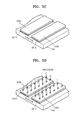
- FIGS. 4A through 4H are diagrams illustrating a method of manufacturing a plasma display apparatus, according to an embodiment of the invention.
- FIGS. 5A through 5I are diagrams illustrating a method of manufacturing a plasma display apparatus, according to another embodiment of the invention.
- FIG. 2A is an exploded perspective view of a plasma display apparatus according to an embodiment.
- FIG. 2B is a cross-sectional view of the plasma display apparatus of FIG. 2A taken along a line A-a' in FIG. 2A.
- a plasma display panel (PDP) is realized as an example of the plasma display apparatus according to the current embodiment.
- the plasma display apparatus includes a front substrate 120 and a rear substrate 110 which face each other, and a plurality of barrier ribs 113 interposed between the front substrate 120 and the rear substrate 110, forming discharge spaces 115 filled with a discharge gas such as, for example, Neon Ne or Xenon Xe.
- the barrier ribs 113 partition a plurality of unit discharge cells.
- the discharge gas generates a visible light in the unit discharge cells during a plasma discharge.
- the barrier ribs 113 prevent electrical or optical crosstalk between the unit discharge cells.
- the rear substrate 110 includes address electrodes 111 and a first dielectric layer 112 that covers the address electrodes 111.
- the first dielectric layer 112 is coated with phosphor layers 114 including red R, green G, and blue B phosphor layers.
- the front substrate 120 includes first and second sustain electrodes 121 a and 121b which are spaced apart from each other.
- a second dielectric layer 123 covers the first and second sustain electrodes 121a and 121b.
- First and second emitter electrodes 124a and 124b formed of conductive materials such as indium tin oxide (ITO), Al, Ag, etc. are formed on the second dielectric layer 123, and correspond to the first and second sustain electrodes 121a and 121b, respectively.
- First and second electron emitting layers 128a and 128b formed of an oxidized porous silicon (OPS) material are formed on the first and second emitter electrodes 124a and 124b, respectively.
- the OPS material is an oxidized porous polysilicon (OPPS) or an oxidized porous amorphous silicon (OPAS).
- first and second sustain electrodes 121a and 121b If a specific alternating current (AC) voltage is applied to the first and second sustain electrodes 121a and 121b, an electric field having a specific magnitude is formed between the first and second sustain electrodes 121a and 121b so that the first and second emitter electrodes 124a and 124b supply electrons to the first and second electron emitting layers 128a and 128b, respectively.
- the electrons are accelerated through the first and second emitting layers 128a and 128b and emitted to the discharge spaces 115. More specifically, silicon nano-crystallization particles forming the first and second electron emitting layers 128a and 128b have a diameter of about 5 nm.
- the diameter of the silicon nano-crystallization particles is much smaller than a means free path of about 50 nm of the electrons. Therefore, the electrons are not likely to collide with each other in the silicon nano-crystallization particles, and most of the electrons reach the interface of the silicon nano-crystallization particles through the silicon nano-crystallization particles.
- a very thin oxidization film is formed between the silicon nano-crystallization particles forming an electric field area in the first and second electron emitting layers 128a and 128b when a specific voltage is applied to the first and second sustain electrodes 121a and 121b.
- the electrons tunnel through the oxidization film are accelerated in the electric field area formed in the first and second electron emitting layers 128a and 128b, and are emitted to the discharge spaces 115. Therefore, the first and second electron emitting layers 128a and 128b of the plasma display apparatus according to the current embodiment can improve discharge and brightness characteristics of the plasma display apparatus.
- the first and second emitter electrodes 124a and 124b may have the same structure as the first and second electron emitting layers 128a and 128b. In this case, the density of the electrons emitted from the first and second electron emitting layers 128a and 128b is changed according to the width of the first and second electron emitting layers 128a and 128b.
- the density of the electrons contributing to the discharge is more uniform than the discharge spaces 115.
- the plasma display apparatus of the current embodiment can provide an improved distribution of the electric field in the unit discharge cells compared to the conventional PDP.
- the conventional PDP has a strong luminescence since the current density is high inside the first and second sustain electrodes 21a and 21b, and has a weak luminescence since the current density is low outside the first and second sustain electrodes 21a and 21b.
- the plasma display apparatus of the current embodiment has a weak current density by relatively decreasing the width of the first and second electron emitting layers 128a and 128b inside the first and second sustain electrodes 121a and 121b, and has a strong current density by relatively increasing the width of the first and second electron emitting layers 128a and 128b outside the first and second sustain electrodes 121a and 121b. Therefore, the unit discharge cells have a uniformly distributed electric field, thereby increasing luminescence efficiency and uniformity in the unit discharge cells and improving the voltage and brightness characteristics of the plasma display apparatus.
- FIG. 3A is an exploded perspective view of a plasma display apparatus according to another embodiment of the invention.
- FIG. 3B is a cross-sectional view of the plasma display apparatus of FIG. 3A taken along a line B-B' in FIG. 3A.
- a PDP is realized as an example of the plasma display apparatus according to the current embodiment.
- FIGS. 3A and 3B denote like elements illustrated in FIGS. 2A and 2B, and thus descriptions thereof will be omitted.
- a front substrate 220 of the plasma display apparatus of FIGS. 3A and 3B is different from the front substrate 120 of the plasma display apparatus of FIGS. 2A and 2B.
- the plasma display apparatus includes the front substrate 220 and a rear substrate 110 which face each other, and a plurality of barrier ribs 113 interposed between the front substrate 220 and the rear substrate 110, forming discharge spaces 115 filled with a discharge gas such as Neon Ne or Xenon Xe.
- the barrier ribs 113 partition a plurality of unit discharge cells.
- the rear substrate 110 includes address electrodes 111 and a first dielectric layer 112 that covers the address electrodes 111.
- the first dielectric layer 112 is coated with phosphor layers 114 including red R, green G, and blue B phosphor layers.
- the front substrate 220 includes first and second sustain electrodes 221 a and 221b which are spaced apart from each other.
- First and second electron emitting layers 228a and 228b formed of an OPS material are formed on the first and second sustain electrodes 221a and 221b, respectively.
- a second dielectric layer 229 covers the first and second electron emitting layers 228a and 228b.
- the second dielectric layer 229 includes a window that exposes upper faces of the first and second electron emitting layers 228a and 228b to the discharge spaces 115.
- a density of electrons emitted from the first and second electron emitting layers 228a and 228b is changed according to the width of the window.
- the closer the first and second electron emitting layers 228a and 228b are to the gap between the first and second sustain electrodes 221a and 221b the lower the density of the electrons emitted from the first and second electron emitting layers 228a and 228b is, and vice versa.
- the plasma display apparatus of the current embodiment can increase luminescence efficiency and uniformity in the unit discharge cells and thus improve voltage and brightness characteristics of the plasma display apparatus.
- the first and second sustain electrodes 221a and 221b can be formed of a material selected from the group consisting of ITO, Al, and Ag.
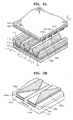
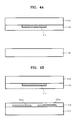
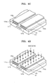
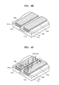
- FIGs. 4A through 4H are diagrams illustrating a method of manufacturing a plasma display apparatus such as shown in Figures 2A and 2B .
- a PDP is realized as an example of the plasma display apparatus according to the current embodiment.
- Material layers can be formed using various widely known thin film deposition methods. Such thin film deposition methods include physical vapor deposition (PVD), chemical vapor deposition (CVD), spray coating, screen printing, etc.
- a front substrate 120 and a rear substrate 110 are prepared facing each other Address electrodes 111 and a first dielectric layer 112 that covers the address electrodes 111 are formed on the rear substrate 110.
- First and second sustain electrodes 121a and 121b formed on the front substrate 120 to be spaced apart from each other, are formed of a conductive material such as ITO, Al, or Ag.
- a second dielectric layer 123 covers the first and second sustain electrodes 121a and 121b .
- first and second emitter electrodes 124a and 124b are formed on the second dielectric layer 123 so as to correspond to the first and second sustain electrodes 121a and 121b, respectively.
- the first and second emitter electrodes 124a and 124b are formed of a conductive material such as ITO, Al, or Ag.
- First and second silicon layers 125a and 125b are formed on the first and second emitter electrodes 124a and 124b, respectively.
- the first and second silicon layers 125a and 125b are formed of a polycrystalline silicon or an amorphous silicon.
- the first and second silicon layers 125a and 125b are anodized to form first and second electron emitting layers 128a and 128b, which are formed of an OPS material.
- Any anodizing process is known in the art can be used.
- a solution of hydrogen fluoride (HF) and ethanol is used for the anodizing process, thereby obtaining an OPS layer.
- a specific area of the first and second electron emitting layers 128a and 128b is etched and removed in order to decrease the width of the first and second electron emitting layers 128a and 128b when the first and second electron emitting layers 128a and 128b are close to a gap between the first and second emitter electrodes 124a and 124b, thereby obtaining a plasma display apparatus having improved luminescence efficiency and uniformity.
- a gap between the first and second electron emitting layers 128a and 128b can influence a discharge start voltage of the plasma display apparatus. Therefore, the gap between the first and second electron emitting layers 128a and 128b may be controlled in order to minimize the discharge start voltage. For example, the gap between the first and second electron emitting layers 128a and 128b can be increased or decreased during the etching process.
- FIGS. 5A through 51 are diagrams illustrating a method of manufacturing a plasma display apparatus such as shown in Figures 3A and 3B.
- a PDP is realized as an example of the plasma display apparatus according to the current embodiment.
- a front substrate 220 and a rear substrate 110 are prepared facing each other.
- Address electrodes 111 and a first dielectric layer 112 that covers the address electrodes 111 are formed on the rear substrate 110.
- First and second sustain electrodes 221a and 221b are formed on the front substrate 220 and spaced apart from each other.
- First and second silicon layers 225a and 225b are formed on the first and second sustain electrodes 221a and 221b, respectively.
- the first and second silicon layers 225a and 225b are formed of a polycrystalline silicon or an amorphous silicon.
- the first and second sustain electrodes 221a and 221b are formed of a conductive material such as ITO, Al, or Ag.
- the first and second silicon layers 225a and 225b are anodized to form first and second electron emitting layers 228a and 228b, which are formed of an OPS material.
- the anodizing process is the same as that described with reference to FIGS. 4A through 4H, and thus a description thereof will be omitted.
- a second dielectric layer 229 covers the first and second electron emitting layers 228a and 228b.
- a specific area of the second dielectric layer 229 is etched and removed to form a window that exposes an upper face of the first and second electron emitting layers 228a and 228b to the discharge spaces 115.
- the gap between the first and second electron emitting layers 228a and 228b can influence a discharge start voltage of the plasma display apparatus. Therefore, the gap between the first and second electron emitting layers 228a and 228b may be controlled in order to minimize the discharge start voltage. For example, the gap between the first and second electron emitting layers 228a and 228b can be increased or decreased during the etching process of the second dielectric layer 229.
- a plasma display apparatus e.g., a PDP
- a plasma display apparatus having improved luminescence efficiency and uniformity in discharge cells
- the thickness of electron emitting layers is changed according to their position relative to unit discharge cells so that the density of emitted electrons contributed to a discharge can be uniformly distributed, thereby optimizing discharge efficiency.
- the unit discharge cells can be controlled to have a uniform distribution of electric field so that the plasma display apparatus has high discharge efficiency at a low voltage, thereby improving brightness and voltage characteristics of the plasma display apparatus.
Landscapes
- Engineering & Computer Science (AREA)
- Physics & Mathematics (AREA)
- Plasma & Fusion (AREA)
- Chemical & Material Sciences (AREA)
- Materials Engineering (AREA)
- Manufacturing & Machinery (AREA)
- Gas-Filled Discharge Tubes (AREA)
Abstract

Description
- The present present invention relates to a plasma display apparatus, and more particularly, to a plasma display apparatus having an improved structure so as to increase luminescence efficiency and uniformity and a method of manufacturing the plasma display apparatus.
- Plasma display panels (PDPs) form images using electrical discharge, have good brightness characteristics and a wide viewing angle, etc., leading to an increase in the use of PDPs recently. PDPs display images using visible light emitted through a process of exciting a phosphor material with ultraviolet rays generated from a discharge of a discharge gas between electrodes when a direct current (DC) voltage or an alternating current (AC) voltage is applied to the electrodes. PDPs are classified into DC type panels and AC type panels according to the discharge process (the discharge method). Also, PDPs are classified into facing discharge type panels and surface discharge type panels according to the arrangement of electrodes.
- FIG. 1 is an exploded perspective view of a conventional plasma display panel (PDP).
- Referring to FIG. 1, the conventional PDP includes a
rear substrate 10 and afront substrate 20, which face each other, and a plurality ofbarrier ribs 13 interposed between therear substrate 10 and thefront substrate 20form discharge spaces 15 which are filled with a discharge gas such as Xenon Xe. The barrier ribs 13 partition a plurality of unit discharge cells and prevent electrical and optical crosstalk between the unit discharge cells. Therear substrate 10 includesaddress electrodes 11 that are covered by a firstdielectric layer 12 that is coated withphosphor layers 14 including red R, green G, and blue B phosphor layers. Thefront substrate 20 includes first and secondsustain electrodes second bus electrodes sustain electrodes sustain electrodes second bus electrodes - The conventional PDP illustrated in FIG. 1 continuously supplies and accelerates electrons through a discharge, generates excitation particles due to collisions of the accelerated electrons and neutral particles, emits ultraviolet rays owing to the stabilization of the excitation particles, excites a phosphor substance by incidence of the ultraviolet rays to form visible light, emits the visible light through the
front substrate 20, and displays images. - However, the density of electron emission contributing to the discharge is not constant in the unit discharge cells, thus reducing luminescence uniformity of the conventional PDP illustrated in FIG. 1. In detail, the current density is high inside the first and second
sustain electrodes sustain electrodes - The present invention sets out to provide a plasma display apparatus having an improved structure so as to increase luminescence efficiency and uniformity and a method of manufacturing the plasma display apparatus.
- According to a first aspect of the invention, there is provided a plasma display apparatus as set out in
Claim 1 or Claim 8. Preferred features of this aspect of the invention are set out inClaims 2 to 7 and 9 to 13. - A second aspect of the invention provides a method of manufacturing a plasma display apparatus as set out in
Claim 14 or Claim 18. Preferred features of this aspect of the invention are set out inClaims 15 to 17 and 19 to 21. - The above and other features and advantages of the present invention will become more apparent upon making reference to embodiments thereof which are described below by way of example and with reference to the attached drawings in which:
- FIG. 1 is an exploded perspective view of a conventional plasma display panel (PDP);
- FIG. 2A is an exploded perspective view of a plasma display apparatus according to an embodiment of the invention;
- FIG. 2B is a cross-sectional view of the plasma display apparatus of FIG. 2A taken along a line A-A' in FIG. 2A;
- FIG. 3A is an exploded perspective view of a plasma display apparatus according to another embodiment of the invention;
- FIG. 3B is a cross-sectional view of the plasma display apparatus of FIG. 3A taken along a line B-B' in FIG. 3A;
- FIGS. 4A through 4H are diagrams illustrating a method of manufacturing a plasma display apparatus, according to an embodiment of the invention; and
- FIGS. 5A through 5I are diagrams illustrating a method of manufacturing a plasma display apparatus, according to another embodiment of the invention.
- The invention will now be described more fully with reference to the accompanying drawings, in which exemplary embodiments are shown. In the drawings, the thickness of layers and regions are exaggerated for clarity.
- FIG. 2A is an exploded perspective view of a plasma display apparatus according to an embodiment. FIG. 2B is a cross-sectional view of the plasma display apparatus of FIG. 2A taken along a line A-a' in FIG. 2A. A plasma display panel (PDP) is realized as an example of the plasma display apparatus according to the current embodiment.
- Referring to FIGS. 2A and 2B, the plasma display apparatus according to the current embodiment includes a
front substrate 120 and arear substrate 110 which face each other, and a plurality ofbarrier ribs 113 interposed between thefront substrate 120 and therear substrate 110, formingdischarge spaces 115 filled with a discharge gas such as, for example, Neon Ne or Xenon Xe. The barrier ribs 113 partition a plurality of unit discharge cells. The discharge gas generates a visible light in the unit discharge cells during a plasma discharge. The barrier ribs 113 prevent electrical or optical crosstalk between the unit discharge cells. - The
rear substrate 110 includesaddress electrodes 111 and a firstdielectric layer 112 that covers theaddress electrodes 111. The firstdielectric layer 112 is coated withphosphor layers 114 including red R, green G, and blue B phosphor layers. Thefront substrate 120 includes first and secondsustain electrodes dielectric layer 123 covers the first and secondsustain electrodes second emitter electrodes second dielectric layer 123, and correspond to the first and second sustainelectrodes electron emitting layers second emitter electrodes - If a specific alternating current (AC) voltage is applied to the first and second sustain
electrodes electrodes second emitter electrodes electron emitting layers layers discharge spaces 115. More specifically, silicon nano-crystallization particles forming the first and secondelectron emitting layers electron emitting layers electrodes electron emitting layers discharge spaces 115. Therefore, the first and secondelectron emitting layers - In particular, the closer the first and second
electron emitting layers second emitter electrodes electron emitting layers second emitter electrodes electron emitting layers electron emitting layers electron emitting layers electron emitting layers second emitter electrodes electron emitting layers electron emitting layers electron emitting layers - In comparison with the structure in which the width of the first and second
electron emitting layers electron emitting layers discharge spaces 115. The plasma display apparatus of the current embodiment can provide an improved distribution of the electric field in the unit discharge cells compared to the conventional PDP. The conventional PDP has a strong luminescence since the current density is high inside the first and second sustainelectrodes electrodes electron emitting layers electrodes electron emitting layers electrodes - FIG. 3A is an exploded perspective view of a plasma display apparatus according to another embodiment of the invention. FIG. 3B is a cross-sectional view of the plasma display apparatus of FIG. 3A taken along a line B-B' in FIG. 3A. A PDP is realized as an example of the plasma display apparatus according to the current embodiment.
- Like reference numerals in FIGS. 3A and 3B denote like elements illustrated in FIGS. 2A and 2B, and thus descriptions thereof will be omitted. A
front substrate 220 of the plasma display apparatus of FIGS. 3A and 3B is different from thefront substrate 120 of the plasma display apparatus of FIGS. 2A and 2B. - Referring to FIGS. 3A and 3B, the plasma display apparatus includes the
front substrate 220 and arear substrate 110 which face each other, and a plurality ofbarrier ribs 113 interposed between thefront substrate 220 and therear substrate 110, formingdischarge spaces 115 filled with a discharge gas such as Neon Ne or Xenon Xe. Thebarrier ribs 113 partition a plurality of unit discharge cells. - The
rear substrate 110 includesaddress electrodes 111 and a firstdielectric layer 112 that covers theaddress electrodes 111. Thefirst dielectric layer 112 is coated withphosphor layers 114 including red R, green G, and blue B phosphor layers. Thefront substrate 220 includes first and second sustainelectrodes electron emitting layers electrodes second dielectric layer 229 covers the first and secondelectron emitting layers second dielectric layer 229 includes a window that exposes upper faces of the first and secondelectron emitting layers discharge spaces 115. The closer the first and secondelectron emitting layers electrodes electron emitting layers electron emitting layers electrodes electron emitting layers electrodes - FIGs. 4A through 4H are diagrams illustrating a method of manufacturing a plasma display apparatus such as shown in Figures 2A and 2B . A PDP is realized as an example of the plasma display apparatus according to the current embodiment. Material layers can be formed using various widely known thin film deposition methods. Such thin film deposition methods include physical vapor deposition (PVD), chemical vapor deposition (CVD), spray coating, screen printing, etc.
- Referring to FIGS. 4A and 4B, a
front substrate 120 and arear substrate 110 are prepared facing eachother Address electrodes 111 and a firstdielectric layer 112 that covers theaddress electrodes 111 are formed on therear substrate 110. First and second sustainelectrodes front substrate 120 to be spaced apart from each other, are formed of a conductive material such as ITO, Al, or Ag. Asecond dielectric layer 123 covers the first and second sustainelectrodes - Referring to FIGS. 4C through 4E, first and
second emitter electrodes second dielectric layer 123 so as to correspond to the first and second sustainelectrodes second emitter electrodes second silicon layers second emitter electrodes second silicon layers - The first and
second silicon layers electron emitting layers - Referring to FIGS. 4F through 4H, a specific area of the first and second
electron emitting layers electron emitting layers electron emitting layers second emitter electrodes - A gap between the first and second
electron emitting layers electron emitting layers electron emitting layers - FIGS. 5A through 51 are diagrams illustrating a method of manufacturing a plasma display apparatus such as shown in Figures 3A and 3B. A PDP is realized as an example of the plasma display apparatus according to the current embodiment.
- Referring to FIGS. 5A through 5C, a
front substrate 220 and arear substrate 110 are prepared facing each other.Address electrodes 111 and a firstdielectric layer 112 that covers theaddress electrodes 111 are formed on therear substrate 110. First and second sustainelectrodes front substrate 220 and spaced apart from each other. First andsecond silicon layers electrodes second silicon layers electrodes - Referring to FIGS. 5D and 5E, the first and
second silicon layers electron emitting layers - Referring to FIGS. 5F through 5I, a
second dielectric layer 229 covers the first and secondelectron emitting layers second dielectric layer 229 is etched and removed to form a window that exposes an upper face of the first and secondelectron emitting layers discharge spaces 115. The closer the first and secondelectron emitting layers electrodes - As described with reference to FIGS. 4A through 4I, the gap between the first and second
electron emitting layers electron emitting layers electron emitting layers second dielectric layer 229. - According to embodiments of the invention, a plasma display apparatus, e.g., a PDP, having improved luminescence efficiency and uniformity in discharge cells can be obtained. In detail, the thickness of electron emitting layers is changed according to their position relative to unit discharge cells so that the density of emitted electrons contributed to a discharge can be uniformly distributed, thereby optimizing discharge efficiency. The unit discharge cells can be controlled to have a uniform distribution of electric field so that the plasma display apparatus has high discharge efficiency at a low voltage, thereby improving brightness and voltage characteristics of the plasma display apparatus.
- While the present invention has been particularly shown and described with reference to exemplary embodiments thereof, it will be understood by those of ordinary skill in the art that various changes in form and details may be made therein without departing from the scope of the invention as defined by the following claims.
Claims (21)
- A plasma display apparatus, comprising:a front substrate and a rear substrate facing each other;a plurality of first and second sustain electrodes formed on the front substrate and spaced apart from each other by a gap; andfirst and second electron emitting layers formed on the first and second sustain electrodes, respectively, configured to emit electrons received from the first and second sustain electrodes, and having a structure in which their width decreases with proximity to the gap between the first and second sustain electrodes.
- A plasma display apparatus according to claim 1, wherein the first and second electron emitting layers are formed of an oxidized porous polysilicon, OPPS, or an oxidized porous amorphous silicon, OPAS.
- A plasma display apparatus according to claim 1 or 2, wherein the first emitter electrode is interposed between the first sustain electrode and the first electron emitting layer, and the second emitter electrode is interposed between the second sustain electrode and the second electron emitting layer, wherein the first and second emitter electrodes are formed of a conductive material.
- A plasma display apparatus according to any preceding claim, wherein the first and second sustain electrodes are formed from a material selected from a group consisting of indium tin oxide (ITO), Al, and Ag.
- A plasma display apparatus according to any preceding claim, wherein the density of electrons emitted from the first and second electron emitting layers is adapted to vary according to the width of the first and second electron emitting layers.
- A plasma display apparatus according to claim 5, configured such that a lower density of electrons is emitted from the first and second electron emitting layers where the first and second electron emitting layers are closer to the gap between the first and second sustain electrodes.
- A plasma display apparatus according to claim 5, configured such that a higher density of electrons is emitted from the first and second electron emitting layers where the first and second electron emitting layers are further from the gap between the first and second sustain electrodes.
- A plasma display apparatus, comprising:a front substrate and a rear substrate facing each other;a plurality of first and second sustain electrodes formed on the front substrate and spaced apart from each other by a gap;first and second electron emitting layers formed on the first and second sustain electrodes, respectively, configured to emit electrons received from the first and second sustain electrodes; anda dielectric layer covering the first and second electron emitting layers, having a respective window exposing each of an upper face of the first and second electron emitting layers, wherein each window has a width that narrows with proximity to a gap between the first and second sustain electrodes.
- A plasma display apparatus according to claim 8, wherein the first and second electron emitting layers are formed of an OPPS or an OPAS.
- A plasma display apparatus according to claim 8 or 9, wherein the first and second sustain electrodes are formed of a material selected from a group consisting of ITO, Al, and Ag.
- A plasma display apparatus according to claim 8, 9 or 10, wherein the density of electrons emitted from the first and second electron emitting layers is adapted to vary according to the width of the window.
- A plasma display apparatus according to claim 11, configured such that a lower density of electrons is emitted from the first and second electron emitting layers where the first and second electron emitting layers are closer to the gap between the first and second sustain electrodes.
- A plasma display apparatus according to claim 11, configured such that a higher density of electrons is emitted from the first and second electron emitting layers where the first and second electron emitting layers are further from the gap between the first and second sustain electrodes.
- A method of manufacturing a plasma display apparatus, the method comprising:preparing a front substrate and a rear substrate facing each other;forming a plurality of first and second sustain electrodes on the front substrate to be spaced apart from each other ;forming first and second silicon layers on the first and second sustain electrodes, respectively;anodizing the first and second silicon layers and forming first and second electron emitting layers formed of an oxidized porous silicon; andselectively etching and removing a specific area of the first and second electron emitting layers so that the width of each said electron emitting layer narrows with proximity to a gap between the first and second sustain electrodes.
- A method according to claim 14, wherein a solution of hydrogen fluoride (HF) and ethanol is used for the anodizing process.
- A method according to claim 14 or 15, wherein the first and second sustain electrodes are formed of a material selected from a group consisting of ITO, Al, and Ag.
- A method according to claim 14, wherein a gap between the first and second electron emitting layers is adjusted in order to control a discharge start voltage.
- A method of manufacturing a plasma display apparatus, the method comprising:preparing a front substrate and a rear substrate facing each other;forming a plurality of first and second sustain electrodes on the front substrate configured to be spaced apart from each other ;forming first and second silicon layers on the first and second sustain electrodes, respectively;anodizing the first and second silicon layers and forming first and second electron emitting layers formed of an oxidized porous silicon, using an anodizing process;forming a dielectric layer covering the first and second electron emitting layers; andselectively etching and removing a specific area of the dielectric layer to form a respective window exposing each of an upper face of the first and second electron emitting layers, wherein each window has a width that narrows with proximity to a gap between the first and second sustain electrodes.
- A method according to claim 18, wherein a solution of HF and ethanol is used for the anodizing process.
- A method according to claim 18 or 19, wherein the first and second sustain electrodes are formed of a material selected from a group consisting of ITO, Al, and Ag.
- A method according to one of claims 18 to 20, wherein a gap between the first and second electron emitting layers is adjusted to control a discharge start voltage.
Applications Claiming Priority (1)
| Application Number | Priority Date | Filing Date | Title |
|---|---|---|---|
| KR1020050112239A KR100730171B1 (en) | 2005-11-23 | 2005-11-23 | Display device and manufacturing method thereof |
Publications (2)
| Publication Number | Publication Date |
|---|---|
| EP1791156A2 true EP1791156A2 (en) | 2007-05-30 |
| EP1791156A3 EP1791156A3 (en) | 2009-06-17 |
Family
ID=37836654
Family Applications (1)
| Application Number | Title | Priority Date | Filing Date |
|---|---|---|---|
| EP06255992A Withdrawn EP1791156A3 (en) | 2005-11-23 | 2006-11-23 | Plasma display apparatus and method of manufacturing the same |
Country Status (4)
| Country | Link |
|---|---|
| US (1) | US20070114936A1 (en) |
| EP (1) | EP1791156A3 (en) |
| JP (1) | JP2007149670A (en) |
| KR (1) | KR100730171B1 (en) |
Families Citing this family (4)
| Publication number | Priority date | Publication date | Assignee | Title |
|---|---|---|---|---|
| US8471471B2 (en) * | 2007-10-25 | 2013-06-25 | The Board Of Trustees Of The University Of Illinois | Electron injection-controlled microcavity plasma device and arrays |
| KR20090093057A (en) * | 2008-02-28 | 2009-09-02 | 삼성에스디아이 주식회사 | Plasma display panel |
| US8890409B2 (en) * | 2008-05-14 | 2014-11-18 | The Board Of Trustees Of The University Of Illnois | Microcavity and microchannel plasma device arrays in a single, unitary sheet |
| US8179032B2 (en) * | 2008-09-23 | 2012-05-15 | The Board Of Trustees Of The University Of Illinois | Ellipsoidal microcavity plasma devices and powder blasting formation |
Family Cites Families (15)
| Publication number | Priority date | Publication date | Assignee | Title |
|---|---|---|---|---|
| TW391022B (en) * | 1997-10-29 | 2000-05-21 | Mitsubishi Rayon Co | Field emission electron source, method of producing the same, and use of the same |
| KR19990056758A (en) * | 1997-12-29 | 1999-07-15 | 김영환 | Plasma display panel |
| KR100374782B1 (en) * | 1999-10-18 | 2003-03-04 | 마츠시다 덴코 가부시키가이샤 | Field emision-type electron source and manufacturing method thereof |
| KR100490527B1 (en) * | 2000-02-07 | 2005-05-17 | 삼성에스디아이 주식회사 | Secondary electron amplification structure applying carbon nanotube and plasma display panel and back light using the same |
| JP3624233B2 (en) * | 2000-08-29 | 2005-03-02 | パイオニアプラズマディスプレイ株式会社 | AC surface discharge type plasma display panel |
| JP2002150944A (en) * | 2000-11-14 | 2002-05-24 | Matsushita Electric Works Ltd | Luminous device having electron emitter |
| KR100787420B1 (en) * | 2001-06-18 | 2007-12-26 | 삼성에스디아이 주식회사 | Plasma display panel and plasma discharge flat panel lamp |
| JP2003288847A (en) * | 2002-01-28 | 2003-10-10 | Matsushita Electric Ind Co Ltd | Plasma display device |
| JP2003272530A (en) | 2002-03-15 | 2003-09-26 | Toray Ind Inc | Plasma display member, plasma display, and inorganic material paste |
| FR2841378A1 (en) * | 2002-06-24 | 2003-12-26 | Thomson Plasma | COPLANAR DISCHARGE SLAB FOR PLASMA VIEWING PANEL PROVIDING AN ADAPTED SURFACE POTENTIAL DISTRIBUTION |
| KR100533912B1 (en) * | 2002-12-18 | 2005-12-06 | 한국전자통신연구원 | Apparatus and manufacturing method of low voltage drive plasma display panel |
| KR100515843B1 (en) * | 2003-10-01 | 2005-09-21 | 삼성에스디아이 주식회사 | Plasma display panel |
| KR100589406B1 (en) * | 2003-11-29 | 2006-06-14 | 삼성에스디아이 주식회사 | Plasma display panel |
| KR100637456B1 (en) * | 2004-02-05 | 2006-10-20 | 삼성에스디아이 주식회사 | Plasma display panel |
| KR20050087106A (en) * | 2004-02-24 | 2005-08-31 | 삼성에스디아이 주식회사 | Ballistic electron surface-emitting device emitter, field emission display and field emission type backlight device adopting the same |
-
2005
- 2005-11-23 KR KR1020050112239A patent/KR100730171B1/en not_active Expired - Fee Related
-
2006
- 2006-11-16 US US11/600,507 patent/US20070114936A1/en not_active Abandoned
- 2006-11-21 JP JP2006314786A patent/JP2007149670A/en active Pending
- 2006-11-23 EP EP06255992A patent/EP1791156A3/en not_active Withdrawn
Also Published As
| Publication number | Publication date |
|---|---|
| EP1791156A3 (en) | 2009-06-17 |
| JP2007149670A (en) | 2007-06-14 |
| KR100730171B1 (en) | 2007-06-19 |
| KR20070054341A (en) | 2007-05-29 |
| US20070114936A1 (en) | 2007-05-24 |
Similar Documents
| Publication | Publication Date | Title |
|---|---|---|
| KR101099164B1 (en) | Plasma display panel | |
| JP2001222944A (en) | Secondary electron amplification structure employing carbon nanotube, and plasma display panel and backlight using the same | |
| US20060012304A1 (en) | Plasma display panel and flat lamp using oxidized porous silicon | |
| EP0935276B1 (en) | Gas discharge panel and gas light-emitting device | |
| JPH10199426A (en) | Plasma display panel | |
| JP4468239B2 (en) | Plasma display panel | |
| US20070114936A1 (en) | Plasma display apparatus and method of manufacturing the same | |
| KR100741079B1 (en) | Display device and manufacturing method thereof | |
| KR100730182B1 (en) | Display device | |
| KR100719574B1 (en) | Flat Panel Display and Electron Emission Devices | |
| US7557506B2 (en) | Plasma display panel | |
| US7489080B2 (en) | Direct current plasma panel (DC-PDP) and method of manufacturing the same | |
| KR100269358B1 (en) | A display apparatus using ags discharge | |
| KR100741080B1 (en) | Manufacturing method of display device | |
| KR100719561B1 (en) | Plasma Display Panel With Electron Emission Means | |
| KR100290838B1 (en) | A display apparatus using gas discharge | |
| EP1739710A2 (en) | Plasma display panel and method of manufacturing the same | |
| US20070152589A1 (en) | Plasma display panel | |
| KR100741095B1 (en) | Display device | |
| JP4299922B2 (en) | Discharge type display panel and display device | |
| KR100323980B1 (en) | Plasma Display Panel Device | |
| KR100741083B1 (en) | Display device | |
| KR20080013587A (en) | Protective film, method for manufacturing protective film using same and method for manufacturing plasma display panel | |
| US20060220996A1 (en) | Plasma display panel and method of driving the same | |
| KR20050112307A (en) | Plasma display panel |
Legal Events
| Date | Code | Title | Description |
|---|---|---|---|
| PUAI | Public reference made under article 153(3) epc to a published international application that has entered the european phase |
Free format text: ORIGINAL CODE: 0009012 |
|
| 17P | Request for examination filed |
Effective date: 20061130 |
|
| AK | Designated contracting states |
Kind code of ref document: A2 Designated state(s): AT BE BG CH CY CZ DE DK EE ES FI FR GB GR HU IE IS IT LI LT LU LV MC NL PL PT RO SE SI SK TR |
|
| AX | Request for extension of the european patent |
Extension state: AL BA HR MK YU |
|
| RIN1 | Information on inventor provided before grant (corrected) |
Inventor name: LEE, HO-NYEON,SAMSUNG SDI CO., LTD. Inventor name: KIM, SUNG-SOO,SAMSUNG SDI CO., LTD. Inventor name: KIM, GI-YOUNG,SAMSUNG SDI CO., LTD. Inventor name: JANG, SANG-HUN,SAMSUNG SDI CO., LTD. Inventor name: SON, SEUNG-HYUN,SAMSUNG SDI CO., LTD. Inventor name: PARK, HYOUNG-BIN,SAMSUNG SDI CO., LTD. |
|
| PUAL | Search report despatched |
Free format text: ORIGINAL CODE: 0009013 |
|
| AK | Designated contracting states |
Kind code of ref document: A3 Designated state(s): AT BE BG CH CY CZ DE DK EE ES FI FR GB GR HU IE IS IT LI LT LU LV MC NL PL PT RO SE SI SK TR |
|
| AX | Request for extension of the european patent |
Extension state: AL BA HR MK RS |
|
| STAA | Information on the status of an ep patent application or granted ep patent |
Free format text: STATUS: THE APPLICATION HAS BEEN WITHDRAWN |
|
| 18W | Application withdrawn |
Effective date: 20091218 |