EP1785915A1 - Reader/writer for non-contact ic chip - Google Patents
Reader/writer for non-contact ic chip Download PDFInfo
- Publication number
- EP1785915A1 EP1785915A1 EP05767228A EP05767228A EP1785915A1 EP 1785915 A1 EP1785915 A1 EP 1785915A1 EP 05767228 A EP05767228 A EP 05767228A EP 05767228 A EP05767228 A EP 05767228A EP 1785915 A1 EP1785915 A1 EP 1785915A1
- Authority
- EP
- European Patent Office
- Prior art keywords
- communication
- contactless
- unit
- chip
- main control
- Prior art date
- Legal status (The legal status is an assumption and is not a legal conclusion. Google has not performed a legal analysis and makes no representation as to the accuracy of the status listed.)
- Withdrawn
Links
Images


Classifications
-
- G—PHYSICS
- G06—COMPUTING OR CALCULATING; COUNTING
- G06K—GRAPHICAL DATA READING; PRESENTATION OF DATA; RECORD CARRIERS; HANDLING RECORD CARRIERS
- G06K7/00—Methods or arrangements for sensing record carriers, e.g. for reading patterns
Definitions
- the present invention relates to a contactless IC chip reader/writer for writing and reading data to and from a contactless IC chip capable of functioning as a commuter pass, an employee ID card, a member card, an electronic wallet and the like.
- a contactless IC chip embedded a program which functions as a commuter pass, an employee ID card, a member card, an electronic purse and the like has been in widespread use.
- This contactless IC chip is actually used being buried in a card or a mobile phone.
- This contactless IC chip is caused to operate by an electric wave provided from a contactless IC chip reader/writer (hereinafter simply referred to as "a reader/writer").
- Patent Document 1 Japanese Patent Publication No. 2001-229347
- the main computer When sending the settlement data to the predetermined server, the main computer is required to perform predetermined encryption processing decided with an electronic money management company for this settlement data. Since it is necessary to perform this encryption processing at a high speed, a high-performance arithmetic unit is required. Therefore, in the case of installing multiple readers/writers, there is a problem that a high-performance arithmetic unit is required for the conventional apparatus configuration, and the cost is increased.
- the present invention has been made in consideration of the above situation, and its object is to provide a contactless IC chip reader/writer capable of responding to multiple contactless IC chips at a low cost.
- this application proposes a contactless IC chip reader/writer comprising a communication unit for performing data communication with a contactless IC chip and a main control unit for controlling communication with a contactless IC chip via the communication unit in response to a request from an external apparatus, characterized in that: plural communication units are provided for one main control unit; and the main control unit and each communication unit are provided with a communication controller for performing data communication between each communication unit and the main control unit.
- multiple communication units for communicating with a contactless IC chip for one main control unit to enable communication between the main control unit and each of the communication units. Consequently, it is possible to respond to multiple contactless IC chips at a low cost without increasing the number of main control units required to have a high arithmetic capability.
- the data communication route between the main control unit and each control unit may be wirelessly constructed. It may be wiredly constructed. It is preferable that the main control unit performs authentication processing for confirming whether or not each communication unit is authorized at least when a power supply is on, because it can prevent connection by unauthorized equipment.
- multiple communication units for communicating with a contactless IC chip for one main control unit to enable communication between the main control unit and each of the communication units. Consequently, it is possible to respond to multiple contactless IC chips at a low cost without increasing the number of main control units required to have a high arithmetic capability.
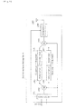
- FIG. 1 is a block diagram of a contactless IC card reader/writer.
- the contactless IC card reader/writer (hereinafter referred to simply as "a reader/writer") according to this embodiment performs processings related to electronic money, such as settlement processing and balance confirmation, for an IC card in which a contactless IC chip functioning as an electronic wallet is buried.
- the reader/writer As shown in Figure 1, the reader/writer according to this embodiment is provided with communication units 100 for performing data communication with an IC card 10, and a main unit 200 for performing processings related to electronic money with the use of the communication units 100.
- the main unit 200 performs processing related to electronic money in response to a request from an external apparatus such as a vending machine and a control unit of a POS terminal, for example.
- the present invention is characterized in that multiple communication units 100 are connected to one main unit 200 via a communication line 300 as shown in Figure 1.
- Each of the communication units 100 is provided with a communication controller 110 for performing communication with the main unit 200, a reader/writer controller 120 for controlling data communication with an IC card 10, a high-frequency (RF) circuit 130 for communication with an IC card 10 and an antenna 140.
- the reader/writer controller 120 is provided with an encryption processor 121 for encrypting data communicated between the communication unit 100 and an IC card 10. Since electronic money information communicated wirelessly is encrypted by this, security is enhanced.
- the main unit 200 is provided with a communication controller 210 for performing communication with the communication units 100 and a main controller 220 for performing various processings related to electronic money using the communication unit 100 in response to an instruction from an external apparatus.
- a modem 230 is connected to the main controller 220 to enable communication with an electronic money management server 21 via a network 20.
- Data to be sent to the electronic money management server 21 by the main controller 220 is mainly settlement information about settlement performed with electronic money. This settlement information is encrypted by an encryption processor 221 provided for the main controller 220.
- Figure 2 is a diagram illustrating the form of connection between the communication units and the main unit.
- the communication units 100 and the main unit 200 are connected via buses.
- Each of the communication controller 110 of the communication unit 100 and the communication controller 210 of the main unit 200 is configured by a transceiver for bus connection.
- a transceiver for bus connection.
- various systems can be used, such as a polling system and a CSMA/CD system, for example.
- Figure 3 is a flowchart illustrating the operation of the main unit of the reader/writer.
- the main unit 200 When the power supply is on, the main unit 200 starts the operation and assigns an address (ID) to each of the connected multiple communication units 100 (step S1). Next, the main unit 200 performs authentication processing for confirming whether or not each of the communication units 100 is authorized (step S2). The above steps are the initial operation.
- the main unit 200 starts a polling operation to detect whether or not an IC card 10 has been detected in each of the communication units 100 (step S3).
- the main unit 200 instructs the communication unit 100 to perform authentication processing for the IC card 10 (step 55).
- the main unit 200 instructs the communication unit 100 to perform predetermined reading processing or writing processing specified by an external apparatus for the IC card 10 (step 56).
- the main unit 200 again returns to the polling operation.
- multiple communication units 100 can be connected to one main unit 200 in the reader/writer according to this embodiment, it is possible to construct a system capable of responding to multiple IC cards 10 inexpensively.
- the main unit 200 may permit or inhibit communication with the other communication units 100.
- master-slave communication in which the main unit 200 performs a polling operation to the communication units 100 has been shown as an example.
- an event type may be also possible in which, when the communication unit 100 detects an event such as detection of an IC card 10, the communication unit 100 accesses the main unit 200.
- Figure 4 is a block diagram of a contactless IC card reader/writer.
- the reader/writer according to this embodiment is different from that of the first embodiment in that the communication route between the main unit 200 and the communication unit 100 is wirelessly constructed.
- wireless relay units 240 and 150 are connected to the main unit 200 and each of the communication units 100 in this embodiment, as shown in Figure 4.
- Other configurations and operations are similar to those in the first embodiment.
- FIG. 5 is a block diagram of the wireless relay unit. Since the wireless relay unit 240 connected to the main unit 200 and the wireless relay units 150 connected to the communication units 100 are the same, only the wireless relay unit 240 connected to the main unit 200 will be described here, and description of the wireless relay units 150 connected to the communication units 100 will be omitted.
- the wireless relay unit 240 is provided with a controller 241 connected to the main unit 200, switches 242 and 243 for switching between a receiving-side circuit and a sending-side circuit, a modulator 244 and a transmitter 245 for converting a digital signal to an analog signal, a demodulator 246 and a receiver 247 for converting an analog signal to a digital signal, a frequency converter 248 for converting the frequency of an analog signal used by the transmitter 245 and the receiver 247 and the frequency of a wireless signal to be a carrier to each other, and an antenna 249.
- RS422 is used as a connection interface between the control unit 241 and the main unit 200.
- various protocols such as for the wireless frequency band and the modulation/demodulation systems, those that are well known are applicable.
- the present invention is not limited thereto.
- the contactless IC chip can be mounted on various equipment and objects, for example, a mobile phone, a watch, a PDA, a personal computer, a bracelet, a finger ring, an earring and the like.
- a contactless IC chip functioning as an electronic wallet has been described.
- the present invention can be applied to a contactless IC chip having another function.
- contactless IC chips functioning as a commuter pass, an employee ID card and a member card can be given. These multiple functions may be mounted.
- the modem 230 is separately provided so that the main unit 200 communicates with the electronic money management server 21.
- network communication equipment for example, a POS terminal is already provided as an external apparatus, this network communication equipment can be shared by the POS terminal and the main unit 200.
Landscapes
- Engineering & Computer Science (AREA)
- Artificial Intelligence (AREA)
- Computer Vision & Pattern Recognition (AREA)
- Physics & Mathematics (AREA)
- General Physics & Mathematics (AREA)
- Theoretical Computer Science (AREA)
- Control Of Vending Devices And Auxiliary Devices For Vending Devices (AREA)
- Credit Cards Or The Like (AREA)
Abstract
In a contactless IC chip reader/writer comprising communication units 100 for performing data communication with a contactless IC chip and a main control unit 200 for controlling communication with a contactless IC chip 10 via the communication unit 100 in response to a request from an external apparatus, plural communication units are provided for one main control unit; and the main control unit and each communication unit are provided with a communication controller for performing data communication between each communication unit and the main control unit.
Description
- The present invention relates to a contactless IC chip reader/writer for writing and reading data to and from a contactless IC chip capable of functioning as a commuter pass, an employee ID card, a member card, an electronic wallet and the like.
- Recently, a contactless IC chip embedded a program which functions as a commuter pass, an employee ID card, a member card, an electronic purse and the like has been in widespread use. This contactless IC chip is actually used being buried in a card or a mobile phone. This contactless IC chip is caused to operate by an electric wave provided from a contactless IC chip reader/writer (hereinafter simply referred to as "a reader/writer").
- As a conventional reader/writer, the reader/writer described in
Patent Document 1 is known. The reader/writer described inPatent Document 1 is a reader/writer included in a vending machine, and its operation is controlled by a main computer. After performing electronic money settlement processing with the contactless IC chip using the reader/writer, the main computer sends settlement data to a predetermined server which manages electronic money.
Patent Document 1:Japanese Patent Publication No. 2001-229347 - When sending the settlement data to the predetermined server, the main computer is required to perform predetermined encryption processing decided with an electronic money management company for this settlement data. Since it is necessary to perform this encryption processing at a high speed, a high-performance arithmetic unit is required. Therefore, in the case of installing multiple readers/writers, there is a problem that a high-performance arithmetic unit is required for the conventional apparatus configuration, and the cost is increased.
- The present invention has been made in consideration of the above situation, and its object is to provide a contactless IC chip reader/writer capable of responding to multiple contactless IC chips at a low cost.
- In order to achieve the above object, this application proposes a contactless IC chip reader/writer comprising a communication unit for performing data communication with a contactless IC chip and a main control unit for controlling communication with a contactless IC chip via the communication unit in response to a request from an external apparatus, characterized in that: plural communication units are provided for one main control unit; and the main control unit and each communication unit are provided with a communication controller for performing data communication between each communication unit and the main control unit.
- According to the present invention, there are provided multiple communication units for communicating with a contactless IC chip for one main control unit to enable communication between the main control unit and each of the communication units. Consequently, it is possible to respond to multiple contactless IC chips at a low cost without increasing the number of main control units required to have a high arithmetic capability.
- The data communication route between the main control unit and each control unit may be wirelessly constructed. It may be wiredly constructed. It is preferable that the main control unit performs authentication processing for confirming whether or not each communication unit is authorized at least when a power supply is on, because it can prevent connection by unauthorized equipment.
- As described above, according to the present invention, there are provided multiple communication units for communicating with a contactless IC chip for one main control unit to enable communication between the main control unit and each of the communication units. Consequently, it is possible to respond to multiple contactless IC chips at a low cost without increasing the number of main control units required to have a high arithmetic capability.
-
- Figure 1 is a block diagram of a contactless IC chip reader/writer according to a first embodiment;
- Figure 2 is a diagram illustrating the form of connection between a main unit and communication units;
- Figure 3 is a flowchart illustrating the operation of the main unit;
- Figure 4 is a block diagram of a contactless IC chip reader/writer according to a second embodiment; and
- Figure 5 is a block diagram of a wireless relay unit.
-
- 10 ... contactless IC card
- 20 ... network
- 21 ... electronic money management server
- 100 ... communication unit
- 110 ... communication controller
- 120 ... reader/writer controller
- 121 ... encryption processor
- 130 ... high-frequency (RF) circuit
- 140 ... antenna
- 150 ... wireless relay unit
- 200 ... main unit
- 210 ... communication controller
- 220 ... main controller
- 221 ... encryption processor
- 230 ... modem
- 240 ... wireless relay unit
- 300 ... communication cable
- A contactless IC card reader/writer according to an embodiment of the present invention will be described with reference to drawings. Figure 1 is a block diagram of a contactless IC card reader/writer. The contactless IC card reader/writer (hereinafter referred to simply as "a reader/writer") according to this embodiment performs processings related to electronic money, such as settlement processing and balance confirmation, for an IC card in which a contactless IC chip functioning as an electronic wallet is buried.
- As shown in Figure 1, the reader/writer according to this embodiment is provided with
communication units 100 for performing data communication with anIC card 10, and amain unit 200 for performing processings related to electronic money with the use of thecommunication units 100. Themain unit 200 performs processing related to electronic money in response to a request from an external apparatus such as a vending machine and a control unit of a POS terminal, for example. The present invention is characterized in thatmultiple communication units 100 are connected to onemain unit 200 via acommunication line 300 as shown in Figure 1. - Each of the
communication units 100 is provided with acommunication controller 110 for performing communication with themain unit 200, a reader/writer controller 120 for controlling data communication with anIC card 10, a high-frequency (RF)circuit 130 for communication with anIC card 10 and anantenna 140. The reader/writer controller 120 is provided with anencryption processor 121 for encrypting data communicated between thecommunication unit 100 and anIC card 10. Since electronic money information communicated wirelessly is encrypted by this, security is enhanced. - The
main unit 200 is provided with acommunication controller 210 for performing communication with thecommunication units 100 and amain controller 220 for performing various processings related to electronic money using thecommunication unit 100 in response to an instruction from an external apparatus. Amodem 230 is connected to themain controller 220 to enable communication with an electronicmoney management server 21 via anetwork 20. Data to be sent to the electronicmoney management server 21 by themain controller 220 is mainly settlement information about settlement performed with electronic money. This settlement information is encrypted by anencryption processor 221 provided for themain controller 220. - Next, the form of connection between each of the
communication units 100 and themain unit 200 will be described with reference to Figure 2. Figure 2 is a diagram illustrating the form of connection between the communication units and the main unit. - As shown in Figure 2, the
communication units 100 and themain unit 200 are connected via buses. Each of thecommunication controller 110 of thecommunication unit 100 and thecommunication controller 210 of themain unit 200 is configured by a transceiver for bus connection. As the bus access control system used in such a connection form, various systems can be used, such as a polling system and a CSMA/CD system, for example. - Next, the operation of this reader/writer will be described with reference to the flowchart in Figure 3. Figure 3 is a flowchart illustrating the operation of the main unit of the reader/writer.
- When the power supply is on, the
main unit 200 starts the operation and assigns an address (ID) to each of the connected multiple communication units 100 (step S1). Next, themain unit 200 performs authentication processing for confirming whether or not each of thecommunication units 100 is authorized (step S2). The above steps are the initial operation. - Subsequently, the
main unit 200 starts a polling operation to detect whether or not anIC card 10 has been detected in each of the communication units 100 (step S3). When detecting that any of thecommunication units 100 has detected an IC card 10 (step S4), themain unit 200 instructs thecommunication unit 100 to perform authentication processing for the IC card 10 (step 55). When receiving that the authentication processing has been completed from thecommunication unit 100, themain unit 200 instructs thecommunication unit 100 to perform predetermined reading processing or writing processing specified by an external apparatus for the IC card 10 (step 56). When the reading/writing processing is completed, themain unit 200 again returns to the polling operation. - As described above, since
multiple communication units 100 can be connected to onemain unit 200 in the reader/writer according to this embodiment, it is possible to construct a system capable of responding tomultiple IC cards 10 inexpensively. - While writing/reading of data to/from an
IC card 10 is being performed with the use of acertain communication unit 100, themain unit 200 may permit or inhibit communication with theother communication units 100. - In the above embodiment, master-slave communication in which the
main unit 200 performs a polling operation to thecommunication units 100 has been shown as an example. However, an event type may be also possible in which, when thecommunication unit 100 detects an event such as detection of anIC card 10, thecommunication unit 100 accesses themain unit 200. - A reader/writer according to a second embodiment of the present invention will be described with reference to drawings. Figure 4 is a block diagram of a contactless IC card reader/writer.
- The reader/writer according to this embodiment is different from that of the first embodiment in that the communication route between the
main unit 200 and thecommunication unit 100 is wirelessly constructed. In order to realize the wireless communication route,wireless relay units main unit 200 and each of thecommunication units 100 in this embodiment, as shown in Figure 4. Other configurations and operations are similar to those in the first embodiment. - The configuration of the wireless relay unit will be described with reference to Figure 5. Figure 5 is a block diagram of the wireless relay unit. Since the
wireless relay unit 240 connected to themain unit 200 and thewireless relay units 150 connected to thecommunication units 100 are the same, only thewireless relay unit 240 connected to themain unit 200 will be described here, and description of thewireless relay units 150 connected to thecommunication units 100 will be omitted. - The
wireless relay unit 240 is provided with acontroller 241 connected to themain unit 200,switches modulator 244 and atransmitter 245 for converting a digital signal to an analog signal, ademodulator 246 and areceiver 247 for converting an analog signal to a digital signal, afrequency converter 248 for converting the frequency of an analog signal used by thetransmitter 245 and thereceiver 247 and the frequency of a wireless signal to be a carrier to each other, and anantenna 249. RS422 is used as a connection interface between thecontrol unit 241 and themain unit 200. As for various protocols, such as for the wireless frequency band and the modulation/demodulation systems, those that are well known are applicable. - According to this embodiment, since the communicat ion route between the
main unit 200 and each of thecommunication units 100 is wirelessly constructed, various layout of each equipment can be designed. Other operations and advantages are the same as those of the first embodiment. - The embodiments of the present invention have been described. However, the present invention is not limited thereto. For example, though an
IC card 10 in which a contactless IC chip is buried has been described in the above embodiments, the contactless IC chip can be mounted on various equipment and objects, for example, a mobile phone, a watch, a PDA, a personal computer, a bracelet, a finger ring, an earring and the like. - In the above embodiments, a contactless IC chip functioning as an electronic wallet has been described. However, the present invention can be applied to a contactless IC chip having another function. For example, contactless IC chips functioning as a commuter pass, an employee ID card and a member card can be given. These multiple functions may be mounted.
- Furthermore, in the above embodiments, the
modem 230 is separately provided so that themain unit 200 communicates with the electronicmoney management server 21. However, if network communication equipment, for example, a POS terminal is already provided as an external apparatus, this network communication equipment can be shared by the POS terminal and themain unit 200. - Furthermore, the form of connection between the
main unit 200 and thecommunication units 100 illustrated in the above embodiments is only an example, and various communication systems and protocols can be used.
Claims (5)
- A contactless IC chip reader/writer comprising a communication unit for performing data communication with a contactless IC chip and a main control unit for controlling communication with a contactless IC chip via the communication unit in response to a request from an external apparatus, characterized in that:plural communication units are provided for one main control unit; andthe main control unit and each communication unit are provided with a communication controller for performing data communication between each communication unit and the main control unit.
- The contactless IC chip reader/writer according to claim 1, characterized in that the communication controller of the main control unit and each communication unit control wired data communication.
- The contactless IC chip reader/writer according to claim 1, characterized in that the communication controller of the main control unit and each communication unit control wireless data communication.
- The contactless IC chip reader/writer according to any one of claims 1 to 3, characterized in that the main control unit performs authentication processing for confirming whether or not each communication unit is authorized at least when a power supply is on.
- The contactless IC chip reader/writer according to any one of claims 1 to 4, characterized in that the main control unit performs settlement processing with electronic money for a contactless IC chip which functions as an electronic wallet.
Applications Claiming Priority (2)
| Application Number | Priority Date | Filing Date | Title |
|---|---|---|---|
| JP2004228245A JP2006048360A (en) | 2004-08-04 | 2004-08-04 | Non-contact ic chip reader/writer |
| PCT/JP2005/013816 WO2006013770A1 (en) | 2004-08-04 | 2005-07-28 | Reader/writer for non-contact ic chip |
Publications (1)
| Publication Number | Publication Date |
|---|---|
| EP1785915A1 true EP1785915A1 (en) | 2007-05-16 |
Family
ID=35787058
Family Applications (1)
| Application Number | Title | Priority Date | Filing Date |
|---|---|---|---|
| EP05767228A Withdrawn EP1785915A1 (en) | 2004-08-04 | 2005-07-28 | Reader/writer for non-contact ic chip |
Country Status (4)
| Country | Link |
|---|---|
| US (1) | US20080048036A1 (en) |
| EP (1) | EP1785915A1 (en) |
| JP (1) | JP2006048360A (en) |
| WO (1) | WO2006013770A1 (en) |
Cited By (2)
| Publication number | Priority date | Publication date | Assignee | Title |
|---|---|---|---|---|
| WO2010044041A1 (en) * | 2008-10-15 | 2010-04-22 | Logomotion, S.R.O. | The method of communication with the pos terminal, the frequency converter for the pos terminal |
| US10332087B2 (en) | 2009-05-03 | 2019-06-25 | Smk Corporation | POS payment terminal and a method of direct debit payment transaction using a mobile communication device, such as a mobile phone |
Families Citing this family (17)
| Publication number | Priority date | Publication date | Assignee | Title |
|---|---|---|---|---|
| JP2007314772A (en) * | 2006-04-28 | 2007-12-06 | Kansai Paint Co Ltd | Paint compounding information acquisition method of toning paint for obtaining desired color, and compounding information acquisition system |
| SK50042008A3 (en) * | 2008-01-04 | 2009-09-07 | Logomotion, S. R. O. | Method and system for authentication preferably at payments, identifier of identity and/or agreement |
| SK288721B6 (en) * | 2008-03-25 | 2020-01-07 | Smk Kk | Method, circuit and carrier for perform multiple operations on the keypad of mobile communication equipment |
| EP2329563A2 (en) * | 2008-08-29 | 2011-06-08 | Logomotion, s.r.o. | Removable card for a contactless communication, its utilization and the method of production |
| SK288757B6 (en) * | 2008-09-19 | 2020-05-04 | Smk Kk | System and method for contactless payment authorization |
| SK50862008A3 (en) * | 2008-09-19 | 2010-06-07 | Logomotion, S. R. O. | System for electronic payment applications and method for payment authorization |
| SK288747B6 (en) * | 2009-04-24 | 2020-04-02 | Smk Kk | Method and system for cashless payment transactions, particularly with contactless payment device using |
| US9098845B2 (en) * | 2008-09-19 | 2015-08-04 | Logomotion, S.R.O. | Process of selling in electronic shop accessible from the mobile communication device |
| SK500092009A3 (en) * | 2009-02-27 | 2010-09-07 | Logomotion, S. R. O. | Computer mouse for data transmission, preferably at electronic payment, method for data transmission |
| US11138573B2 (en) | 2011-10-25 | 2021-10-05 | Isi Corporation | Electronic money transfer payment method and system for same |
| US9313609B2 (en) | 2012-12-28 | 2016-04-12 | Joseph Nicholi Prencipe | Contact information social exchange method and system |
| US10281953B2 (en) | 2013-11-29 | 2019-05-07 | Motiv Inc. | Wearable device and data transmission method |
| EP4071581B1 (en) | 2013-11-29 | 2025-10-08 | Ouraring Inc. | Wearable computing device |
| JP6711511B2 (en) * | 2016-02-24 | 2020-06-17 | サンデン・リテールシステム株式会社 | Reader/writer for vending machine and vending machine including the same |
| EP3872733A1 (en) | 2020-02-26 | 2021-09-01 | Mastercard International Incorporated | Communication of sensitive data in restricted data channel |
| GB2598108A (en) * | 2020-08-17 | 2022-02-23 | Mastercard International Inc | Card reader, smart card and method for processing a transaction |
| US12288213B2 (en) | 2022-03-16 | 2025-04-29 | Mastercard International Incorporated | Systems, methods and computer program products for secure contactless payment transactions |
Family Cites Families (6)
| Publication number | Priority date | Publication date | Assignee | Title |
|---|---|---|---|---|
| EP1249800A3 (en) * | 1996-05-31 | 2004-02-04 | Hitachi, Ltd. | Electronic money storing apparatus and IC card control method |
| JP3629891B2 (en) * | 1996-05-31 | 2005-03-16 | 株式会社日立製作所 | Electronic money control apparatus and control method thereof |
| JPH11345294A (en) * | 1998-06-03 | 1999-12-14 | Hitachi Ltd | Reader and / or writer system and communication system using the same |
| JP2001036545A (en) * | 1999-05-17 | 2001-02-09 | Sony Corp | Information processing apparatus and method, information processing system, and medium |
| JP2001291153A (en) * | 2000-04-05 | 2001-10-19 | Toshiba Electric Appliance Co Ltd | Vending machine abnormality notification device |
| US7197298B2 (en) * | 2003-04-23 | 2007-03-27 | Alps Electric Co., Ltd. | Radio-communication terminal device that prevents communication through an unauthenticated antenna |
-
2004
- 2004-08-04 JP JP2004228245A patent/JP2006048360A/en active Pending
-
2005
- 2005-07-28 US US11/572,187 patent/US20080048036A1/en not_active Abandoned
- 2005-07-28 EP EP05767228A patent/EP1785915A1/en not_active Withdrawn
- 2005-07-28 WO PCT/JP2005/013816 patent/WO2006013770A1/en not_active Ceased
Non-Patent Citations (1)
| Title |
|---|
| See references of WO2006013770A1 * |
Cited By (2)
| Publication number | Priority date | Publication date | Assignee | Title |
|---|---|---|---|---|
| WO2010044041A1 (en) * | 2008-10-15 | 2010-04-22 | Logomotion, S.R.O. | The method of communication with the pos terminal, the frequency converter for the pos terminal |
| US10332087B2 (en) | 2009-05-03 | 2019-06-25 | Smk Corporation | POS payment terminal and a method of direct debit payment transaction using a mobile communication device, such as a mobile phone |
Also Published As
| Publication number | Publication date |
|---|---|
| US20080048036A1 (en) | 2008-02-28 |
| WO2006013770A1 (en) | 2006-02-09 |
| JP2006048360A (en) | 2006-02-16 |
Similar Documents
| Publication | Publication Date | Title |
|---|---|---|
| US20080048036A1 (en) | Contactless Ic Chip Reader/Writer | |
| EP2064649B1 (en) | Near field connection establishment | |
| US8177131B2 (en) | Data communication system, device for executing IC card function, control method for the device, and information processing terminal | |
| KR101002042B1 (en) | Devices, modules and methods for the operation of antennas shared in RF technology-based communication environment | |
| US20110053556A1 (en) | Computer Mouse For Secure Communication With A Mobile Communication Device | |
| US8718551B2 (en) | Method and apparatus for a multi-band, multi-mode smartcard | |
| US7624927B2 (en) | Contactless card and a control method thereof | |
| EP2874111B1 (en) | Wireless power supply to enable payment transaction | |
| JP4757542B2 (en) | Non-contact IC device and control method | |
| US9219519B2 (en) | Proximity wireless transmission/reception device | |
| EP3806528B1 (en) | CONTACTLESS COMMUNICATION METHOD AND COMMUNICATION DEVICE | |
| US9712656B2 (en) | Control device, communication apparatus, control system, control method and storage medium | |
| EP3531569B1 (en) | Transaction device capable of managing and routing power from an external power source | |
| KR20140016444A (en) | Digital system for card settlement by tagging, settlment side system and providing method thereof | |
| JP4799058B2 (en) | IC card and computer program | |
| JP2006243970A (en) | Ic card system | |
| CN121396271A (en) | Near field communication system and electronic equipment | |
| JP5518109B2 (en) | COMMUNICATION DEVICE, COMMUNICATION METHOD, AND PROGRAM | |
| CN101969495B (en) | Portable electronic device | |
| KR20140011997A (en) | Digital system for card settlement by tagging, settlment side system and providing method thereof | |
| HK1186862A (en) | Service terminal, nfc device and near-field communication method |
Legal Events
| Date | Code | Title | Description |
|---|---|---|---|
| PUAI | Public reference made under article 153(3) epc to a published international application that has entered the european phase |
Free format text: ORIGINAL CODE: 0009012 |
|
| 17P | Request for examination filed |
Effective date: 20070122 |
|
| AK | Designated contracting states |
Kind code of ref document: A1 Designated state(s): DE ES FR GB IT |
|
| DAX | Request for extension of the european patent (deleted) | ||
| RBV | Designated contracting states (corrected) |
Designated state(s): DE ES FR GB IT |
|
| STAA | Information on the status of an ep patent application or granted ep patent |
Free format text: STATUS: THE APPLICATION IS DEEMED TO BE WITHDRAWN |
|
| 18D | Application deemed to be withdrawn |
Effective date: 20100202 |