EP1780842A1 - Photoelectric composite type connector, and substrate using the connector - Google Patents
Photoelectric composite type connector, and substrate using the connector Download PDFInfo
- Publication number
- EP1780842A1 EP1780842A1 EP05766319A EP05766319A EP1780842A1 EP 1780842 A1 EP1780842 A1 EP 1780842A1 EP 05766319 A EP05766319 A EP 05766319A EP 05766319 A EP05766319 A EP 05766319A EP 1780842 A1 EP1780842 A1 EP 1780842A1
- Authority
- EP
- European Patent Office
- Prior art keywords
- connector
- unit
- electrical
- connector unit
- photoelectric conversion
- Prior art date
- Legal status (The legal status is an assumption and is not a legal conclusion. Google has not performed a legal analysis and makes no representation as to the accuracy of the status listed.)
- Withdrawn
Links
Images



Classifications
-
- H—ELECTRICITY
- H01—ELECTRIC ELEMENTS
- H01R—ELECTRICALLY-CONDUCTIVE CONNECTIONS; STRUCTURAL ASSOCIATIONS OF A PLURALITY OF MUTUALLY-INSULATED ELECTRICAL CONNECTING ELEMENTS; COUPLING DEVICES; CURRENT COLLECTORS
- H01R13/00—Details of coupling devices of the kinds covered by groups H01R12/70 or H01R24/00 - H01R33/00
- H01R13/66—Structural association with built-in electrical component
- H01R13/665—Structural association with built-in electrical component with built-in electronic circuit
-
- G—PHYSICS
- G02—OPTICS
- G02B—OPTICAL ELEMENTS, SYSTEMS OR APPARATUS
- G02B6/00—Light guides; Structural details of arrangements comprising light guides and other optical elements, e.g. couplings
- G02B6/24—Coupling light guides
- G02B6/42—Coupling light guides with opto-electronic elements
- G02B6/4201—Packages, e.g. shape, construction, internal or external details
-
- G—PHYSICS
- G02—OPTICS
- G02B—OPTICAL ELEMENTS, SYSTEMS OR APPARATUS
- G02B6/00—Light guides; Structural details of arrangements comprising light guides and other optical elements, e.g. couplings
- G02B6/24—Coupling light guides
- G02B6/42—Coupling light guides with opto-electronic elements
- G02B6/4201—Packages, e.g. shape, construction, internal or external details
- G02B6/4274—Electrical aspects
- G02B6/4284—Electrical aspects of optical modules with disconnectable electrical connectors
-
- G—PHYSICS
- G02—OPTICS
- G02B—OPTICAL ELEMENTS, SYSTEMS OR APPARATUS
- G02B6/00—Light guides; Structural details of arrangements comprising light guides and other optical elements, e.g. couplings
- G02B6/24—Coupling light guides
- G02B6/42—Coupling light guides with opto-electronic elements
- G02B6/4292—Coupling light guides with opto-electronic elements the light guide being disconnectable from the opto-electronic element, e.g. mutually self aligning arrangements
-
- H—ELECTRICITY
- H01—ELECTRIC ELEMENTS
- H01R—ELECTRICALLY-CONDUCTIVE CONNECTIONS; STRUCTURAL ASSOCIATIONS OF A PLURALITY OF MUTUALLY-INSULATED ELECTRICAL CONNECTING ELEMENTS; COUPLING DEVICES; CURRENT COLLECTORS
- H01R31/00—Coupling parts supported only by co-operation with counterpart
- H01R31/06—Intermediate parts for linking two coupling parts, e.g. adapter
-
- G—PHYSICS
- G02—OPTICS
- G02B—OPTICAL ELEMENTS, SYSTEMS OR APPARATUS
- G02B6/00—Light guides; Structural details of arrangements comprising light guides and other optical elements, e.g. couplings
- G02B6/24—Coupling light guides
- G02B6/42—Coupling light guides with opto-electronic elements
- G02B6/4201—Packages, e.g. shape, construction, internal or external details
- G02B6/4204—Packages, e.g. shape, construction, internal or external details the coupling comprising intermediate optical elements, e.g. lenses, holograms
- G02B6/4214—Packages, e.g. shape, construction, internal or external details the coupling comprising intermediate optical elements, e.g. lenses, holograms the intermediate optical element having redirecting reflective means, e.g. mirrors, prisms for deflecting the radiation from horizontal to down- or upward direction toward a device
-
- H—ELECTRICITY
- H01—ELECTRIC ELEMENTS
- H01R—ELECTRICALLY-CONDUCTIVE CONNECTIONS; STRUCTURAL ASSOCIATIONS OF A PLURALITY OF MUTUALLY-INSULATED ELECTRICAL CONNECTING ELEMENTS; COUPLING DEVICES; CURRENT COLLECTORS
- H01R24/00—Two-part coupling devices, or either of their cooperating parts, characterised by their overall structure
- H01R24/60—Contacts spaced along planar side wall transverse to longitudinal axis of engagement
-
- H—ELECTRICITY
- H01—ELECTRIC ELEMENTS
- H01R—ELECTRICALLY-CONDUCTIVE CONNECTIONS; STRUCTURAL ASSOCIATIONS OF A PLURALITY OF MUTUALLY-INSULATED ELECTRICAL CONNECTING ELEMENTS; COUPLING DEVICES; CURRENT COLLECTORS
- H01R33/00—Coupling devices specially adapted for supporting apparatus and having one part acting as a holder providing support and electrical connection via a counterpart which is structurally associated with the apparatus, e.g. lamp holders; Separate parts thereof
- H01R33/94—Holders formed as intermediate parts for linking a counter-part to a coupling part
Definitions
- the present invention relates to a photoelectric converter that is capable of conversion between light and electricity. Further, the present invention relates to a photoelectric composite connector and a substrate that can be used in such a photoelectric converter, i.e. a photoelectric composite connector using an electrical connector structure and a substrate using the photoelectric composite connector.
- a photoelectric converter has been widely used in such a manner that it is connected to optical transmission means such as an optical fiber so as to, for example, transmit a high-frequency electrical signal.
- the high-frequency electrical signal may have noise when the traveling distance is long.
- an optical signal is used in place of the electrical signal and a photoelectric converter is used at the end of transmission so as to convert the optical signal into the electrical signal or the electrical signal into the optical signal and use the electrical (or optical) signal.
- an attempt to use such an optical signal in short-distance connection e.g. on a substrate (between devices on the same substrate) or between substrates, by use of a small-sized photoelectric converter in particular has started.
- Illustrative examples of currently usable devices include a type having an optical waveguide embedded in a substrate and a type having a film waveguide laminated on a substrate.
- an optical signal is transmitted through a waveguide provided inside or outside a substrate, and the optical signal is converted into an electrical signal by a photoelectric conversion device which is provided separately from the above waveguide.
- another type has an optical member at the tip of an optical fiber as a plug-side connector and uses a photoelectric conversion device as the corresponding receptacle-side connector to perform conversion between light and electricity.
- these devices require a highly accurate optical alignment between the optical member or waveguide and the photoelectric conversion device and also require a highly accurate alignment between the optical member and the substrate when the optical member is soldered to the substrate.
- the substrate since the substrate hardly enjoys surface dimensional accuracy due to warpage or distortion, it is difficult to control such an alignment.
- these devices require a measure for dealing with degradation of the performance of light-emitting and light-receiving elements mounted in the devices, e.g. a measure for static electricity, it is difficult to take a measurement for the performance degradation since the light-emitting and light-receiving elements must be mounted on the substrate having a number of other electrical elements mounted thereon.
- the literature discloses a structure having an optical connector section, more specifically, a structure which enables an optical fiber to be connected to an optical connector section integrated with a waveguide having a photoelectric conversion device by means of an atonality core.
- the connector section used in this structure is a so-called optical connector section which is merely used for optical connection and is not used for electrical connection.
- a photoelectric converter having an integrated module i.e. a module comprising integration of waveguide (light path right-angle conversion waveguide) and a photoelectric conversion device, at the tip of an optical fiber
- a photoelectric converter having an integrated module i.e. a module comprising integration of waveguide (light path right-angle conversion waveguide) and a photoelectric conversion device, at the tip of an optical fiber
- ASET Advanced Electronic System Integration Study Debriefing Session taken place in the National Museum of Emerging Science and Innovation at June 13, 2003 under the auspices of Technology Research Association - Association of Super-Advanced Electronics Technologies (ASET) and others.
- the integrated module presented in the session is considered to be an effective constitution which facilitates an optical alignment between a' waveguide and a photoelectric conversion module.
- a problem of alignment between a device and a substrate still remains even in such a constitution.
- Patent Literature 1 Japanese Patent Laid-Open Publication No. 264587/2001
- Non-Patent Literature 1 Fourth Electronic System Integration Study Debriefing Session, (time) June 13, 2003, (place) National Museum of Emerging Science, (host) Technology Research Association - Association of Super-Advanced Electronics Technologies (ASET), (co-host) National Institute of Advanced Industrial Science and Technology (AIST), (sponsorship) New Energy and Industrial Technology Development Organization (NEDO)
- An object of the present invention is to provide a photoelectric composite connector that allows an accurate and easy optical alignment between a photoelectric conversion device and a waveguide and does not require as high accuracy in alignment between an optical member and a substrate as an optical connector does, and a substrate using the photoelectric composite connector.
- Another object of the present invention is to makes it possible to connect or disconnect a substrate by a connector and improve usability.
- an optical signal transmitted to a plug-side connector through optical transmission means is transmitted to a receptacle-side connector as an electrical signal, only after the optical signal is converted into the electrical signal by the plug-side connector.
- an electrical signal transmitted to the plug-side connector through the receptacle-side connector is transmitted as an optical signal through the optical transmission means connected to the plug-side connector, only after the electrical signal is converted into the optical signal by the plug-side connector. That is, not transmission of optical signal but only transmission of electrical signal is carried out between the plug-side connector and receptacle-side connector of the present invention. Therefore, according to the above constitution, a general electrical connector structure can be used between the plug-side connector and the receptacle-side connector.
- the present invention provides a photoelectric composite connector using the above principle.
- the photoelectric composite connector comprises:
- the above connector may be constituted such that the second connector unit comprises a photoelectric conversion module and an electrical connector section having the second conductor which is electrically connected to the photoelectric conversion module, and the first conductor of the electrical connector section of the first connector unit and the second conductor of the second connector unit are electrically connected to each other when the electrical connector section of the first connector unit and the electrical connector section of the second connector unit are connected to each other by use of their electrical connector structures.
- the photoelectric conversion module may comprise a photoelectric conversion device and a waveguide.
- the waveguide may be a waveguide which changes the direction of a light path at a right angle.
- both the waveguide and the photoelectric conversion device may be of matrix type.
- the photoelectric conversion device may be VCSEL, a photodiode or an organic thin film having a light emitting function.
- the second connector unit may be surface-mounted on a substrate. Further, the substrate may have a unit which drives the photoelectric conversion device. Further, the above connector may further comprise, between the first connector unit and the optical transmission means, an auxiliary connector which can be attached to and detached from the first connector unit freely and is connected to the optical transmission means. Further, in the above connector, the first connector unit I may be a plug-side connector and the second connector may be a receptacle-side connector.
- the present invention provides a substrate using a photoelectric composite connector, wherein the photoelectric composite connector comprises a first connector unit which is connected to optical transmission means, and a second connector unit which is mounted on the substrate and can be attached to and detached from the first connector unit freely, the first connector unit comprises a photoelectric conversion module and an electrical connector section having a first conductor which is electrically connected to the photoelectric conversion module, the second connector unit is formed as an electrical connector unit corresponding to the electrical connector section of the first connector unit and having a second conductor, and the first conductor of the electrical connector section of the first connector unit and the second conductor of the second connector unit are electrically connected to each other when the electrical connector section of the first connector unit and the second connector unit are connected to each other by use of their electrical connector structures.
- an electrical connector structure can be used for connection between substrates or connection on a substrate.
- a highly accurate alignment is not required between a photoelectric conversion device and a waveguide or between an optical member and a substrate.
- the present invention can make connection with a substrate easily by the electrical connector structure.
- Fig. 1 is a diagram showing an example of connection between substrates in particular, using a photoelectric composite connector according to a first embodiment of the present invention.
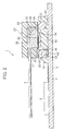
- Fig. 2 is a cross-sectional view at the center line of Fig. 1. It is needless to say that the photoelectric composite connector can be used for connection on a substrate and connection between devices as well as for connection between substrates.
- the photoelectric composite connector 1 comprises a plug-side connector 20 and a receptacle-side connector 40. These connectors 20 and 40 can be attached to and detached from each other freely. Fig. 1 shows the connectors in a detached state, and Fig. 2 shows them in an attached state. Further, although not clear from the drawings, the connector 1 may be considered to have a size of about 5 mm in length, about 5 mm in width and about 2 mm in thickness as a whole, for example.
- one end of optical transmission means such as an optical fiber 2 is connected to the plug-side connector 20, while the receptacle-side connector 40 is mounted on a surface of a substrate 3.
- the receptacle-side connector 40 When the receptacle-side connector 40 is surface-mounted on the substrate 3, it can be electrically connected to an IC driver for driving a device (photoelectric conversion device 24 to be described later) provided in the plug-side connector 20 via an electrical wire 5.
- an IC driver of this type has heretofore been integrally formed as a part of a photoelectric converter, the present invention provides the IC driver on the substrate 3 separately from the connector to reduce the size of the connector.
- the optical fiber 2 which is connected to the plug-side connector 20 may be a generally used optical fiber such as multicore- and array-type fibers as shown in the drawings.
- the receptacle-side connector 40 has an electrical connector structure to fit the plug-side connector 20 in the connector 40 at least on a side thereof on which the connector 20 fits the connector 40.
- the electrical connector structure is formed by the receptacle-side connector 40 itself. As is clear from using the electrical connector structure, only transmission of electrical signal is carried out between the plug-side connector 20 and the receptacle-side connector 40 in the present invention. Accordingly, it is satisfactory that the electrical connector structure and function of the receptacle-side connector 40 are at the same level as those of generally used electrical connectors.
- the receptacle-side connector 40 comprises, for example, a rectangular external wall 41, a rectangular island-shaped protruding section 42 which is situated inside the external wall 41, and a hollow section 43 which is formed between the external wall 41 and the protruding section 42.
- a plurality of conductors 44 which are partially exposed are provided in the direction in which the plug-side connector 20 fits in the connector 40 (although not clear from the drawings, eight conductors 44 are provided in total, at positions corresponding to conductors 23a to 23h to be described later of the plug-side connector 20).
- These conductors 44 penetrate through the inside of the receptacle-side connector 40 and extend toward the outside of the receptacle-side connector 40 and can be electrically connected to an electrical terminal 5 on the substrate.
- the receptacle-side connector 40 can be secured there in the same manner as generally used electrical connectors are secured, by soldering these extending portions 44' to the substrate 3.
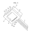
- Fig. 3 is a diagram showing the plug-side connector 20 and the optical fiber 2 connected thereto which are shown in Fig. 1 when viewed from a side thereof which fits the receptacle-side connector 40.
- Fig. 3 clearly shows the electrical connector structure of the plug-side connector 20 which corresponds to the electrical connector structure of the receptacle-side connector 40.
- the electrical connector structure of the plug-side connector 20 is not formed by the plug-side connector 20 itself but formed by an electrical connector section 21 which is provided as a part of it.
- the plug-side connector 20 has, for example, a protruding section 22 which has a rectangular hollow 33 in its central portion, to fit in the receptacle-side connector 40.
- a protruding section 22 which has a rectangular hollow 33 in its central portion, to fit in the receptacle-side connector 40.
- pairs of conductors 23a to 23h which correspond to the conductors 44 provided in the receptacle-side connector 40 along the direction in which the plug-side connector 20 fits in the receptacle-side connector 40.
- Fig. 4 is a diagram showing the plug-side connector 20 without the electrical connector section 21.
- Fig. 5 is a schematic perspective view of the electrical connector section 21 when viewed from a side thereof which contacts the plug-side connector.
- Fig. 6 is a schematic perspective view of the internal structure of the plug-side connector 20 in the state shown in Fig. 4.
- the plug-side connector 20 comprises a photoelectric conversion device 24, a waveguide 25, a housing 26 which surrounds these components 24 and 25, and the foregoing electrical connector section 21.
- the housing 26 is formed by an insulating material such as a synthetic resin and covers the whole waveguide 25 except for a side face 31 on which the plug-side connector 20 fits the receptacle-side connector 40.
- the photoelectric conversion device 24 and the waveguide 25 an integrated module of a photoelectric conversion device and a light path right-angle conversion waveguide described in Non-Patent Literature 1 is used, in particular.
- the light path right-angle conversion waveguide 25 which is provided adjacent to a pad 36 (refer to Fig. 2) has a mirror structure 32 which is disposed at an angle of about 45° to a light traveling direction and aligns tips by a fiber alignment plate 27, changes the direction of the light path of light 35 from each of the secured optical fibers 2 at a right angle and directs it to each spot 28 of the photoelectric conversion device 24 disposed in the light traveling direction.
- a light-receiving and light-emitting element such as VCSEL which is capable of emitting or receiving light from a number of spots at a time, a photodiode (PD) and an organic thin film having a light emitting function can be used.
- VCSEL photodiode
- PD photodiode
- organic thin film having a light emitting function By using not a mere waveguide but the light path right-angle conversion waveguide 25, the height (thickness) of the connector can be kept small, whereby a low-height mount, small-sized connector can be provided.
- a matrix-type light path right-angle conversion waveguide having a plurality of waveguides 25 aligned in parallel is particularly used as the light path right-angle conversion waveguide 25
- an alignment between multichannel cores and multichannel light-receiving and light-emitting elements is facilitated, and the size of the connector can be further reduced by reducing propagation loss.
- matrix-type VCSEL is used as the photoelectric conversion device 24, for example, an optical signal can be multichannel-transmitted, and a high-speed, large-capacity optical transmission system can be processed with parallel signals.
- the spots 28 of the photoelectric conversion device 24 are electrically connected to a plurality of electric wiring patterns 29 provided at the bottom of the integrated module.
- these electric wiring patterns 29a to 29h are connected to electric wiring patterns 30a to 30h provided in the electrical connector section 21, respectively.
- These electric wiring patterns 30a to 30h are connected to the conductors 23a to 23h in the plug-side connector 20, respectively.
- the electric wiring patterns 29a to 29h correspond to the conductors 23a to 23h, respectively. Therefore, according to the relationship between the electric wiring patterns 23a to 29h and the conductors 23a to 23h, the optical fibers 2 which correspond to the spots 28 of the photoelectric conversion device 24 correspond to the conductors 23a to 23h one-on-one.
- the connector can be so constituted as to deal with high-speed signals by adapting designs of these wires such as the lengths of the wires to high-frequency signals.
- the present invention is free of a problem of accuracy in alignment, unlike conventional devices which conduct the alignment with a substrate.
- the photoelectric conversion device 24 can be attached to the waveguide 25 by soldering. Upon soldering, the photoelectric conversion device 24 is subjected to very high heat. However, according to the constitution of the present invention, for example, when the waveguide 25 having the electric wiring patterns 29 and the electrical connector section 21 having the electric wiring patterns 30 are electrically conducted and secured by means (such as an electrically conductive adhesive and compression bonding) other than a heat process, the photoelectric conversion device 24 is subjected to such high heat only when it is soldered to the waveguide 25.
- means such as an electrically conductive adhesive and compression bonding
- the plug-side connector 20 and the receptacle-side connector 40 can be attached to and detached from each other freely by use of their electrical connector structures, there is no need to solder the waveguide 25 to the substrate 3 after the photoelectric conversion device 24 is soldered to the waveguide 25 as in the prior art, so that the photoelectric conversion device 24 is not subj ected to heat generated by the latter soldering operation.
- a load of heat on the photoelectric conversion device 24 or the waveguide 25 can be reduced, as compared with the prior art.
- Fig. 7 is a diagram showing an example of connection between substrates, using a photoelectric composite connector according to the second embodiment.
- Fig. 8 is a diagram showing a plug-side connector shown in Fig. 7 when viewed from a side thereof which fits a receptacle-side connector.
- Fig. 9 is a diagram showing the plug-side connector shown in Fig. 8 without an electrical connector section.
- Fig. 8 and Fig. 9 correspond to Fig. 3 and Fig. 4 in the first embodiment, respectively.
- the same numbers are allocated to the same members as those in the first embodiment with "A" added after the reference numbers.
- the second embodiment is different from the first embodiment primarily in that an auxiliary connector 60 is provided between an optical fiber 2 and a plug-side connector 20A.
- the auxiliary connector 60 can be attached to and detached from the plug-side connector 20A.
- the optical fiber 2 is connected not to the plug-side connector 20A but to the auxiliary connector 60.
- Such a constitution allows, for example, a number of different auxiliary connectors 60 to be connected to one plug-side connector 20A without connecting the optical fiber 2 to the plug-side connector 20A each time, thereby improving user-friendliness. Accordingly, an existing multicoreferrule (MT ferrule) can be used as the auxiliary connector.
- MT ferrule multicoreferrule
- the plug-side connector 20A can be connected to the auxiliary connector 60 by, for example, inserting two guide pins 34 which protrude from a side face of the plug-side connector 20A into corresponding holes 61 which are formed on a side face of the auxiliary connector 60 so as to guide the plug-side connector 20A to the auxiliary connector 60.
- they can be connected in alignment easily.
- they are optically linked at a number of portions 62. That is, in this case, a so-called multicore link is adopted.
- the present embodiment can also be applied to various other types of ferrules.
- their connection can be secured by, for example, using a clip which is elastically attached to these connectors along the entire extending direction of the connectors or placing and securing these connectors in a connector case to form a connector structure.
- the photoelectric composite connector of the present invention uses a general electrical connector structure. Therefore, although it can use light and electricity in combination, it is capable of connection between substrates, connection on a substrate or connection between devices in the same manner as general electrical connectors. Further, since this connector can use a generally used, standard electrical connector structure, a board designer can design circuits easily for the above connection between substrate or on a substrate, and transition of a printed circuit board for only electricity from a photoelectric composite printed circuit board can be achieved easily.
- the receptacle-side connector 40 itself is an electrical connector structure.
- the receptacle-side connector may be modified such that it has an electrical connector section as in the case of the plug-side connector 20.
- the plug-side connector 20 is provided at both ends of an optical fiber
- the receptacle-side connector 40 is provided on each of substrates to be connected to each other or at multiple spots on a substrate on which devices are connected to each other, and both ends of the plug-side connector 20 may be attached to and detached from the receptacle-side connector 40.
- the plug-side connector 20 is provided at one end of the optical fiber 2, a multicore connector similar to that described in Patent Literature 1 is provided at the other end, the one end is connected to the receptacle-side connector 40, and the other end is connected to a photoactive device.
- the plug-side connector 20 and the receptacle-side connector 40 can be directly connected to each other without a substrate, even in the connector structure of the present invention.
- the photoelectric composite connector according to the present invention can be easily used for connection between substrates or connection on a substrate.
Landscapes
- Physics & Mathematics (AREA)
- General Physics & Mathematics (AREA)
- Optics & Photonics (AREA)
- Engineering & Computer Science (AREA)
- Microelectronics & Electronic Packaging (AREA)
- Optical Couplings Of Light Guides (AREA)
- Details Of Connecting Devices For Male And Female Coupling (AREA)
Abstract
A photoelectric composite connector comprises a first connector unit which is connected to optical transmission means and a second connector unit which can be attached to and detached from a first connector unit freely. The first connector unit comprises a photoelectric conversion module and an electrical connector section having a first conductor which is electrically connected to the photoelectric conversion module. The second connector unit is formed as an electrical connector unit corresponding to the electrical connector section of the first connector unit and having a second conductor. The first conductor of the electrical connector section of the first connector unit and the second conductor of the second connector unit are electrically connected to each other when the electrical connector section of the first connector unit and the second connector unit are connected to each other by use of their electrical connector structures.
Description
- The present invention relates to a photoelectric converter that is capable of conversion between light and electricity. Further, the present invention relates to a photoelectric composite connector and a substrate that can be used in such a photoelectric converter, i.e. a photoelectric composite connector using an electrical connector structure and a substrate using the photoelectric composite connector.
- A photoelectric converter has been widely used in such a manner that it is connected to optical transmission means such as an optical fiber so as to, for example, transmit a high-frequency electrical signal. As is well known, the high-frequency electrical signal may have noise when the traveling distance is long. Thus, it is often practiced that an optical signal is used in place of the electrical signal and a photoelectric converter is used at the end of transmission so as to convert the optical signal into the electrical signal or the electrical signal into the optical signal and use the electrical (or optical) signal.
- In recent years, an attempt to use such an optical signal in short-distance connection, e.g. on a substrate (between devices on the same substrate) or between substrates, by use of a small-sized photoelectric converter in particular has started. Illustrative examples of currently usable devices include a type having an optical waveguide embedded in a substrate and a type having a film waveguide laminated on a substrate. In the case of these types, an optical signal is transmitted through a waveguide provided inside or outside a substrate, and the optical signal is converted into an electrical signal by a photoelectric conversion device which is provided separately from the above waveguide. In addition to these types, another type has an optical member at the tip of an optical fiber as a plug-side connector and uses a photoelectric conversion device as the corresponding receptacle-side connector to perform conversion between light and electricity. However, these devices require a highly accurate optical alignment between the optical member or waveguide and the photoelectric conversion device and also require a highly accurate alignment between the optical member and the substrate when the optical member is soldered to the substrate. In particular, since the substrate hardly enjoys surface dimensional accuracy due to warpage or distortion, it is difficult to control such an alignment. Further, although these devices require a measure for dealing with degradation of the performance of light-emitting and light-receiving elements mounted in the devices, e.g. a measure for static electricity, it is difficult to take a measurement for the performance degradation since the light-emitting and light-receiving elements must be mounted on the substrate having a number of other electrical elements mounted thereon.
- With respect to an optical alignment, a technique for facilitating an optical alignment between an optical fiber and a waveguide is disclosed in
Japanese Patent Laid-Open Publication No. 264587/2001 - Further, with respect to a photoelectric converter, a photoelectric converter having an integrated module, i.e. a module comprising integration of waveguide (light path right-angle conversion waveguide) and a photoelectric conversion device, at the tip of an optical fiber has been presented in the fourth Electronic System Integration Study Debriefing Session taken place in the National Museum of Emerging Science and Innovation at June 13, 2003 under the auspices of Technology Research Association - Association of Super-Advanced Electronics Technologies (ASET) and others. The integrated module presented in the session is considered to be an effective constitution which facilitates an optical alignment between a' waveguide and a photoelectric conversion module. However, a problem of alignment between a device and a substrate still remains even in such a constitution. Patent Literature 1:
Japanese Patent Laid-Open Publication No. 264587/2001
Non-Patent Literature 1: Fourth Electronic System Integration Study Debriefing Session, (time) June 13, 2003, (place) National Museum of Emerging Science, (host) Technology Research Association - Association of Super-Advanced Electronics Technologies (ASET), (co-host) National Institute of Advanced Industrial Science and Technology (AIST), (sponsorship) New Energy and Industrial Technology Development Organization (NEDO) - The present invention has been conceived to solve these problems of the prior art. An object of the present invention is to provide a photoelectric composite connector that allows an accurate and easy optical alignment between a photoelectric conversion device and a waveguide and does not require as high accuracy in alignment between an optical member and a substrate as an optical connector does, and a substrate using the photoelectric composite connector. Another object of the present invention is to makes it possible to connect or disconnect a substrate by a connector and improve usability.
- In a photoelectric composite connector according to the present invention, an optical signal transmitted to a plug-side connector through optical transmission means is transmitted to a receptacle-side connector as an electrical signal, only after the optical signal is converted into the electrical signal by the plug-side connector. Meanwhile, an electrical signal transmitted to the plug-side connector through the receptacle-side connector is transmitted as an optical signal through the optical transmission means connected to the plug-side connector, only after the electrical signal is converted into the optical signal by the plug-side connector. That is, not transmission of optical signal but only transmission of electrical signal is carried out between the plug-side connector and receptacle-side connector of the present invention. Therefore, according to the above constitution, a general electrical connector structure can be used between the plug-side connector and the receptacle-side connector.
- The present invention provides a photoelectric composite connector using the above principle. The photoelectric composite connector comprises:
- a first connector unit which is connected to optical transmission means, and
- a second connector unit which can be attached to and detached from the first connector unit freely,
- The above connector may be constituted such that the second connector unit comprises a photoelectric conversion module and an electrical connector section having the second conductor which is electrically connected to the photoelectric conversion module, and the first conductor of the electrical connector section of the first connector unit and the second conductor of the second connector unit are electrically connected to each other when the electrical connector section of the first connector unit and the electrical connector section of the second connector unit are connected to each other by use of their electrical connector structures.
- Further, in the above connector, the photoelectric conversion module may comprise a photoelectric conversion device and a waveguide. Further, the waveguide may be a waveguide which changes the direction of a light path at a right angle.
- Further, both the waveguide and the photoelectric conversion device may be of matrix type. Further, the photoelectric conversion device may be VCSEL, a photodiode or an organic thin film having a light emitting function.
- In the above connector, the second connector unit may be surface-mounted on a substrate. Further, the substrate may have a unit which drives the photoelectric conversion device. Further, the above connector may further comprise, between the first connector unit and the optical transmission means, an auxiliary connector which can be attached to and detached from the first connector unit freely and is connected to the optical transmission means. Further, in the above connector, the first connector unit I may be a plug-side connector and the second connector may be a receptacle-side connector.
- Further, the present invention provides a substrate using a photoelectric composite connector, wherein
the photoelectric composite connector comprises a first connector unit which is connected to optical transmission means, and a second connector unit which is mounted on the substrate and can be attached to and detached from the first connector unit freely,
the first connector unit comprises a photoelectric conversion module and an electrical connector section having a first conductor which is electrically connected to the photoelectric conversion module,
the second connector unit is formed as an electrical connector unit corresponding to the electrical connector section of the first connector unit and having a second conductor, and
the first conductor of the electrical connector section of the first connector unit and the second conductor of the second connector unit are electrically connected to each other when the electrical connector section of the first connector unit and the second connector unit are connected to each other by use of their electrical connector structures. - Despite use of an optical signal, an electrical connector structure can be used for connection between substrates or connection on a substrate. In the present invention, a highly accurate alignment is not required between a photoelectric conversion device and a waveguide or between an optical member and a substrate. Further, the present invention can make connection with a substrate easily by the electrical connector structure.
-
- Fig. 1 is a diagram showing an example of connection using a photoelectric composite connector according to a first embodiment of the present invention.
- Fig. 2 is a cross-sectional view at the center line of Fig. 1.
- Fig. 3 is a diagram showing a plug-side connector shown in Fig. 1 when viewed from a side thereof which fits a receptacle-side connector.
- Fig. 4 is a diagram showing the plug-side connector shown in Fig. 3 without an electrical connector section.
- Fig. 5 is a schematic perspective view of the electrical connector section when viewed from a side thereof which contacts the plug-side connector.
- Fig. 6 is a schematic perspective view of the internal structure of the plug-side connector in the state shown in Fig. 4.
- Fig. 7 is a diagram showing an example of connection using a photoelectric composite connector according to a second embodiment of the present invention.
- Fig. 8 is a diagram showing a plug-side connector shown in Fig. 7 when viewed from a side thereof which fits a receptacle-side connector.
- Fig. 9 is a diagram showing the plug-side connector shown in Fig. 8 without an electrical connector section.
- Fig. 1 is a diagram showing an example of connection between substrates in particular, using a photoelectric composite connector according to a first embodiment of the present invention. Fig. 2 is a cross-sectional view at the center line of Fig. 1. It is needless to say that the photoelectric composite connector can be used for connection on a substrate and connection between devices as well as for connection between substrates.
- The photoelectric
composite connector 1 comprises a plug-side connector 20 and a receptacle-side connector 40. Theseconnectors connector 1 may be considered to have a size of about 5 mm in length, about 5 mm in width and about 2 mm in thickness as a whole, for example. - In this application example, for example, one end of optical transmission means such as an
optical fiber 2 is connected to the plug-side connector 20, while the receptacle-side connector 40 is mounted on a surface of asubstrate 3. When the receptacle-side connector 40 is surface-mounted on thesubstrate 3, it can be electrically connected to an IC driver for driving a device (photoelectric conversion device 24 to be described later) provided in the plug-side connector 20 via anelectrical wire 5. While an IC driver of this type has heretofore been integrally formed as a part of a photoelectric converter, the present invention provides the IC driver on thesubstrate 3 separately from the connector to reduce the size of the connector. Theoptical fiber 2 which is connected to the plug-side connector 20 may be a generally used optical fiber such as multicore- and array-type fibers as shown in the drawings. - The receptacle-
side connector 40 has an electrical connector structure to fit the plug-side connector 20 in theconnector 40 at least on a side thereof on which theconnector 20 fits theconnector 40. The electrical connector structure is formed by the receptacle-side connector 40 itself. As is clear from using the electrical connector structure, only transmission of electrical signal is carried out between the plug-side connector 20 and the receptacle-side connector 40 in the present invention. Accordingly, it is satisfactory that the electrical connector structure and function of the receptacle-side connector 40 are at the same level as those of generally used electrical connectors. - As an example of the electrical connector structure described above, the receptacle-
side connector 40 comprises, for example, a rectangularexternal wall 41, a rectangular island-shaped protrudingsection 42 which is situated inside theexternal wall 41, and ahollow section 43 which is formed between theexternal wall 41 and the protrudingsection 42. On external surfaces that the protrudingsection 42 faces, a plurality ofconductors 44 which are partially exposed are provided in the direction in which the plug-side connector 20 fits in the connector 40 (although not clear from the drawings, eightconductors 44 are provided in total, at positions corresponding toconductors 23a to 23h to be described later of the plug-side connector 20). Theseconductors 44 penetrate through the inside of the receptacle-side connector 40 and extend toward the outside of the receptacle-side connector 40 and can be electrically connected to anelectrical terminal 5 on the substrate. The receptacle-side connector 40 can be secured there in the same manner as generally used electrical connectors are secured, by soldering these extending portions 44' to thesubstrate 3. - Fig. 3 is a diagram showing the plug-
side connector 20 and theoptical fiber 2 connected thereto which are shown in Fig. 1 when viewed from a side thereof which fits the receptacle-side connector 40. Fig. 3 clearly shows the electrical connector structure of the plug-side connector 20 which corresponds to the electrical connector structure of the receptacle-side connector 40. Unlike the electrical connector structure of the receptacle-side connector 40, the electrical connector structure of the plug-side connector 20 is not formed by the plug-side connector 20 itself but formed by anelectrical connector section 21 which is provided as a part of it. As described above, since only transmission of electrical signal is carried out between the plug-side connector 20 and the receptacle-side connector 40, it is satisfactory that the structure and function of theelectrical connector section 21 of the plug-side connector 20 are at the same level as those of generally used electrical connectors. - The plug-
side connector 20 has, for example, a protrudingsection 22 which has a rectangular hollow 33 in its central portion, to fit in the receptacle-side connector 40. On opposed internal surfaces of the protrudingsection 22, pairs ofconductors 23a to 23h which correspond to theconductors 44 provided in the receptacle-side connector 40 along the direction in which the plug-side connector 20 fits in the receptacle-side connector 40. When the protrudingsection 22 of the plug-side connector 20 fits in the hollow 43 of the receptacle-side connector 40, theseconductors side connector 20 and the receptacle-side connector 40. - Next, the structure of the plug-side connector will be further described with reference to Figs. 4 to 6 as well. Fig. 4 is a diagram showing the plug-
side connector 20 without theelectrical connector section 21. Fig. 5 is a schematic perspective view of theelectrical connector section 21 when viewed from a side thereof which contacts the plug-side connector. Fig. 6 is a schematic perspective view of the internal structure of the plug-side connector 20 in the state shown in Fig. 4. - The plug-
side connector 20 comprises aphotoelectric conversion device 24, awaveguide 25, ahousing 26 which surrounds thesecomponents electrical connector section 21. Thehousing 26 is formed by an insulating material such as a synthetic resin and covers thewhole waveguide 25 except for aside face 31 on which the plug-side connector 20 fits the receptacle-side connector 40. - As the
photoelectric conversion device 24 and thewaveguide 25, an integrated module of a photoelectric conversion device and a light path right-angle conversion waveguide described inNon-Patent Literature 1 is used, in particular. The light path right-angle conversion waveguide 25 which is provided adjacent to a pad 36 (refer to Fig. 2) has amirror structure 32 which is disposed at an angle of about 45° to a light traveling direction and aligns tips by afiber alignment plate 27, changes the direction of the light path of light 35 from each of the securedoptical fibers 2 at a right angle and directs it to eachspot 28 of thephotoelectric conversion device 24 disposed in the light traveling direction. As thephotoelectric conversion device 24, a light-receiving and light-emitting element such as VCSEL which is capable of emitting or receiving light from a number of spots at a time, a photodiode (PD) and an organic thin film having a light emitting function can be used. By using not a mere waveguide but the light path right-angle conversion waveguide 25, the height (thickness) of the connector can be kept small, whereby a low-height mount, small-sized connector can be provided. Further, when a matrix-type light path right-angle conversion waveguide having a plurality ofwaveguides 25 aligned in parallel is particularly used as the light path right-angle conversion waveguide 25, an alignment between multichannel cores and multichannel light-receiving and light-emitting elements is facilitated, and the size of the connector can be further reduced by reducing propagation loss. Further, when matrix-type VCSEL is used as thephotoelectric conversion device 24, for example, an optical signal can be multichannel-transmitted, and a high-speed, large-capacity optical transmission system can be processed with parallel signals. - The
spots 28 of thephotoelectric conversion device 24 are electrically connected to a plurality ofelectric wiring patterns 29 provided at the bottom of the integrated module. When the integrated module is constituted, theseelectric wiring patterns 29a to 29h are connected toelectric wiring patterns 30a to 30h provided in theelectrical connector section 21, respectively. Theseelectric wiring patterns 30a to 30h are connected to theconductors 23a to 23h in the plug-side connector 20, respectively. As a result, theelectric wiring patterns 29a to 29h correspond to theconductors 23a to 23h, respectively. Therefore, according to the relationship between theelectric wiring patterns 23a to 29h and theconductors 23a to 23h, theoptical fibers 2 which correspond to thespots 28 of thephotoelectric conversion device 24 correspond to theconductors 23a to 23h one-on-one. When the electrical signal is of high frequency, the connector can be so constituted as to deal with high-speed signals by adapting designs of these wires such as the lengths of the wires to high-frequency signals. Thus, since an optical alignment is conducted in the connector (plug-side connector 20) in the present invention, the present invention is free of a problem of accuracy in alignment, unlike conventional devices which conduct the alignment with a substrate. - The
photoelectric conversion device 24 can be attached to thewaveguide 25 by soldering. Upon soldering, thephotoelectric conversion device 24 is subjected to very high heat. However, according to the constitution of the present invention, for example, when thewaveguide 25 having theelectric wiring patterns 29 and theelectrical connector section 21 having theelectric wiring patterns 30 are electrically conducted and secured by means (such as an electrically conductive adhesive and compression bonding) other than a heat process, thephotoelectric conversion device 24 is subjected to such high heat only when it is soldered to thewaveguide 25. The reason is that in the photoelectric composite connector of the present invention, since the plug-side connector 20 and the receptacle-side connector 40 can be attached to and detached from each other freely by use of their electrical connector structures, there is no need to solder thewaveguide 25 to thesubstrate 3 after thephotoelectric conversion device 24 is soldered to thewaveguide 25 as in the prior art, so that thephotoelectric conversion device 24 is not subj ected to heat generated by the latter soldering operation. As a result, according to the constitution of the present invention, a load of heat on thephotoelectric conversion device 24 or thewaveguide 25 can be reduced, as compared with the prior art. - Next, a second embodiment of the present invention will be described with reference to Figs. 7 to 9. Fig. 7 is a diagram showing an example of connection between substrates, using a photoelectric composite connector according to the second embodiment. Fig. 8 is a diagram showing a plug-side connector shown in Fig. 7 when viewed from a side thereof which fits a receptacle-side connector. Fig. 9 is a diagram showing the plug-side connector shown in Fig. 8 without an electrical connector section. Fig. 8 and Fig. 9 correspond to Fig. 3 and Fig. 4 in the first embodiment, respectively. The same numbers are allocated to the same members as those in the first embodiment with "A" added after the reference numbers.
- The second embodiment is different from the first embodiment primarily in that an
auxiliary connector 60 is provided between anoptical fiber 2 and a plug-side connector 20A. Theauxiliary connector 60 can be attached to and detached from the plug-side connector 20A. In the present embodiment, theoptical fiber 2 is connected not to the plug-side connector 20A but to theauxiliary connector 60. Such a constitution allows, for example, a number of differentauxiliary connectors 60 to be connected to one plug-side connector 20A without connecting theoptical fiber 2 to the plug-side connector 20A each time, thereby improving user-friendliness. Accordingly, an existing multicoreferrule (MT ferrule) can be used as the auxiliary connector. - The plug-
side connector 20A can be connected to theauxiliary connector 60 by, for example, inserting two guide pins 34 which protrude from a side face of the plug-side connector 20A into correspondingholes 61 which are formed on a side face of theauxiliary connector 60 so as to guide the plug-side connector 20A to theauxiliary connector 60. By such a method, they can be connected in alignment easily. When they are connected in alignment, they are optically linked at a number ofportions 62. That is, in this case, a so-called multicore link is adopted. However, as a matter of course, the present embodiment can also be applied to various other types of ferrules. Although not particularly shown in the drawing, their connection can be secured by, for example, using a clip which is elastically attached to these connectors along the entire extending direction of the connectors or placing and securing these connectors in a connector case to form a connector structure. - As is clear from the above description, the photoelectric composite connector of the present invention uses a general electrical connector structure. Therefore, although it can use light and electricity in combination, it is capable of connection between substrates, connection on a substrate or connection between devices in the same manner as general electrical connectors. Further, since this connector can use a generally used, standard electrical connector structure, a board designer can design circuits easily for the above connection between substrate or on a substrate, and transition of a printed circuit board for only electricity from a photoelectric composite printed circuit board can be achieved easily.
- In the above example, the receptacle-
side connector 40 itself is an electrical connector structure. However, the receptacle-side connector may be modified such that it has an electrical connector section as in the case of the plug-side connector 20. Further, as a variation, for example, the plug-side connector 20 is provided at both ends of an optical fiber, the receptacle-side connector 40 is provided on each of substrates to be connected to each other or at multiple spots on a substrate on which devices are connected to each other, and both ends of the plug-side connector 20 may be attached to and detached from the receptacle-side connector 40. Further, it is also possible that the plug-side connector 20 is provided at one end of theoptical fiber 2, a multicore connector similar to that described inPatent Literature 1 is provided at the other end, the one end is connected to the receptacle-side connector 40, and the other end is connected to a photoactive device. - When an
IC driver 6 which drives thephotoelectric conversion device 24 is provided in the plug-side connector 20 or the receptacle-side connector 40 as in the prior art, the plug-side connector 20 and the receptacle-side connector 40 can be directly connected to each other without a substrate, even in the connector structure of the present invention. - Using an electrical connector structure, the photoelectric composite connector according to the present invention can be easily used for connection between substrates or connection on a substrate.
the first connector unit comprises a photoelectric conversion module and an electrical connector section having a first conductor which is electrically connected to the photoelectric conversion module,
the second connector unit is formed as an electrical connector unit corresponding to the electrical connector section of the first connector unit and having a second conductor, and
the first conductor of the electrical connector section of the first connector unit and the second conductor of the second connector unit are electrically connected to each other when the electrical connector section of the first connector unit and the second connector unit are connected to each other by use of their electrical connector structures.
Claims (11)
- A photoelectric composite connector comprising:a first connector unit which is connected to optical transmission means, anda second connector unit which can be attached to and detached from the first connector unit freely,whereinthe first connector unit comprises a photoelectric conversion module and an electrical connector section having a first conductor which is electrically connected to the photoelectric conversion module,the second connector unit is formed as an electrical connector unit corresponding to the electrical connector section of the first connector unit and having a second conductor, andthe first conductor of the electrical connector section of the first connector unit and the second conductor of the second connector unit are electrically connected to each other when the electrical connector section of the first connector unit and the second connector unit are connected to each other by use of their electrical connector structures.
- The connector of claim 1, wherein the second connector unit comprises a photoelectric conversion module and an electrical connector section having the second conductor which is electrically connected to the photoelectric conversion module, and the first conductor of the electrical connector section of the first connector unit and the second conductor of the second connector unit are electrically connected to each other when the electrical connector section of the first connector unit and the electrical connector section of the second connector unit are connected to each other by use of their electrical connector structures.
- The connector of claim 1 or 2, wherein the photoelectric conversion module comprises a photoelectric conversion device and a waveguide.
- The connector of claim 3, wherein the waveguide is a waveguide which changes the direction of a light path at a right angle.
- The connector of claim 3 or 4, wherein both the waveguide and the photoelectric conversion device are of matrix type.
- The connector of any of claims 3 to 5, wherein the photoelectric conversion device is VCSEL, a photodiode or an organic thin film having a light emitting function.
- The connector of claim 1 or any of claims 3 to 6, wherein the second connector unit is surface-mounted on a substrate.
- The connector of claim 7, wherein the substrate has a unit which drives the photoelectric conversion device.
- The connector of any of claims 1 to 8, further comprising, between the first connector unit and the optical transmission means, an auxiliary connector which can be attached to and detached from the first connector unit freely and is connected to the optical transmission means.
- The connector of claim 1, wherein the first connector unit is a plug-side connector, and the second connector is a receptacle-side connector.
- A substrate using a photoelectric composite connector,
wherein
the photoelectric composite connector comprises a first connector unit which is connected to optical transmission means, and a second connector unit which is mounted on the substrate and can be attached to and detached from the first connector unit freely,
the first connector unit comprises a photoelectric conversion module and an electrical connector section having a first conductor which is electrically connected to the photoelectric conversion module,
the second connector unit is formed as an electrical connector unit corresponding to the electrical connector section of the first connector unit and having a second conductor, and
the first conductor of the electrical connector section of the first connector unit and the second conductor of the second connector unit are electrically connected to each other when the electrical connector section of the first connector unit and the second connector unit are connected to each other by use of their electrical connector structures.
Applications Claiming Priority (2)
| Application Number | Priority Date | Filing Date | Title |
|---|---|---|---|
| JP2004213082A JP4238187B2 (en) | 2004-07-21 | 2004-07-21 | Photoelectric composite connector and board using the same |
| PCT/JP2005/013273 WO2006009156A1 (en) | 2004-07-21 | 2005-07-20 | Photoelectric composite type connector, and substrate using the connector |
Publications (2)
| Publication Number | Publication Date |
|---|---|
| EP1780842A1 true EP1780842A1 (en) | 2007-05-02 |
| EP1780842A4 EP1780842A4 (en) | 2007-09-19 |
Family
ID=35785264
Family Applications (1)
| Application Number | Title | Priority Date | Filing Date |
|---|---|---|---|
| EP05766319A Withdrawn EP1780842A4 (en) | 2004-07-21 | 2005-07-20 | COMPOSITE TYPE PHOTOELECTRIC CONNECTOR AND SUBSTRATE USING THE CONNECTOR |
Country Status (5)
| Country | Link |
|---|---|
| US (1) | US7488119B2 (en) |
| EP (1) | EP1780842A4 (en) |
| JP (1) | JP4238187B2 (en) |
| CN (1) | CN100566045C (en) |
| WO (1) | WO2006009156A1 (en) |
Cited By (3)
| Publication number | Priority date | Publication date | Assignee | Title |
|---|---|---|---|---|
| EP2093840A1 (en) * | 2008-02-20 | 2009-08-26 | Mitsumi Electric Co., Ltd. | Connector, optical transmission module and optical-electrical transmission module |
| WO2011119107A1 (en) * | 2010-03-24 | 2011-09-29 | Nitto Denko Corporation | An optical system |
| EP1726978B1 (en) * | 2005-05-24 | 2017-08-23 | Hirose Electric Co., Ltd. | Photoelectric combined connector |
Families Citing this family (25)
| Publication number | Priority date | Publication date | Assignee | Title |
|---|---|---|---|---|
| KR100825732B1 (en) | 2006-09-29 | 2008-04-29 | 한국전자통신연구원 | Photoelectric connector module and photoelectric communication module including the module |
| JP5113365B2 (en) * | 2006-09-29 | 2013-01-09 | パナソニック株式会社 | Photoelectric conversion device |
| JP2008091365A (en) * | 2006-09-29 | 2008-04-17 | Matsushita Electric Works Ltd | Photoelectric converter, and electronic apparatus employing it |
| JP2008091474A (en) * | 2006-09-29 | 2008-04-17 | Matsushita Electric Works Ltd | Photoelectric conversion device |
| JP4280783B2 (en) * | 2007-06-19 | 2009-06-17 | シャープ株式会社 | Door-opening and closing method and apparatus for drawer-type cooking device |
| JP4793354B2 (en) * | 2007-08-29 | 2011-10-12 | ヒロセ電機株式会社 | Photoelectric composite connector |
| JP4613964B2 (en) * | 2008-01-21 | 2011-01-19 | 富士ゼロックス株式会社 | Photoelectric composite wiring module and information processing apparatus |
| JP2011247952A (en) * | 2010-05-24 | 2011-12-08 | Furukawa Electric Co Ltd:The | Optical module |
| JP2011248243A (en) * | 2010-05-28 | 2011-12-08 | Fujitsu Component Ltd | Photoelectric conversion module and photoelectric conversion device |
| US8373259B2 (en) * | 2010-07-27 | 2013-02-12 | Intel Corporation | Optical connection through single assembly overhang flip chip optics die with micro structure alignment |
| KR20130061756A (en) | 2010-11-05 | 2013-06-11 | 가부시키가이샤 무라타 세이사쿠쇼 | Connector |
| EP2660935A4 (en) * | 2010-12-28 | 2014-12-10 | Murata Manufacturing Co | Receptacle and connector |
| US20140334781A1 (en) * | 2012-01-09 | 2014-11-13 | Marco Fiorentino | Optical Connections |
| FR2997801B1 (en) * | 2012-11-05 | 2016-01-22 | Legrand France | ADAPTER FOR CONNECTING AN ELECTRICAL APPARATUS TO AN ELECTRICAL SOCKET BASE, AN ELECTRICAL SOCKET AND AN ASSEMBLY COMPRISING SUCH AN ADAPTER AND ANOTHER SOCKET |
| US9250406B2 (en) * | 2012-12-20 | 2016-02-02 | Intel Corporation | Electro-optical assembly including a glass bridge |
| US9243784B2 (en) | 2012-12-20 | 2016-01-26 | International Business Machines Corporation | Semiconductor photonic package |
| CN103941352A (en) * | 2013-01-17 | 2014-07-23 | 鸿富锦精密工业(深圳)有限公司 | Optical communication module |
| US9400356B2 (en) | 2013-03-14 | 2016-07-26 | International Business Machines Corporation | Fiber pigtail with integrated lid |
| CN104062718B (en) * | 2013-03-20 | 2017-08-01 | 赛恩倍吉科技顾问(深圳)有限公司 | Photoelectric dual-purpose connector |
| JP6012565B2 (en) | 2013-08-29 | 2016-10-25 | ヒロセ電機株式会社 | Photoelectric composite connector |
| JP6977079B2 (en) * | 2018-11-28 | 2021-12-08 | 株式会社フジクラ | Devices with connectors, connectors and cables |
| JP6661733B1 (en) * | 2018-11-28 | 2020-03-11 | 株式会社フジクラ | Cable and image transmission system |
| CN114731007A (en) * | 2019-11-12 | 2022-07-08 | 申泰公司 | Detachable wired front panel connector |
| JP2022124177A (en) * | 2021-02-15 | 2022-08-25 | 株式会社日本マイクロニクス | Connection device and light condensing substrate |
| CN113552676A (en) * | 2021-06-27 | 2021-10-26 | 深圳新联胜光电科技有限公司 | Optical coupling lens with circuit interface and assembly process thereof |
Family Cites Families (7)
| Publication number | Priority date | Publication date | Assignee | Title |
|---|---|---|---|---|
| KR900702390A (en) | 1988-10-27 | 1990-12-06 | 원본미기재 | Optical connector device |
| NL9000967A (en) * | 1990-04-23 | 1991-11-18 | Du Pont Nederland | DEVICE FOR ELECTRO-OPTICAL SIGNAL CONVERSION. |
| JPH05343141A (en) * | 1992-06-10 | 1993-12-24 | Matsushita Electric Ind Co Ltd | Printed board connecting device |
| US6547454B2 (en) | 2000-09-21 | 2003-04-15 | Corona Optical Systems, Inc. | Method to align optical components to a substrate and other optical components |
| JP2003258273A (en) * | 2002-03-05 | 2003-09-12 | Sumitomo Electric Ind Ltd | Optical link module and substrate for optical link module |
| JP2004191564A (en) * | 2002-12-10 | 2004-07-08 | Mitsubishi Electric Corp | Optical path conversion connector |
| JP4017974B2 (en) * | 2002-12-10 | 2007-12-05 | 株式会社フジクラ | Optoelectric connector |
-
2004
- 2004-07-21 JP JP2004213082A patent/JP4238187B2/en not_active Expired - Fee Related
-
2005
- 2005-07-20 CN CNB2005800243638A patent/CN100566045C/en not_active Expired - Fee Related
- 2005-07-20 US US11/656,128 patent/US7488119B2/en not_active Expired - Fee Related
- 2005-07-20 EP EP05766319A patent/EP1780842A4/en not_active Withdrawn
- 2005-07-20 WO PCT/JP2005/013273 patent/WO2006009156A1/en not_active Ceased
Cited By (3)
| Publication number | Priority date | Publication date | Assignee | Title |
|---|---|---|---|---|
| EP1726978B1 (en) * | 2005-05-24 | 2017-08-23 | Hirose Electric Co., Ltd. | Photoelectric combined connector |
| EP2093840A1 (en) * | 2008-02-20 | 2009-08-26 | Mitsumi Electric Co., Ltd. | Connector, optical transmission module and optical-electrical transmission module |
| WO2011119107A1 (en) * | 2010-03-24 | 2011-09-29 | Nitto Denko Corporation | An optical system |
Also Published As
| Publication number | Publication date |
|---|---|
| WO2006009156A1 (en) | 2006-01-26 |
| EP1780842A4 (en) | 2007-09-19 |
| CN100566045C (en) | 2009-12-02 |
| JP2006030868A (en) | 2006-02-02 |
| US7488119B2 (en) | 2009-02-10 |
| US20070122088A1 (en) | 2007-05-31 |
| CN101019281A (en) | 2007-08-15 |
| JP4238187B2 (en) | 2009-03-11 |
Similar Documents
| Publication | Publication Date | Title |
|---|---|---|
| US7488119B2 (en) | Photoelectric composite connector and substrate using the same | |
| CN1761107B (en) | Photoelectric composite wiring part and electronic equipment using the same | |
| CN101819304B (en) | Photoelectric composite transmission module | |
| US8116633B2 (en) | Optical-electrical transceiver module | |
| US7905663B2 (en) | Electronic apparatus and photoelectric conversion module | |
| US7306377B2 (en) | Integrated optical sub-assembly having epoxy chip package | |
| JP5246136B2 (en) | Optical transceiver | |
| US9297969B2 (en) | Optical engine assembly and transceiver using the same | |
| US20130193304A1 (en) | Optical module | |
| JP2009003253A (en) | Structure of opto-electric hybrid board and opto-electric package | |
| JP5257527B2 (en) | Photoelectric composite transmission module | |
| US9071353B2 (en) | Optical module, optical transmission device and method of manufacturing optical transmission device | |
| US7949211B1 (en) | Modular active board subassemblies and printed wiring boards comprising the same | |
| US8636426B2 (en) | Photoelectric conversion system with optical transceive module | |
| JP2010062087A (en) | Optoelectrical module | |
| JP3784283B2 (en) | Optical transmission equipment | |
| JP5598567B2 (en) | Photoelectric composite transmission module | |
| US20230100122A1 (en) | Photoelectric conversion module plug and optical cable | |
| JP2016225242A (en) | Photoelectric converter and connecting device | |
| JP6159239B2 (en) | Optical communication module and optical communication device | |
| US20240118503A1 (en) | Opto-electric composite transmission module | |
| CN121721788A (en) | Light receiving assembly | |
| CN120630400A (en) | An optical module | |
| JP2009229844A (en) | Optical and electric mixed mounting board | |
| JP2013156377A (en) | Optical module and method for assembling the same |
Legal Events
| Date | Code | Title | Description |
|---|---|---|---|
| PUAI | Public reference made under article 153(3) epc to a published international application that has entered the european phase |
Free format text: ORIGINAL CODE: 0009012 |
|
| 17P | Request for examination filed |
Effective date: 20070125 |
|
| AK | Designated contracting states |
Kind code of ref document: A1 Designated state(s): DE FI FR GB |
|
| A4 | Supplementary search report drawn up and despatched |
Effective date: 20070817 |
|
| DAX | Request for extension of the european patent (deleted) | ||
| RBV | Designated contracting states (corrected) |
Designated state(s): DE FI FR GB |
|
| 17Q | First examination report despatched |
Effective date: 20071016 |
|
| STAA | Information on the status of an ep patent application or granted ep patent |
Free format text: STATUS: THE APPLICATION IS DEEMED TO BE WITHDRAWN |
|
| 18D | Application deemed to be withdrawn |
Effective date: 20080227 |