EP1780750A2 - Plasma display panel - Google Patents
Plasma display panel Download PDFInfo
- Publication number
- EP1780750A2 EP1780750A2 EP06123191A EP06123191A EP1780750A2 EP 1780750 A2 EP1780750 A2 EP 1780750A2 EP 06123191 A EP06123191 A EP 06123191A EP 06123191 A EP06123191 A EP 06123191A EP 1780750 A2 EP1780750 A2 EP 1780750A2
- Authority
- EP
- European Patent Office
- Prior art keywords
- substrate
- display panel
- plasma display
- discharge
- shell
- Prior art date
- Legal status (The legal status is an assumption and is not a legal conclusion. Google has not performed a legal analysis and makes no representation as to the accuracy of the status listed.)
- Withdrawn
Links
Images




Classifications
-
- H—ELECTRICITY
- H01—ELECTRIC ELEMENTS
- H01J—ELECTRIC DISCHARGE TUBES OR DISCHARGE LAMPS
- H01J11/00—Gas-filled discharge tubes with alternating current induction of the discharge, e.g. alternating current plasma display panels [AC-PDP]; Gas-filled discharge tubes without any main electrode inside the vessel; Gas-filled discharge tubes with at least one main electrode outside the vessel
- H01J11/20—Constructional details
- H01J11/50—Filling, e.g. selection of gas mixture
-
- H—ELECTRICITY
- H01—ELECTRIC ELEMENTS
- H01J—ELECTRIC DISCHARGE TUBES OR DISCHARGE LAMPS
- H01J11/00—Gas-filled discharge tubes with alternating current induction of the discharge, e.g. alternating current plasma display panels [AC-PDP]; Gas-filled discharge tubes without any main electrode inside the vessel; Gas-filled discharge tubes with at least one main electrode outside the vessel
- H01J11/20—Constructional details
- H01J11/34—Vessels, containers or parts thereof, e.g. substrates
-
- H—ELECTRICITY
- H01—ELECTRIC ELEMENTS
- H01J—ELECTRIC DISCHARGE TUBES OR DISCHARGE LAMPS
- H01J11/00—Gas-filled discharge tubes with alternating current induction of the discharge, e.g. alternating current plasma display panels [AC-PDP]; Gas-filled discharge tubes without any main electrode inside the vessel; Gas-filled discharge tubes with at least one main electrode outside the vessel
- H01J11/10—AC-PDPs with at least one main electrode being out of contact with the plasma
- H01J11/18—AC-PDPs with at least one main electrode being out of contact with the plasma containing a plurality of independent closed structures for containing the gas, e.g. plasma tube array [PTA] display panels
-
- H—ELECTRICITY
- H01—ELECTRIC ELEMENTS
- H01J—ELECTRIC DISCHARGE TUBES OR DISCHARGE LAMPS
- H01J2211/00—Plasma display panels with alternate current induction of the discharge, e.g. AC-PDPs
- H01J2211/20—Constructional details
- H01J2211/50—Filling, e.g. selection of gas mixture
Definitions
- the present invention relates to a plasma display panel (PDP), and more particularly, to a PDP having a new structure that can be easily manufactured.
- PDP plasma display panel
- Plasma display panels have recently replaced conventional cathode ray tube (CRT) display devices.
- CTR cathode ray tube
- a discharge gas is sealed between two substrates on which a plurality of discharge electrodes are formed, a discharge voltage is applied, and phosphor formed in a predetermined pattern by ultraviolet rays generated by the discharge voltage is excited whereby a desired image is obtained.
- a discharge space in which a discharge occurs should be very small.
- a process of forming a phosphor layer in the discharge space cannot be easily performed.
- barrier ribs that partition the discharge space are generally formed using a sandblasting process. It is very difficult to manufacture highly precise and fine barrier ribs using the sandblasting process.
- the number of processes involved in manufacturing the PDP is very large, which increases manufacturing time and costs.
- Embodiments of the present invention provide a plasma display panel (PDP) having a new structure that can be easily manufactured.
- PDP plasma display panel
- a plasma display panel including: a substrate; and a shell structure disposed on the substrate and having a shell and a discharge gas filled in the shell.
- a plasma display panel including: a first substrate and a second substrate separated from each other by a predetermined gap and opposing each other; barrier ribs disposed between the first substrate and the second substrate and partitioning a plurality of discharge cells; discharge electrode pairs causing a discharge in the discharge cells; and shell structures disposed inside the discharge cells and having a discharge gas filled in the shell.
- FIGS. 1 and 2 illustrate a plasma display panel (PDP) 100 according to an embodiment.
- FIG. 1 is a partially cutaway and exploded perspective view of the PDP 100
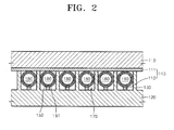
- FIG. 2 is a cross-sectional view taken along line II-II of FIG. 1.
- the PDP 100 includes a first substrate 110 and a second substrate 120 that oppose each other and are combined with each other.
- the first substrate 110 and the second substrate 120 are separated from each other by a predetermined gap and define red, green, and blue discharge cells 170 corresponding to red, green, and blue subpixels.
- the first substrate 111 and the second substrate 120 may be formed of a flexible material. Various flexible materials may be used.
- the first substrate 110 and the second substrate 120 may include silicon rubber, polydimethylsiloxane (PDMS) or polyester. However, the present embodiments are not limited to this and the first substrate 110 and the second substrate 120 may also be formed of glass.
- a plurality of discharge electrode pairs 115 in which a discharge occurs in discharge cells 170 are disposed between the first substrate 110 and the second substrate 120.
- Each discharge electrode pair 115 includes a first electrode 111 and a second electrode 112 which extend to cross each other. A detailed description thereof will now be described.
- First electrodes 111 are disposed on an inner side surface of the first substrate 110.
- the first electrodes 111 are separated from one another by a predetermined gap and extend to be parallel to one another.
- One first electrode 111 corresponds to each discharge cell 170, extends along a first direction (x direction) and has a striped shape.
- the first electrodes 111 may be formed, for example, of indium tin oxide (ITO) for visible rays transmission ratio improvement. Since, in ITO, a large voltage drop occurs in a lengthwise direction, an additional bus electrode may be disposed on the ITO.
- ITO indium tin oxide
- Second electrodes 112 are disposed on an inner side surface of the second substrate 120.
- the second electrodes 112 are separated from one another by a predetermined gap and extend to be parallel to one another.
- One second electrode 112 corresponds to each discharge cell 170, extends along a second direction (y direction) that crosses the first direction (x direction) and has a striped shape.
- the second electrodes 112 may be formed, for example, of indium tin oxide (ITO) for visible rays transmission ratio improvement.
- ITO indium tin oxide
- an additional bus electrode may be disposed on the ITO.
- the discharge cells 170 are partitioned by barrier ribs 130 interposed between the first substrate 110 and the second substrate 120.
- the barrier ribs 130 define a space in which shell structures 150 will be arranged. Referring to FIG. 1, the barrier ribs 130 have a striped shape that extends along the second direction (y direction).
- the discharge cells 170 are disposed in a matrix arrangement by the barrier ribs 130.
- the barrier ribs 130 may be separately formed independent of the first substrate 110 and the second substrate 120. However, for the convenience of manufacture, the barrier ribs 130 may be integrated with the first substrate 110 or the second substrate 120. In FIGS. 1 and 2, the barrier ribs 130 and the second substrate 120 are integrated into a single unit.
- the shell structures 150 are disposed inside the discharge cells 170.
- One shell structure 150 may be disposed in each discharge cell 170 or a plurality of shell structures 150 may be disposed in each discharge cell 170.
- Each shell structure 150 includes a shell 151, a discharge gas (not shown), and a phosphor layer 152.
- the shell 151 defines a space 180 in which a discharge occurs and has a spherical shape.
- a discharge gas is sealed in the space defined by the shell 151.
- the discharge gas may include an inert gas including Xe, Kr, Ne, Ar, and He or a mixture thereof or at least one of Hg, N 2 , and D 2 .
- the shell 151 seals the discharge gas and may be formed of a material including MgF 2 , MgO or Si 3 N 4 . Such materials have a high transmission ratio of UV rays generated by the discharge gas and stabilizing properties.
- the shell 151 may be formed of MgF 2 . This is because a UV rays transmission ratio of MgF 2 having a wavelength less than about 250 nm is higher through MgF 2 than other materials.
- the shell 151 may be formed of a material including MgF 2 , MgO or Si 3 N 4 having a high transmission ratio in a long wavelength region since UV rays generated by the discharge gas have a long wavelength greater than about 250 nm.
- Characteristics of the shell 151 and a method of manufacturing the same are disclosed in U.S Patent Nos. 6,669,961 , 6,073,578 , 6,060,128 , 5,948,483 , and 5,344,676 , and U.S Patent Application Publication Nos. 20050123614 , 20040022939 , and 20020054912 .
- Photos of a shell manufactured using MgF 2 are shown in FIGS. 3A and 3B.
- the shell 151 can be manufactured using micro sphere manufacturing technology disclosed in U.S. Patent No. 6,669,961 .
- the size of the shell 151 can have a diameter from about 1 micron ( ⁇ m) to about 1000 microns ( ⁇ m).
- Phosphor layers 152 producing red, green, and blue light are formed on an outer surface of the shell 151.
- the phosphor layers 152 include components that emit visible rays from ultraviolet (UV) rays.
- the phosphor layers 152 formed in red discharge cells include phosphor such as Y(V,P)O 4 :Eu
- the phosphor layers 152 formed in green discharge cells include phosphor such as Zn 2 SiO 4 :Mn
- the phosphor layers 152 formed in blue discharge cells include phosphor such as BAM:Eu.
- FIG. 4A a mould 180 having a shape in which the second substrate 120 and the barrier ribs 130 can be integrated into a single unit is prepared.
- liquid silicon rubber 181 is injected into the mould 180 in the vacuum state.
- FIG. 4B illustrates a state where the liquid silicon rubber 181 is injected into the mould 180.
- the silicon rubber 181 is a two-liquid type silicon rubber and formed by mixing a main agent and a hardener. Referring to FIG. 4B, first, the main agent and the hardener are mixed in the mould 180 at a ratio of approximately 10:1 and vapours in the mixture are sufficiently removed in the vacuum state. The process of removing vapours is performed under a vacuum chamber for about 40 minutes. At this time, the vacuum state should be maintained for a sufficient time so that any extra space is completely filled in a processed groove 180a.
- the silicon rubber 181 is solidified.
- the process of solidifying the silicon rubber 181 is performed in such a manner that the liquid silicon rubber 181 of which vapours are removed is cured at a hot air drying furnace of approximately 40°C for about one hour.
- the solidified silicon rubber 181 is removed from the mould 180, thereby manufacturing the second substrate 120 and the barrier ribs 130 to be integrated into a single unit.
- a resultant structure in which the second substrate 120 and the barrier ribs 130 are integrated into a single unit using the process is illustrated in FIG. 5.
- FIG. 4D illustrates a state where the second electrodes 112 are formed on the second substrate 120.
- a spherical shell 151 having a diameter from about 1 micron ( ⁇ m) to about 1000 microns ( ⁇ m) is manufactured in a chamber in which the discharge gas such as Xe is filled, using micro sphere manufacturing technology disclosed in U.S. Patent No. 6,669,961 by Kim, et al. issued December 30, 2003 .
- phosphor layers 152 are formed on an outer surface of the shell 151 using a spraying or dipping method. As shown in FIG.
- the mask 183 is disposed on the barrier ribs 130.
- the mask 183 has three shapes, so as to insert shell structures 150R, 150G, and 150B for red, green, and blue shell structures into the red, green, and blue discharge cells 170R, 170G, and 170B, respectively.
- the mask 183 illustrated in FIG. 4E is used for the shell structures 150R for emitting red light disposed in the red discharge cells 170B. Referring to FIG. 4E, an opening 183a is formed only in a portion of the mask 183 which corresponds to the red discharge cells 170R.
- each shell structure 150R for emitting red light includes a shell 151, a red light emitting phosphor layer 152R, and a discharge gas.
- the mask 183 of which opening 183a is formed in a position corresponding to the red or blue discharge cells 170G or 170B is disposed on the barrier ribs 130 so that the shell structures 150G for emitting green light and the shell structures 150B for emitting blue light are filled in the green discharge cells 170G and the blue discharge cells 170B, respectively.
- FIG. 4F illustrates a state where all of the shell structures 150R, 150G, and 150B are filled in each of the discharge cells 170R, 170G, and 170B.
- the resultant structure illustrated in FIG. 4F is combined with the inner surface of the first substrate 110 in which the first electrodes 111 are patterned.
- the first substrate 110 may be formed of silicon rubber. Since the first substrate 110, the second substrate 120, and the barrier ribs 130 have flexibility and buffering characteristics, when the first substrate 110 and the second substrate 120 are pressurized and combined with each other, the shell structures 150R, 150G, and 150B can be fixed in the discharge cells 170R, 170G, and 170B.
- An address voltage is applied between the first electrode 111 and the second electrode 112 so that an address discharge occurs.
- Discharge cells 170 in which a sustain discharge will occur as a result of the address discharge are selected.
- a sustain voltage is applied between the first electrode 111 and the second electrode 112 of the selected discharge cells 170, a sustain discharge occurs in the discharge space 180.
- the energy level of the excited discharge gas during the sustain discharge is reduced and UV rays are emitted.
- the UV rays excite the phosphor layers 152 coated on the outer side surface of the shell 151 after transmitting through the shell 151.
- the energy level of the excited phosphor layers 152 is reduced, visible rays are emitted, and the emitted visible rays constitute an image.
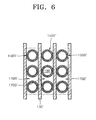
- FIG. 6 depicts a partially cross-sectional view of a modified example of the PDP 100 illustrated in FIG. 1.
- FIGS. 6 shows a plurality of shell structures 150R', 150G', and 150B' disposed in each of red, green, and blue discharge cells 170R', 170G', and 170B', which will now be described.
- the red, green, and blue discharge cells 170R', 170G', and 170B' are partitioned by stripe-shaped barrier ribs.
- the three red, green, and blue light emitting shell structures 150R', 150G', and 150B' are disposed in the red, green, and blue discharge cells 170R', 170G', and 170B', respectively.
- Detailed structure and functions of the red, green, and blue light emitting shell structures 150R', 150G', and 150B' are similar to the above description and thus will be omitted.
- the shell structures 150R', 150G', and 150B' may have a diameter from about 1 micron ( ⁇ m) to about 1000 microns ( ⁇ m).
- a space in the discharge cells can be more frequently used and defects that may occur in the shell structures can be reduced.
- FIG. 7 is a partially cutaway and exploded perspective view of the PDP 200
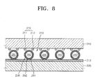
- FIG. 8 is a cross-sectional view taken along line VIII-VIII of FIG. 7.
- the first substrate 210 and the second substrate 220 are separated from each other by a predetermined gap and oppose each other.
- Barrier ribs 230 having a striped shape and partitioning a plurality of discharge cells 270 are disposed between the first substrate 210 and the second substrate 220.
- the barrier ribs 230 and the second substrate 220 are integrated into a single unit. Characteristics of the first substrate 210, the second substrate 220, and the barrier ribs 230 and a method of manufacturing the same are similar to those illustrated in FIG. 6 and thus will be omitted.
- a plurality of discharge electrode pairs 215 extends on the first substrate 210 that opposes the second substrate 220, to be parallel to one another.
- Each discharge electrode pair 215 corresponds to each discharge cell 270 and includes a first discharge electrode 211 and a second discharge electrode 212.
- Address electrodes 213 are disposed on the second substrate 220 that opposes the first substrate 210 and extend to cross the discharge electrode pairs 215.
- shell structures 250 are disposed inside the discharge cells 270.
- Each shell structure 250 includes a spherical shell 251, phosphor layers 252 coated on an outer surface of the shell 251, and a discharge gas filled in a discharge cell 280 inside the shell 251.
- one shell structure 250 corresponds to each discharge cell 270.
- the present embodiments are not limited to this and a plurality of shell structures 250 may be disposed in each discharge cell 270.
- the structure and function of the shell structure 250 are similar to those illustrated in FIG. 6 and thus will be omitted.
- An address voltage is applied between the first discharge electrode 211 and the address electrode 213 so that an address discharge occurs.
- Discharge cells 270 in which a sustain discharge will occur as a result of the address discharge are selected.
- a sustain voltage is applied between the first electrode 211 and the second electrode 212 of the selected discharge cells 270, a sustain discharge occurs in the discharge space 280.
- the energy level of the excited discharge gas during the sustain discharge is reduced and UV rays are emitted.
- the UV rays excite the phosphor layers 252 coated on the outer side surface of the shell 251 after transmitting through the shell 251.
- the energy level of the excited phosphor layers 252 is reduced, visible rays are emitted, and the emitted visible rays constitute an image.
- the PDP according to the present embodiments has the following effects. First, since an image is realized by arranging the shell structure having a diameter from about 1 micron ( ⁇ m) to about 1000 microns ( ⁇ m) in the discharge cells, the PDP can be simply manufactured to be highly precise and fine. In particular, a method of coating the phosphor layers is simple and a process of forming an additional dielectric layer is unnecessary.
- the PDP can be simply manufactured and has flexibility.
- the barrier ribs are formed using a moulding process, it is advantageous to make the PDP highly precise and fine.
Landscapes
- Physics & Mathematics (AREA)
- Engineering & Computer Science (AREA)
- Plasma & Fusion (AREA)
- Gas-Filled Discharge Tubes (AREA)
Abstract
Description
- The present invention relates to a plasma display panel (PDP), and more particularly, to a PDP having a new structure that can be easily manufactured.
- Plasma display panels (PDP) have recently replaced conventional cathode ray tube (CRT) display devices. In a PDP, a discharge gas is sealed between two substrates on which a plurality of discharge electrodes are formed, a discharge voltage is applied, and phosphor formed in a predetermined pattern by ultraviolet rays generated by the discharge voltage is excited whereby a desired image is obtained.
- In order to make the PDP highly precise and fine, a discharge space in which a discharge occurs should be very small. However, as the discharge space is reduced, a process of forming a phosphor layer in the discharge space cannot be easily performed. In addition, barrier ribs that partition the discharge space are generally formed using a sandblasting process. It is very difficult to manufacture highly precise and fine barrier ribs using the sandblasting process. Furthermore, the number of processes involved in manufacturing the PDP is very large, which increases manufacturing time and costs.
- Embodiments of the present invention provide a plasma display panel (PDP) having a new structure that can be easily manufactured.
- According to an aspect of the present embodiments, there is provided a plasma display panel including: a substrate; and a shell structure disposed on the substrate and having a shell and a discharge gas filled in the shell.
- According to another aspect of the present embodiments, there is provided a plasma display panel including: a first substrate and a second substrate separated from each other by a predetermined gap and opposing each other; barrier ribs disposed between the first substrate and the second substrate and partitioning a plurality of discharge cells; discharge electrode pairs causing a discharge in the discharge cells; and shell structures disposed inside the discharge cells and having a discharge gas filled in the shell.
- The above and other aspects and advantages of the present invention will become more apparent by describing in detail exemplary embodiments thereof with reference to the attached drawings in which:
- FIG. 1 is a partially cutaway and exploded perspective view of a plasma display panel (PDP) according to an embodiment;
- FIG. 2 is a cross-sectional view taken along line II-II of FIG. 1;
- FIGS. 3A and 3B show photos of a shell manufactured using MgF2;
- FIGS. 4A through 4G illustrate a method of manufacturing the PDP illustrated in FIG. 1;
- FIG. 5 shows a photo of a resultant structure in which a second substrate and barrier ribs are integrated into a single unit using the method illustrated in FIGS. 4A through 4G;
- FIG. 6 is a partially cross-sectional view of a modified example of the PDP illustrated in FIG. 1;
- FIG. 7 is a partially cutaway and exploded perspective view of a PDP according to another embodiment; and
- FIG. 8 is a cross-sectional view taken along line VIII-VIII of FIG. 7.
- Embodiments will now be described more fully with reference to the accompanying drawings, in which exemplary embodiments are shown. Like reference numerals denote like elements.
- FIGS. 1 and 2 illustrate a plasma display panel (PDP) 100 according to an embodiment. FIG. 1 is a partially cutaway and exploded perspective view of the
PDP 100, and FIG. 2 is a cross-sectional view taken along line II-II of FIG. 1. - The PDP 100 includes a
first substrate 110 and asecond substrate 120 that oppose each other and are combined with each other. Thefirst substrate 110 and thesecond substrate 120 are separated from each other by a predetermined gap and define red, green, andblue discharge cells 170 corresponding to red, green, and blue subpixels. Thefirst substrate 111 and thesecond substrate 120 may be formed of a flexible material. Various flexible materials may be used. Thefirst substrate 110 and thesecond substrate 120 may include silicon rubber, polydimethylsiloxane (PDMS) or polyester. However, the present embodiments are not limited to this and thefirst substrate 110 and thesecond substrate 120 may also be formed of glass. - A plurality of
discharge electrode pairs 115 in which a discharge occurs indischarge cells 170 are disposed between thefirst substrate 110 and thesecond substrate 120. Eachdischarge electrode pair 115 includes afirst electrode 111 and asecond electrode 112 which extend to cross each other. A detailed description thereof will now be described. -
First electrodes 111 are disposed on an inner side surface of thefirst substrate 110. Thefirst electrodes 111 are separated from one another by a predetermined gap and extend to be parallel to one another. Onefirst electrode 111 corresponds to eachdischarge cell 170, extends along a first direction (x direction) and has a striped shape. In addition, thefirst electrodes 111 may be formed, for example, of indium tin oxide (ITO) for visible rays transmission ratio improvement. Since, in ITO, a large voltage drop occurs in a lengthwise direction, an additional bus electrode may be disposed on the ITO. -
Second electrodes 112 are disposed on an inner side surface of thesecond substrate 120. Thesecond electrodes 112 are separated from one another by a predetermined gap and extend to be parallel to one another. Onesecond electrode 112 corresponds to eachdischarge cell 170, extends along a second direction (y direction) that crosses the first direction (x direction) and has a striped shape. In addition, thesecond electrodes 112 may be formed, for example, of indium tin oxide (ITO) for visible rays transmission ratio improvement. Like in thefirst electrodes 111, an additional bus electrode may be disposed on the ITO. - The
discharge cells 170 are partitioned bybarrier ribs 130 interposed between thefirst substrate 110 and thesecond substrate 120. Thebarrier ribs 130 define a space in whichshell structures 150 will be arranged. Referring to FIG. 1, thebarrier ribs 130 have a striped shape that extends along the second direction (y direction). Thedischarge cells 170 are disposed in a matrix arrangement by thebarrier ribs 130. Thebarrier ribs 130 may be separately formed independent of thefirst substrate 110 and thesecond substrate 120. However, for the convenience of manufacture, thebarrier ribs 130 may be integrated with thefirst substrate 110 or thesecond substrate 120. In FIGS. 1 and 2, thebarrier ribs 130 and thesecond substrate 120 are integrated into a single unit. - The
shell structures 150 are disposed inside thedischarge cells 170. Oneshell structure 150 may be disposed in eachdischarge cell 170 or a plurality ofshell structures 150 may be disposed in eachdischarge cell 170. Eachshell structure 150 includes ashell 151, a discharge gas (not shown), and aphosphor layer 152. Theshell 151 defines aspace 180 in which a discharge occurs and has a spherical shape. A discharge gas is sealed in the space defined by theshell 151. When voltage is applied to thefirst electrode 111 and thesecond electrode 112, a discharge occurs. The discharge gas may include an inert gas including Xe, Kr, Ne, Ar, and He or a mixture thereof or at least one of Hg, N2, and D2. - The
shell 151 seals the discharge gas and may be formed of a material including MgF2, MgO or Si3N4. Such materials have a high transmission ratio of UV rays generated by the discharge gas and stabilizing properties. In particular, theshell 151 may be formed of MgF2. This is because a UV rays transmission ratio of MgF2 having a wavelength less than about 250 nm is higher through MgF2 than other materials. When the discharge gas includes at least one of Hg, N2, and D2, theshell 151 may be formed of a material including MgF2, MgO or Si3N4 having a high transmission ratio in a long wavelength region since UV rays generated by the discharge gas have a long wavelength greater than about 250 nm. - Characteristics of the
shell 151 and a method of manufacturing the same are disclosed in U.S PatentNos. 6,669,961 ,6,073,578 ,6,060,128 ,5,948,483 , and5,344,676 , and U.S Patent Application PublicationNos. 20050123614 ,20040022939 , and20020054912 . Photos of a shell manufactured using MgF2 are shown in FIGS. 3A and 3B. Theshell 151 can be manufactured using micro sphere manufacturing technology disclosed inU.S. Patent No. 6,669,961 . The size of theshell 151 can have a diameter from about 1 micron (µm) to about 1000 microns (µm). - Phosphor layers 152 producing red, green, and blue light are formed on an outer surface of the
shell 151. The phosphor layers 152 include components that emit visible rays from ultraviolet (UV) rays. The phosphor layers 152 formed in red discharge cells include phosphor such as Y(V,P)O4:Eu, the phosphor layers 152 formed in green discharge cells include phosphor such as Zn2SiO4:Mn, and the phosphor layers 152 formed in blue discharge cells include phosphor such as BAM:Eu. - A method of manufacturing the
PDP 100 having the above structure will now be described with reference to FIGS. 4A through 4G. - Referring to FIG. 4A, a
mould 180 having a shape in which thesecond substrate 120 and thebarrier ribs 130 can be integrated into a single unit is prepared. Next,liquid silicon rubber 181 is injected into themould 180 in the vacuum state. FIG. 4B illustrates a state where theliquid silicon rubber 181 is injected into themould 180. Thesilicon rubber 181 is a two-liquid type silicon rubber and formed by mixing a main agent and a hardener. Referring to FIG. 4B, first, the main agent and the hardener are mixed in themould 180 at a ratio of approximately 10:1 and vapours in the mixture are sufficiently removed in the vacuum state. The process of removing vapours is performed under a vacuum chamber for about 40 minutes. At this time, the vacuum state should be maintained for a sufficient time so that any extra space is completely filled in a processedgroove 180a. - After that, the
silicon rubber 181 is solidified. The process of solidifying thesilicon rubber 181 is performed in such a manner that theliquid silicon rubber 181 of which vapours are removed is cured at a hot air drying furnace of approximately 40°C for about one hour. Next, referring to FIG. 4C, the solidifiedsilicon rubber 181 is removed from themould 180, thereby manufacturing thesecond substrate 120 and thebarrier ribs 130 to be integrated into a single unit. A resultant structure in which thesecond substrate 120 and thebarrier ribs 130 are integrated into a single unit using the process is illustrated in FIG. 5. - After the
second substrate 120 and thebarrier ribs 130 are manufactured, thesecond electrodes 112 are patterned on thesecond substrate 120. FIG. 4D illustrates a state where thesecond electrodes 112 are formed on thesecond substrate 120. - Next, a process of inserting the
shell structures 150 into the red, green, andblue discharge cells 170 using amask 183 is performed. A method of manufacturing theshell structures 150 will now be described. Aspherical shell 151 having a diameter from about 1 micron (µm) to about 1000 microns (µm) is manufactured in a chamber in which the discharge gas such as Xe is filled, using micro sphere manufacturing technology disclosed inU.S. Patent No. 6,669,961 by Kim, et al. issued December 30, 2003 . After that, phosphor layers 152 are formed on an outer surface of theshell 151 using a spraying or dipping method. As shown in FIG. 4E, aftershell structures 150R for red shell structures are formed, themask 183 is disposed on thebarrier ribs 130. Themask 183 has three shapes, so as to insertshell structures blue discharge cells mask 183 illustrated in FIG. 4E is used for theshell structures 150R for emitting red light disposed in thered discharge cells 170B. Referring to FIG. 4E, anopening 183a is formed only in a portion of themask 183 which corresponds to thered discharge cells 170R. In addition, eachshell structure 150R for emitting red light includes ashell 151, a red light emittingphosphor layer 152R, and a discharge gas. Thus, if all of theshell structures 150R for emitting red light are filled in thered discharge cells 170R, themask 183 of whichopening 183a is formed in a position corresponding to the red orblue discharge cells barrier ribs 130 so that theshell structures 150G for emitting green light and theshell structures 150B for emitting blue light are filled in thegreen discharge cells 170G and theblue discharge cells 170B, respectively. FIG. 4F illustrates a state where all of theshell structures discharge cells - Next, referring to FIG. 4G, the resultant structure illustrated in FIG. 4F is combined with the inner surface of the
first substrate 110 in which thefirst electrodes 111 are patterned. Thefirst substrate 110 may be formed of silicon rubber. Since thefirst substrate 110, thesecond substrate 120, and thebarrier ribs 130 have flexibility and buffering characteristics, when thefirst substrate 110 and thesecond substrate 120 are pressurized and combined with each other, theshell structures discharge cells - The operation of the
PDP 100 having the above structure according to the present embodiments will now be described. - An address voltage is applied between the
first electrode 111 and thesecond electrode 112 so that an address discharge occurs.Discharge cells 170 in which a sustain discharge will occur as a result of the address discharge are selected. After that, if a sustain voltage is applied between thefirst electrode 111 and thesecond electrode 112 of the selecteddischarge cells 170, a sustain discharge occurs in thedischarge space 180. The energy level of the excited discharge gas during the sustain discharge is reduced and UV rays are emitted. The UV rays excite the phosphor layers 152 coated on the outer side surface of theshell 151 after transmitting through theshell 151. The energy level of the excited phosphor layers 152 is reduced, visible rays are emitted, and the emitted visible rays constitute an image. - FIG. 6 depicts a partially cross-sectional view of a modified example of the
PDP 100 illustrated in FIG. 1. FIGS. 6 shows a plurality ofshell structures 150R', 150G', and 150B' disposed in each of red, green, andblue discharge cells 170R', 170G', and 170B', which will now be described. - The red, green, and
blue discharge cells 170R', 170G', and 170B' are partitioned by stripe-shaped barrier ribs. The three red, green, and blue light emittingshell structures 150R', 150G', and 150B' are disposed in the red, green, andblue discharge cells 170R', 170G', and 170B', respectively. Detailed structure and functions of the red, green, and blue light emittingshell structures 150R', 150G', and 150B' are similar to the above description and thus will be omitted. Theshell structures 150R', 150G', and 150B' may have a diameter from about 1 micron (µm) to about 1000 microns (µm). - As described above, since a plurality of shell structures are disposed in one discharge cell, a space in the discharge cells can be more frequently used and defects that may occur in the shell structures can be reduced.
- A
PDP 200 according to another embodiment will now be described with reference to FIGS. 7 and 8. FIG. 7 is a partially cutaway and exploded perspective view of thePDP 200, and FIG. 8 is a cross-sectional view taken along line VIII-VIII of FIG. 7. - The
first substrate 210 and thesecond substrate 220 are separated from each other by a predetermined gap and oppose each other.Barrier ribs 230 having a striped shape and partitioning a plurality ofdischarge cells 270 are disposed between thefirst substrate 210 and thesecond substrate 220. Thebarrier ribs 230 and thesecond substrate 220 are integrated into a single unit. Characteristics of thefirst substrate 210, thesecond substrate 220, and thebarrier ribs 230 and a method of manufacturing the same are similar to those illustrated in FIG. 6 and thus will be omitted. - A plurality of discharge electrode pairs 215 extends on the
first substrate 210 that opposes thesecond substrate 220, to be parallel to one another. Eachdischarge electrode pair 215 corresponds to eachdischarge cell 270 and includes afirst discharge electrode 211 and asecond discharge electrode 212.Address electrodes 213 are disposed on thesecond substrate 220 that opposes thefirst substrate 210 and extend to cross the discharge electrode pairs 215. - Referring to FIG. 8,
shell structures 250 are disposed inside thedischarge cells 270. Eachshell structure 250 includes aspherical shell 251, phosphor layers 252 coated on an outer surface of theshell 251, and a discharge gas filled in adischarge cell 280 inside theshell 251. Referring to FIG. 8, oneshell structure 250 corresponds to eachdischarge cell 270. However, the present embodiments are not limited to this and a plurality ofshell structures 250 may be disposed in eachdischarge cell 270. The structure and function of theshell structure 250 are similar to those illustrated in FIG. 6 and thus will be omitted. - An address voltage is applied between the
first discharge electrode 211 and theaddress electrode 213 so that an address discharge occurs.Discharge cells 270 in which a sustain discharge will occur as a result of the address discharge are selected. After that, if a sustain voltage is applied between thefirst electrode 211 and thesecond electrode 212 of the selecteddischarge cells 270, a sustain discharge occurs in thedischarge space 280. The energy level of the excited discharge gas during the sustain discharge is reduced and UV rays are emitted. The UV rays excite the phosphor layers 252 coated on the outer side surface of theshell 251 after transmitting through theshell 251. The energy level of the excited phosphor layers 252 is reduced, visible rays are emitted, and the emitted visible rays constitute an image. - The PDP according to the present embodiments has the following effects. First, since an image is realized by arranging the shell structure having a diameter from about 1 micron (µm) to about 1000 microns (µm) in the discharge cells, the PDP can be simply manufactured to be highly precise and fine. In particular, a method of coating the phosphor layers is simple and a process of forming an additional dielectric layer is unnecessary.
- Second, when the second substrate and the barrier ribs are integrated into a single unit using silicon rubber, the PDP can be simply manufactured and has flexibility. In particular, since the barrier ribs are formed using a moulding process, it is advantageous to make the PDP highly precise and fine.
- While the present invention has been particularly shown and described with reference to exemplary embodiments thereof, it will be understood by those of ordinary skill in the art that various changes in form and details may be made therein without departing from the scope of the present invention as defined by the following claims.
Claims (18)
- A plasma display panel comprising:a substrate; anda shell structure disposed on the substrate comprising a shell and a discharge gas within the shell.
- The plasma display panel of claim 1, wherein the shell comprises at least one material selected from the group consisting of MgF2, MgO, SiO2, and Si3N4.
- The plasma display panel of claim 1 or 2, wherein the discharge gas comprises an inert gas or at least one material selected from the group consisting of Hg, N2, and D2.
- The plasma display panel of claim 1, 2 or 3 wherein the shell structure further comprises phosphor layers disposed on an outer surface of the shell.
- The plasma display panel of any one of the preceding claims, wherein the substrate is a flexible substrate.
- The plasma display panel of claim 5, wherein the substrate comprises at least one material selected from the group consisting of silicon rubber, polydimethylsiloxane (PDMS), and polyester.
- The plasma display panel of any one of the preceding claims, wherein the shell structure is spherical.
- The plasma display panel of any one of the preceding claims, further comprising barrier ribs disposed on the substrate configured to define a space in which the shell structure is arranged.
- The plasma display panel of claim 8, wherein the barrier ribs and the substrate are integrated into a single unit.
- A plasma display panel according to claim 8 or 9, comprising:first and second opposing substrates separated from each other by a predetermined gap; whereinthe barrier ribs are disposed between the first substrate and the second substrate to partition a plurality of discharge cells; anda plurality of the shell structures are disposed inside the discharge cells, the plasma display panel further comprising:discharge electrode pairs configured to cause a discharge in the discharge cells.
- The plasma display panel of claim 10, wherein the first substrate or the second substrate and the barrier ribs are integrated into a single unit.
- The plasma display panel of claim 10 or 11, wherein at least one of the first substrate and the second substrate is a flexible substrate.
- The plasma display panel of claim 10, 11 or 12, wherein at least one of the first substrate and the second substrate comprises at least one material selected from the group consisting of silicon rubber, polydimethylsiloxane (PDMS), and polyester.
- The plasma display panel of any one of claims 10 to 13, wherein a plurality of the shell structures are disposed in each discharge cell.
- The plasma display panel of any one of claims 10 to 14, wherein each of the discharge electrode pairs comprises a first electrode and a second electrode that extend in directions that cross each other.
- The plasma display panel of claim 15, wherein the first electrode is disposed on the first substrate and the second electrode is disposed on the second substrate.
- The plasma display panel of any one of claims 10 to 14, wherein each of the discharge electrode pairs comprises a first electrode and a second electrode that extend parallel to each other.
- The plasma display panel of claim 17, wherein each of the discharge electrode pairs further comprises address electrodes that extend in a direction that crosses the direction of the first electrode and the second electrode.
Applications Claiming Priority (1)
| Application Number | Priority Date | Filing Date | Title |
|---|---|---|---|
| KR1020050103460A KR20070046613A (en) | 2005-10-31 | 2005-10-31 | Plasma display panel |
Publications (2)
| Publication Number | Publication Date |
|---|---|
| EP1780750A2 true EP1780750A2 (en) | 2007-05-02 |
| EP1780750A3 EP1780750A3 (en) | 2008-07-30 |
Family
ID=37606999
Family Applications (1)
| Application Number | Title | Priority Date | Filing Date |
|---|---|---|---|
| EP06123191A Withdrawn EP1780750A3 (en) | 2005-10-31 | 2006-10-30 | Plasma display panel |
Country Status (3)
| Country | Link |
|---|---|
| US (1) | US20070096650A1 (en) |
| EP (1) | EP1780750A3 (en) |
| KR (1) | KR20070046613A (en) |
Citations (2)
| Publication number | Priority date | Publication date | Assignee | Title |
|---|---|---|---|---|
| WO2002075706A2 (en) | 2000-10-27 | 2002-09-26 | Science Applications International Corporation | A socket for use with a micro-component in a light-emitting panel |
| US6919685B1 (en) | 2001-01-09 | 2005-07-19 | Imaging Systems Technology Inc | Microsphere |
Family Cites Families (2)
| Publication number | Priority date | Publication date | Assignee | Title |
|---|---|---|---|---|
| US6864631B1 (en) * | 2000-01-12 | 2005-03-08 | Imaging Systems Technology | Gas discharge display device |
| JP4181862B2 (en) * | 2002-11-28 | 2008-11-19 | 篠田プラズマ株式会社 | Arc tube array type display device |
-
2005
- 2005-10-31 KR KR1020050103460A patent/KR20070046613A/en not_active Ceased
-
2006
- 2006-09-20 US US11/524,616 patent/US20070096650A1/en not_active Abandoned
- 2006-10-30 EP EP06123191A patent/EP1780750A3/en not_active Withdrawn
Patent Citations (2)
| Publication number | Priority date | Publication date | Assignee | Title |
|---|---|---|---|---|
| WO2002075706A2 (en) | 2000-10-27 | 2002-09-26 | Science Applications International Corporation | A socket for use with a micro-component in a light-emitting panel |
| US6919685B1 (en) | 2001-01-09 | 2005-07-19 | Imaging Systems Technology Inc | Microsphere |
Also Published As
| Publication number | Publication date |
|---|---|
| US20070096650A1 (en) | 2007-05-03 |
| KR20070046613A (en) | 2007-05-03 |
| EP1780750A3 (en) | 2008-07-30 |
Similar Documents
| Publication | Publication Date | Title |
|---|---|---|
| KR100662061B1 (en) | Method of manufacturing plasma display panel and substrate structure | |
| KR100471980B1 (en) | Plasma display panel having barrier and manufacturing method of the barrier | |
| CN100446161C (en) | plasma display | |
| US6646376B2 (en) | Plasma display panel and a plasma display panel production method | |
| KR20000009132A (en) | Manufacturing method of separating wall for plasma display panel and plasma display panel device using it | |
| JP2001357784A (en) | Surface discharge type display device | |
| US20100133974A1 (en) | Plasma display panel | |
| US20070096650A1 (en) | Plasma display panel | |
| WO2003075301A1 (en) | Plasma display | |
| CN100521040C (en) | Plasma display panel manufacturing method | |
| US20090058298A1 (en) | Plasma display panel and method of fabricating the same | |
| US7482748B2 (en) | Plasma display panel with paste composite for white-black formation | |
| KR100502908B1 (en) | Plasma display panel and manufacturing method thereof | |
| US20080054789A1 (en) | Plasma display panel (PDP) | |
| US20080018249A1 (en) | Plasma display panel and production process of same | |
| US20050017640A1 (en) | Plasma display panel and fabrication method thereof | |
| KR100766945B1 (en) | Plasma dispaly panel and manufacturing method of the same | |
| KR100925093B1 (en) | Plasma display panel manufacturing method | |
| KR100766021B1 (en) | Plasma Display Panel With Paper Partition And Manufacturing Method Thereof | |
| JP2006156349A (en) | Plasma display panel | |
| KR100696634B1 (en) | Gas discharge display device and manufacturing method thereof | |
| US20100096973A1 (en) | Plasma display panel and method of manufacturing the same | |
| KR100749164B1 (en) | Partition Wall Formation Method of Display Panel Using Discharge | |
| KR100293511B1 (en) | Bulkhead composition and bulkhead manufacturing method for plasma display device | |
| KR100565207B1 (en) | Plasma Display Panel And Method Of Manufacturing The Same |
Legal Events
| Date | Code | Title | Description |
|---|---|---|---|
| PUAI | Public reference made under article 153(3) epc to a published international application that has entered the european phase |
Free format text: ORIGINAL CODE: 0009012 |
|
| 17P | Request for examination filed |
Effective date: 20061030 |
|
| AK | Designated contracting states |
Kind code of ref document: A2 Designated state(s): AT BE BG CH CY CZ DE DK EE ES FI FR GB GR HU IE IS IT LI LT LU LV MC NL PL PT RO SE SI SK TR |
|
| AX | Request for extension of the european patent |
Extension state: AL BA HR MK YU |
|
| PUAL | Search report despatched |
Free format text: ORIGINAL CODE: 0009013 |
|
| AK | Designated contracting states |
Kind code of ref document: A3 Designated state(s): AT BE BG CH CY CZ DE DK EE ES FI FR GB GR HU IE IS IT LI LT LU LV MC NL PL PT RO SE SI SK TR |
|
| AX | Request for extension of the european patent |
Extension state: AL BA HR MK RS |
|
| AKX | Designation fees paid |
Designated state(s): DE FR GB |
|
| RAP1 | Party data changed (applicant data changed or rights of an application transferred) |
Owner name: SAMSUNG SDI CO., LTD. |
|
| 17Q | First examination report despatched |
Effective date: 20091221 |
|
| STAA | Information on the status of an ep patent application or granted ep patent |
Free format text: STATUS: THE APPLICATION IS DEEMED TO BE WITHDRAWN |
|
| 18D | Application deemed to be withdrawn |
Effective date: 20100701 |