EP1778897B1 - Structure comprising iii-nitride materials including low dislocation densities and method of its formation - Google Patents
Structure comprising iii-nitride materials including low dislocation densities and method of its formation Download PDFInfo
- Publication number
- EP1778897B1 EP1778897B1 EP05768527.3A EP05768527A EP1778897B1 EP 1778897 B1 EP1778897 B1 EP 1778897B1 EP 05768527 A EP05768527 A EP 05768527A EP 1778897 B1 EP1778897 B1 EP 1778897B1
- Authority
- EP
- European Patent Office
- Prior art keywords
- nitride material
- iii
- material region
- layer
- strain
- Prior art date
- Legal status (The legal status is an assumption and is not a legal conclusion. Google has not performed a legal analysis and makes no representation as to the accuracy of the status listed.)
- Not-in-force
Links
Images


Classifications
-
- C—CHEMISTRY; METALLURGY
- C30—CRYSTAL GROWTH
- C30B—SINGLE-CRYSTAL GROWTH; UNIDIRECTIONAL SOLIDIFICATION OF EUTECTIC MATERIAL OR UNIDIRECTIONAL DEMIXING OF EUTECTOID MATERIAL; REFINING BY ZONE-MELTING OF MATERIAL; PRODUCTION OF A HOMOGENEOUS POLYCRYSTALLINE MATERIAL WITH DEFINED STRUCTURE; SINGLE CRYSTALS OR HOMOGENEOUS POLYCRYSTALLINE MATERIAL WITH DEFINED STRUCTURE; AFTER-TREATMENT OF SINGLE CRYSTALS OR A HOMOGENEOUS POLYCRYSTALLINE MATERIAL WITH DEFINED STRUCTURE; APPARATUS THEREFOR
- C30B29/00—Single crystals or homogeneous polycrystalline material with defined structure characterised by the material or by their shape
- C30B29/10—Inorganic compounds or compositions
- C30B29/40—AIIIBV compounds wherein A is B, Al, Ga, In or Tl and B is N, P, As, Sb or Bi
- C30B29/403—AIII-nitrides
-
- C—CHEMISTRY; METALLURGY
- C30—CRYSTAL GROWTH
- C30B—SINGLE-CRYSTAL GROWTH; UNIDIRECTIONAL SOLIDIFICATION OF EUTECTIC MATERIAL OR UNIDIRECTIONAL DEMIXING OF EUTECTOID MATERIAL; REFINING BY ZONE-MELTING OF MATERIAL; PRODUCTION OF A HOMOGENEOUS POLYCRYSTALLINE MATERIAL WITH DEFINED STRUCTURE; SINGLE CRYSTALS OR HOMOGENEOUS POLYCRYSTALLINE MATERIAL WITH DEFINED STRUCTURE; AFTER-TREATMENT OF SINGLE CRYSTALS OR A HOMOGENEOUS POLYCRYSTALLINE MATERIAL WITH DEFINED STRUCTURE; APPARATUS THEREFOR
- C30B25/00—Single-crystal growth by chemical reaction of reactive gases, e.g. chemical vapour-deposition growth
- C30B25/02—Epitaxial-layer growth
-
- H—ELECTRICITY
- H01—ELECTRIC ELEMENTS
- H01L—SEMICONDUCTOR DEVICES NOT COVERED BY CLASS H10
- H01L21/00—Processes or apparatus adapted for the manufacture or treatment of semiconductor or solid state devices or of parts thereof
- H01L21/02—Manufacture or treatment of semiconductor devices or of parts thereof
- H01L21/02104—Forming layers
- H01L21/02365—Forming inorganic semiconducting materials on a substrate
- H01L21/02367—Substrates
- H01L21/0237—Materials
- H01L21/02373—Group 14 semiconducting materials
- H01L21/02381—Silicon, silicon germanium, germanium
-
- H—ELECTRICITY
- H01—ELECTRIC ELEMENTS
- H01L—SEMICONDUCTOR DEVICES NOT COVERED BY CLASS H10
- H01L21/00—Processes or apparatus adapted for the manufacture or treatment of semiconductor or solid state devices or of parts thereof
- H01L21/02—Manufacture or treatment of semiconductor devices or of parts thereof
- H01L21/02104—Forming layers
- H01L21/02365—Forming inorganic semiconducting materials on a substrate
- H01L21/02436—Intermediate layers between substrates and deposited layers
- H01L21/02439—Materials
- H01L21/02455—Group 13/15 materials
- H01L21/02458—Nitrides
-
- H—ELECTRICITY
- H01—ELECTRIC ELEMENTS
- H01L—SEMICONDUCTOR DEVICES NOT COVERED BY CLASS H10
- H01L21/00—Processes or apparatus adapted for the manufacture or treatment of semiconductor or solid state devices or of parts thereof
- H01L21/02—Manufacture or treatment of semiconductor devices or of parts thereof
- H01L21/02104—Forming layers
- H01L21/02365—Forming inorganic semiconducting materials on a substrate
- H01L21/02436—Intermediate layers between substrates and deposited layers
- H01L21/02439—Materials
- H01L21/02488—Insulating materials
-
- H—ELECTRICITY
- H01—ELECTRIC ELEMENTS
- H01L—SEMICONDUCTOR DEVICES NOT COVERED BY CLASS H10
- H01L21/00—Processes or apparatus adapted for the manufacture or treatment of semiconductor or solid state devices or of parts thereof
- H01L21/02—Manufacture or treatment of semiconductor devices or of parts thereof
- H01L21/02104—Forming layers
- H01L21/02365—Forming inorganic semiconducting materials on a substrate
- H01L21/02436—Intermediate layers between substrates and deposited layers
- H01L21/02494—Structure
- H01L21/02496—Layer structure
- H01L21/02505—Layer structure consisting of more than two layers
-
- H—ELECTRICITY
- H01—ELECTRIC ELEMENTS
- H01L—SEMICONDUCTOR DEVICES NOT COVERED BY CLASS H10
- H01L21/00—Processes or apparatus adapted for the manufacture or treatment of semiconductor or solid state devices or of parts thereof
- H01L21/02—Manufacture or treatment of semiconductor devices or of parts thereof
- H01L21/02104—Forming layers
- H01L21/02365—Forming inorganic semiconducting materials on a substrate
- H01L21/02436—Intermediate layers between substrates and deposited layers
- H01L21/02494—Structure
- H01L21/02496—Layer structure
- H01L21/0251—Graded layers
-
- H—ELECTRICITY
- H01—ELECTRIC ELEMENTS
- H01L—SEMICONDUCTOR DEVICES NOT COVERED BY CLASS H10
- H01L21/00—Processes or apparatus adapted for the manufacture or treatment of semiconductor or solid state devices or of parts thereof
- H01L21/02—Manufacture or treatment of semiconductor devices or of parts thereof
- H01L21/02104—Forming layers
- H01L21/02365—Forming inorganic semiconducting materials on a substrate
- H01L21/02436—Intermediate layers between substrates and deposited layers
- H01L21/02494—Structure
- H01L21/02513—Microstructure
-
- H—ELECTRICITY
- H01—ELECTRIC ELEMENTS
- H01L—SEMICONDUCTOR DEVICES NOT COVERED BY CLASS H10
- H01L21/00—Processes or apparatus adapted for the manufacture or treatment of semiconductor or solid state devices or of parts thereof
- H01L21/02—Manufacture or treatment of semiconductor devices or of parts thereof
- H01L21/02104—Forming layers
- H01L21/02365—Forming inorganic semiconducting materials on a substrate
- H01L21/02518—Deposited layers
- H01L21/02521—Materials
- H01L21/02538—Group 13/15 materials
- H01L21/0254—Nitrides
-
- H—ELECTRICITY
- H01—ELECTRIC ELEMENTS
- H01L—SEMICONDUCTOR DEVICES NOT COVERED BY CLASS H10
- H01L21/00—Processes or apparatus adapted for the manufacture or treatment of semiconductor or solid state devices or of parts thereof
- H01L21/02—Manufacture or treatment of semiconductor devices or of parts thereof
- H01L21/02104—Forming layers
- H01L21/02365—Forming inorganic semiconducting materials on a substrate
- H01L21/02518—Deposited layers
- H01L21/02521—Materials
- H01L21/02538—Group 13/15 materials
- H01L21/02543—Phosphides
Definitions
- the invention relates generally to III-nitride materials and, more particularly, to III-nitride (e.g., gallium nitride) material structures including low dislocation densities, as well as methods associated with the same.
- III-nitride e.g., gallium nitride
- III-nitride materials include gallium nitride (GaN), aluminum nitride (AlN), indium nitride (InN) and their respective alloys (e.g., AlGaN, InGaN, AlInGaN and AlInN).
- gallium nitride materials GaN and its alloys
- have attractive properties including the ability to efficiently emit blue light, the ability to transmit signals at high frequency, and others. Accordingly, gallium nitride materials are being widely investigated in many microelectronic applications such as transistors, field emitters, and optoelectronic devices.
- III-nitride materials e.g., AlN
- Such layers may function as buffer or intermediate layers positioned between a substrate and an overlying gallium nitride material region.
- III-nitride materials have different crystal structures and properties than many common substrates including silicon, silicon carbide and sapphire. Thus, when III-nitride materials are formed on such substrates, these differences may lead to the formation of defects including dislocations. For example, dislocations may result from differences between the lattice constants of the substrate and the III-nitride material; differences between the thermal expansion coefficients of the substrate and the III-nitride material; as well as, substrate quality including misorientation and defects.
- Dislocations are linear imperfections in a crystalline array of atoms. Types of dislocations include edge dislocations, screw dislocations and mixed dislocations (which have an edge component and a screw component).
- edge dislocations include edge dislocations, screw dislocations and mixed dislocations (which have an edge component and a screw component).
- the dislocations can function as scattering centers which effect electron transport and, thus, impair electrical performance.
- the dislocations can function as non-radiative recombination centers which reduce performance of opto-electronic devices.
- dislocations can lead to inhomogeneities in composition and formation of macro-defects which can also negatively effect device performance.
- Certain conventional vertical growth processes (i.e., growth that proceeds in a vertical direction from the underlying layer) form III-nitride material regions having screw dislocation densities of greater than about 10 12 /cm 3 . Lateral growth processes can produce localized areas within III-nitride material regions having low defect densities, while other areas within the regions have relatively high defect densities. Lateral growth processes are typically more complex than vertical growth processes.
- JP 9134878 A describes forming a thin film of gallium having a thickness of about 50 nm or less on a silicon substrate.
- a nitride layer is formed on the thin film using metal organic chemical vapour deposition (MOCVD) and a GaN crystal is grown on the nitride layer by MOCVD.
- MOCVD metal organic chemical vapour deposition
- US 2004 021147 A describes a GaN-based ultraviolet light emitting diode.
- An undoped GaN seed crystal is grown on a sapphire substrate by metalorganic vapor phase epitaxy (MOVPE).
- MOVPE metalorganic vapor phase epitaxy
- SiO 2 is deposited and processed to form dielectric masks with a stripped pattern.
- undoped GaN is re-grown by epitaxial lateral overgrowth from starting points at portions of the seed crystal that are exposed through the dielectric masks.
- III-nitride materials having low dislocation e.g., screw dislocation
- densities including structures, devices and methods associated with the materials.
- a semiconductor structure comprising a substrate, a silicon nitride-based strain absorbing layer formed on the substrate, a III-nitride material region formed on the strain-absorbing layer, wherein a cross sectional area of the III-nitride material region greater than or equal to approximately 100 square microns and less than approximately 100 nm from a bottom surface of the III-nitride material region has a screw dislocation density of less than about 10 8 /cm 2 and an edge dislocation density of greater than about 10 8 /cm 2 and a second III-nitride material region formed on the III-nitride material region, wherein a cross sectional area of the second III-nitride material region greater than or equal to approximately 100 square microns and less than approximately 100 nm from a bottom surface of the second III-nitride material region has a screw dislocation density of less than 10 8 /cm 2.
- a semiconductor structure comprising a III-nitride material region including an area having dimensions of at least about 100 microns x 100 microns and a screw dislocation density of less than about 10 4 /cm 2 .
- a semiconductor structure in another example, comprises a semiconductor region having a top surface; and, a III-nitride material region formed over the top surface and having a different composition than the semiconductor region.
- a cross-sectional area of the III-nitride material region within 100 nanometers of the top surface has a screw dislocation density of less than about 10 8 /cm 2 .
- a semiconductor structure in another example, comprises a III-nitride material region having a screw dislocation density of less than about 10 8 /cm 2 and an edge dislocation density of greater than about 10 8 /cm 2 .
- a semiconductor structure in another example, comprises a III-nitride material region having an edge dislocation density and a screw dislocation density.
- the edge dislocation density is at least 100 times greater than the screw dislocation density.
- a semiconductor structure comprising a substrate, and a silicon nitride-based material layer having a thickness of less than 100 Angstroms and substantially covering an entire top surface of the substrate.
- the structure further comprises a III-nitride material region formed over the silicon nitride-based material layer and having a screw dislocation density of less than about 10 8 /cm 2 .
- a method of forming a semiconductor structure comprises providing a substrate; forming a silicon nitride-based strain absorbing layer on the substrate; vertically growing a III-nitride material region on the strain-absorbing layer, wherein a cross sectional area of the III-nitride material region greater than or equal to approximately 100 square microns and less than approximately 100 nm from a bottom surface of the III-nitride material region has a screw dislocation density of less than about 10 8 /cm 2 and an edge dislocation density of greater than about 10 8 /cm 2 ; and, vertically growing a second III- nitride material region over the III-nitride material region, wherein a cross sectional area of the second III-nitride material region greater than or equal to approximately 100 square microns and less than approximately 100 nm from a bottom surface of the second III -nitride material region has a screw dislocation density of less than about 10 8 /cm 2
- a method of forming a semiconductor structure comprises providing a semiconductor material region having a top surface; and, vertically growing a III-nitride material region over the semiconductor material region.
- the III-nitride material region has a composition different than the semiconductor material region.
- a screw dislocation density in a cross-sectional area of the III-nitride material region located within 100 nanometers of the top surface of the semiconductor material region is less than about 10 8 /cm 2 .
- the invention provides semiconductor structures including one or more III-nitride material region(s) (e.g., a gallium nitride material region) and methods associated with such structures.
- the III-nitride material region(s) advantageously have a low dislocation density and, in particular, a low screw dislocation density.
- the presence of screw dislocations in the III-nitride material region(s) may be essentially eliminated.
- the presence of a strain-absorbing layer underlying the III-nitride material region(s), amongst other factors can contribute to achieving the low screw dislocation densities.
- the III-nitride material region(s) having low dislocation densities include a gallium nitride material region which functions as the active region of the device.
- the low screw dislocation densities of the active device region e.g., gallium nitride material region
- improved properties e.g., electrical and optical
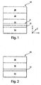
- FIG. 1 illustrates a semiconductor structure 10 according to one embodiment of the invention.
- the semiconductor structure includes a strain-absorbing layer 12 formed on a substrate 14.
- a series of III-nitride material regions are formed on the strain-absorbing layer.
- the series of III-nitride material regions includes an intermediate layer 15, a transition layer 16 and a gallium nitride material region 18.
- the strain-absorbing layer (amongst other factors) may help contribute to limiting generation of screw dislocation densities in at least one (and, in some cases, all) of the overlying III-nitride layers and, in particular, in the gallium nitride material region.
- Semiconductor structures of the invention may form the basis of a number of semiconductor devices including transistors (e.g., FET), Schottky diodes, light emitting diodes and laser diodes, amongst others.
- a layer When a layer is referred to as being “on” or “over” another layer or substrate, it can be directly on the layer or substrate, or an intervening layer also may be present. A layer that is “directly on” another layer or substrate means that no intervening layer is present. It should also be understood that when a layer is referred to as being “on” or “over” another layer or substrate, it may cover the entire layer or substrate, or a portion of the layer or substrate.
- III-nitride material refers to any Group III element-nitride compound including boron nitride (BN), aluminum nitride (AlN), gallium nitride (GaN), indium nitride (InN) and thalium nitride (TIN), as well as any alloys including Group III elements and Group V elements (e.g., Al x Ga (1-x) N, Al x In y Ca (1-x-y) N, In y Ga (1-y) N Al y In (1-y) N, GaAs a P b N( 1-a-b ), Al x In y Ga (1-x-y) AS a P b N (1-a-b) and the like). Typically, when present, arsenic and/or phosphorous are at low concentrations (i.e., less than 5 weight percent). III-nitride materials may be doped n-type or p-type, or may be intrinsic
- gallium nitride material refers to gallium nitride (GaN) and any of its alloys, such as aluminum gallium nitride (Al x Ga (1-x) N), indium gallium nitride (In y Ga (1-y) N), aluminum indium gallium nitride (Al x In y Ga (1-x-y) N), gallium arsenide phosporide nitride (GaAs a P b N (1-a-b) ), aluminum indium gallium arsenide phosporide nitride (Al x In y Ga (1-x-y) As a P b N (1-a-b) ), amongst others.
- Gallium nitride materials may be doped n-type or p-type, or may be intrinsic. Suitable gallium nitride materials have been described in commonly-owned U.S. Patent No. 6,649,287 which is incorporated herein by reference.
- region may refer to one layer (e.g., layer 15, layer 16) or may refer to a series of layers (e.g., gallium nitride material region 18 including layers 18a, 18b, 18c).
- At least one of the III-nitride material regions (e.g., intermediate layer 15, transition layer 16, gallium nitride material region 18) formed on the strain-absorbing layer has low screw dislocation densities.
- the screw dislocation density in one (or more) of the III-nitride material regions above the strain-absorbing layer is less than about 10 8 screw dislocations/cm 2 , and, in some cases, less than about 10 6 /cm 2 . It is even possible to achieve significantly lower screw dislocation densities within the scope of the present invention.
- one (or more) of the III-nitride material regions have very low screw dislocation densities of less than about 10 4 /cm 2 and, in some cases, less than about 10 2 /cm 2 . In some embodiments, it is even possible for one (or more) of the III-nitride material regions to have substantially zero screw dislocations.
- units for screw dislocation density may be expressed as "screw dislocations/cm 2 " or "/cm 2 ".
- At least the gallium nitride material region has the low screw dislocation density values noted above.
- the specific screw dislocation density depends, in part, on the particular structure including factors such as the thickness, composition and crystal structure of the strain-absorbing layer; the composition, thickness and crystal structure of the overlying III-nitride material layer(s)/region(s); as well as, the composition, thickness, and crystal structure of the substrate, amongst other factors.
- Screw dislocation densities may be measured using known techniques.
- a diffraction contrast technique e.g., g-vector analysis
- TEM transmission electron microscope
- the screw dislocation densities described herein are measured over a representative area.
- the representative area may depend, in part, on the actual dislocation density being measured. For example, a representative area of about 100 microns squared (e.g., 10 micron x 10 micron) may be suitable for measuring screw dislocation densities on the order of 10 8 /cm 2 . Larger representative areas may be used for smaller screw dislocation densities.
- the above-identified screw dislocation density ranges are present throughout one (or more) of the respective III-nitride material region(s) overlying the stress-absorbing layer. That is, throughout the entire volume of at least one (or more) of the III-nitride material region(s), the screw dislocation densities ranges identified above may be achieved.
- all of the III-nitride material regions e.g., intermediate layer 15, a transition layer 16 and a gallium nitride material region 18 formed over the strain-absorbing layer have the above-identified screw dislocation densities.
- the low screw dislocation densities are also achievable across large areas of III-nitride material regions.
- the above-identified screw dislocation densities may be found in regions having an area of greater than about 10 4 square microns; or, greater than about 1 mm 2 .
- the areas of the III-nitride material regions having the low screw dislocation densities may be greater than about 1 cm 2 , or more.
- the above-noted areas may comprises a variety of dimensions (i.e., lengths, widths) including similar lengths and widths.
- the above-identified screw dislocation densities may be found in areas having dimensions of greater than about 100 microns x 100 microns; or, greater than about 1 mm x I mm.
- the areas of the III-nitride material regions having the low screw dislocation densities may have dimensions of greater than about 1 cm x 1 cm, or more.
- the consistently low screw dislocation densities across large areas and/or throughout the entire region(s) provides advantages over certain prior art techniques (e.g., certain lateral growth processes) that form, within a respective III-nitride material region, areas of low screw dislocation density and also areas of high screw dislocation density (e.g., greater than 10 8 /cm 2 ).
- the III-nitride material region may have a substantially constant screw dislocation density throughout the entire region and/or area.
- the screw dislocation density is substantially constant along an axial direction (i.e., z-axis in FIG. 1 ) and is also substantially constant along a radial direction (i.e., x-axis in FIG. 1 ).
- the above-identified screw dislocation densities are achievable within areas of the III-nitride material region proximate to (e.g., within 100 nanometers, or within 50 nanometers) an underlying semiconductor region (e.g., substrate or semiconductor layer) formed of a different material composition.
- the area for example, is a cross-sectional area (e.g., A, in FIG. 1 ) of the III-nitride material region within 100 nanometers (or, within 50 nanometers) of the upper surface of the underlying region.
- the cross-sectional area may extend across the III-nitride region and may be parallel to the lower surface of the III-nitride material region (or the upper surface of the underlying region).
- the cross-sectional area may have any of the area values described above.
- the cross-sectional area and the III-nitride material region may be directly above the underlying semiconductor region, as shown.
- strain-absorbing layer 12 (with a thickness of less than 100 nanometers) may be formed between the III-nitride material region and the underlying semiconductor region (e.g., substrate 14).
- above-identified screw dislocation densities are achievable within an area of the III-nitride material region formed within 100 nanometers (or, 50 nanometers) of the top surface of a substrate having a different material composition than the III-nitride material region.
- the substrate may be formed of silicon, silicon carbide, sapphire (or, other substrate materials described below that meet this condition).
- the III-nitride material region may be intermediate layer 15, transition layer 16 or gallium nitride material region 18, depending on the structure.
- above-identified screw dislocation densities are achievable in a III-nitride material region formed within 100 nanometers (or, 50 nanometers) of the top surface of a semiconductor layer (i.e., non-substrate) having a different material composition than the III-nitride material region.
- the semiconductor material layer may be formed of a III-nitride material having a different composition than the III-nitride material region.
- the mechanism for limiting/eliminating screw dislocations in structures of the present invention may not have as significant an effect on lowering the edge dislocation density or mixed dislocation density.
- the edge dislocation density and/or mixed dislocation density may be greater than about 10 8 /cm 2 in the III-nitride material region having the reduced screw dislocation density.
- the edge dislocation density and/or mixed dislocation density is at least 100 times, or at least 10 4 times, greater than the screw dislocation density in the III-nitride material region.
- the edge dislocation density and/or mixed dislocation density may be at least 10 6 , or at least 10 8 times, the screw dislocation density in the III-nitride material region. In embodiments that do not have low edge and/or mixed dislocation densities, it should be understood that the structures still have the above-identified advantages associated with lower screw dislocation densities.
- edge and mixed dislocation densities may be achieved. It also should be understood that the above-referenced edge dislocation densities may be present throughout the III-nitride material region(s) and, at least, in the same portions of the III-nitride material region(s) having reduced screw dislocation densities.
- the low screw dislocation densities are achieved, at least in part, by the presence of the strain-absorbing layer.
- the III-nitride material regions may also have the low screw dislocation densities.
- Other factors include the composition, thickness and crystal structure of the intermediate layer, transition layer and III-nitride material region; the composition, thickness, and crystal structure of the substrate; and, process conditions described further below, amongst other factors.
- the composition, thickness and crystal structure of the strain-absorbing layer may contribute to reducing the formation of screw dislocations in the overlying III-nitride material layer(s)/region.
- the strain-absorbing layer may also reduce the formation of misfit dislocations in the layer formed on in the gallium nitride material region as described in commonly-owned, co-pending U.S. patent application publication number US2005/0285141 A1, filed June 28, 2004 , entitled "Gallium Nitride Materials and Methods Associated with the Same” which is incorporated herein by reference.
- Strain-absorbing layer 12 helps absorb strain that arises due to lattice differences between the crystal structure of the substrate and the crystal structure of layer/region formed on the strain-absorbing layer (e.g., intermediate layer 15 in FIG. 1 ; transition layer 16 in FIG. 2 ; and gallium nitride material region in FIG. 3 ). In the absence of the strain-absorbing layer, this strain is typically accommodated by the generation of misfit dislocations in the intermediate layer (or, other overlying layer) at the interface with the substrate. Thus, by providing an alternative mechanism for accommodating stress, the presence of the strain-absorbing layer may reduce the generation of misfit dislocations at the interface with the substrate. It is believed that the reduction in misfit dislocations can also lead to a reduction in screw dislocations in the overlying layers (e.g., intermediate layer 15, transition layer 16 and gallium nitride material region 18).
- the overlying layers e.g., intermediate layer 15, transition layer 16 and gallium nitride material region 18
- the strain-absorbing layer can help absorb strain that arises due to differences in the thermal expansion rate of the substrate as compared to the thermal expansion rate of the intermediate layer and/or the gallium nitride material region. Such differences can lead to formation of misfit dislocations at the intermediate layer/substrate interface, or cracking in either the intermediate layer and/or gallium nitride material region. As described further below, transition layer 16 also helps absorb this thermally-induced strain.
- strain-absorbing layer 12 is formed of a silicon nitride-based material.
- Silicon nitride-based materials include any silicon nitride-based compound (e.g., Si x N y , such as SiN and Si 3 N 4 , SiCN, amongst others) including non-stoichiometric silicon nitride-based compounds.
- a SiN strain-absorbing layer may be preferred. Silicon nitride material-based strain-absorbing layers may be particularly preferred when formed directly on a silicon substrate, as described further below.
- strain-absorbing layer may be formed of other types of materials according to other embodiments of the invention. Though all of the advantages associated with silicon nitride-based materials may not be achieved in these embodiments.
- the strain-absorbing layer it is preferable for the strain-absorbing layer to have an amorphous (i.e., non-crystalline) crystal structure.
- Amorphous strain-absorbing layers are particularly effective in accommodating strain and, thus, reducing the generation of misfit dislocations.
- the strain-absorbing layer may have a single crystal or poly-crystalline structure. In these cases, however, all of the advantages associated with an amorphous strain-absorbing layer may not be realized.
- the strain-absorbing layer it is preferred for the strain-absorbing layer to be very thin, particularly when formed of amorphous and/or silicon nitride-based materials. It has been discovered that very thin strain-absorbing layers (e.g., silicon nitride-based strain-absorbing layers) may enable formation of intermediate layer(s) having an epitaxial relationship with the substrate, while also being effective in reducing the number of misfit dislocations (which may lead to the reduced screw dislocations in the III-nitride material region(s)).
- very thin strain-absorbing layers e.g., silicon nitride-based strain-absorbing layers
- the strain-absorbing layer In certain cases (e.g., when the strain-absorbing layer is amorphous), it is desirable for the strain-absorbing layer to have a thickness that is large enough to accommodate sufficient strain associated with lattice and thermal expansion differences between the substrate and intermediate layer 15 to reduce generation of misfit dislocations. In these cases, it may also be desirable for the strain-absorbing layer to be thin enough so that the intermediate layer has an epitaxial relationship with the substrate. This can be advantageous for formation of a high quality, single crystal III-nitride material region (e.g., gallium nitride material region). If the strain-absorbing layer is too thick, then the intermediate layer is not formed with epitaxial relationship with the substrate.
- a high quality, single crystal III-nitride material region e.g., gallium nitride material region
- the strain-absorbing layer has a thickness of less than about 100 Angstroms which, in these embodiments, can allow the epitaxial relationship between the substrate and the intermediate layer. In some embodiments, it may be preferable for the strain-absorbing layer to have a thickness of less than about 50 Angstroms to allow for the epitaxial relationship.
- the strain-absorbing layer may have a thickness of greater than about 10 Angstroms which, in these embodiments, is sufficient to accommodate strain (e.g., resulting from lattice and thermal expansion differences) and can facilitate forming a strain-absorbing layer that covers the entire substrate, as described further below. In other embodiments, the strain-absorbing layer may have a thickness of greater than about 20 Angstroms to sufficiently accommodate strain.
- Suitable thickness ranges for the strain-absorbing layer include all of those defined by the ranges described above (e.g., greater than about 10 Angstroms and less than about 100 Angstroms, greater than about 10 Angstroms and less than about 50 Angstroms, and the like). Also, the strain-absorbing layer thickness may be between about 20 Angstroms and about 70 Angstroms.
- suitable thicknesses of the strain-absorbing layer may depend on a number of factors including the composition and crystal structure of the strain-absorbing layer; the composition, thickness and crystal structure of the intermediate layer; as well as the composition, thickness, and crystal structure of the substrate, amongst other factors. Suitable thicknesses may be determined by measuring the effect of thickness on misfit dislocation density and other factors (e.g., the ability to deposit an intermediate layer having an epitaxial relationship with the substrate, etc.). It is also possible for the strain-absorbing layer to have a thickness outside the above ranges.
- the thickness of the strain-absorbing layer is relatively uniform across the entire layer.
- the strain-absorbing layer may have a thickness uniformity variation of less than 25 percent, or less than 10 percent, across the entire strain-absorbing layer.
- the strain-absorbing layer may be formed by nitridating a top surface region of a silicon substrate. That is, the surface region of the substrate may be converted from silicon to a silicon nitride-based material to form the strain-absorbing layer.
- such strain-absorbing layers may be referred to as being “formed on the substrate”, “formed over the substrate”, “formed directly on the substrate” and as “covering the substrate”.
- Such phrases also refer to strain-absorbing layers that are formed by depositing a separate layer (e.g., using a separate nitrogen source and silicon source) on the top surface of the substrate and are not formed by converting a surface region of the substrate.
- the strain-absorbing layer covers substantially the entire top surface of the substrate. This arrangement may be preferable to minimize the number of misfit dislocations in the intermediate layer and, thus, the number of screw dislocations in the III-nitride material region(s). In other embodiments, the strain-absorbing layer may cover a majority of the top surface of the substrate (e.g., greater than 50 percent or greater than 75 percent of the top surface area).
- strain-absorbing layer 12 is formed across the entire area between the substrate and the intermediate layer. That is, the strain-absorbing layer separates the substrate and the intermediate layer at all points with the strain-absorbing layer being directly on the substrate and the intermediate layer being directly on the strain-absorbing layer. This arrangement may be preferable to minimize the number of misfit dislocations in the intermediate layer.
- the strain-absorbing layer may be formed across a majority of the area (e.g., greater than 50 percent, or greater than 75 percent) between the substrate and the intermediate layer. If the strain-absorbing layer is not present across the entire (or, at least, the majority of the) area between the substrate and the intermediate layer, the above-noted advantages associated with the strain-absorbing layer may not be realized.
- strain-absorbing layer covers the substrate (and the area between the intermediate layer and the substrate) in the present invention may be distinguished from certain prior art techniques in which a discontinuous silicon nitride layer is formed (in some cases, inadvertently) between a silicon substrate and an overlying layer.
- the strain-absorbing layer may be positioned in other locations such as between two different layers (i.e., not formed directly on the substrate).
- the strain-absorbing layer may reduce the formation of misfit dislocations and reduce the propagation of screw dislocations to the layer(s)/region(s) that overlie the strain-absorbing layer.
- the strain-absorbing layer may cover the layer on which it is formed to a similar extent as described above in connection with the strain-absorbing layer covering the substrate.
- the presence of the strain-absorbing layer advantageously results in very low misfit dislocation densities within the intermediate layer (e.g., at, or very near, an interface between the strain-absorbing layer and the intermediate layer).
- the misfit dislocation density in the overlying layer is less than about 10 10 /cm 2 ; and, in other embodiments, less than about 10 8 /cm 2 .
- Even lower misfit dislocation densities in the overlying layer may be achieved, for example, less than about 10 5 /cm 2 .
- the presence of misfit dislocations may not be readily detectable which generally means that the misfit dislocation density is less than about 10 2 /cm 2 .
- the specific misfit dislocation density depends, in part, on the particular structure including factors such as the thickness, composition and crystal structure of the strain-absorbing layer; the composition, thickness and crystal structure of the overlying layer; as well as the composition, thickness, and crystal structure of the substrate, amongst other factors.
- structure 10 may include an intermediate layer 15 formed of a nitride-based material.
- Suitable nitride-based materials include, but are not limited to, aluminum nitride-based materials (e.g., aluminum nitride, aluminum nitride alloys) and gallium nitride materials.
- the intermediate layer has a constant composition.
- the intermediate layer may be compositionally-graded. Suitable compositionally-graded layers are described further below and have been described in commonly-owned U.S. Patent No. 6,649,287 , entitled “Gallium Nitride Materials and Methods" filed on December 14, 2000, which is incorporated herein by reference.
- the intermediate layer may have a single crystal structure.
- the thickness of the strain-absorbing layer is controlled so that the intermediate layer has an epitaxial relationship with the substrate. It may be advantageous for the intermediate layer to have a single crystal structure because it facilitates formation of a single crystal, high quality gallium nitride material region having low screw dislocation densities. In some embodiments, the intermediate layer has a different crystal structure than the substrate.
- the intermediate layer may not have a single crystal structure and may be amorphous or polycrystalline, though all of the advantages associated with the single crystal intermediate layers may not be achieved.
- the intermediate layer may have any suitable thickness.
- the intermediate layer may be between about 10 nanometers and 5 microns, though other thicknesses are also possible.
- transition layer 16 is formed directly on the intermediate layer.
- the transition layer may be formed of a compositionally-graded material (e.g., a compositionally-graded nitride-based material). Suitable compositionally-graded layers have been described in commonly-owned U.S. Patent No. 6,649,287 which is incorporated by reference above.
- Compositionally-graded transition layers have a composition that is varied across at least a portion of the layer. Compositionally-graded transition layers are particularly effective in reducing crack formation in gallium nitride material regions formed on the transition layer by lowering thermal stresses that result from differences in thermal expansion rates between the gallium nitride material and the substrate (e.g., silicon). Compositionally-graded transition layers may also contribute to reducing generation of screw dislocations in the III-nitride material layer(s)/region(s) (e.g., gallium nitride material region). In some cases, the compositionally-graded transition layers may also contribute to reducing mixed and edge dislocation densities.
- the transition layer is compositionally-graded and formed of an alloy of gallium nitride such as Al x In y Ga (1-x-y) N, Al x Ga (1-x) N, and In y Ga (1-y) N.
- the concentration of at least one of the elements (e.g., Ga, Al, In) of the alloy is varied across at least a portion of the thickness of the transition layer.
- transition layer 16 has an Al x In y Ga (1-x-y) N composition
- x and/or y may be varied.
- the transition layer has a Al x Ga (1-x) N composition
- x may be varied.
- y may be varied.
- the transition layer may have a low gallium concentration at a back surface which is graded to a high gallium concentration at a front surface. It has been found that such transition layers are particularly effective in relieving internal stresses within gallium nitride material region 18.
- the transition layer may have a composition of Al x Ga (1-x) N, where x is decreased from the back surface to the front surface of the transition layer (e.g., x is decreased from a value of 1 at the back surface of the transition layer to a value of 0 at the front surface of the transition layer).
- structure 10 includes an aluminum nitride intermediate layer 15 and a compositionally-graded transition layer 16.
- the compositionally-graded transition layer has a composition of Al x Ga (1-x) N, where x is graded from a value of 1 at the back surface of the transition layer to a value of 0 at the front surface of the transition layer.
- the composition for example, can be graded discontinuously (e.g., step-wise) or continuously.
- One discontinuous grade may include steps of AlN, Al 0.6 Ga 0.4 N and Al 0.3 Ga 0.7 N proceeding in a direction toward the gallium nitride material region.
- transition layer 16 may have a constant composition and may not be compositionally-graded.
- the transition layer may have a constant composition. Suitable compositions include, but are not limited to, aluminum nitride-based materials (e.g., aluminum nitride, aluminum nitride alloys) and gallium nitride materials.
- the transition layer may be similar to the intermediate layer in other illustrative embodiments.
- the strain absorbing layer, intermediate layer and transition layer are not typically (though may be) part of the active region of devices formed from structures of the invention. As described above, these layers may be formed to facilitate deposition of gallium nitride material region 18. However, in some cases, the intermediate layer and/or transition layer may have other functions including functioning as a heat spreading layer that helps remove heat from active regions of the semiconductor structure during operation of a device. For example, such transition layers that function as heat spreading layers have been described in commonly-owned, co-pending U.S. Patent Application Publication Number US2002/0117695 A1 entitled “Gallium Nitride Materials Including Thermally-Conductive Regions," filed February 23, 2001, which is incorporated herein by reference.
- Gallium nitride material region 18 comprises at least one gallium nitride material layer. In some cases, gallium nitride material region 18 includes only one gallium nitride material layer. In other cases, gallium nitride material region 18 includes more than one gallium nitride material layer.
- the gallium nitride material region may include multiple layers (e.g., 18a, 18b, 18c) as shown in FIG. 5 . In embodiments having more than one gallium nitride material layer, each layer may have the reduced screw dislocation densities noted above.
- gallium nitride material region 18 also has a low crack level in addition to the low screw dislocation densities noted above.
- the transition layer (particularly when compositionally-graded) and/or intermediate layer may reduce crack formation.
- Gallium nitride materials having low crack levels have been described in U.S. Patent No. 6,649,287 incorporated by reference above.
- the gallium nitride material region has a crack level of less than 0.005 ⁇ m/ ⁇ m 2 .
- the gallium nitride material region has a very low crack level of less than 0.001 ⁇ m/ ⁇ m 2 .
- gallium nitride material region 18 includes a layer (or layers) which have a single crystal (i.e., monocrystalline) structure. In some cases, the gallium nitride material region includes one or more layers having a Wurtzite (hexagonal) structure.
- the thickness of gallium nitride material region 18 and the number of different layers are dictated, at least in part, on the application in which the structure is used. At a minimum, the thickness of the gallium nitride material region is sufficient to permit formation of the desired structure or device.
- the gallium nitride material region generally has a thickness of greater than 0.1 micron, though not always. In other cases, gallium nitride material region 18 has a thickness of greater than 0.5 micron, greater than 2.0 microns, or even greater than 5.0 microns. In some cases, gallium nitride material region has a thickness of less than 10.0 microns, or less than 5.0 microns. It may be advantageous for the gallium nitride material region to have thicknesses less than these values to limit processing times and for other processing reasons.
- the III-nitride material layer(s)/region(s) may comprise limited amounts, or be substantially free, of additives (other than dopants).
- the gallium nitride material may include less than about 0.01 ppm of alkali metal elements, or may be substantially free of alkali metal elements. This is an advantage over certain prior art processes, which may have used alkali metals in III-nitride material production, due to the elimination of impurities.
- the layers/regions of the device may be substantially planar in the final device or structure.
- substantially planar layers/regions may be grown in vertical (e.g., non-lateral) growth processes.
- Certain lateral growth processes may lead to structures having non-planar layers/regions (e.g., as shown in U.S. Patent No. 6,265,289 ).
- Planar layers/regions (and substrates, as noted below) can be advantageous in some embodiments, for example, in forming gallium nitride material regions having substantially constant screw dislocation densities and in simplifying processing, amongst other advantages.
- lateral growth processes may be used (in some cases, combined with vertical growth processes) as described further below.
- the layers/regions may form a substantially planar interface with respective underlying layers/regions (including substrate).
- the gallium nitride material region may form a substantially planar interface with transition layer 16; and, strain-absorbing layer 12 or the transition layer 16 may form a substantially planar interface with the substrate.
- This also may be indicative of a vertical growth process, in contrast with structures formed in lateral growth processes (e.g., as shown in U.S. Patent No. 6,265,289 ).
- Forming a substantially planar interface between the gallium nitride material region and the underlying layer may lead to several advantages including promoting formation of substantially constant screw dislocation densities in the gallium nitride material region and simplifying processing, amongst other advantages.
- the structures of the present invention are not limited to substantially planar layers/regions and/or interfaces. In some embodiments, the structures include non-planar layers/regions and/or interfaces.
- the layers/regions may form a continuous interface with respective underlying layers/regions (including substrate). That is, the layers/regions of the structure (e.g., strain-absorbing layer, intermediate layer, transition layer, gallium nitride material region) may continuously extend across respective underlying layers/regions.
- the gallium nitride material region may form a continuous interface with transition layer 16; and, strain-absorbing layer 12 or the transition layer 16 may form a continuous interface with the substrate.
- the layers/regions may also continuously cover the top surface of the respective underlying layers/regions.
- substrate 14 is a silicon substrate.
- a silicon substrate refers to any substrate that includes a silicon surface.
- suitable silicon substrates include substrates that are composed entirely of silicon (e.g., bulk silicon wafers), silicon-on-insulator (SOI) substrates, silicon-on-sapphire substrate (SOS), and SIMOX substrates, amongst others.
- Suitable silicon substrates also include substrates that have a silicon wafer bonded to another material such as diamond, AlN, or other polycrystalline materials. Silicon substrates having different crystallographic orientations may be used, though single crystal silicon substrates are preferred. In some cases, silicon (111) substrates are preferred. In other cases, silicon (100) substrates are preferred.
- substrates may also be used including sapphire, silicon carbide, indium phosphide, silicon germanium, gallium arsenide, gallium nitride, aluminum nitride and other III-V compound substrates.
- silicon substrates in embodiments that do not use silicon substrates, all of the advantages associated with silicon substrates may not be achieved.
- non-nitride material-based substrates such as silicon, sapphire, silicon carbide, indium phosphide, silicon germanium and gallium arsenide.
- the substrate (and other layers) may be removed to form a free-standing III-nitride material region having low screw dislocation densities.
- Substrate 14 may have any suitable dimensions. Suitable diameters may include, but are not limited to, about 2 inches (50 mm), 4 inches (100 mm), 6 inches (150 mm), and 8 inches (200 mm).
- the strain-absorbing layer may be used to form a high quality gallium nitride material region on substrates (e.g., silicon substrates) over a variety of thicknesses.
- substrates e.g., silicon substrates
- thinner substrates e.g., less than 125 microns
- the substrate initially is relatively thick (e.g., between about 200 microns and 800 microns) and then is thinned during a later processing step (e.g., to less than 150 microns).
- the substrate is substantially planar in the final device or structure.
- Substantially planar substrates may be distinguished from substrates that are textured and/or have trenches formed therein (e.g., as in U.S. Patent No. 6,265,289 ).
- Substantially planar substrates may facilitate formation of substantially planar layers/regions thereupon.
- FIG. 2 illustrates a semiconductor structure 20 according to another embodiment of the invention.
- Semiconductor structure 20 is similar to that shown in FIG. 1 except the structure does not include intermediate layer 15.
- FIG. 3 illustrates a semiconductor structure 22 according to another embodiment of the invention.
- Semiconductor structure 22 is similar to that shown in FIG. 1 except the structure does not include intermediate layer 15 or transition layer 16.
- FIG. 4 illustrates a structure 40 that comprises a free-standing gallium nitride material region 18.
- the free-standing gallium nitride material region may be formed by removing the substrate and layers (e.g., 12, 15, 16) underlying the gallium nitride material region. For example, the substrate and layers maybe removed by etching processes.
- the gallium nitride material region may have any of the characteristics described above including the low screw dislocation densities.
- Structure 40 may be further processed, for example, to form semiconductor devices.
- FIG. 4 shows a gallium nitride material region 18, it should be understood that any of the other III-nitride materials described herein may also be converted to a free-standing structure.
- the semiconductor structures illustrated in FIGS. 1-4 may form the basis of a variety of semiconductor devices. Suitable devices include, but are not limited to, transistors (e.g., FETs), as well as light-emitting devices including LEDs and laser diodes. The devices have active regions that are typically, at least in part, formed within the gallium nitride material region. Also, the devices include a variety of other functional layers and/or features (e.g., electrodes).
- FIG. 5 illustrates a FET device 30 according to one embodiment of the invention.
- Device 30 includes a source electrode 34, a drain electrode 36 and a gate electrode 38 formed on gallium nitride material region 18 (which includes a first layer 18b and a second layer 18a).
- the device also includes an electrode defining layer 40 which, as shown, is a passivating layer that protects and passivates the surface of the gallium nitride material region.
- a via 42 is formed within the electrode defining layer in which the gate electrode is, in part, formed.
- Strain-absorbing layer 12 is formed directly on the substrate and intermediate layer 15 is formed directly on the strain-absorbing layer. In some embodiments, the intermediate layer is compositionally-graded.
- the intermediate layer may have a constant composition (e.g., aluminum nitride or an aluminum nitride alloy) and a compositionally-graded transition layer is formed on the strain-absorbing layer.
- a constant composition e.g., aluminum nitride or an aluminum nitride alloy
- a compositionally-graded transition layer is formed on the strain-absorbing layer.
- the gallium nitride material region includes multiple gallium nitride material layers (18a, 18b, 18c) with each layer having a low screw dislocation density.
- the gallium nitride material of layer 18b may have an aluminum concentration that is greater than the aluminum concentration of the gallium nitride material of layer 18a.
- the value of x in the gallium nitride material of layer 18b may have a value that is between 0.05 and 1.0 greater than the value of x in the gallium nitride material of layer 18a; or, between 0.05 and 0.5 greater than the value of x in the gallium nitride material of layer 18a.
- layer 18b may be formed of Al 0.26 Ga 0.74 N, while layer 18a is formed of GaN. This difference in aluminum concentration may lead to formation of a highly conductive region at the interface of the layers 18b, 18a (i.e., a 2-D electron gas region).
- layer 18c may be formed of GaN.
- the strain-absorbing layer is a silicon nitride-based material (e.g., amorphous SiN)
- the strain-absorbing layer may be formed by nitridating a top surface of the silicon substrate as noted above.
- nitrogen reacts with a top surface region of the silicon substrate to form a silicon nitride-based layer.
- the top surface may be nitridated by exposing the silicon substrate to a gaseous source of nitrogen at elevated temperatures. For example, ammonia may be introduced into a reaction chamber in which a silicon substrate is positioned.
- the temperature in the reaction chamber may be between about 1000 °C and about 1100 °C and the pressure may be between about 20 torr and about 40 torr (in some cases, about 30 torr).
- the reaction between nitrogen and the silicon substrate is allowed to proceed for a reaction time selected to produce a layer having a desired thickness.
- the strain-absorbing layer may be formed in-situ with the intermediate layer (and, in some cases, subsequent layers) of the structure. That is, the strain-absorbing layer may be formed during the same deposition step as the intermediate layer (and, in some cases, subsequent layers).
- a nitrogen source e.g., ammonia
- a second source gas may be introduced into the chamber after a selected time delay after the nitrogen source. The second source reacts with the nitrogen source to form the intermediate layer, thus, ending growth of the strain-absorbing layer.
- an aluminum source e.g., trimethylaluminum
- the nitrogen source e.g., ammonia
- the time delay is selected so that the strain-absorbing layer grows to a desired thickness.
- the reaction between the second source (e.g., aluminum source) and the nitrogen source is allowed to proceed for a sufficient time to produce the intermediate layer.
- the reaction conditions are selected appropriately.
- the reaction temperature may be greater than 700 °C, such as between about 1000 °C and about 1100 °C. In some cases, lower growth temperatures may be used including temperatures between about 500 °C and about 600 °C.
- the strain-absorbing layer may be formed in a separate process than the intermediate layer and subsequent layers.
- the strain-absorbing layer may be formed on the substrate in a first process. Then, at a later time, the intermediate layers may be formed on the strain-absorbing layer in a second process.
- the intermediate layer is grown in a vertical growth process. That is, the intermediate layer is grown in a vertical direction (i.e., along y-axis in FIG. 1 ) with respect to the strain-absorbing layer.
- the ability to vertically grow the strain-absorbing layer having low misfit dislocation densities may be advantageous as compared to lateral growth processes which may be more complicated.
- Transition layer 16 and gallium nitride material region 18 may also be grown in the same deposition step as the intermediate layer and the strain-absorbing layer. In such processes, suitable sources are introduced into the reaction chamber at appropriate times.
- the transition layer and gallium nitride material region are grown using a metalorganic chemical vapor deposition (MOCVD) process.
- MOCVD metalorganic chemical vapor deposition
- MBE molecular beam epitaxy
- HVPE hydride vapor phase epitaxy
- the MOCVD process involves introducing different source gases into an environment (e.g., a process system) and providing conditions which promote a reaction between the gases to form a layer.
- the reaction proceeds until a layer of desired thickness is achieved.
- the composition of the layer may be controlled, as described further below, by several factors including gas composition, gas concentration, and the reaction conditions (e.g., temperature and pressure).
- suitable source gases for MOCVD growth of the transition layer and gallium nitride material region include trimethylaluminum (TMA) or triethylaluminum (TEA) as sources of aluminum; trimethylindium (TMI) or triethylindium (TEI) as sources of indium; trimethylgallium (TMG) or trimethylgallium (TEG) as sources of gallium; and ammonia (NH 3 ) as a source of nitrogen.
- TMA trimethylaluminum
- TMA triethylaluminum
- TEI triethylindium
- TMG trimethylgallium
- NH 3 ammonia
- the particular source gas used depends upon the desired composition of the layers.
- an aluminum source e.g., TMA or TEA
- TMG or TEG gallium source
- a nitrogen source are used to deposit films having an Al x Ga 1-x N composition.
- the flow rates of the source gases, the ratios of the source gases, and the absolute concentrations of the source gases may be controlled to provide transition layers and gallium nitride material regions having the desired composition.
- typical TMA flow rates are between about 5 ⁇ mol/min and about 50 ⁇ mol/min with a flow rate of about 20 ⁇ mol/min being preferred in some cases;
- typical TMG flow rates are between about 5 ⁇ mol/min and 250 ⁇ mol/min, with a flow rate of 115 ⁇ mol/min being preferred in some cases; and the flow rate of ammonia is typically between about 3 slpm to about 10 slpm.
- reaction temperatures are generally between about 900°C and about 1200°C and the process pressures are between about 1 Torr and about 760 Torr. It is to be understood that the process conditions, and in particular the flow rate, are highly dependent on the process system configuration. Typically, smaller throughput systems require less flow than larger throughput systems.
- process parameters may be suitably adjusted to control the compositional grading.
- the composition may be graded by changing the process conditions to favor the growth of particular compositions. For example, to increase incorporation of gallium in the transition layer thereby increasing the gallium concentration, the flow rate and/or the concentration of the gallium source (e.g., TMG or TEG) may be increased. Similarly, to increase incorporation of aluminum into the transition layer thereby increasing the aluminum concentration, the flow rate and/or the concentration of the aluminum source (e.g., TMA or TEA) may be increased. The manner in which the flow rate and/or the concentration of the source is increased (or decreased) controls the manner in which the composition is graded.
- the flow rate and/or the concentration of the source controls the manner in which the composition is graded.
- the temperature and/or pressure is adjusted to favor the growth of a particular compound. Growth temperatures and pressures favoring the incorporation of gallium into the transition layer differ from the growth temperatures and pressures favoring the incorporation of aluminum into the transition layer.
- the composition may be graded by suitably adjusting temperature and pressure.
- the process parameters are maintained constant so as to provide a layer having a constant composition.
- gallium nitride material regions include more than one gallium nitride material layer having different respective compositions, the process parameters may be changed at the appropriate time to change the composition of the layer being formed.
- all of the layers/regions on the substrate may be grown in the same process (i.e., the strain-absorbing layer, intermediate layer, transition layer and the gallium nitride material region). Or, respective layers/regions may be grown separately.
- the processes described involve growing the layers/regions (i.e., the strain-absorbing layer, intermediate layer, transition layer and the gallium nitride material region) in vertical growth processes. That is, these layers/regions are grown in a vertical direction with respect to underlying layers/regions (including substrate).
- the ability to vertically grow the layers/regions including the gallium nitride material region having low screw dislocation densities may be advantageous as compared to lateral growth processes which may be more complicated.
- gallium nitride material region 18 it is possible to grow, at least a portion of, gallium nitride material region 18 using a lateral epitaxial overgrowth (LEO) technique that involves growing an underlying gallium nitride layer through mask openings and then laterally over the mask to form the gallium nitride material region, for example, as described in U.S. Patent No. 6,051;849 .
- LEO lateral epitaxial overgrowth
- strain-absorbing layer 12 may be deposited on the sidewalls prior to lateral growth which may reduce screw dislocation densities in laterally-grown III-nitride material layers/regions (e.g., gallium nitride material regions).
- This example illustrates the formation of a structure including III-nitride material layers/regions having low screw dislocation densities according to one embodiment of the present invention.
- a 100 mm silicon substrate was placed in a reaction chamber. Ammonia gas was introduced into the chamber as a nitrogen source. The temperature was maintained at 1030 °C and the pressure at about 30 torr. A strain-absorbing layer of amorphous silicon nitride (SiN) was formed.
- SiN amorphous silicon nitride
- TMA titanium nitride
- TMG titanium nitride
- TMA gallium nitride
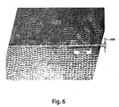
- FIG. 6 is a copy of a STEM (scanning transmission electron microscope) image that illustrates the presence of a silicon nitride strain-absorbing layer between the aluminum nitride layer and the silicon substrate.
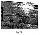
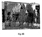
- FIGS. 7A-8B are copies of TEM images taken of vertical cross-sections of the same structure.
- the "*" indicates identical spatial positions on the images.
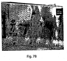
- FIGS. 8A and 8B are respective copies of FIGS. 7A and 7B with dislocations present in the gallium nitride material region and a first portion of the transition layer (Al 0.3 Ga 0.7 N) highlighted by dashed lines. It should be noted that the second portion of AlGaN transition layer and the AlN layer indicate similar dislocation densities, but dashed lines were not individually noted for the sake of clarity.
- FIGS. 7B and 8B there are a number of dislocations present in FIGS. 7B and 8B which are not present in FIGS. 7A and 8A . This is also indicative of these dislocations being edge dislocations or mixed dislocations.
- This example establishes formation of a III-nitride material layers/regions having a very low screw dislocation density. No screw dislocations were detected in the TEM images.
Abstract
Description
- The invention relates generally to III-nitride materials and, more particularly, to III-nitride (e.g., gallium nitride) material structures including low dislocation densities, as well as methods associated with the same.
- III-nitride materials include gallium nitride (GaN), aluminum nitride (AlN), indium nitride (InN) and their respective alloys (e.g., AlGaN, InGaN, AlInGaN and AlInN). In particular, gallium nitride materials (GaN and its alloys) have attractive properties including the ability to efficiently emit blue light, the ability to transmit signals at high frequency, and others. Accordingly, gallium nitride materials are being widely investigated in many microelectronic applications such as transistors, field emitters, and optoelectronic devices. Semiconductor structures that include gallium nitride material regions oftentimes include regions of other III-nitride materials (e.g., AlN). Such layers, for example, may function as buffer or intermediate layers positioned between a substrate and an overlying gallium nitride material region.
- III-nitride materials have different crystal structures and properties than many common substrates including silicon, silicon carbide and sapphire. Thus, when III-nitride materials are formed on such substrates, these differences may lead to the formation of defects including dislocations. For example, dislocations may result from differences between the lattice constants of the substrate and the III-nitride material; differences between the thermal expansion coefficients of the substrate and the III-nitride material; as well as, substrate quality including misorientation and defects.
- Dislocations are linear imperfections in a crystalline array of atoms. Types of dislocations include edge dislocations, screw dislocations and mixed dislocations (which have an edge component and a screw component). The presence of dislocations in III-nitride materials that are in the vicinity of the active region in a device can impair device performance. For example, the dislocations can function as scattering centers which effect electron transport and, thus, impair electrical performance. Also, the dislocations can function as non-radiative recombination centers which reduce performance of opto-electronic devices. Furthermore, dislocations can lead to inhomogeneities in composition and formation of macro-defects which can also negatively effect device performance.
- Certain conventional vertical growth processes (i.e., growth that proceeds in a vertical direction from the underlying layer) form III-nitride material regions having screw dislocation densities of greater than about 1012 /cm3. Lateral growth processes can produce localized areas within III-nitride material regions having low defect densities, while other areas within the regions have relatively high defect densities. Lateral growth processes are typically more complex than vertical growth processes.
-
JP 9134878 A -
US 2004 021147 A describes a GaN-based ultraviolet light emitting diode. An undoped GaN seed crystal is grown on a sapphire substrate by metalorganic vapor phase epitaxy (MOVPE). SiO2 is deposited and processed to form dielectric masks with a stripped pattern. To obtain a flat surface, undoped GaN is re-grown by epitaxial lateral overgrowth from starting points at portions of the seed crystal that are exposed through the dielectric masks. - The invention provides III-nitride materials having low dislocation (e.g., screw dislocation) densities including structures, devices and methods associated with the materials.
- In one embodiment, a semiconductor structure is provided. The structure comprises a substrate, a silicon nitride-based strain absorbing layer formed on the substrate, a III-nitride material region formed on the strain-absorbing layer, wherein a cross sectional area of the III-nitride material region greater than or equal to approximately 100 square microns and less than approximately 100 nm from a bottom surface of the III-nitride material region has a screw dislocation density of less than about 108/cm2 and an edge dislocation density of greater than about 108 /cm2 and a second III-nitride material region formed on the III-nitride material region, wherein a cross sectional area of the second III-nitride material region greater than or equal to approximately 100 square microns and less than approximately 100 nm from a bottom surface of the second III-nitride material region has a screw dislocation density of less than 108/cm2.
- In one example, a semiconductor structure is provided. The structure comprises a III-nitride material region including an area having dimensions of at least about 100 microns x 100 microns and a screw dislocation density of less than about 104/cm2.
- In another example, a semiconductor structure is provided. The structure comprises a semiconductor region having a top surface; and, a III-nitride material region formed over the top surface and having a different composition than the semiconductor region. A cross-sectional area of the III-nitride material region within 100 nanometers of the top surface has a screw dislocation density of less than about 108/cm2.
- In another example, a semiconductor structure is provided. The structure comprises a III-nitride material region having a screw dislocation density of less than about 108/cm2 and an edge dislocation density of greater than about 108/cm2.
- In another example, a semiconductor structure is provided. The structure comprises a III-nitride material region having an edge dislocation density and a screw dislocation density. The edge dislocation density is at least 100 times greater than the screw dislocation density.
- In another example, a semiconductor structure is provided. The structure comprises a substrate, and a silicon nitride-based material layer having a thickness of less than 100 Angstroms and substantially covering an entire top surface of the substrate. The structure further comprises a III-nitride material region formed over the silicon nitride-based material layer and having a screw dislocation density of less than about 108/cm2.
- In another embodiment, a method of forming a semiconductor structure is provided. The method comprises providing a substrate; forming a silicon nitride-based strain absorbing layer on the substrate; vertically growing a III-nitride material region on the strain-absorbing layer, wherein a cross sectional area of the III-nitride material region greater than or equal to approximately 100 square microns and less than approximately 100 nm from a bottom surface of the III-nitride material region has a screw dislocation density of less than about 108/cm2 and an edge dislocation density of greater than about 108/cm2; and, vertically growing a second III- nitride material region over the III-nitride material region, wherein a cross sectional area of the second III-nitride material region greater than or equal to approximately 100 square microns and less than approximately 100 nm from a bottom surface of the second III -nitride material region has a screw dislocation density of less than about 108/cm2.
- In another example, a method of forming a semiconductor structure is provided. The method comprises providing a semiconductor material region having a top surface; and, vertically growing a III-nitride material region over the semiconductor material region. The III-nitride material region has a composition different than the semiconductor material region. A screw dislocation density in a cross-sectional area of the III-nitride material region located within 100 nanometers of the top surface of the semiconductor material region is less than about 108/cm2.
- Other aspects, embodiments and features of the invention will become apparent from the following detailed description of the invention when considered in conjunction with the accompanying drawings. The accompanying figures are schematic and are not intended to be drawn to scale. In the figures, each identical, or substantially similar component that is illustrated in various figures is represented by a single numeral or notation. For purposes of clarity, not every component is labeled in every figure. Nor is every component of each embodiment of the invention shown where illustration is not necessary to allow those of ordinary skill in the art to understand the invention.
-
-
FIG. 1 illustrates a structure including III-nitride material regions having low screw dislocation densities according to one embodiment of the present invention. -
FIG. 2 illustrates a structure including III-nitride material regions having low screw dislocation densities according to another embodiment of the present invention. -
FIG. 3 illustrates a structure including III-nitride material regions having low screw dislocation densities according to another embodiment of the present invention. -
FIG. 4 illustrates a free-standing III-nitride material region having a low screw dislocation density according to another embodiment of the present invention. -
FIG. 5 illustrates a FET device including III-nitride material regions having low screw dislocation densities according to one embodiment of the invention. -
FIG. 6 is a copy of a STEM (scanning transmission electron microscope) image that illustrates the presence of a silicon nitride strain-absorbing layer between an aluminum nitride layer and a silicon substrate as described in Example 1. -
FIGS. 7A and7B are respective copies of bright field cross-sectional TEM images of a structure as described in Example 1. -
FIGS. 8A and8B are respective copies of the TEM images ofFIGS. 7A and7B with dislocations highlighted by dashed lines as described in Example 1. - The invention provides semiconductor structures including one or more III-nitride material region(s) (e.g., a gallium nitride material region) and methods associated with such structures. The III-nitride material region(s) advantageously have a low dislocation density and, in particular, a low screw dislocation density. In some embodiments, the presence of screw dislocations in the III-nitride material region(s) may be essentially eliminated. As described further below, the presence of a strain-absorbing layer underlying the III-nitride material region(s), amongst other factors, can contribute to achieving the low screw dislocation densities. In some embodiments, the III-nitride material region(s) having low dislocation densities include a gallium nitride material region which functions as the active region of the device. The low screw dislocation densities of the active device region (e.g., gallium nitride material region) can lead to improved properties (e.g., electrical and optical) by decreasing electron scattering, limiting non-radiative recombination, increasing compositional uniformity, and reducing macro-defect formation, amongst other effects.
-
FIG. 1 illustrates asemiconductor structure 10 according to one embodiment of the invention. The semiconductor structure includes a strain-absorbinglayer 12 formed on asubstrate 14. A series of III-nitride material regions are formed on the strain-absorbing layer. In this illustrative embodiment, the series of III-nitride material regions includes anintermediate layer 15, atransition layer 16 and a galliumnitride material region 18. As described further below, the strain-absorbing layer (amongst other factors) may help contribute to limiting generation of screw dislocation densities in at least one (and, in some cases, all) of the overlying III-nitride layers and, in particular, in the gallium nitride material region. Semiconductor structures of the invention may form the basis of a number of semiconductor devices including transistors (e.g., FET), Schottky diodes, light emitting diodes and laser diodes, amongst others. - When a layer is referred to as being "on" or "over" another layer or substrate, it can be directly on the layer or substrate, or an intervening layer also may be present. A layer that is "directly on" another layer or substrate means that no intervening layer is present. It should also be understood that when a layer is referred to as being "on" or "over" another layer or substrate, it may cover the entire layer or substrate, or a portion of the layer or substrate.
- As used herein, the term "III-nitride material" refers to any Group III element-nitride compound including boron nitride (BN), aluminum nitride (AlN), gallium nitride (GaN), indium nitride (InN) and thalium nitride (TIN), as well as any alloys including Group III elements and Group V elements (e.g., AlxGa(1-x)N, AlxInyCa(1-x-y)N, InyGa(1-y)N AlyIn(1-y)N, GaAsaPb N(1-a-b), AlxInyGa(1-x-y)ASaPbN(1-a-b) and the like). Typically, when present, arsenic and/or phosphorous are at low concentrations (i.e., less than 5 weight percent). III-nitride materials may be doped n-type or p-type, or may be intrinsic.
- As used herein, the phrase "gallium nitride material" refers to gallium nitride (GaN) and any of its alloys, such as aluminum gallium nitride (AlxGa(1-x)N), indium gallium nitride (InyGa(1-y)N), aluminum indium gallium nitride (AlxInyGa(1-x-y)N), gallium arsenide phosporide nitride (GaAsaPbN(1-a-b)), aluminum indium gallium arsenide phosporide nitride (AlxInyGa(1-x-y)AsaPbN(1-a-b)), amongst others. Typically, when present, arsenic and/or phosphorous are at low concentrations (i.e., less than 5 weight percent). In certain preferred embodiments, the gallium nitride material has a high concentration of gallium and includes little or no amounts of aluminum and/or indium. In high gallium concentration embodiments, the sum of (x + y) may be less than 0.4, less than 0.2, less than 0.1, or even less. In some cases, it is preferable for the gallium nitride material layer to have a composition of GaN (i.e., x + y = 0). Gallium nitride materials may be doped n-type or p-type, or may be intrinsic. Suitable gallium nitride materials have been described in commonly-owned
U.S. Patent No. 6,649,287 which is incorporated herein by reference. - As used herein, the term "region" may refer to one layer (e.g.,
layer 15, layer 16) or may refer to a series of layers (e.g., galliumnitride material region 18 includinglayers - At least one of the III-nitride material regions (e.g.,
intermediate layer 15,transition layer 16, gallium nitride material region 18) formed on the strain-absorbing layer has low screw dislocation densities. In some embodiments, it may be preferred for all of the III-nitride material regions formed on the strain-absorbing layer to have low screw dislocation densities (including the screw dislocation density values noted below). It may be particularly preferable for the gallium nitride material region to have a low screw dislocation density because in many device applications the active device region is formed in the gallium nitride material region, as described further below. - However, it should be understood, that in certain embodiments, it may be possible for one or more of these III-nitride material regions to have higher screw dislocation densities.
- In some embodiments, the screw dislocation density in one (or more) of the III-nitride material regions above the strain-absorbing layer is less than about 108 screw dislocations/cm2, and, in some cases, less than about 106/cm2. It is even possible to achieve significantly lower screw dislocation densities within the scope of the present invention. In some embodiments, one (or more) of the III-nitride material regions have very low screw dislocation densities of less than about 104/cm2 and, in some cases, less than about 102/cm2. In some embodiments, it is even possible for one (or more) of the III-nitride material regions to have substantially zero screw dislocations.
- As used herein, units for screw dislocation density may be expressed as "screw dislocations/cm2" or "/cm2".
- In some preferred embodiments, at least the gallium nitride material region has the low screw dislocation density values noted above.
- The specific screw dislocation density depends, in part, on the particular structure including factors such as the thickness, composition and crystal structure of the strain-absorbing layer; the composition, thickness and crystal structure of the overlying III-nitride material layer(s)/region(s); as well as, the composition, thickness, and crystal structure of the substrate, amongst other factors.
- Screw dislocation densities may be measured using known techniques. For example, a diffraction contrast technique (e.g., g-vector analysis), which involves comparing transmission electron microscope (TEM) images of the material structure obtained under different imaging conditions, may be used to selectively view the screw dislocations and measure the screw dislocation density.
- It should be understood that the screw dislocation densities described herein are measured over a representative area. The representative area may depend, in part, on the actual dislocation density being measured. For example, a representative area of about 100 microns squared (e.g., 10 micron x 10 micron) may be suitable for measuring screw dislocation densities on the order of 108/cm2. Larger representative areas may be used for smaller screw dislocation densities.
- Advantageously, in some embodiments, the above-identified screw dislocation density ranges are present throughout one (or more) of the respective III-nitride material region(s) overlying the stress-absorbing layer. That is, throughout the entire volume of at least one (or more) of the III-nitride material region(s), the screw dislocation densities ranges identified above may be achieved.
- It should be understood that, in some embodiments, all of the III-nitride material regions (e.g.,
intermediate layer 15, atransition layer 16 and a gallium nitride material region 18) formed over the strain-absorbing layer have the above-identified screw dislocation densities. - The low screw dislocation densities are also achievable across large areas of III-nitride material regions. For example, the above-identified screw dislocation densities may be found in regions having an area of greater than about 104 square microns; or, greater than about 1 mm2. In some cases, the areas of the III-nitride material regions having the low screw dislocation densities may be greater than about 1 cm2, or more.
- The above-noted areas may comprises a variety of dimensions (i.e., lengths, widths) including similar lengths and widths. For example, the above-identified screw dislocation densities may be found in areas having dimensions of greater than about 100 microns x 100 microns; or, greater than about 1 mm x I mm. In some cases, the areas of the III-nitride material regions having the low screw dislocation densities may have dimensions of greater than about 1 cm x 1 cm, or more.
- The consistently low screw dislocation densities across large areas and/or throughout the entire region(s) provides advantages over certain prior art techniques (e.g., certain lateral growth processes) that form, within a respective III-nitride material region, areas of low screw dislocation density and also areas of high screw dislocation density (e.g., greater than 108/cm2).
- In some embodiments, the III-nitride material region may have a substantially constant screw dislocation density throughout the entire region and/or area. In some embodiments, the screw dislocation density is substantially constant along an axial direction (i.e., z-axis in
FIG. 1 ) and is also substantially constant along a radial direction (i.e., x-axis inFIG. 1 ). - The above-identified screw dislocation densities are achievable within areas of the III-nitride material region proximate to (e.g., within 100 nanometers, or within 50 nanometers) an underlying semiconductor region (e.g., substrate or semiconductor layer) formed of a different material composition. The area, for example, is a cross-sectional area (e.g., A, in
FIG. 1 ) of the III-nitride material region within 100 nanometers (or, within 50 nanometers) of the upper surface of the underlying region. The cross-sectional area may extend across the III-nitride region and may be parallel to the lower surface of the III-nitride material region (or the upper surface of the underlying region). The cross-sectional area may have any of the area values described above. The cross-sectional area and the III-nitride material region may be directly above the underlying semiconductor region, as shown. - In these embodiments, strain-absorbing layer 12 (with a thickness of less than 100 nanometers) may be formed between the III-nitride material region and the underlying semiconductor region (e.g., substrate 14).
- In some cases, above-identified screw dislocation densities are achievable within an area of the III-nitride material region formed within 100 nanometers (or, 50 nanometers) of the top surface of a substrate having a different material composition than the III-nitride material region. In these cases, the substrate may be formed of silicon, silicon carbide, sapphire (or, other substrate materials described below that meet this condition). The III-nitride material region may be
intermediate layer 15,transition layer 16 or galliumnitride material region 18, depending on the structure. - In some cases, above-identified screw dislocation densities are achievable in a III-nitride material region formed within 100 nanometers (or, 50 nanometers) of the top surface of a semiconductor layer (i.e., non-substrate) having a different material composition than the III-nitride material region. For example, the semiconductor material layer may be formed of a III-nitride material having a different composition than the III-nitride material region.
- The mechanism for limiting/eliminating screw dislocations in structures of the present invention may not have as significant an effect on lowering the edge dislocation density or mixed dislocation density. For example, in some embodiments, the edge dislocation density and/or mixed dislocation density may be greater than about 108/cm2 in the III-nitride material region having the reduced screw dislocation density. In some cases, the edge dislocation density and/or mixed dislocation density is at least 100 times, or at least 104 times, greater than the screw dislocation density in the III-nitride material region. In embodiments having very low screw dislocation densities, the edge dislocation density and/or mixed dislocation density may be at least 106, or at least 108 times, the screw dislocation density in the III-nitride material region. In embodiments that do not have low edge and/or mixed dislocation densities, it should be understood that the structures still have the above-identified advantages associated with lower screw dislocation densities.
- It should be understood, however, that in some embodiments of the invention lower edge and mixed dislocation densities than those described above may be achieved. It also should be understood that the above-referenced edge dislocation densities may be present throughout the III-nitride material region(s) and, at least, in the same portions of the III-nitride material region(s) having reduced screw dislocation densities.
- It is believed that the low screw dislocation densities are achieved, at least in part, by the presence of the strain-absorbing layer. However, it should be understood that in certain embodiments of the invention that do not include the strain-absorbing layer, the III-nitride material regions may also have the low screw dislocation densities. Other factors include the composition, thickness and crystal structure of the intermediate layer, transition layer and III-nitride material region; the composition, thickness, and crystal structure of the substrate; and, process conditions described further below, amongst other factors.
- In particular, the composition, thickness and crystal structure of the strain-absorbing layer may contribute to reducing the formation of screw dislocations in the overlying III-nitride material layer(s)/region. The strain-absorbing layer may also reduce the formation of misfit dislocations in the layer formed on in the gallium nitride material region as described in commonly-owned, co-pending U.S. patent application publication number
US2005/0285141 A1, filed June 28, 2004 , entitled "Gallium Nitride Materials and Methods Associated with the Same" which is incorporated herein by reference. - Strain-absorbing
layer 12 helps absorb strain that arises due to lattice differences between the crystal structure of the substrate and the crystal structure of layer/region formed on the strain-absorbing layer (e.g.,intermediate layer 15 inFIG. 1 ;transition layer 16 inFIG. 2 ; and gallium nitride material region inFIG. 3 ). In the absence of the strain-absorbing layer, this strain is typically accommodated by the generation of misfit dislocations in the intermediate layer (or, other overlying layer) at the interface with the substrate. Thus, by providing an alternative mechanism for accommodating stress, the presence of the strain-absorbing layer may reduce the generation of misfit dislocations at the interface with the substrate. It is believed that the reduction in misfit dislocations can also lead to a reduction in screw dislocations in the overlying layers (e.g.,intermediate layer 15,transition layer 16 and gallium nitride material region 18). - Furthermore, the strain-absorbing layer can help absorb strain that arises due to differences in the thermal expansion rate of the substrate as compared to the thermal expansion rate of the intermediate layer and/or the gallium nitride material region. Such differences can lead to formation of misfit dislocations at the intermediate layer/substrate interface, or cracking in either the intermediate layer and/or gallium nitride material region. As described further below,
transition layer 16 also helps absorb this thermally-induced strain. - Suitable strain-absorbing layers have been described in commonly-owned, co-pending U.S. patent application publication number
US2005/0285141 A1, filed June 28, 2004 , entitled "Gallium Nitride Materials and Methods Associated with the Same" which is incorporated by reference above. In certain preferred embodiments, strain-absorbinglayer 12 is formed of a silicon nitride-based material. Silicon nitride-based materials include any silicon nitride-based compound (e.g., SixNy, such as SiN and Si3N4, SiCN, amongst others) including non-stoichiometric silicon nitride-based compounds. In some embodiments, a SiN strain-absorbing layer may be preferred. Silicon nitride material-based strain-absorbing layers may be particularly preferred when formed directly on a silicon substrate, as described further below. - It should also be understood that it is possible for the strain-absorbing layer to be formed of other types of materials according to other embodiments of the invention. Though all of the advantages associated with silicon nitride-based materials may not be achieved in these embodiments.
- In some embodiments, it is preferable for the strain-absorbing layer to have an amorphous (i.e., non-crystalline) crystal structure. Amorphous strain-absorbing layers are particularly effective in accommodating strain and, thus, reducing the generation of misfit dislocations.
- However, it should be understood that in certain embodiments of the invention, the strain-absorbing layer may have a single crystal or poly-crystalline structure. In these cases, however, all of the advantages associated with an amorphous strain-absorbing layer may not be realized.
- In some embodiments, it is preferred for the strain-absorbing layer to be very thin, particularly when formed of amorphous and/or silicon nitride-based materials. It has been discovered that very thin strain-absorbing layers (e.g., silicon nitride-based strain-absorbing layers) may enable formation of intermediate layer(s) having an epitaxial relationship with the substrate, while also being effective in reducing the number of misfit dislocations (which may lead to the reduced screw dislocations in the III-nitride material region(s)). In certain cases (e.g., when the strain-absorbing layer is amorphous), it is desirable for the strain-absorbing layer to have a thickness that is large enough to accommodate sufficient strain associated with lattice and thermal expansion differences between the substrate and
intermediate layer 15 to reduce generation of misfit dislocations. In these cases, it may also be desirable for the strain-absorbing layer to be thin enough so that the intermediate layer has an epitaxial relationship with the substrate. This can be advantageous for formation of a high quality, single crystal III-nitride material region (e.g., gallium nitride material region). If the strain-absorbing layer is too thick, then the intermediate layer is not formed with epitaxial relationship with the substrate. - In some embodiments, the strain-absorbing layer has a thickness of less than about 100 Angstroms which, in these embodiments, can allow the epitaxial relationship between the substrate and the intermediate layer. In some embodiments, it may be preferable for the strain-absorbing layer to have a thickness of less than about 50 Angstroms to allow for the epitaxial relationship.
- The strain-absorbing layer may have a thickness of greater than about 10 Angstroms which, in these embodiments, is sufficient to accommodate strain (e.g., resulting from lattice and thermal expansion differences) and can facilitate forming a strain-absorbing layer that covers the entire substrate, as described further below. In other embodiments, the strain-absorbing layer may have a thickness of greater than about 20 Angstroms to sufficiently accommodate strain.
- Suitable thickness ranges for the strain-absorbing layer include all of those defined by the ranges described above (e.g., greater than about 10 Angstroms and less than about 100 Angstroms, greater than about 10 Angstroms and less than about 50 Angstroms, and the like). Also, the strain-absorbing layer thickness may be between about 20 Angstroms and about 70 Angstroms.
- It should be understood that suitable thicknesses of the strain-absorbing layer may depend on a number of factors including the composition and crystal structure of the strain-absorbing layer; the composition, thickness and crystal structure of the intermediate layer; as well as the composition, thickness, and crystal structure of the substrate, amongst other factors. Suitable thicknesses may be determined by measuring the effect of thickness on misfit dislocation density and other factors (e.g., the ability to deposit an intermediate layer having an epitaxial relationship with the substrate, etc.). It is also possible for the strain-absorbing layer to have a thickness outside the above ranges.
- In some cases, the thickness of the strain-absorbing layer is relatively uniform across the entire layer. For example, in these cases, the strain-absorbing layer may have a thickness uniformity variation of less than 25 percent, or less than 10 percent, across the entire strain-absorbing layer.
- As described further below, in some embodiments, the strain-absorbing layer may be formed by nitridating a top surface region of a silicon substrate. That is, the surface region of the substrate may be converted from silicon to a silicon nitride-based material to form the strain-absorbing layer. It should be understood that, as used herein, such strain-absorbing layers may be referred to as being "formed on the substrate", "formed over the substrate", "formed directly on the substrate" and as "covering the substrate". Such phrases also refer to strain-absorbing layers that are formed by depositing a separate layer (e.g., using a separate nitrogen source and silicon source) on the top surface of the substrate and are not formed by converting a surface region of the substrate.
- In the illustrative embodiment, the strain-absorbing layer covers substantially the entire top surface of the substrate. This arrangement may be preferable to minimize the number of misfit dislocations in the intermediate layer and, thus, the number of screw dislocations in the III-nitride material region(s). In other embodiments, the strain-absorbing layer may cover a majority of the top surface of the substrate (e.g., greater than 50 percent or greater than 75 percent of the top surface area).
- Also, in the illustrative embodiment, strain-absorbing
layer 12 is formed across the entire area between the substrate and the intermediate layer. That is, the strain-absorbing layer separates the substrate and the intermediate layer at all points with the strain-absorbing layer being directly on the substrate and the intermediate layer being directly on the strain-absorbing layer. This arrangement may be preferable to minimize the number of misfit dislocations in the intermediate layer. In other embodiments, the strain-absorbing layer may be formed across a majority of the area (e.g., greater than 50 percent, or greater than 75 percent) between the substrate and the intermediate layer. If the strain-absorbing layer is not present across the entire (or, at least, the majority of the) area between the substrate and the intermediate layer, the above-noted advantages associated with the strain-absorbing layer may not be realized. - The extent that the strain-absorbing layer covers the substrate (and the area between the intermediate layer and the substrate) in the present invention may be distinguished from certain prior art techniques in which a discontinuous silicon nitride layer is formed (in some cases, inadvertently) between a silicon substrate and an overlying layer.
- It should be understood that, in other embodiments, the strain-absorbing layer may be positioned in other locations such as between two different layers (i.e., not formed directly on the substrate). In these embodiments, the strain-absorbing layer may reduce the formation of misfit dislocations and reduce the propagation of screw dislocations to the layer(s)/region(s) that overlie the strain-absorbing layer. The strain-absorbing layer may cover the layer on which it is formed to a similar extent as described above in connection with the strain-absorbing layer covering the substrate.
- As noted above, the presence of the strain-absorbing layer advantageously results in very low misfit dislocation densities within the intermediate layer (e.g., at, or very near, an interface between the strain-absorbing layer and the intermediate layer). In some embodiments of the invention, the misfit dislocation density in the overlying layer is less than about 1010/cm2; and, in other embodiments, less than about 108/cm2. Even lower misfit dislocation densities in the overlying layer may be achieved, for example, less than about 105/cm2. In some cases, the presence of misfit dislocations may not be readily detectable which generally means that the misfit dislocation density is less than about 102/cm2. The specific misfit dislocation density depends, in part, on the particular structure including factors such as the thickness, composition and crystal structure of the strain-absorbing layer; the composition, thickness and crystal structure of the overlying layer; as well as the composition, thickness, and crystal structure of the substrate, amongst other factors.
- It may be preferred for
structure 10 to include anintermediate layer 15 formed of a nitride-based material. Suitable nitride-based materials include, but are not limited to, aluminum nitride-based materials (e.g., aluminum nitride, aluminum nitride alloys) and gallium nitride materials. In some cases, the intermediate layer has a constant composition. In other cases, as described further below, the intermediate layer may be compositionally-graded. Suitable compositionally-graded layers are described further below and have been described in commonly-ownedU.S. Patent No. 6,649,287 , entitled "Gallium Nitride Materials and Methods" filed on December 14, 2000, which is incorporated herein by reference. - It may be preferable for the intermediate layer to have a single crystal structure. As noted above, in some embodiments, the thickness of the strain-absorbing layer is controlled so that the intermediate layer has an epitaxial relationship with the substrate. It may be advantageous for the intermediate layer to have a single crystal structure because it facilitates formation of a single crystal, high quality gallium nitride material region having low screw dislocation densities. In some embodiments, the intermediate layer has a different crystal structure than the substrate.
- It should also be understood that the intermediate layer may not have a single crystal structure and may be amorphous or polycrystalline, though all of the advantages associated with the single crystal intermediate layers may not be achieved.
- The intermediate layer may have any suitable thickness. For example, the intermediate layer may be between about 10 nanometers and 5 microns, though other thicknesses are also possible.
- It should be understood that certain embodiments of the invention may not include an intermediate layer 15 (e.g., as shown in
Fig. 2 ). - In the illustrative embodiment,
transition layer 16 is formed directly on the intermediate layer. In certain embodiments, such as when the intermediate layer has a constant composition, it may be preferred for the transition layer to be formed of a compositionally-graded material (e.g., a compositionally-graded nitride-based material). Suitable compositionally-graded layers have been described in commonly-ownedU.S. Patent No. 6,649,287 which is incorporated by reference above. - Compositionally-graded transition layers have a composition that is varied across at least a portion of the layer. Compositionally-graded transition layers are particularly effective in reducing crack formation in gallium nitride material regions formed on the transition layer by lowering thermal stresses that result from differences in thermal expansion rates between the gallium nitride material and the substrate (e.g., silicon). Compositionally-graded transition layers may also contribute to reducing generation of screw dislocations in the III-nitride material layer(s)/region(s) (e.g., gallium nitride material region). In some cases, the compositionally-graded transition layers may also contribute to reducing mixed and edge dislocation densities.
- According to one set of embodiments, the transition layer is compositionally-graded and formed of an alloy of gallium nitride such as AlxInyGa(1-x-y)N, AlxGa(1-x)N, and InyGa(1-y)N. In these embodiments, the concentration of at least one of the elements (e.g., Ga, Al, In) of the alloy is varied across at least a portion of the thickness of the transition layer. When
transition layer 16 has an AlxInyGa(1-x-y)N composition, x and/or y may be varied. When the transition layer has a AlxGa(1-x)N composition, x may be varied. When the transition layer has a InyGa(1-y)N composition, y may be varied. - In certain preferred embodiments, it is desirable for the transition layer to have a low gallium concentration at a back surface which is graded to a high gallium concentration at a front surface. It has been found that such transition layers are particularly effective in relieving internal stresses within gallium
nitride material region 18. For example, the transition layer may have a composition of AlxGa(1-x)N, where x is decreased from the back surface to the front surface of the transition layer (e.g., x is decreased from a value of 1 at the back surface of the transition layer to a value of 0 at the front surface of the transition layer). - In some preferred embodiments,
structure 10 includes an aluminum nitrideintermediate layer 15 and a compositionally-gradedtransition layer 16. In some preferred embodiments, the compositionally-graded transition layer has a composition of AlxGa(1-x)N, where x is graded from a value of 1 at the back surface of the transition layer to a value of 0 at the front surface of the transition layer. The composition, for example, can be graded discontinuously (e.g., step-wise) or continuously. One discontinuous grade may include steps of AlN, Al0.6Ga0.4N and Al0.3Ga0.7N proceeding in a direction toward the gallium nitride material region. - It should be understood that, in other cases,
transition layer 16 may have a constant composition and may not be compositionally-graded. In some cases (e.g., when the substrate is not a silicon substrate), the transition layer may have a constant composition. Suitable compositions include, but are not limited to, aluminum nitride-based materials (e.g., aluminum nitride, aluminum nitride alloys) and gallium nitride materials. In these constant composition embodiments, the transition layer may be similar to the intermediate layer in other illustrative embodiments. - The strain absorbing layer, intermediate layer and transition layer are not typically (though may be) part of the active region of devices formed from structures of the invention. As described above, these layers may be formed to facilitate deposition of gallium
nitride material region 18. However, in some cases, the intermediate layer and/or transition layer may have other functions including functioning as a heat spreading layer that helps remove heat from active regions of the semiconductor structure during operation of a device. For example, such transition layers that function as heat spreading layers have been described in commonly-owned, co-pending U.S. Patent Application Publication NumberUS2002/0117695 A1 entitled "Gallium Nitride Materials Including Thermally-Conductive Regions," filed February 23, 2001, which is incorporated herein by reference. Active regions of devices formed from the structure of the invention may be formed in galliumnitride material region 18. Galliumnitride material region 18 comprises at least one gallium nitride material layer. In some cases, galliumnitride material region 18 includes only one gallium nitride material layer. In other cases, galliumnitride material region 18 includes more than one gallium nitride material layer. For example, the gallium nitride material region may include multiple layers (e.g., 18a, 18b, 18c) as shown inFIG. 5 . In embodiments having more than one gallium nitride material layer, each layer may have the reduced screw dislocation densities noted above. - Suitable gallium nitride material layer arrangements have been described, for example, in commonly-owned, co-pending U.S. Patent Application Publication Number
US2005/0133818 A1 entitled "Gallium Nitride Material Devices Including an Electrode-Defining Layer and Methods of Forming the Same," filed December 17, 2003, which is incorporated herein by reference. - Preferably, gallium
nitride material region 18 also has a low crack level in addition to the low screw dislocation densities noted above. As described above, the transition layer (particularly when compositionally-graded) and/or intermediate layer may reduce crack formation. Gallium nitride materials having low crack levels have been described inU.S. Patent No. 6,649,287 incorporated by reference above. In some cases, the gallium nitride material region has a crack level of less than 0.005 µm/µm2. In some cases, the gallium nitride material region has a very low crack level of less than 0.001 µm/µm2. In certain cases, it may be preferable for the gallium nitride material region to be substantially crack-free as defined by a crack level of less than 0.0001 µm/µm2. - In certain cases, gallium
nitride material region 18 includes a layer (or layers) which have a single crystal (i.e., monocrystalline) structure. In some cases, the gallium nitride material region includes one or more layers having a Wurtzite (hexagonal) structure. - The thickness of gallium
nitride material region 18 and the number of different layers are dictated, at least in part, on the application in which the structure is used. At a minimum, the thickness of the gallium nitride material region is sufficient to permit formation of the desired structure or device. The gallium nitride material region generally has a thickness of greater than 0.1 micron, though not always. In other cases, galliumnitride material region 18 has a thickness of greater than 0.5 micron, greater than 2.0 microns, or even greater than 5.0 microns. In some cases, gallium nitride material region has a thickness of less than 10.0 microns, or less than 5.0 microns. It may be advantageous for the gallium nitride material region to have thicknesses less than these values to limit processing times and for other processing reasons. - In some embodiments, the III-nitride material layer(s)/region(s) (e.g., gallium nitride material regions) may comprise limited amounts, or be substantially free, of additives (other than dopants). For example, the gallium nitride material may include less than about 0.01 ppm of alkali metal elements, or may be substantially free of alkali metal elements. This is an advantage over certain prior art processes, which may have used alkali metals in III-nitride material production, due to the elimination of impurities.
- As shown, the layers/regions of the device (e.g., strain-absorbing layer, intermediate layer, transition layer, gallium nitride material region) may be substantially planar in the final device or structure. As described further below, substantially planar layers/regions may be grown in vertical (e.g., non-lateral) growth processes. Certain lateral growth processes may lead to structures having non-planar layers/regions (e.g., as shown in
U.S. Patent No. 6,265,289 ). Planar layers/regions (and substrates, as noted below) can be advantageous in some embodiments, for example, in forming gallium nitride material regions having substantially constant screw dislocation densities and in simplifying processing, amongst other advantages. Though it should be understood that, in some embodiments of the invention, lateral growth processes may be used (in some cases, combined with vertical growth processes) as described further below. - The layers/regions may form a substantially planar interface with respective underlying layers/regions (including substrate). For example, the gallium nitride material region may form a substantially planar interface with
transition layer 16; and, strain-absorbinglayer 12 or thetransition layer 16 may form a substantially planar interface with the substrate. This also may be indicative of a vertical growth process, in contrast with structures formed in lateral growth processes (e.g., as shown inU.S. Patent No. 6,265,289 ). Forming a substantially planar interface between the gallium nitride material region and the underlying layer (e.g., transition layer 16) may lead to several advantages including promoting formation of substantially constant screw dislocation densities in the gallium nitride material region and simplifying processing, amongst other advantages. - It should be understood that the structures of the present invention are not limited to substantially planar layers/regions and/or interfaces. In some embodiments, the structures include non-planar layers/regions and/or interfaces.
- In some embodiments, the layers/regions may form a continuous interface with respective underlying layers/regions (including substrate). That is, the layers/regions of the structure (e.g., strain-absorbing layer, intermediate layer, transition layer, gallium nitride material region) may continuously extend across respective underlying layers/regions. For example, the gallium nitride material region may form a continuous interface with
transition layer 16; and, strain-absorbinglayer 12 or thetransition layer 16 may form a continuous interface with the substrate. The layers/regions may also continuously cover the top surface of the respective underlying layers/regions. - As described above, in certain preferred embodiments,
substrate 14 is a silicon substrate. As used herein, a silicon substrate refers to any substrate that includes a silicon surface. Examples of suitable silicon substrates include substrates that are composed entirely of silicon (e.g., bulk silicon wafers), silicon-on-insulator (SOI) substrates, silicon-on-sapphire substrate (SOS), and SIMOX substrates, amongst others. Suitable silicon substrates also include substrates that have a silicon wafer bonded to another material such as diamond, AlN, or other polycrystalline materials. Silicon substrates having different crystallographic orientations may be used, though single crystal silicon substrates are preferred. In some cases, silicon (111) substrates are preferred. In other cases, silicon (100) substrates are preferred. - It should be understood that other types of substrates may also be used including sapphire, silicon carbide, indium phosphide, silicon germanium, gallium arsenide, gallium nitride, aluminum nitride and other III-V compound substrates. However, in embodiments that do not use silicon substrates, all of the advantages associated with silicon substrates may not be achieved. In some embodiments, it may be preferable to use non-nitride material-based substrates such as silicon, sapphire, silicon carbide, indium phosphide, silicon germanium and gallium arsenide.
- In some cases (e.g.,
FIG. 4 ), as described further below, the substrate (and other layers) may be removed to form a free-standing III-nitride material region having low screw dislocation densities. -
Substrate 14 may have any suitable dimensions. Suitable diameters may include, but are not limited to, about 2 inches (50 mm), 4 inches (100 mm), 6 inches (150 mm), and 8 inches (200 mm). Advantageously, the strain-absorbing layer may be used to form a high quality gallium nitride material region on substrates (e.g., silicon substrates) over a variety of thicknesses. In some cases, it may be preferable for the substrate to be relatively thick, such as greater than about 125 micron (e.g., between about 125 micron and about 800 micron, or between about 400 micron and 800 micron). Relatively thick substrates may be easy to obtain, process and can resist bending which can occur, in some cases, in thinner substrates. In other embodiments, thinner substrates (e.g., less than 125 microns) are used, though these embodiments may not have the advantages associated with thicker substrates, but can have other advantages including facilitating processing and/or reducing the number of processing steps. In some processes, the substrate initially is relatively thick (e.g., between about 200 microns and 800 microns) and then is thinned during a later processing step (e.g., to less than 150 microns). - In some preferred embodiments, the substrate is substantially planar in the final device or structure. Substantially planar substrates may be distinguished from substrates that are textured and/or have trenches formed therein (e.g., as in
U.S. Patent No. 6,265,289 ). Substantially planar substrates may facilitate formation of substantially planar layers/regions thereupon. -
FIG. 2 illustrates asemiconductor structure 20 according to another embodiment of the invention.Semiconductor structure 20 is similar to that shown inFIG. 1 except the structure does not includeintermediate layer 15. -
FIG. 3 illustrates asemiconductor structure 22 according to another embodiment of the invention.Semiconductor structure 22 is similar to that shown inFIG. 1 except the structure does not includeintermediate layer 15 ortransition layer 16. -
FIG. 4 illustrates astructure 40 that comprises a free-standing galliumnitride material region 18. The free-standing gallium nitride material region may be formed by removing the substrate and layers (e.g., 12, 15, 16) underlying the gallium nitride material region. For example, the substrate and layers maybe removed by etching processes. In this embodiment, the gallium nitride material region may have any of the characteristics described above including the low screw dislocation densities. In particular, it may be advantageous for the free-standing gallium nitride material region to have a substantially constant low screw dislocation density.Structure 40 may be further processed, for example, to form semiconductor devices. - Though
FIG. 4 shows a galliumnitride material region 18, it should be understood that any of the other III-nitride materials described herein may also be converted to a free-standing structure. - The semiconductor structures illustrated in
FIGS. 1-4 may form the basis of a variety of semiconductor devices. Suitable devices include, but are not limited to, transistors (e.g., FETs), as well as light-emitting devices including LEDs and laser diodes. The devices have active regions that are typically, at least in part, formed within the gallium nitride material region. Also, the devices include a variety of other functional layers and/or features (e.g., electrodes). - For example,
FIG. 5 illustrates aFET device 30 according to one embodiment of the invention.Device 30 includes a source electrode 34, adrain electrode 36 and agate electrode 38 formed on gallium nitride material region 18 (which includes afirst layer 18b and asecond layer 18a). The device also includes anelectrode defining layer 40 which, as shown, is a passivating layer that protects and passivates the surface of the gallium nitride material region. A via 42 is formed within the electrode defining layer in which the gate electrode is, in part, formed. Strain-absorbinglayer 12 is formed directly on the substrate andintermediate layer 15 is formed directly on the strain-absorbing layer. In some embodiments, the intermediate layer is compositionally-graded. In some embodiments, the intermediate layer may have a constant composition (e.g., aluminum nitride or an aluminum nitride alloy) and a compositionally-graded transition layer is formed on the strain-absorbing layer. As shown, the gallium nitride material region includes multiple gallium nitride material layers (18a, 18b, 18c) with each layer having a low screw dislocation density. - In certain embodiments, it may be preferable for the gallium nitride material of
layer 18b to have an aluminum concentration that is greater than the aluminum concentration of the gallium nitride material oflayer 18a. For example, the value of x in the gallium nitride material oflayer 18b (with reference to any of the gallium nitride materials described above) may have a value that is between 0.05 and 1.0 greater than the value of x in the gallium nitride material oflayer 18a; or, between 0.05 and 0.5 greater than the value of x in the gallium nitride material oflayer 18a. For example,layer 18b may be formed of Al0.26Ga0.74N, whilelayer 18a is formed of GaN. This difference in aluminum concentration may lead to formation of a highly conductive region at the interface of thelayers layer 18c may be formed of GaN. - It should be understood that other structures and devices may be within the scope of the present invention including structures and devices that are not specifically described herein. Other structures may include other layers and/or features, amongst other differences.
-
Semiconductor structure 10 may be manufactured using known semiconductor processing techniques. In embodiments in which the strain-absorbing layer is a silicon nitride-based material (e.g., amorphous SiN), the strain-absorbing layer may be formed by nitridating a top surface of the silicon substrate as noted above. In a nitridation process, nitrogen reacts with a top surface region of the silicon substrate to form a silicon nitride-based layer. The top surface may be nitridated by exposing the silicon substrate to a gaseous source of nitrogen at elevated temperatures. For example, ammonia may be introduced into a reaction chamber in which a silicon substrate is positioned. The temperature in the reaction chamber may be between about 1000 °C and about 1100 °C and the pressure may be between about 20 torr and about 40 torr (in some cases, about 30 torr). The reaction between nitrogen and the silicon substrate is allowed to proceed for a reaction time selected to produce a layer having a desired thickness. - It should be understood that other processes may be used to form silicon nitride-based strain-absorbing layers including processes (e.g., CVD processes) that use separate nitrogen and silicon sources. Also, when the strain-absorbing layer is formed of another type of material (non-silicon nitride-based material), other deposition processes known in the art are used.
- In some embodiments, the strain-absorbing layer may be formed in-situ with the intermediate layer (and, in some cases, subsequent layers) of the structure. That is, the strain-absorbing layer may be formed during the same deposition step as the intermediate layer (and, in some cases, subsequent layers). In processes that grow a silicon nitride-based material strain-absorbing layer by introducing a nitrogen source (e.g., ammonia) into a reaction chamber as described above, a second source gas may be introduced into the chamber after a selected time delay after the nitrogen source. The second source reacts with the nitrogen source to form the intermediate layer, thus, ending growth of the strain-absorbing layer. For example, when the intermediate layer is formed of aluminum nitride, an aluminum source (e.g., trimethylaluminum) is introduced into the chamber at a selected time after the nitrogen source (e.g., ammonia). The time delay is selected so that the strain-absorbing layer grows to a desired thickness. The reaction between the second source (e.g., aluminum source) and the nitrogen source is allowed to proceed for a sufficient time to produce the intermediate layer. When the intermediate layer has a single crystal structure, the reaction conditions are selected appropriately. For example, the reaction temperature may be greater than 700 °C, such as between about 1000 °C and about 1100 °C. In some cases, lower growth temperatures may be used including temperatures between about 500 °C and about 600 °C.
- It should also be understood that the strain-absorbing layer may be formed in a separate process than the intermediate layer and subsequent layers. For example, the strain-absorbing layer may be formed on the substrate in a first process. Then, at a later time, the intermediate layers may be formed on the strain-absorbing layer in a second process.
- In the processes described above, the intermediate layer is grown in a vertical growth process. That is, the intermediate layer is grown in a vertical direction (i.e., along y-axis in
FIG. 1 ) with respect to the strain-absorbing layer. The ability to vertically grow the strain-absorbing layer having low misfit dislocation densities (which can contribute to the low screw dislocation densities) may be advantageous as compared to lateral growth processes which may be more complicated. -
Transition layer 16 and galliumnitride material region 18 may also be grown in the same deposition step as the intermediate layer and the strain-absorbing layer. In such processes, suitable sources are introduced into the reaction chamber at appropriate times. - According to one preferred method, the transition layer and gallium nitride material region (and intermediate layers, if present) are grown using a metalorganic chemical vapor deposition (MOCVD) process. It should be understood that other suitable techniques known in the art may also be utilized to deposit the transition layer and the gallium nitride material region including molecular beam epitaxy (MBE), hydride vapor phase epitaxy (HVPE), and the like.
- Generally, the MOCVD process involves introducing different source gases into an environment (e.g., a process system) and providing conditions which promote a reaction between the gases to form a layer. The reaction proceeds until a layer of desired thickness is achieved. The composition of the layer may be controlled, as described further below, by several factors including gas composition, gas concentration, and the reaction conditions (e.g., temperature and pressure).
- Examples of suitable source gases for MOCVD growth of the transition layer and gallium nitride material region, include trimethylaluminum (TMA) or triethylaluminum (TEA) as sources of aluminum; trimethylindium (TMI) or triethylindium (TEI) as sources of indium; trimethylgallium (TMG) or trimethylgallium (TEG) as sources of gallium; and ammonia (NH3) as a source of nitrogen. The particular source gas used depends upon the desired composition of the layers. For example, an aluminum source (e.g., TMA or TEA), a gallium source (TMG or TEG), and a nitrogen source are used to deposit films having an AlxGa1-xN composition.
- The flow rates of the source gases, the ratios of the source gases, and the absolute concentrations of the source gases may be controlled to provide transition layers and gallium nitride material regions having the desired composition. For the growth of AlxGa1-xN layers, typical TMA flow rates are between about 5 µmol/min and about 50 µmol/min with a flow rate of about 20 µmol/min being preferred in some cases; typical TMG flow rates are between about 5 µmol/min and 250 µmol/min, with a flow rate of 115µmol/min being preferred in some cases; and the flow rate of ammonia is typically between about 3 slpm to about 10 slpm. The reaction temperatures are generally between about 900°C and about 1200°C and the process pressures are between about 1 Torr and about 760 Torr. It is to be understood that the process conditions, and in particular the flow rate, are highly dependent on the process system configuration. Typically, smaller throughput systems require less flow than larger throughput systems.
- When forming a compositionally-graded transition layer, process parameters may be suitably adjusted to control the compositional grading. The composition may be graded by changing the process conditions to favor the growth of particular compositions. For example, to increase incorporation of gallium in the transition layer thereby increasing the gallium concentration, the flow rate and/or the concentration of the gallium source (e.g., TMG or TEG) may be increased. Similarly, to increase incorporation of aluminum into the transition layer thereby increasing the aluminum concentration, the flow rate and/or the concentration of the aluminum source (e.g., TMA or TEA) may be increased. The manner in which the flow rate and/or the concentration of the source is increased (or decreased) controls the manner in which the composition is graded. In other embodiments, the temperature and/or pressure is adjusted to favor the growth of a particular compound. Growth temperatures and pressures favoring the incorporation of gallium into the transition layer differ from the growth temperatures and pressures favoring the incorporation of aluminum into the transition layer. Thus, the composition may be graded by suitably adjusting temperature and pressure.
- When depositing a transition layer or a gallium nitride material region (or an intermediate layer) having a constant composition, however, the process parameters are maintained constant so as to provide a layer having a constant composition. When gallium nitride material regions include more than one gallium nitride material layer having different respective compositions, the process parameters may be changed at the appropriate time to change the composition of the layer being formed.
- It should be understood that all of the layers/regions on the substrate may be grown in the same process (i.e., the strain-absorbing layer, intermediate layer, transition layer and the gallium nitride material region). Or, respective layers/regions may be grown separately.
- The processes described involve growing the layers/regions (i.e., the strain-absorbing layer, intermediate layer, transition layer and the gallium nitride material region) in vertical growth processes. That is, these layers/regions are grown in a vertical direction with respect to underlying layers/regions (including substrate). The ability to vertically grow the layers/regions including the gallium nitride material region having low screw dislocation densities may be advantageous as compared to lateral growth processes which may be more complicated.
- However, in other embodiments of the invention (not shown), it is possible to grow, at least a portion of, gallium
nitride material region 18 using a lateral epitaxial overgrowth (LEO) technique that involves growing an underlying gallium nitride layer through mask openings and then laterally over the mask to form the gallium nitride material region, for example, as described inU.S. Patent No. 6,051;849 . - In other embodiments of the invention (not shown), it is possible to grow the gallium
nitride material region 18 using a pendeoepitaxial technique that involves growing sidewalls of gallium nitride material posts into trenches until growth from adjacent sidewalls coalesces to form a gallium nitride material region, for example, as described inU.S. Patent No. 6,265,289 . In these embodiments, for example, strain-absorbing layer 12 (and, in some cases, layers 15, 16) may be deposited on the sidewalls prior to lateral growth which may reduce screw dislocation densities in laterally-grown III-nitride material layers/regions (e.g., gallium nitride material regions). - Commonly-owned, co-pending U.S. Patent Application Publication Number
US2005/0133818 A1 entitled "Gallium Nitride Material Devices Including an Electrode-Defining Layer and Methods of Forming the Same," filed December 17, 2003, which is incorporated herein by reference, further describes techniques used to grow other layers and features shown in the embodiment ofFIG. 5 . - It should also be understood that other processes may be used to form structures and devices of the present invention as known to those of ordinary skill in the art.
- The following example is meant to be illustrative and is not limiting.
- This example illustrates the formation of a structure including III-nitride material layers/regions having low screw dislocation densities according to one embodiment of the present invention.
- A 100 mm silicon substrate was placed in a reaction chamber. Ammonia gas was introduced into the chamber as a nitrogen source. The temperature was maintained at 1030 °C and the pressure at about 30 torr. A strain-absorbing layer of amorphous silicon nitride (SiN) was formed.
- About 6 seconds after the introduction of ammonia, TMA was introduced into the chamber as an aluminum source. The temperature and pressure were respectively maintained at 1030 °C and about 30 torr. Growth proceeded for about 60 minutes. An aluminum nitride (AlN) was formed.
- After about 60 minutes, TMG was introduced into the chamber. Growth proceeded for about 40 minutes. An aluminum gallium nitride layer (Al0.6Ga0.4N) was formed.
- After about 40 minutes, the concentration of TMG being introduced into the chamber was increased and the concentration of TMA being introduced into the chamber was decreased. Growth proceeded for 20 minutes. An aluminum gallium nitride layer (Al0.3Ga0.7N) was formed.
- After about 20 minutes, the supply of TMA was turned off and only TMG was introduced into the chamber. A gallium nitride (GaN) layer was formed. Growth proceeded for 30 minutes
- The supply of TMA was turned back on and TMA and TMG were introduced into the chamber to grow a thin aluminum gallium nitride layer.
-
FIG. 6 is a copy of a STEM (scanning transmission electron microscope) image that illustrates the presence of a silicon nitride strain-absorbing layer between the aluminum nitride layer and the silicon substrate. - A g-vector analysis was used to assess screw dislocation density of overlying III-nitride material layers/regions using conventional TEM techniques.
FIGS. 7A-8B are copies of TEM images taken of vertical cross-sections of the same structure. For reference, the "*" indicates identical spatial positions on the images. -
FIG. 7A is an image with the g-vector (g = (00001)) perpendicular to the substrate surface.FIG. 7B is an image with the g-vector (g = ((1-100)) parallel to the substrate surface. -
FIGS. 8A and8B are respective copies ofFIGS. 7A and7B with dislocations present in the gallium nitride material region and a first portion of the transition layer (Al0.3Ga0.7N) highlighted by dashed lines. It should be noted that the second portion of AlGaN transition layer and the AlN layer indicate similar dislocation densities, but dashed lines were not individually noted for the sake of clarity. - As shown, all of the dislocations present in
FIGS. 7A and8A are also found inFIGS. 7B and8B . This one-to-one correspondence indicates that all of these dislocations are edge dislocations or mixed dislocations (which include an edge component). Thus, no screw dislocations were observed in the TEM images. - Also, there are a number of dislocations present in
FIGS. 7B and8B which are not present inFIGS. 7A and8A . This is also indicative of these dislocations being edge dislocations or mixed dislocations. - This example establishes formation of a III-nitride material layers/regions having a very low screw dislocation density. No screw dislocations were detected in the TEM images.
- Having thus described several aspects of at least one embodiment of this invention, it is to be appreciated various alterations, modifications, and improvements will readily occur to those skilled in the art. Such alterations, modifications, and improvements are intended to be part of this disclosure, and are intended to be within the scope of the invention. Accordingly, the foregoing description and drawings are by way of example only.
Claims (19)
- A semiconductor structure comprising:a substrate;a silicon nitride-based strain absorbing layer formed on the substrate;a III-nitride material region formed on the strain-absorbing layer, wherein a cross sectional area of the III-nitride material region greater than or equal to approximately 100 square microns and less than approximately 100 nm from a bottom surface of the III-nitride material region has a screw dislocation density of less than about 108/cm2 and an edge dislocation density of greater than about 108/cm2; and
a second III-nitride material region formed on the III-nitride material region, wherein a cross sectional area of the second III-nitride material region greater than or equal to approximately 100 square microns and less than approximately 100 nm from a bottom surface of the second III-nitride material region has a screw dislocation density of less than 108/cm2. - The structure of claim 1, wherein the cross sectional area of the III-nitride material region has a substantially constant screw dislocation density.
- The structure of claim 1, wherein the III-nitride material region comprises gallium nitride.
- The structure of claim 1, wherein a transition layer is formed on the III-nitride material region.
- The structure of claim 1, wherein the substrate is substantially planar.
- The structure of claim 1, wherein the III-nitride material region extends continuously across an underlying region.
- The structure of claim 1, wherein the screw dislocation density of the cross sectional area of the III-nitride material region is less than about 106/cm2.
- The structure of claim 1, wherein the screw dislocation density of the cross sectional area of the III-nitride material region is less than about 104/cm2.
- The structure of claim 1, wherein the screw dislocation density of the cross sectional area of the III-nitride material region is substantially zero.
- The structure of claim 1, wherein the silicon nitride-based strain-absorbing layer is an amorphous silicon nitride-based strain-absorbing layer.
- The structure of claim 10, wherein the amorphous silicon nitride-based strain-absorbing layer has a thickness of less than 100 Angstroms.
- The structure of claim 8, wherein the III-nitride material region includes an area having dimensions of at least about 100 microns x 100 microns.
- The structure of claim 12, wherein the second III-nitride material region includes an area having dimensions of at least about 100 microns x 100 microns and a screw dislocation density of less than about 104/cm2.
- The structure of claim 1, further comprising a semiconductor region having a top surface, formed underneath the III-nitride material region and having a different composition than the III-nitride material region.
- The structure of claim 14, wherein the cross-sectional area of the III-nitride material region has a screw dislocation density of less than about 106/cm2.
- The structure of claim 1, wherein the III-nitride material region has an edge dislocation density at least 100 times greater than the screw dislocation density.
- The structure of claim 11, wherein the silicon nitride-based material layer substantially covers an entire top surface of the substrate.
- A method of forming a semiconductor structure comprising:providing a substrate;forming a silicon nitride-based strain absorbing layer on the substrate;vertically growing a III-nitride material region on the strain-absorbing layer, wherein a cross sectional area of the III-nitride material region greater than or equal to approximately 100 square microns and less than approximately 100 nm from a bottom surface of the III-nitride material region has a screw dislocation density of less than about 108/cm2 and an edge dislocation density of greater than about 108/cm2; and vertically growing a second III-nitride material region over the III-nitride material region, wherein a cross sectional area of the second III-nitride material region greater than or equal to approximately 100 square microns and less than approximately 100 nm from a bottom surface of the second III -nitride material region has a screw dislocation density of less than about 108/cm2.
- The method of claim 18, wherein the silicon nitride-based strain-absorbing layer is an amorphous silicon nitride-based strain-absorbing layer.
Applications Claiming Priority (2)
| Application Number | Priority Date | Filing Date | Title |
|---|---|---|---|
| US10/886,506 US7687827B2 (en) | 2004-07-07 | 2004-07-07 | III-nitride materials including low dislocation densities and methods associated with the same |
| PCT/US2005/023934 WO2006014472A1 (en) | 2004-07-07 | 2005-07-06 | Iii-nitride materials including low dislocation densities and methods associated with the same |
Publications (2)
| Publication Number | Publication Date |
|---|---|
| EP1778897A1 EP1778897A1 (en) | 2007-05-02 |
| EP1778897B1 true EP1778897B1 (en) | 2013-12-18 |
Family
ID=34973093
Family Applications (1)
| Application Number | Title | Priority Date | Filing Date |
|---|---|---|---|
| EP05768527.3A Not-in-force EP1778897B1 (en) | 2004-07-07 | 2005-07-06 | Structure comprising iii-nitride materials including low dislocation densities and method of its formation |
Country Status (4)
| Country | Link |
|---|---|
| US (2) | US7687827B2 (en) |
| EP (1) | EP1778897B1 (en) |
| JP (1) | JP5705399B2 (en) |
| WO (1) | WO2006014472A1 (en) |
Families Citing this family (50)
| Publication number | Priority date | Publication date | Assignee | Title |
|---|---|---|---|---|
| US7071498B2 (en) * | 2003-12-17 | 2006-07-04 | Nitronex Corporation | Gallium nitride material devices including an electrode-defining layer and methods of forming the same |
| US7339205B2 (en) * | 2004-06-28 | 2008-03-04 | Nitronex Corporation | Gallium nitride materials and methods associated with the same |
| US7687827B2 (en) * | 2004-07-07 | 2010-03-30 | Nitronex Corporation | III-nitride materials including low dislocation densities and methods associated with the same |
| JP2008519441A (en) * | 2004-10-28 | 2008-06-05 | ニトロネックス コーポレイション | Monolithic microwave integrated circuit using gallium nitride material |
| FI20045482A0 (en) * | 2004-12-14 | 2004-12-14 | Optogan Oy | A semiconductor substrate having a lower dislocation density, and a process for its preparation |
| JP5135686B2 (en) * | 2005-03-23 | 2013-02-06 | 住友電気工業株式会社 | Group III nitride semiconductor device |
| US7365374B2 (en) * | 2005-05-03 | 2008-04-29 | Nitronex Corporation | Gallium nitride material structures including substrates and methods associated with the same |
| US8946674B2 (en) * | 2005-08-31 | 2015-02-03 | University Of Florida Research Foundation, Inc. | Group III-nitrides on Si substrates using a nanostructured interlayer |
| WO2007041710A2 (en) * | 2005-10-04 | 2007-04-12 | Nitronex Corporation | Gallium nitride material transistors and methods for wideband applications |
| US7566913B2 (en) | 2005-12-02 | 2009-07-28 | Nitronex Corporation | Gallium nitride material devices including conductive regions and methods associated with the same |
| EP1969635B1 (en) | 2005-12-02 | 2017-07-19 | Infineon Technologies Americas Corp. | Gallium nitride material devices and associated methods |
| US7777217B2 (en) | 2005-12-12 | 2010-08-17 | Kyma Technologies, Inc. | Inclusion-free uniform semi-insulating group III nitride substrate and methods for making same |
| JP2007161536A (en) * | 2005-12-14 | 2007-06-28 | Sumitomo Electric Ind Ltd | AlxGayIn1-x-yN CRYSTAL SUBSTRATE, SEMICONDUCTOR DEVICE AND ITS MANUFACTURING METHOD |
| US20100269819A1 (en) * | 2006-08-14 | 2010-10-28 | Sievers Robert E | Human Powered Dry Powder Inhaler and Dry Powder Inhaler Compositions |
| JP4282708B2 (en) * | 2006-10-20 | 2009-06-24 | 株式会社東芝 | Nitride semiconductor devices |
| US7951693B2 (en) * | 2006-12-22 | 2011-05-31 | Philips Lumileds Lighting Company, Llc | III-nitride light emitting devices grown on templates to reduce strain |
| JP5383974B2 (en) * | 2006-12-27 | 2014-01-08 | 住友電工デバイス・イノベーション株式会社 | Semiconductor substrate and semiconductor device |
| KR101330251B1 (en) * | 2007-03-06 | 2013-11-15 | 서울바이오시스 주식회사 | Method of forming nitride semiconductor layer on a patterned substrate and light emitting diode having the layer |
| US8362503B2 (en) * | 2007-03-09 | 2013-01-29 | Cree, Inc. | Thick nitride semiconductor structures with interlayer structures |
| US7825432B2 (en) | 2007-03-09 | 2010-11-02 | Cree, Inc. | Nitride semiconductor structures with interlayer structures |
| US7745848B1 (en) | 2007-08-15 | 2010-06-29 | Nitronex Corporation | Gallium nitride material devices and thermal designs thereof |
| US8026581B2 (en) * | 2008-02-05 | 2011-09-27 | International Rectifier Corporation | Gallium nitride material devices including diamond regions and methods associated with the same |
| US20090218589A1 (en) * | 2008-03-01 | 2009-09-03 | Goldeneye, Inc. | Semiconductor die with reduced thermal boundary resistance |
| US8343824B2 (en) * | 2008-04-29 | 2013-01-01 | International Rectifier Corporation | Gallium nitride material processing and related device structures |
| US8703623B2 (en) * | 2009-06-01 | 2014-04-22 | Massachusetts Institute Of Technology | Fabrication technique for gallium nitride substrates |
| JP2011023534A (en) | 2009-07-15 | 2011-02-03 | Sumitomo Electric Ind Ltd | Nitride-based semiconductor light emitting element |
| DE102009047881B4 (en) * | 2009-09-30 | 2022-03-03 | OSRAM Opto Semiconductors Gesellschaft mit beschränkter Haftung | Process for producing an epitaxially produced layer structure |
| EP2498293B1 (en) * | 2009-11-06 | 2018-08-01 | NGK Insulators, Ltd. | Epitaxial substrate for semiconductor element and method for producing epitaxial substrate for semiconductor element |
| US8648387B2 (en) * | 2009-12-30 | 2014-02-11 | Industrial Technology Research Institute | Nitride semiconductor template and method of manufacturing the same |
| CN102823088A (en) | 2010-04-05 | 2012-12-12 | 加利福尼亚大学董事会 | Aluminum gallium nitride barriers and separate confinement heterostructure (sch) layers for semipolar plane iii-nitride semiconductor-based light emitting diodes and laser diodes |
| GB2485418B (en) | 2010-11-15 | 2014-10-01 | Dandan Zhu | Semiconductor materials |
| JP5136867B2 (en) | 2011-02-03 | 2013-02-06 | 次世代パワーデバイス技術研究組合 | Semiconductor substrate, semiconductor device, and semiconductor substrate manufacturing method |
| US20130026480A1 (en) * | 2011-07-25 | 2013-01-31 | Bridgelux, Inc. | Nucleation of Aluminum Nitride on a Silicon Substrate Using an Ammonia Preflow |
| WO2013038980A1 (en) * | 2011-09-15 | 2013-03-21 | シャープ株式会社 | Substrate having buffer layer structure for growing nitride semiconductor layer |
| JP5139567B1 (en) * | 2011-09-22 | 2013-02-06 | シャープ株式会社 | Substrate having a buffer layer structure for growing a nitride semiconductor layer |
| JP5903818B2 (en) * | 2011-09-26 | 2016-04-13 | 富士通株式会社 | Compound semiconductor device and manufacturing method thereof |
| US20130082274A1 (en) | 2011-09-29 | 2013-04-04 | Bridgelux, Inc. | Light emitting devices having dislocation density maintaining buffer layers |
| US8664679B2 (en) | 2011-09-29 | 2014-03-04 | Toshiba Techno Center Inc. | Light emitting devices having light coupling layers with recessed electrodes |
| US8853668B2 (en) | 2011-09-29 | 2014-10-07 | Kabushiki Kaisha Toshiba | Light emitting regions for use with light emitting devices |
| US9012921B2 (en) | 2011-09-29 | 2015-04-21 | Kabushiki Kaisha Toshiba | Light emitting devices having light coupling layers |
| US8698163B2 (en) | 2011-09-29 | 2014-04-15 | Toshiba Techno Center Inc. | P-type doping layers for use with light emitting devices |
| US9178114B2 (en) | 2011-09-29 | 2015-11-03 | Manutius Ip, Inc. | P-type doping layers for use with light emitting devices |
| JP5705179B2 (en) * | 2012-08-15 | 2015-04-22 | 株式会社東芝 | Nitride semiconductor wafer, nitride semiconductor device, and method for growing nitride semiconductor crystal |
| JP5881560B2 (en) * | 2012-08-30 | 2016-03-09 | 株式会社東芝 | Semiconductor light emitting device and manufacturing method thereof |
| KR101590309B1 (en) * | 2013-07-22 | 2016-01-29 | 엔지케이 인슐레이터 엘티디 | Composite substrate, method for fabricating same, function element, and seed crystal substrate |
| KR20150103800A (en) * | 2014-03-04 | 2015-09-14 | 전북대학교산학협력단 | Heterostructure field effect transistor having high efficiency and method of preparing the same |
| FR3031834B1 (en) * | 2015-01-21 | 2018-10-05 | Centre National De La Recherche Scientifique (Cnrs) | FABRICATION OF A SEMICONDUCTOR SUPPORT BASED ON ELEMENT III NITRIDE |
| FR3031833B1 (en) * | 2015-01-21 | 2018-10-05 | Centre National De La Recherche Scientifique (Cnrs) | PROCESS FOR MANUFACTURING A PASSIVE ELEMENTS III-BASED NITRIDE SEMICONDUCTOR STRUCTURE AND SUCH A STRUCTURE |
| JP6195125B2 (en) * | 2015-02-25 | 2017-09-13 | 株式会社タムラ製作所 | Nitride semiconductor template and manufacturing method thereof |
| GB2584150B (en) | 2019-05-24 | 2021-05-19 | Plessey Semiconductors Ltd | LED precursor including a passivation layer |
Family Cites Families (90)
| Publication number | Priority date | Publication date | Assignee | Title |
|---|---|---|---|---|
| US4768038A (en) * | 1985-05-17 | 1988-08-30 | Konishiroku Photo Industry Co., Ltd. | Thermal printhead integrated circuit device |
| EP0307108A1 (en) * | 1987-08-24 | 1989-03-15 | Canon Kabushiki Kaisha | Method of forming crystal |
| US5290393A (en) * | 1991-01-31 | 1994-03-01 | Nichia Kagaku Kogyo K.K. | Crystal growth method for gallium nitride-based compound semiconductor |
| US5633192A (en) * | 1991-03-18 | 1997-05-27 | Boston University | Method for epitaxially growing gallium nitride layers |
| US5192987A (en) * | 1991-05-17 | 1993-03-09 | Apa Optics, Inc. | High electron mobility transistor with GaN/Alx Ga1-x N heterojunctions |
| JP3352712B2 (en) * | 1991-12-18 | 2002-12-03 | 浩 天野 | Gallium nitride based semiconductor device and method of manufacturing the same |
| US5393993A (en) * | 1993-12-13 | 1995-02-28 | Cree Research, Inc. | Buffer structure between silicon carbide and gallium nitride and resulting semiconductor devices |
| US5679152A (en) * | 1994-01-27 | 1997-10-21 | Advanced Technology Materials, Inc. | Method of making a single crystals Ga*N article |
| US6440823B1 (en) * | 1994-01-27 | 2002-08-27 | Advanced Technology Materials, Inc. | Low defect density (Ga, Al, In)N and HVPE process for making same |
| US5838029A (en) * | 1994-08-22 | 1998-11-17 | Rohm Co., Ltd. | GaN-type light emitting device formed on a silicon substrate |
| US5592501A (en) | 1994-09-20 | 1997-01-07 | Cree Research, Inc. | Low-strain laser structures with group III nitride active layers |
| US5523589A (en) * | 1994-09-20 | 1996-06-04 | Cree Research, Inc. | Vertical geometry light emitting diode with group III nitride active layer and extended lifetime |
| US5777350A (en) * | 1994-12-02 | 1998-07-07 | Nichia Chemical Industries, Ltd. | Nitride semiconductor light-emitting device |
| WO1996019837A2 (en) * | 1994-12-22 | 1996-06-27 | Philips Electronics N.V. | Semiconductor memory devices and methods of producing such |
| US5679965A (en) * | 1995-03-29 | 1997-10-21 | North Carolina State University | Integrated heterostructures of Group III-V nitride semiconductor materials including epitaxial ohmic contact, non-nitride buffer layer and methods of fabricating same |
| US5739554A (en) * | 1995-05-08 | 1998-04-14 | Cree Research, Inc. | Double heterojunction light emitting diode with gallium nitride active layer |
| WO1996041906A1 (en) | 1995-06-13 | 1996-12-27 | Advanced Technology Materials, Inc. | Bulk single crystal gallium nitride and method of making same |
| JP2795226B2 (en) * | 1995-07-27 | 1998-09-10 | 日本電気株式会社 | Semiconductor light emitting device and method of manufacturing the same |
| DE69633203T2 (en) * | 1995-09-18 | 2005-09-01 | Hitachi, Ltd. | Semiconductor laser devices |
| JPH09134878A (en) | 1995-11-10 | 1997-05-20 | Matsushita Electron Corp | Manufacture of gallium nitride compound semiconductor |
| JP3396356B2 (en) * | 1995-12-11 | 2003-04-14 | 三菱電機株式会社 | Semiconductor device and method of manufacturing the same |
| JP3409958B2 (en) * | 1995-12-15 | 2003-05-26 | 株式会社東芝 | Semiconductor light emitting device |
| US5874747A (en) * | 1996-02-05 | 1999-02-23 | Advanced Technology Materials, Inc. | High brightness electroluminescent device emitting in the green to ultraviolet spectrum and method of making the same |
| KR100571071B1 (en) * | 1996-12-04 | 2006-06-21 | 소니 가부시끼 가이샤 | Field effect transistor and method for manufacturing the same |
| US5741724A (en) * | 1996-12-27 | 1998-04-21 | Motorola | Method of growing gallium nitride on a spinel substrate |
| KR19980079320A (en) * | 1997-03-24 | 1998-11-25 | 기다오까다까시 | Selective growth method of high quality muene layer, semiconductor device made on high quality muene layer growth substrate and high quality muene layer growth substrate |
| JP3491492B2 (en) * | 1997-04-09 | 2004-01-26 | 松下電器産業株式会社 | Method for producing gallium nitride crystal |
| EP2234142A1 (en) * | 1997-04-11 | 2010-09-29 | Nichia Corporation | Nitride semiconductor substrate |
| US6069021A (en) * | 1997-05-14 | 2000-05-30 | Showa Denko K.K. | Method of growing group III nitride semiconductor crystal layer and semiconductor device incorporating group III nitride semiconductor crystal layer |
| JPH10335637A (en) * | 1997-05-30 | 1998-12-18 | Sony Corp | Hetero-junction field effect transistor |
| US6261931B1 (en) * | 1997-06-20 | 2001-07-17 | The Regents Of The University Of California | High quality, semi-insulating gallium nitride and method and system for forming same |
| US6146457A (en) * | 1997-07-03 | 2000-11-14 | Cbl Technologies, Inc. | Thermal mismatch compensation to produce free standing substrates by epitaxial deposition |
| US6201262B1 (en) * | 1997-10-07 | 2001-03-13 | Cree, Inc. | Group III nitride photonic devices on silicon carbide substrates with conductive buffer interlay structure |
| JP3517867B2 (en) * | 1997-10-10 | 2004-04-12 | 豊田合成株式会社 | GaN-based semiconductor devices |
| JP3036495B2 (en) * | 1997-11-07 | 2000-04-24 | 豊田合成株式会社 | Method for manufacturing gallium nitride-based compound semiconductor |
| JP4301592B2 (en) * | 1998-01-16 | 2009-07-22 | 三菱マテリアル株式会社 | Manufacturing method of substrate with nitride semiconductor layer |
| US6051849A (en) * | 1998-02-27 | 2000-04-18 | North Carolina State University | Gallium nitride semiconductor structures including a lateral gallium nitride layer that extends from an underlying gallium nitride layer |
| US6180270B1 (en) * | 1998-04-24 | 2001-01-30 | The United States Of America As Represented By The Secretary Of The Army | Low defect density gallium nitride epilayer and method of preparing the same |
| US6064078A (en) * | 1998-05-22 | 2000-05-16 | Xerox Corporation | Formation of group III-V nitride films on sapphire substrates with reduced dislocation densities |
| US6218207B1 (en) * | 1998-05-29 | 2001-04-17 | Mitsushita Electronics Corporation | Method for growing nitride semiconductor crystals, nitride semiconductor device, and method for fabricating the same |
| US6265289B1 (en) * | 1998-06-10 | 2001-07-24 | North Carolina State University | Methods of fabricating gallium nitride semiconductor layers by lateral growth from sidewalls into trenches, and gallium nitride semiconductor structures fabricated thereby |
| US6316793B1 (en) * | 1998-06-12 | 2001-11-13 | Cree, Inc. | Nitride based transistors on semi-insulating silicon carbide substrates |
| SG94712A1 (en) * | 1998-09-15 | 2003-03-18 | Univ Singapore | Method of fabricating group-iii nitride-based semiconductor device |
| US6177688B1 (en) * | 1998-11-24 | 2001-01-23 | North Carolina State University | Pendeoepitaxial gallium nitride semiconductor layers on silcon carbide substrates |
| US6255198B1 (en) * | 1998-11-24 | 2001-07-03 | North Carolina State University | Methods of fabricating gallium nitride microelectronic layers on silicon layers and gallium nitride microelectronic structures formed thereby |
| US6329063B2 (en) * | 1998-12-11 | 2001-12-11 | Nova Crystals, Inc. | Method for producing high quality heteroepitaxial growth using stress engineering and innovative substrates |
| US6328796B1 (en) * | 1999-02-01 | 2001-12-11 | The United States Of America As Represented By The Secretary Of The Navy | Single-crystal material on non-single-crystalline substrate |
| US20010042503A1 (en) * | 1999-02-10 | 2001-11-22 | Lo Yu-Hwa | Method for design of epitaxial layer and substrate structures for high-quality epitaxial growth on lattice-mismatched substrates |
| TW449937B (en) * | 1999-02-26 | 2001-08-11 | Matsushita Electronics Corp | Semiconductor device and the manufacturing method thereof |
| US6426512B1 (en) * | 1999-03-05 | 2002-07-30 | Toyoda Gosei Co., Ltd. | Group III nitride compound semiconductor device |
| EP1209729A1 (en) | 1999-07-07 | 2002-05-29 | Matsushita Electric Industrial Co., Ltd. | Multilayered body, method for fabricating multilayered body, and semiconductor device |
| TW474024B (en) | 1999-08-16 | 2002-01-21 | Cornell Res Foundation Inc | Passivation of GaN based FETs |
| US6441393B2 (en) * | 1999-11-17 | 2002-08-27 | Lumileds Lighting U.S., Llc | Semiconductor devices with selectively doped III-V nitride layers |
| US6521514B1 (en) * | 1999-11-17 | 2003-02-18 | North Carolina State University | Pendeoepitaxial methods of fabricating gallium nitride semiconductor layers on sapphire substrates |
| US6291319B1 (en) * | 1999-12-17 | 2001-09-18 | Motorola, Inc. | Method for fabricating a semiconductor structure having a stable crystalline interface with silicon |
| US6380108B1 (en) * | 1999-12-21 | 2002-04-30 | North Carolina State University | Pendeoepitaxial methods of fabricating gallium nitride semiconductor layers on weak posts, and gallium nitride semiconductor structures fabricated thereby |
| US6586781B2 (en) * | 2000-02-04 | 2003-07-01 | Cree Lighting Company | Group III nitride based FETs and HEMTs with reduced trapping and method for producing the same |
| US6403451B1 (en) * | 2000-02-09 | 2002-06-11 | Noerh Carolina State University | Methods of fabricating gallium nitride semiconductor layers on substrates including non-gallium nitride posts |
| US6261929B1 (en) * | 2000-02-24 | 2001-07-17 | North Carolina State University | Methods of forming a plurality of semiconductor layers using spaced trench arrays |
| US6498111B1 (en) * | 2000-08-23 | 2002-12-24 | Cree Lighting Company | Fabrication of semiconductor materials and devices with controlled electrical conductivity |
| WO2001080311A1 (en) * | 2000-04-17 | 2001-10-25 | Virginia Commonwealth University | Defect reduction in gan and related materials |
| FR2810159B1 (en) * | 2000-06-09 | 2005-04-08 | Centre Nat Rech Scient | THICK LAYER OF GALLIUM NITRIDE OR MIXED NITRIDE OF GALLIUM AND ANOTHER METAL, PROCESS FOR PREPARING THE SAME, AND ELECTRONIC OR OPTOELECTRONIC DEVICE COMPRISING SUCH A LAYER |
| JP4186032B2 (en) * | 2000-06-29 | 2008-11-26 | 日本電気株式会社 | Semiconductor device |
| US6610144B2 (en) * | 2000-07-21 | 2003-08-26 | The Regents Of The University Of California | Method to reduce the dislocation density in group III-nitride films |
| US6624452B2 (en) * | 2000-07-28 | 2003-09-23 | The Regents Of The University Of California | Gallium nitride-based HFET and a method for fabricating a gallium nitride-based HFET |
| WO2002013245A1 (en) * | 2000-08-04 | 2002-02-14 | The Regents Of The University Of California | Method of controlling stress in gallium nitride films deposited on substrates |
| JP2002076023A (en) * | 2000-09-01 | 2002-03-15 | Nec Corp | Semiconductor device |
| US6391748B1 (en) * | 2000-10-03 | 2002-05-21 | Texas Tech University | Method of epitaxial growth of high quality nitride layers on silicon substrates |
| US6583034B2 (en) * | 2000-11-22 | 2003-06-24 | Motorola, Inc. | Semiconductor structure including a compliant substrate having a graded monocrystalline layer and methods for fabricating the structure and semiconductor devices including the structure |
| US6548333B2 (en) * | 2000-12-01 | 2003-04-15 | Cree, Inc. | Aluminum gallium nitride/gallium nitride high electron mobility transistors having a gate contact on a gallium nitride based cap segment |
| US6649287B2 (en) * | 2000-12-14 | 2003-11-18 | Nitronex Corporation | Gallium nitride materials and methods |
| JP2002274996A (en) * | 2001-01-15 | 2002-09-25 | Ngk Insulators Ltd | Epitaxial ground substrate and epitaxial substrate |
| US6497763B2 (en) * | 2001-01-19 | 2002-12-24 | The United States Of America As Represented By The Secretary Of The Navy | Electronic device with composite substrate |
| US6461944B2 (en) * | 2001-02-07 | 2002-10-08 | The United States Of America As Represented By The Administrator Of The National Aeronautics And Space Administration | Methods for growth of relatively large step-free SiC crystal surfaces |
| US6611002B2 (en) * | 2001-02-23 | 2003-08-26 | Nitronex Corporation | Gallium nitride material devices and methods including backside vias |
| US6956250B2 (en) * | 2001-02-23 | 2005-10-18 | Nitronex Corporation | Gallium nitride materials including thermally conductive regions |
| US7233028B2 (en) * | 2001-02-23 | 2007-06-19 | Nitronex Corporation | Gallium nitride material devices and methods of forming the same |
| US6849882B2 (en) * | 2001-05-11 | 2005-02-01 | Cree Inc. | Group-III nitride based high electron mobility transistor (HEMT) with barrier/spacer layer |
| MY141883A (en) * | 2001-06-06 | 2010-07-16 | Ammono Sp Zoo | Process and apparatus for obtaining bulk mono-crystalline gallium-containing nitride |
| US6841409B2 (en) * | 2002-01-17 | 2005-01-11 | Matsushita Electric Industrial Co., Ltd. | Group III-V compound semiconductor and group III-V compound semiconductor device using the same |
| DE60326572D1 (en) * | 2002-05-15 | 2009-04-23 | Panasonic Corp | Light-emitting semi-conductor element and associated production method |
| EP1561238A1 (en) * | 2002-10-22 | 2005-08-10 | Amberwave Systems Corporation | Gate material for semiconductor device fabrication |
| US7524691B2 (en) | 2003-01-20 | 2009-04-28 | Panasonic Corporation | Method of manufacturing group III nitride substrate |
| JP4422473B2 (en) * | 2003-01-20 | 2010-02-24 | パナソニック株式会社 | Method for manufacturing group III nitride substrate |
| US20050006639A1 (en) * | 2003-05-23 | 2005-01-13 | Dupuis Russell D. | Semiconductor electronic devices and methods |
| US7309534B2 (en) * | 2003-05-29 | 2007-12-18 | Matsushita Electric Industrial Co., Ltd. | Group III nitride crystals usable as group III nitride substrate, method of manufacturing the same, and semiconductor device including the same |
| JP4768975B2 (en) * | 2003-08-29 | 2011-09-07 | パナソニック株式会社 | GaN crystal and GaN crystal substrate manufacturing method |
| US7154163B2 (en) * | 2004-05-05 | 2006-12-26 | Supernova Optoelectronics Corp. | Epitaxial structure of gallium nitride series semiconductor device utilizing two buffer layers |
| US7339205B2 (en) * | 2004-06-28 | 2008-03-04 | Nitronex Corporation | Gallium nitride materials and methods associated with the same |
| US7687827B2 (en) * | 2004-07-07 | 2010-03-30 | Nitronex Corporation | III-nitride materials including low dislocation densities and methods associated with the same |
-
2004
- 2004-07-07 US US10/886,506 patent/US7687827B2/en active Active
-
2005
- 2005-07-06 JP JP2007520461A patent/JP5705399B2/en not_active Expired - Fee Related
- 2005-07-06 WO PCT/US2005/023934 patent/WO2006014472A1/en active Application Filing
- 2005-07-06 EP EP05768527.3A patent/EP1778897B1/en not_active Not-in-force
-
2010
- 2010-03-29 US US12/748,778 patent/US8368117B2/en active Active
Also Published As
| Publication number | Publication date |
|---|---|
| JP5705399B2 (en) | 2015-04-22 |
| US20100295056A1 (en) | 2010-11-25 |
| US7687827B2 (en) | 2010-03-30 |
| WO2006014472A1 (en) | 2006-02-09 |
| JP2008505834A (en) | 2008-02-28 |
| EP1778897A1 (en) | 2007-05-02 |
| US8368117B2 (en) | 2013-02-05 |
| US20060006500A1 (en) | 2006-01-12 |
Similar Documents
| Publication | Publication Date | Title |
|---|---|---|
| EP1778897B1 (en) | Structure comprising iii-nitride materials including low dislocation densities and method of its formation | |
| US10096701B2 (en) | Gallium nitride materials and methods associated with the same | |
| US10177229B2 (en) | Semiconductor material having a compositionally-graded transition layer | |
| EP1829111B1 (en) | Iii-nitride material structures including silicon substrates |
Legal Events
| Date | Code | Title | Description |
|---|---|---|---|
| PUAI | Public reference made under article 153(3) epc to a published international application that has entered the european phase |
Free format text: ORIGINAL CODE: 0009012 |
|
| 17P | Request for examination filed |
Effective date: 20070131 |
|
| AK | Designated contracting states |
Kind code of ref document: A1 Designated state(s): AT BE BG CH CY CZ DE DK EE ES FI FR GB GR HU IE IS IT LI LT LU LV MC NL PL PT RO SE SI SK TR |
|
| DAX | Request for extension of the european patent (deleted) | ||
| RAP1 | Party data changed (applicant data changed or rights of an application transferred) |
Owner name: INTERNATIONAL RECTIFIER CORPORATION |
|
| 17Q | First examination report despatched |
Effective date: 20101206 |
|
| REG | Reference to a national code |
Ref country code: DE Ref legal event code: R079 Ref document number: 602005042208 Country of ref document: DE Free format text: PREVIOUS MAIN CLASS: C30B0029400000 Ipc: H01L0021200000 |
|
| RIC1 | Information provided on ipc code assigned before grant |
Ipc: C30B 25/02 20060101ALI20130806BHEP Ipc: H01L 21/02 20060101ALI20130806BHEP Ipc: C30B 29/40 20060101ALI20130806BHEP Ipc: H01L 21/20 20060101AFI20130806BHEP |
|
| GRAP | Despatch of communication of intention to grant a patent |
Free format text: ORIGINAL CODE: EPIDOSNIGR1 |
|
| INTG | Intention to grant announced |
Effective date: 20130923 |
|
| GRAS | Grant fee paid |
Free format text: ORIGINAL CODE: EPIDOSNIGR3 |
|
| GRAA | (expected) grant |
Free format text: ORIGINAL CODE: 0009210 |
|
| AK | Designated contracting states |
Kind code of ref document: B1 Designated state(s): AT BE BG CH CY CZ DE DK EE ES FI FR GB GR HU IE IS IT LI LT LU LV MC NL PL PT RO SE SI SK TR |
|
| REG | Reference to a national code |
Ref country code: GB Ref legal event code: FG4D |
|
| REG | Reference to a national code |
Ref country code: CH Ref legal event code: EP |
|
| REG | Reference to a national code |
Ref country code: AT Ref legal event code: REF Ref document number: 645938 Country of ref document: AT Kind code of ref document: T Effective date: 20140115 |
|
| REG | Reference to a national code |
Ref country code: IE Ref legal event code: FG4D |
|
| REG | Reference to a national code |
Ref country code: DE Ref legal event code: R096 Ref document number: 602005042208 Country of ref document: DE Effective date: 20140206 |
|
| REG | Reference to a national code |
Ref country code: NL Ref legal event code: VDEP Effective date: 20131218 |
|
| PG25 | Lapsed in a contracting state [announced via postgrant information from national office to epo] |
Ref country code: LT Free format text: LAPSE BECAUSE OF FAILURE TO SUBMIT A TRANSLATION OF THE DESCRIPTION OR TO PAY THE FEE WITHIN THE PRESCRIBED TIME-LIMIT Effective date: 20131218 Ref country code: FI Free format text: LAPSE BECAUSE OF FAILURE TO SUBMIT A TRANSLATION OF THE DESCRIPTION OR TO PAY THE FEE WITHIN THE PRESCRIBED TIME-LIMIT Effective date: 20131218 Ref country code: SE Free format text: LAPSE BECAUSE OF FAILURE TO SUBMIT A TRANSLATION OF THE DESCRIPTION OR TO PAY THE FEE WITHIN THE PRESCRIBED TIME-LIMIT Effective date: 20131218 |
|
| REG | Reference to a national code |
Ref country code: AT Ref legal event code: MK05 Ref document number: 645938 Country of ref document: AT Kind code of ref document: T Effective date: 20131218 |
|
| REG | Reference to a national code |
Ref country code: LT Ref legal event code: MG4D |
|
| PG25 | Lapsed in a contracting state [announced via postgrant information from national office to epo] |
Ref country code: LV Free format text: LAPSE BECAUSE OF FAILURE TO SUBMIT A TRANSLATION OF THE DESCRIPTION OR TO PAY THE FEE WITHIN THE PRESCRIBED TIME-LIMIT Effective date: 20131218 |
|
| PG25 | Lapsed in a contracting state [announced via postgrant information from national office to epo] |
Ref country code: EE Free format text: LAPSE BECAUSE OF FAILURE TO SUBMIT A TRANSLATION OF THE DESCRIPTION OR TO PAY THE FEE WITHIN THE PRESCRIBED TIME-LIMIT Effective date: 20131218 Ref country code: BE Free format text: LAPSE BECAUSE OF FAILURE TO SUBMIT A TRANSLATION OF THE DESCRIPTION OR TO PAY THE FEE WITHIN THE PRESCRIBED TIME-LIMIT Effective date: 20131218 Ref country code: IS Free format text: LAPSE BECAUSE OF FAILURE TO SUBMIT A TRANSLATION OF THE DESCRIPTION OR TO PAY THE FEE WITHIN THE PRESCRIBED TIME-LIMIT Effective date: 20140418 |
|
| PG25 | Lapsed in a contracting state [announced via postgrant information from national office to epo] |
Ref country code: AT Free format text: LAPSE BECAUSE OF FAILURE TO SUBMIT A TRANSLATION OF THE DESCRIPTION OR TO PAY THE FEE WITHIN THE PRESCRIBED TIME-LIMIT Effective date: 20131218 Ref country code: RO Free format text: LAPSE BECAUSE OF FAILURE TO SUBMIT A TRANSLATION OF THE DESCRIPTION OR TO PAY THE FEE WITHIN THE PRESCRIBED TIME-LIMIT Effective date: 20131218 Ref country code: CZ Free format text: LAPSE BECAUSE OF FAILURE TO SUBMIT A TRANSLATION OF THE DESCRIPTION OR TO PAY THE FEE WITHIN THE PRESCRIBED TIME-LIMIT Effective date: 20131218 Ref country code: PT Free format text: LAPSE BECAUSE OF FAILURE TO SUBMIT A TRANSLATION OF THE DESCRIPTION OR TO PAY THE FEE WITHIN THE PRESCRIBED TIME-LIMIT Effective date: 20140418 Ref country code: ES Free format text: LAPSE BECAUSE OF FAILURE TO SUBMIT A TRANSLATION OF THE DESCRIPTION OR TO PAY THE FEE WITHIN THE PRESCRIBED TIME-LIMIT Effective date: 20131218 Ref country code: NL Free format text: LAPSE BECAUSE OF FAILURE TO SUBMIT A TRANSLATION OF THE DESCRIPTION OR TO PAY THE FEE WITHIN THE PRESCRIBED TIME-LIMIT Effective date: 20131218 Ref country code: SK Free format text: LAPSE BECAUSE OF FAILURE TO SUBMIT A TRANSLATION OF THE DESCRIPTION OR TO PAY THE FEE WITHIN THE PRESCRIBED TIME-LIMIT Effective date: 20131218 Ref country code: PL Free format text: LAPSE BECAUSE OF FAILURE TO SUBMIT A TRANSLATION OF THE DESCRIPTION OR TO PAY THE FEE WITHIN THE PRESCRIBED TIME-LIMIT Effective date: 20131218 Ref country code: CY Free format text: LAPSE BECAUSE OF FAILURE TO SUBMIT A TRANSLATION OF THE DESCRIPTION OR TO PAY THE FEE WITHIN THE PRESCRIBED TIME-LIMIT Effective date: 20131218 |
|
| REG | Reference to a national code |
Ref country code: DE Ref legal event code: R097 Ref document number: 602005042208 Country of ref document: DE |
|
| PLBE | No opposition filed within time limit |
Free format text: ORIGINAL CODE: 0009261 |
|
| STAA | Information on the status of an ep patent application or granted ep patent |
Free format text: STATUS: NO OPPOSITION FILED WITHIN TIME LIMIT |
|
| PG25 | Lapsed in a contracting state [announced via postgrant information from national office to epo] |
Ref country code: DK Free format text: LAPSE BECAUSE OF FAILURE TO SUBMIT A TRANSLATION OF THE DESCRIPTION OR TO PAY THE FEE WITHIN THE PRESCRIBED TIME-LIMIT Effective date: 20131218 |
|
| 26N | No opposition filed |
Effective date: 20140919 |
|
| REG | Reference to a national code |
Ref country code: DE Ref legal event code: R097 Ref document number: 602005042208 Country of ref document: DE Effective date: 20140919 |
|
| PG25 | Lapsed in a contracting state [announced via postgrant information from national office to epo] |
Ref country code: LU Free format text: LAPSE BECAUSE OF FAILURE TO SUBMIT A TRANSLATION OF THE DESCRIPTION OR TO PAY THE FEE WITHIN THE PRESCRIBED TIME-LIMIT Effective date: 20140706 |
|
| REG | Reference to a national code |
Ref country code: CH Ref legal event code: PL |
|
| GBPC | Gb: european patent ceased through non-payment of renewal fee |
Effective date: 20140706 |
|
| REG | Reference to a national code |
Ref country code: IE Ref legal event code: MM4A |
|
| PG25 | Lapsed in a contracting state [announced via postgrant information from national office to epo] |
Ref country code: CH Free format text: LAPSE BECAUSE OF NON-PAYMENT OF DUE FEES Effective date: 20140731 Ref country code: LI Free format text: LAPSE BECAUSE OF NON-PAYMENT OF DUE FEES Effective date: 20140731 |
|
| PG25 | Lapsed in a contracting state [announced via postgrant information from national office to epo] |
Ref country code: SI Free format text: LAPSE BECAUSE OF FAILURE TO SUBMIT A TRANSLATION OF THE DESCRIPTION OR TO PAY THE FEE WITHIN THE PRESCRIBED TIME-LIMIT Effective date: 20131218 Ref country code: GB Free format text: LAPSE BECAUSE OF NON-PAYMENT OF DUE FEES Effective date: 20140706 |
|
| REG | Reference to a national code |
Ref country code: FR Ref legal event code: PLFP Year of fee payment: 11 |
|
| PG25 | Lapsed in a contracting state [announced via postgrant information from national office to epo] |
Ref country code: IE Free format text: LAPSE BECAUSE OF NON-PAYMENT OF DUE FEES Effective date: 20140706 |
|
| PGFP | Annual fee paid to national office [announced via postgrant information from national office to epo] |
Ref country code: FR Payment date: 20150717 Year of fee payment: 11 |
|
| PG25 | Lapsed in a contracting state [announced via postgrant information from national office to epo] |
Ref country code: MC Free format text: LAPSE BECAUSE OF FAILURE TO SUBMIT A TRANSLATION OF THE DESCRIPTION OR TO PAY THE FEE WITHIN THE PRESCRIBED TIME-LIMIT Effective date: 20131218 |
|
| PG25 | Lapsed in a contracting state [announced via postgrant information from national office to epo] |
Ref country code: BG Free format text: LAPSE BECAUSE OF FAILURE TO SUBMIT A TRANSLATION OF THE DESCRIPTION OR TO PAY THE FEE WITHIN THE PRESCRIBED TIME-LIMIT Effective date: 20131218 |
|
| PG25 | Lapsed in a contracting state [announced via postgrant information from national office to epo] |
Ref country code: IT Free format text: LAPSE BECAUSE OF FAILURE TO SUBMIT A TRANSLATION OF THE DESCRIPTION OR TO PAY THE FEE WITHIN THE PRESCRIBED TIME-LIMIT Effective date: 20131218 Ref country code: GR Free format text: LAPSE BECAUSE OF FAILURE TO SUBMIT A TRANSLATION OF THE DESCRIPTION OR TO PAY THE FEE WITHIN THE PRESCRIBED TIME-LIMIT Effective date: 20140319 |
|
| PG25 | Lapsed in a contracting state [announced via postgrant information from national office to epo] |
Ref country code: TR Free format text: LAPSE BECAUSE OF FAILURE TO SUBMIT A TRANSLATION OF THE DESCRIPTION OR TO PAY THE FEE WITHIN THE PRESCRIBED TIME-LIMIT Effective date: 20131218 Ref country code: HU Free format text: LAPSE BECAUSE OF FAILURE TO SUBMIT A TRANSLATION OF THE DESCRIPTION OR TO PAY THE FEE WITHIN THE PRESCRIBED TIME-LIMIT; INVALID AB INITIO Effective date: 20050706 |
|
| PG25 | Lapsed in a contracting state [announced via postgrant information from national office to epo] |
Ref country code: FR Free format text: LAPSE BECAUSE OF NON-PAYMENT OF DUE FEES Effective date: 20160801 |
|
| REG | Reference to a national code |
Ref country code: FR Ref legal event code: ST Effective date: 20170331 |
|
| REG | Reference to a national code |
Ref country code: DE Ref legal event code: R082 Ref document number: 602005042208 Country of ref document: DE Representative=s name: VENNER SHIPLEY LLP, GB Ref country code: DE Ref legal event code: R081 Ref document number: 602005042208 Country of ref document: DE Owner name: INFINEON TECHNOLOGIES AMERICAS CORP., EL SEGUN, US Free format text: FORMER OWNER: INTERNATIONAL RECTIFIER CORP., EL SEGUNDO, CALIF., US |
|
| PGFP | Annual fee paid to national office [announced via postgrant information from national office to epo] |
Ref country code: DE Payment date: 20180911 Year of fee payment: 14 |
|
| REG | Reference to a national code |
Ref country code: DE Ref legal event code: R119 Ref document number: 602005042208 Country of ref document: DE |
|
| PG25 | Lapsed in a contracting state [announced via postgrant information from national office to epo] |
Ref country code: DE Free format text: LAPSE BECAUSE OF NON-PAYMENT OF DUE FEES Effective date: 20200201 |