EP1777782B1 - Impedance transformation type wide band antenna - Google Patents
Impedance transformation type wide band antenna Download PDFInfo
- Publication number
- EP1777782B1 EP1777782B1 EP06020972A EP06020972A EP1777782B1 EP 1777782 B1 EP1777782 B1 EP 1777782B1 EP 06020972 A EP06020972 A EP 06020972A EP 06020972 A EP06020972 A EP 06020972A EP 1777782 B1 EP1777782 B1 EP 1777782B1
- Authority
- EP
- European Patent Office
- Prior art keywords
- wide band
- feeding
- impedance transformation
- feeding part
- band antenna
- Prior art date
- Legal status (The legal status is an assumption and is not a legal conclusion. Google has not performed a legal analysis and makes no representation as to the accuracy of the status listed.)
- Expired - Fee Related
Links
Images


Classifications
-
- H—ELECTRICITY
- H01—ELECTRIC ELEMENTS
- H01Q—ANTENNAS, i.e. RADIO AERIALS
- H01Q13/00—Waveguide horns or mouths; Slot antennas; Leaky-waveguide antennas; Equivalent structures causing radiation along the transmission path of a guided wave
-
- H—ELECTRICITY
- H01—ELECTRIC ELEMENTS
- H01Q—ANTENNAS, i.e. RADIO AERIALS
- H01Q9/00—Electrically-short antennas having dimensions not more than twice the operating wavelength and consisting of conductive active radiating elements
- H01Q9/04—Resonant antennas
- H01Q9/0407—Substantially flat resonant element parallel to ground plane, e.g. patch antenna
- H01Q9/0421—Substantially flat resonant element parallel to ground plane, e.g. patch antenna with a shorting wall or a shorting pin at one end of the element
-
- H—ELECTRICITY
- H01—ELECTRIC ELEMENTS
- H01Q—ANTENNAS, i.e. RADIO AERIALS
- H01Q1/00—Details of, or arrangements associated with, antennas
- H01Q1/12—Supports; Mounting means
- H01Q1/22—Supports; Mounting means by structural association with other equipment or articles
- H01Q1/24—Supports; Mounting means by structural association with other equipment or articles with receiving set
- H01Q1/241—Supports; Mounting means by structural association with other equipment or articles with receiving set used in mobile communications, e.g. GSM
- H01Q1/242—Supports; Mounting means by structural association with other equipment or articles with receiving set used in mobile communications, e.g. GSM specially adapted for hand-held use
- H01Q1/243—Supports; Mounting means by structural association with other equipment or articles with receiving set used in mobile communications, e.g. GSM specially adapted for hand-held use with built-in antennas
-
- H—ELECTRICITY
- H01—ELECTRIC ELEMENTS
- H01Q—ANTENNAS, i.e. RADIO AERIALS
- H01Q1/00—Details of, or arrangements associated with, antennas
- H01Q1/36—Structural form of radiating elements, e.g. cone, spiral, umbrella; Particular materials used therewith
- H01Q1/38—Structural form of radiating elements, e.g. cone, spiral, umbrella; Particular materials used therewith formed by a conductive layer on an insulating support
-
- H—ELECTRICITY
- H01—ELECTRIC ELEMENTS
- H01Q—ANTENNAS, i.e. RADIO AERIALS
- H01Q5/00—Arrangements for simultaneous operation of antennas on two or more different wavebands, e.g. dual-band or multi-band arrangements
- H01Q5/30—Arrangements for providing operation on different wavebands
- H01Q5/307—Individual or coupled radiating elements, each element being fed in an unspecified way
- H01Q5/342—Individual or coupled radiating elements, each element being fed in an unspecified way for different propagation modes
- H01Q5/357—Individual or coupled radiating elements, each element being fed in an unspecified way for different propagation modes using a single feed point
- H01Q5/364—Creating multiple current paths
- H01Q5/371—Branching current paths
Definitions
- FIG. 1A is a perspective view showing a conventional single layer wide band antenna using stubs
- FIG. 1B is a bottom view of the wide band antenna of FIG. 1A .
- a conventional antenna 10 includes a dielectric(substrate) 20 provided on the upper portion thereof, a patch 40 formed on the dielectric 20 to have a width less than that of the dielectric 20 and to have a hole 30 formed therein, thin plate-shaped conductive stubs 50 attached to the diagonal corners of the patch 40 and operated to transform the resonant frequency and impedance of the antenna 10 by converting the location and size of the conductive stubs 50, and a conductive ground plane 60 attached to the bottom surface of the dielectric 20.
- the antenna 10 includes a coaxial cable 80 that is soldered with a feeding point 70 through a hole 30 formed in the patch 40 and is operated to provide an external signal source to the patch 40.
- the patch 40 having a predetermined size is constructed in such a way that a first stub 50, attached to the upper left portion of the patch 40, and a second stub 50, attached to the lower right portion of the patch 40, are integrated with the patch 40.
- wide band characteristics can be realized only when the locations of the stubs 50 are designed so as to be exactly symmetrical around the center of the patch 40. If the stubs 50 are installed to be opposite each other, wide band characteristics cannot be realized in the antenna 10, and thus the stubs 50 are placed to be approximately symmetrical with each other around the center of the patch 40.
- the dielectric 20, disposed between the ground plane 60 and the patch 40, which is a radiation element, can be filled with an air layer according to the purpose of the antenna 10.
- a connector required to feed the antenna 10 is also placed to be spaced apart from the center of the antenna 10 by a predetermined distance in the direction of one side thereof, so that the impedance of the antenna can be adjusted using the location of the feeding point 70, together with the sizes of the stubs 50, thus obtaining wide band characteristics through impedance matching.
- the conventional single layer wide band antenna using stubs is problematic in that, since the sizes of stubs or the location of a feeding point are changed so as to adjust the impedance thereof, there is a limitation in the space in which the antenna can actually be mounted in a wireless communication terminal, and since a multiple band must also be supported in the same antenna space, it is difficult to utilize such an antenna for a wireless communication system.
- an object of the present invention is to provide an impedance transformation-type wide band antenna, which is beneficial for the miniaturization of the main body thereof.
- the feeding part may be designed so that impedances are matched using a length and interval of the feeding part, which is bent multiple times.
- an inductance is introduced based on a size of the through hole formed in the feeding part, thereby realizing broadband impedance matching.
- the radiation part comprises a first stub for generating low resonant frequencies and a second stub for generating high resonant frequencies according to a terminated length of the stubs.
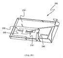
- FIG. 2A is a perspective view showing the top surface of an impedance transformation-type wide band antenna according to an embodiment of the present invention
- FIG. 2B is a perspective view showing the bottom surface of the impedance transformation-type wide band antenna according to an embodiment of the present invention.
- a radiation part 240 is made of a metallic plate formed in the shape of a rectangular parallelepiped, and part of one side surface extends, and thus a feeding part 220 and a short circuit part 290 are formed on the bottom surface of the radiation part 240.
- Stubs 250 defined by a plurality of slots 260 formed in the top surface and side surfaces of the radiation part 240 in the shape of a meandering line, are formed both on the top surface and side surfaces of the radiation part 240 to have a predetermined length, and are terminated with one ends thereof opened.
- the stubs 250 are divided into arbitrary shapes by the slots 260, and include a first stub 270 and a second stub 280.
- the feeding part 220 is adjacent to the short circuit part 290, and is formed to extend from the stubs 250 formed on the side surface of the radiation part 240 and to be bent multiple times in a " ⁇ "-shape, and to have a through hole 230 formed therein, thus a multi-path structure is implemented. Further, the feeding part 220 can be formed in a "2"-shape or various shapes within the height limitation.
- the feeding pin 210 is formed on the end of the feeding part 220 in the shape of a rectangle having a predetermined width.
- FIG. 3 is a graph showing the characteristics of the antenna of FIGS. 2A and 2B .
- the graph illustrates Standing Wave Ratio (SWR) characteristics of the antenna 200, and shows wide band characteristics.
- a frequency band for cellular communication which is currently commercialized is a band ranging from 800 MHz to 900 MHz
- a frequency band for Personal Communication Services (PCS) is a band ranging from 1700 MHz to 1900 MHz.
- a frequency band for International Mobile Telecommunications-2000 (IMT-2000) is a band ranging from 1900 MHz to 2200 MHz.
- IMT-2000 International Mobile Telecommunications-2000
- For an actual usage band for IMT-2000, a band of 230 MHz is assigned, and IMT-2000 must be operated in a wide band. If such characteristics are compared to those of the antenna 200 of the present invention, it can be seen that the wide band characteristics of the antenna are sufficiently learned, and the antenna of the present invention is utilized for a dual band or multiple band.
- the antenna of the present invention not only can cover respective bands, but also can be simultaneously used for different frequency bands, as a single antenna, in a wireless communication system that uses different frequency bands.
- the present invention provides an impedance transformation-type wide band antenna, which matches impedances using the length and interval of a feeding part, which is formed in a multi-path structure and is bent multiple times, the vertical distance between a short circuit part connected to an external ground and a radiation part, and the size of a through hole formed in the feeding part, so that a plurality of wide band resonant frequencies is formed, thus enabling the wide band antenna to be simultaneously used for different frequency bands, as a single antenna, in a wireless communication system that uses different frequency bands.
Description
- The present invention relates, in general, to an impedance transformation-type wide band internal antenna and, more particularly, to an impedance transformation-type wide band antenna, in which a feeding part is formed in a multi-path structure to transform impedance, and is bent multiple times to generate a plurality of resonant frequencies, thus enabling the impedance transformation-type wide band antenna to be used both in a multiple band and in a wide band.
- Currently, services for wireless communication have changed from narrow band communication services to wide band communication services, such as the Internet or multimedia. Further, due to the need to develop an integrated system capable of providing multiple services through a single terminal, the antennas of wireless communication systems are required to have wide band characteristics together with integrated functions.
-
FIG. 1A is a perspective view showing a conventional single layer wide band antenna using stubs, andFIG. 1B is a bottom view of the wide band antenna ofFIG. 1A . - As shown in
FIG. 1A , aconventional antenna 10 includes a dielectric(substrate) 20 provided on the upper portion thereof, apatch 40 formed on the dielectric 20 to have a width less than that of the dielectric 20 and to have ahole 30 formed therein, thin plate-shapedconductive stubs 50 attached to the diagonal corners of thepatch 40 and operated to transform the resonant frequency and impedance of theantenna 10 by converting the location and size of theconductive stubs 50, and aconductive ground plane 60 attached to the bottom surface of the dielectric 20. - As shown in
FIG. 1B , theantenna 10 includes acoaxial cable 80 that is soldered with afeeding point 70 through ahole 30 formed in thepatch 40 and is operated to provide an external signal source to thepatch 40. - The
patch 40 having a predetermined size is constructed in such a way that afirst stub 50, attached to the upper left portion of thepatch 40, and asecond stub 50, attached to the lower right portion of thepatch 40, are integrated with thepatch 40. In this case, wide band characteristics can be realized only when the locations of thestubs 50 are designed so as to be exactly symmetrical around the center of thepatch 40. If thestubs 50 are installed to be opposite each other, wide band characteristics cannot be realized in theantenna 10, and thus thestubs 50 are placed to be approximately symmetrical with each other around the center of thepatch 40. - Meanwhile, the dielectric 20, disposed between the
ground plane 60 and thepatch 40, which is a radiation element, can be filled with an air layer according to the purpose of theantenna 10. A connector required to feed theantenna 10 is also placed to be spaced apart from the center of theantenna 10 by a predetermined distance in the direction of one side thereof, so that the impedance of the antenna can be adjusted using the location of thefeeding point 70, together with the sizes of thestubs 50, thus obtaining wide band characteristics through impedance matching. - The conventional single layer wide band antenna using stubs is problematic in that, since the sizes of stubs or the location of a feeding point are changed so as to adjust the impedance thereof, there is a limitation in the space in which the antenna can actually be mounted in a wireless communication terminal, and since a multiple band must also be supported in the same antenna space, it is difficult to utilize such an antenna for a wireless communication system.
-
WO/2004/054034 discloses a multiple-band antenna having first and second operating frequency bands. The antenna includes a first patch structure associated primarily with the first operating frequency band, a second patch structure electrically coupled to the first patch structure and associated primarily with the second operating frequency band, a first slot structure disposed between a first portion of the first patch structure and the second patch structure and associated primarily with the first operating frequency band, and a second slot structure disposed between a second portion of the first patch structure and the second patch structure and associated with both the first operating frequency band and the second operating frequency band. - Accordingly, the present invention has been made keeping in mind the above problems occurring in the prior art, and an object of the present invention is to provide an impedance transformation-type wide band antenna, which is beneficial for the miniaturization of the main body thereof.
- Another object of the present invention is to provide an impedance transformation-type wide band antenna, in which a feeding part, formed in a multi-path structure, is bent multiple times, so that the height and length of the feeding part and the size of a through hole formed in the multi-path structure are adjusted to generate a plurality of resonant frequencies, thus enabling the antenna to be used both in a multiple band and in a wide band.
- In order to accomplish the above objects, the present invention provides an impedance transformation-type wide band antenna comprising; a radiation part formed to have a predetermined length and width according to an operating frequency, the radiation part including a plurality of stubs formed in arbitrary shape based on the location of a plurality of slots formed in a top surface and side surfaces of the radiation part; a short circuit part for causing part of a side surface of the radiation part to be connected to an external printed circuit board ground; a feeding part formed by a stub extending from one side of the top surface of the radiation part to be adjacent to the short circuit part; a feeding pin formed on an end of the feeding part, and
configured to be fed with current; where said feeding part, formed as a multi-path structure, is bent multiple times in a S-shape and has a through hole, so that the height and length of the feeding part and the size of the through hole are adjusted to generate a plurality of resonant frequencies. - Preferably, the feeding part may be designed so that impedances are matched using a length and interval of the feeding part, which is bent multiple times.
- Preferably, the feeding part may be formed to be bent in any one of a sideways u-shape or a backwards s-shape.
- Preferably, an inductance is introduced based on the length of the feeding part, and a capacitance is introduced based on an interval of the feeding part which is bent a multiple times.
- Preferably, an inductance is introduced based on a size of the through hole formed in the feeding part, thereby realizing broadband impedance matching.
- Preferably, the radiation part comprises a first stub for generating low resonant frequencies and a second stub for generating high resonant frequencies according to a terminated length of the stubs.
- The above and other objects, features and other advantages of the present invention will be more clearly understood from the following detailed description taken in conjunction with the accompanying drawings, in which:
-
FIG. 1A is a perspective view showing a conventional single layer wide band antenna using stubs; -
FIG. 1B is a bottom view showing the wide band antenna ofFIG. 1A ; -
FIG. 2A is a perspective view showing the top surface of an impedance transformation-type wide band antenna according to an embodiment of the present invention; -
FIG. 2B is a perspective view showing the bottom surface of the impedance transformation-type wide band antenna according to an embodiment of the present invention; and -
FIG. 3 is a graph showing the characteristics of the antenna ofFIG. 2 . - Hereinafter, embodiments of the present invention will be described in detail with reference to the attached drawings.
- Reference now should be made to the drawings, in which the same reference numerals are used throughout the different drawings to designate the same or similar components.
-
FIG. 2A is a perspective view showing the top surface of an impedance transformation-type wide band antenna according to an embodiment of the present invention, andFIG. 2B is a perspective view showing the bottom surface of the impedance transformation-type wide band antenna according to an embodiment of the present invention. - As shown in
FIGS. 2A and2B , aradiation part 240 is made of a metallic plate formed in the shape of a rectangular parallelepiped, and part of one side surface extends, and thus afeeding part 220 and ashort circuit part 290 are formed on the bottom surface of theradiation part 240. -
Stubs 250, defined by a plurality ofslots 260 formed in the top surface and side surfaces of theradiation part 240 in the shape of a meandering line, are formed both on the top surface and side surfaces of theradiation part 240 to have a predetermined length, and are terminated with one ends thereof opened. Thestubs 250 are divided into arbitrary shapes by theslots 260, and include afirst stub 270 and asecond stub 280. - The
short circuit part 290 is formed on the one side surface of theradiation part 240, adjacent to thefeeding part 220, to cause part of theshort circuit part 290 to be connected to an external ground. - The
feeding part 220 is adjacent to theshort circuit part 290, and is formed to extend from thestubs 250 formed on the side surface of theradiation part 240 and to be bent multiple times in a "⊏"-shape, and to have a throughhole 230 formed therein, thus a multi-path structure is implemented. Further, thefeeding part 220 can be formed in a "2"-shape or various shapes within the height limitation. - The
feeding pin 210 is formed on the end of thefeeding part 220 in the shape of a rectangle having a predetermined width. - The impedance transformation-type
wide band antenna 200 is fed with current through thefeeding pin 210 formed in the shape of a rectangle having a predetermined width. The current is adjusted using an inductance component corresponding to the length of thefeeding part 220, which is bent multiple times in a "⊏" shape and which is formed on part of the one side surface of theradiation part 240 made of a metallic plate having the shape of a rectangular parallelepiped, and the interval of thefeeding part 220, and thus the capacitance component and inductance component are formed. Accordingly, the multi-path structure changes the flow of current through the through hole formed in thefeeding part 220, thus forming inductance component. The flow of current is adjusted using the size of thethrough hole 230. - Further, the
short circuit part 290 is connected to the external ground, and thus components thereof are formed according to the vertical distance between theshort circuit part 290 and theradiation part 240, and the area of thefeeding part 220. Impedances are matched using the capacitance component and the inductance component, so that a plurality of wide band high resonant frequencies is generated. Through thefeeding part 220 in which impedances are matched, dual-band resonant frequencies are generated using the lengths of the first andsecond stubs slots 260, formed on the top and side surfaces of theradiation part 240, and which are formed on the top and side surfaces of theradiation part 240 to have predetermined lengths and are terminated with one ends thereof opened. -
FIG. 3 is a graph showing the characteristics of the antenna ofFIGS. 2A and2B . - As shown in
FIG. 3 , reflection characteristics for frequencies ranging from 700 MHz to 2300 MHz were measured for theantenna 200 ofFIG. 2 . The graph illustrates Standing Wave Ratio (SWR) characteristics of theantenna 200, and shows wide band characteristics. - A frequency band for cellular communication which is currently commercialized is a band ranging from 800 MHz to 900 MHz, and a frequency band for Personal Communication Services (PCS) is a band ranging from 1700 MHz to 1900 MHz. A frequency band for International Mobile Telecommunications-2000 (IMT-2000) is a band ranging from 1900 MHz to 2200 MHz. For an actual usage band for IMT-2000, a band of 230 MHz is assigned, and IMT-2000 must be operated in a wide band. If such characteristics are compared to those of the
antenna 200 of the present invention, it can be seen that the wide band characteristics of the antenna are sufficiently learned, and the antenna of the present invention is utilized for a dual band or multiple band. - That is, the antenna of the present invention not only can cover respective bands, but also can be simultaneously used for different frequency bands, as a single antenna, in a wireless communication system that uses different frequency bands.
- As described above, the present invention provides an impedance transformation-type wide band antenna, which matches impedances using the length and interval of a feeding part, which is formed in a multi-path structure and is bent multiple times, the vertical distance between a short circuit part connected to an external ground and a radiation part, and the size of a through hole formed in the feeding part, so that a plurality of wide band resonant frequencies is formed, thus enabling the wide band antenna to be simultaneously used for different frequency bands, as a single antenna, in a wireless communication system that uses different frequency bands.
Claims (4)
- An impedance transformation-type wide band antenna comprising:a radiation part (240) formed to have a predetermined length and width according to an operating frequency, the radiation part including a plurality of stubs formed in arbitrary shape based on the location of a plurality of slots (260) formed in a top surface and side surfaces of the radiation part;a short circuit part (290) for causing part of a side surface of the radiation part (240) to be connected to an external printed circuit board (PCB) ground;a feeding part (220) formed by a stub extending from one side of the top surface of the radiation part (240) to be adjacent to the short circuit part (290);a feeding pin (210) formed on an end of the feeding part (220), and configured to be fed with current;characterized in that
said feeding part, formed as a multi-path structure, is bent multiple times in a S-shape and has a through hole (230), so that the height and length of the feeding part (220) and the size of the through hole (230) are adjusted to generate a plurality of resonant frequencies. - The impedance transformation-type wide band antenna according to claim 1, wherein an inductance is introduced based on the length of the feeding part (220), and a capacitance is introduced based on an interval of the feeding part (220) which is bent a multiple times.
- The impedance transformation-type wide band antenna according to claim 2, wherein inductance is introduced based on a size of the through hole (230) formed in the feeding part (220), thereby realizing broadband impedance matching.
- The impedance transformation-type wide band antenna according to claim 1, wherein the radiation part (240) comprises a first stub (270) for generating low resonant frequencies and a second stub (280) for generating high resonant frequencies according to a terminated length of the stubs.
Applications Claiming Priority (1)
| Application Number | Priority Date | Filing Date | Title |
|---|---|---|---|
| KR1020050099343A KR100735154B1 (en) | 2005-10-20 | 2005-10-20 | Impedance Transformation Type Wide Band Antenna |
Publications (2)
| Publication Number | Publication Date |
|---|---|
| EP1777782A1 EP1777782A1 (en) | 2007-04-25 |
| EP1777782B1 true EP1777782B1 (en) | 2012-05-30 |
Family
ID=37671004
Family Applications (1)
| Application Number | Title | Priority Date | Filing Date |
|---|---|---|---|
| EP06020972A Expired - Fee Related EP1777782B1 (en) | 2005-10-20 | 2006-10-05 | Impedance transformation type wide band antenna |
Country Status (3)
| Country | Link |
|---|---|
| US (1) | US7619566B2 (en) |
| EP (1) | EP1777782B1 (en) |
| KR (1) | KR100735154B1 (en) |
Families Citing this family (6)
| Publication number | Priority date | Publication date | Assignee | Title |
|---|---|---|---|---|
| CN102104190A (en) * | 2009-12-21 | 2011-06-22 | 鸿富锦精密工业(深圳)有限公司 | Antenna and miniaturization method thereof |
| US9472846B2 (en) * | 2011-02-18 | 2016-10-18 | Laird Technologies, Inc. | Multi-band planar inverted-F (PIFA) antennas and systems with improved isolation |
| US10243251B2 (en) * | 2015-07-31 | 2019-03-26 | Agc Automotive Americas R&D, Inc. | Multi-band antenna for a window assembly |
| CN106972243B (en) * | 2017-01-22 | 2019-05-21 | 中国计量大学 | A kind of two-way coplanar 4G microstrip antenna of multiband covering GNSS |
| CN108666752A (en) * | 2018-04-17 | 2018-10-16 | 惠州市元盛科技有限公司 | A kind of flat plane antenna |
| CN108990315B (en) * | 2018-10-12 | 2021-04-06 | 郑州云海信息技术有限公司 | Differential via impedance control method |
Family Cites Families (10)
| Publication number | Priority date | Publication date | Assignee | Title |
|---|---|---|---|---|
| FI112723B (en) * | 1997-03-27 | 2003-12-31 | Nokia Corp | Antenna for wireless telephones |
| FI113212B (en) * | 1997-07-08 | 2004-03-15 | Nokia Corp | Dual resonant antenna design for multiple frequency ranges |
| DE10052909A1 (en) * | 2000-10-25 | 2002-05-08 | Siemens Ag | communication terminal |
| KR100423395B1 (en) * | 2001-07-02 | 2004-03-18 | 삼성전기주식회사 | A Chip Antenna |
| TW529779U (en) * | 2001-10-26 | 2003-04-21 | Hon Hai Prec Ind Co Ltd | Multi-frequency antenna |
| EP1372213A1 (en) * | 2002-06-11 | 2003-12-17 | Industrial Technology Research Institute | Multi-frequency band antenna |
| CN1695268A (en) * | 2002-11-28 | 2005-11-09 | 捷讯研究有限公司 | Multiple-band antenna with patch and slot structures |
| AU2002350334A1 (en) * | 2002-12-06 | 2004-06-30 | Research In Motion Limited | Multiple-band antenna with shared slot structure |
| US7102573B2 (en) * | 2003-01-13 | 2006-09-05 | Cushcraft Corporation | Patch antenna |
| JP4623272B2 (en) * | 2004-09-02 | 2011-02-02 | ミツミ電機株式会社 | Antenna device |
-
2005
- 2005-10-20 KR KR1020050099343A patent/KR100735154B1/en active IP Right Grant
-
2006
- 2006-10-05 EP EP06020972A patent/EP1777782B1/en not_active Expired - Fee Related
- 2006-10-20 US US11/551,398 patent/US7619566B2/en not_active Expired - Fee Related
Also Published As
| Publication number | Publication date |
|---|---|
| EP1777782A1 (en) | 2007-04-25 |
| US20070091000A1 (en) | 2007-04-26 |
| KR20070043274A (en) | 2007-04-25 |
| US7619566B2 (en) | 2009-11-17 |
| KR100735154B1 (en) | 2007-07-04 |
Similar Documents
| Publication | Publication Date | Title |
|---|---|---|
| US7564413B2 (en) | Multi-band antenna and mobile communication terminal having the same | |
| US7791541B2 (en) | Printed circuit board | |
| US7333067B2 (en) | Multi-band antenna with wide bandwidth | |
| US6404394B1 (en) | Dual polarization slot antenna assembly | |
| KR101031052B1 (en) | Multiband antenna component | |
| EP1018779B1 (en) | Planar dual-frequency antenna and radio apparatus employing a planar antenna | |
| US6677909B2 (en) | Dual band slot antenna with single feed line | |
| US7193576B2 (en) | Ultra wideband bow-tie slot antenna | |
| US7956812B2 (en) | Wide-band antenna and manufacturing method thereof | |
| JP2003163528A (en) | Printed circuit board, smd antenna, and communication equipment | |
| US7855686B2 (en) | Compact antennas for ultra-wideband applications | |
| US7230573B2 (en) | Dual-band antenna with an impedance transformer | |
| EP1777782B1 (en) | Impedance transformation type wide band antenna | |
| US9368858B2 (en) | Internal LC antenna for wireless communication device | |
| US20060290571A1 (en) | Ultra wide bandwidth planar antenna | |
| WO2000052783A1 (en) | Broadband antenna assembly of matching circuitry and ground plane conductive radiating element | |
| US8284116B2 (en) | Antenna apparatus for internal impedance matching | |
| JP2004512756A (en) | Broadband built-in antenna | |
| KR20020065811A (en) | Printed slot microstrip antenna with EM coupling feed system | |
| WO2002087012A1 (en) | Pifa antenna with higp structure | |
| US8159400B2 (en) | Chip antenna and mobile-communication terminal having the same | |
| KR20020091760A (en) | A built-in type antenna for a portable mobile | |
| KR100723682B1 (en) | CPW-fed planar inverted F-antenna with triple-bands for using mobile-phone | |
| US6717550B1 (en) | Segmented planar antenna with built-in ground plane | |
| KR20010088495A (en) | Small antenna of wireless data communication |
Legal Events
| Date | Code | Title | Description |
|---|---|---|---|
| PUAI | Public reference made under article 153(3) epc to a published international application that has entered the european phase |
Free format text: ORIGINAL CODE: 0009012 |
|
| AK | Designated contracting states |
Kind code of ref document: A1 Designated state(s): AT BE BG CH CY CZ DE DK EE ES FI FR GB GR HU IE IS IT LI LT LU LV MC NL PL PT RO SE SI SK TR |
|
| AX | Request for extension of the european patent |
Extension state: AL BA HR MK YU |
|
| 17P | Request for examination filed |
Effective date: 20070920 |
|
| 17Q | First examination report despatched |
Effective date: 20071025 |
|
| AKX | Designation fees paid |
Designated state(s): DE DK FI FR GB SE |
|
| RAP1 | Party data changed (applicant data changed or rights of an application transferred) |
Owner name: ACE ANTENNA CORP. |
|
| GRAP | Despatch of communication of intention to grant a patent |
Free format text: ORIGINAL CODE: EPIDOSNIGR1 |
|
| GRAS | Grant fee paid |
Free format text: ORIGINAL CODE: EPIDOSNIGR3 |
|
| GRAA | (expected) grant |
Free format text: ORIGINAL CODE: 0009210 |
|
| AK | Designated contracting states |
Kind code of ref document: B1 Designated state(s): DE DK FI FR GB SE |
|
| REG | Reference to a national code |
Ref country code: GB Ref legal event code: FG4D |
|
| REG | Reference to a national code |
Ref country code: DE Ref legal event code: R096 Ref document number: 602006029765 Country of ref document: DE Effective date: 20120726 |
|
| PG25 | Lapsed in a contracting state [announced via postgrant information from national office to epo] |
Ref country code: SE Free format text: LAPSE BECAUSE OF FAILURE TO SUBMIT A TRANSLATION OF THE DESCRIPTION OR TO PAY THE FEE WITHIN THE PRESCRIBED TIME-LIMIT Effective date: 20120530 Ref country code: FI Free format text: LAPSE BECAUSE OF FAILURE TO SUBMIT A TRANSLATION OF THE DESCRIPTION OR TO PAY THE FEE WITHIN THE PRESCRIBED TIME-LIMIT Effective date: 20120530 |
|
| PG25 | Lapsed in a contracting state [announced via postgrant information from national office to epo] |
Ref country code: DK Free format text: LAPSE BECAUSE OF FAILURE TO SUBMIT A TRANSLATION OF THE DESCRIPTION OR TO PAY THE FEE WITHIN THE PRESCRIBED TIME-LIMIT Effective date: 20120530 |
|
| PLBE | No opposition filed within time limit |
Free format text: ORIGINAL CODE: 0009261 |
|
| STAA | Information on the status of an ep patent application or granted ep patent |
Free format text: STATUS: NO OPPOSITION FILED WITHIN TIME LIMIT |
|
| 26N | No opposition filed |
Effective date: 20130301 |
|
| REG | Reference to a national code |
Ref country code: DE Ref legal event code: R097 Ref document number: 602006029765 Country of ref document: DE Effective date: 20130301 |
|
| REG | Reference to a national code |
Ref country code: FR Ref legal event code: PLFP Year of fee payment: 10 |
|
| REG | Reference to a national code |
Ref country code: FR Ref legal event code: PLFP Year of fee payment: 11 |
|
| REG | Reference to a national code |
Ref country code: FR Ref legal event code: PLFP Year of fee payment: 12 |
|
| PGFP | Annual fee paid to national office [announced via postgrant information from national office to epo] |
Ref country code: FR Payment date: 20171010 Year of fee payment: 12 Ref country code: DE Payment date: 20171002 Year of fee payment: 12 |
|
| PGFP | Annual fee paid to national office [announced via postgrant information from national office to epo] |
Ref country code: GB Payment date: 20171002 Year of fee payment: 12 |
|
| REG | Reference to a national code |
Ref country code: DE Ref legal event code: R119 Ref document number: 602006029765 Country of ref document: DE |
|
| GBPC | Gb: european patent ceased through non-payment of renewal fee |
Effective date: 20181005 |
|
| PG25 | Lapsed in a contracting state [announced via postgrant information from national office to epo] |
Ref country code: DE Free format text: LAPSE BECAUSE OF NON-PAYMENT OF DUE FEES Effective date: 20190501 |
|
| PG25 | Lapsed in a contracting state [announced via postgrant information from national office to epo] |
Ref country code: FR Free format text: LAPSE BECAUSE OF NON-PAYMENT OF DUE FEES Effective date: 20181031 |
|
| PG25 | Lapsed in a contracting state [announced via postgrant information from national office to epo] |
Ref country code: GB Free format text: LAPSE BECAUSE OF NON-PAYMENT OF DUE FEES Effective date: 20181005 |