EP1777490A2 - Methods and apparatus for inspecting an object using structured light - Google Patents
Methods and apparatus for inspecting an object using structured light Download PDFInfo
- Publication number
- EP1777490A2 EP1777490A2 EP06255432A EP06255432A EP1777490A2 EP 1777490 A2 EP1777490 A2 EP 1777490A2 EP 06255432 A EP06255432 A EP 06255432A EP 06255432 A EP06255432 A EP 06255432A EP 1777490 A2 EP1777490 A2 EP 1777490A2
- Authority
- EP
- European Patent Office
- Prior art keywords
- light
- lens
- grating
- structured light
- dmd
- Prior art date
- Legal status (The legal status is an assumption and is not a legal conclusion. Google has not performed a legal analysis and makes no representation as to the accuracy of the status listed.)
- Withdrawn
Links
Images



Classifications
-
- G—PHYSICS
- G01—MEASURING; TESTING
- G01B—MEASURING LENGTH, THICKNESS OR SIMILAR LINEAR DIMENSIONS; MEASURING ANGLES; MEASURING AREAS; MEASURING IRREGULARITIES OF SURFACES OR CONTOURS
- G01B11/00—Measuring arrangements characterised by the use of optical techniques
- G01B11/24—Measuring arrangements characterised by the use of optical techniques for measuring contours or curvatures
- G01B11/25—Measuring arrangements characterised by the use of optical techniques for measuring contours or curvatures by projecting a pattern, e.g. one or more lines, moiré fringes on the object
- G01B11/2513—Measuring arrangements characterised by the use of optical techniques for measuring contours or curvatures by projecting a pattern, e.g. one or more lines, moiré fringes on the object with several lines being projected in more than one direction, e.g. grids, patterns
Definitions
- This application relates generally to inspecting objects, and more specifically to methods and apparatus for inspecting objects using a light measurement system.
- Objects are sometimes inspected, for example, to determine a size and/or shape of all or a portion of the object and/or to detect defects in the object.
- some gas turbine engine components such as turbine or compressor blades, are inspected to detect fatigue cracks that may be caused by vibratory, mechanical, and/or thermal stresses induced to the engine.
- some gas turbine engine blades are inspected for deformations such as platform orientation, contour cross-section, bow and twist along a stacking axis, thickness, and/or chord length at given cross-sections.
- deformations such as platform orientation, contour cross-section, bow and twist along a stacking axis, thickness, and/or chord length at given cross-sections.
- continued operation of the object with one or more defects may reduce performance of the object and/or lead to object failures, for example, as cracks propagate through the object. Accordingly, detecting defects of the object as early as possible may facilitate increasing the performance of the object and/or reducing object failures.
- At least some objects are inspected using a light measurement system that projects a structured light pattern onto a surface of the object.
- the light measurement system images the structured light pattern reflected from the surface of the object and then analyzes the deformation of the reflected light pattern to calculate surface features of the object.
- at least some known light measurement systems are unable to adjust distribution of light over different areas of the illuminated surface of the object, possibly causing some areas of the illuminated surface to be too dark or too light to inspect.
- Some known light measurement systems utilize liquid crystal display (LCD), liquid crystal on silicon (LCOS), or digital micromirror device (DMD) devices as light sources that can adjust distribution of light over different areas of the illuminated object surface.
- LCD liquid crystal display
- LCOS liquid crystal on silicon
- DMD digital micromirror device
- At least some known LCD, LCOS, and DMD devices may have lower resolution than is desired for the light source. Moreover, at least some known LCD, LCOS, and DMD devices may not be capable of accurately constructing a smooth pattern of light, for example a sine wave, but rather may create a binary approximation. Film-type attenuators have also been used to control distribution of light over different areas of the illuminated surface of the object, for example to darken areas of the illuminated surface that may be too light to measure. However, at least some known attenuators may need to be changed when a different object is inspected and/or when the object, a light source, and/or an imaging sensor is re-orientated.
- a method for inspecting an object using a light measurement system that includes a light source and an imaging sensor.
- the method includes emitting light from the light source, dispersing light emitted from the light source into one of a diffraction pattern and an interference pattern, and imaging the patterned light onto the object using a lens.
- a structured light measurement system for inspecting an object includes a structured light source configured to project structured light onto a surface of the object, an imaging sensor configured to receive structured light reflected from the object surface, a grating positioned to disperse light emitted by the structured light source into at least one of a diffraction pattern and an interference pattern, and a lens positioned to image patterned light received from the grating onto the object.
- a structured light measurement system for inspecting an object includes a laser configured to project structured light onto a surface of the object, an imaging sensor configured to receive structured light reflected from the object surface, a beam splitter positioned at least partially between the laser and the object for dispersing light emitted by the laser into an interference pattern, and a lens positioned to image patterned light received from the beam splitter onto the object.
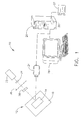
- Figure 1 is a block diagram of an exemplary embodiment of a structured light measurement system 10 that is used to measure a plurality of surface features of an object 12.
- system 10 may be used to inspect and determine surfaces of object 12, wherein the surfaces may include features such as tilts, bends, twists, and/or warps when compared to a model representative of object 12.
- object 12 is a rotor blade, such as, but not limited to, a compressor or turbine blade utilized in a turbine engine. Accordingly, and in the exemplary embodiment, object 12 includes an airfoil 14 extending outwardly from a platform 16. While the following description is directed to inspecting gas turbine engine blades, one skilled in the art will appreciate that system 10 may be utilized to improve structured light imaging for any object.
- System 10 includes a structured light source 22 such as, but not limited to, a white light lamp, a laser, a light emitting diode (LED), a liquid crystal display (LCD) device, a liquid crystal on silicon (LCOS) device, and/or a digital micromirror device (DMD).
- System 10 also includes one or more imaging sensors 24 that receive structured light reflected from object 12.
- imaging sensor 24 is a camera that receives and creates images using structured light reflected from object 12, although system 10 may utilize other imaging sensors 24.
- One or more computers 26 process images received from sensors 24, and a monitor 28 may be utilized to display information to an operator.
- computer(s) 26 include a device 30, for example, a floppy disk drive, CD-ROM drive, DVD drive, magnetic optical disk (MOD) device, and/or any other digital device including a network connecting device such as an Ethernet device for reading instructions and/or data from a computer-readable medium 32, such as a floppy disk, a CD-ROM, a DVD, and/or another digital source such as a network or the Internet, as well as yet to be developed digital means.
- computer(s) 26 execute instructions stored in firmware (not shown).
- Computer(s) 26 are programmed to perform functions described herein, and as used herein, the term computer is not limited to just those integrated circuits referred to in the art as computers, but broadly refers to computers, processors, microcontrollers, microcomputers, programmable logic controllers, application specific integrated circuits, and other programmable circuits, and these terms are used interchangeably herein.
- System 10 also includes a lens 34, a grating 36, and a lens 38.
- lens 34 is a field lens, such as, but not limited to, a biconvex lens.
- Lens 34 is positioned at least partially between light source 22 and grating 36, and receives and channels light emitted from light source 22 through grating 36.
- Grating 36 is positioned at least partially between lens 34 and lens 38 and, in some embodiments, includes a pattern (not shown) that disperses light channeled therethrough into a diffraction pattern. More specifically, in some embodiments, grating 36 includes a pattern of lines and spaces formed on a substrate for dispersing light into a diffraction pattern.
- grating 36 includes a pattern of periodic lines and spaces, such as, for example, a ronchi ruling. Although grating 36 may have other patterns, in some embodiments grating 36 includes lines that each have a width between about 10 and about 15 microns, such that the pattern includes between about 50 and about 100 line pairs per millimeter. In other embodiments, grating 36 includes a pattern of lines and spaces wherein the spaces between lines becomes successively smaller adjacent an edge of grating 36, such as, for example, a rectangular slit diffraction pattern. The pattern of lines and spaced may be formed on the substrate using any suitable method and/or structure.
- the pattern of lines and spaces is formed from a plurality of strands of material, such as, but not limited to metal strands (e.g., chrome strands), attached to and/or embedded within the substrate.
- the pattern of lines and spaces is etched into the substrate.
- Each etched line in some embodiments, may be filled with a suitable material, such as, but not limited to, metal (e.g., chrome).
- the substrate of grating 36 may be fabricated from other materials, in some embodiments the substrate of grating 36 is fabricated from glass and/or quartz.
- grating 36 includes a pattern (not shown) that disperses light channeled therethrough into an interference pattern, such as, but not limited to, a uniform sine wave pattern of evenly spaced lines.
- grating 36 is a phase grating, such as, but not limited to, a photographic recording of a simple series of square lines that has been bleached such that no intensity pattern in seen directly on the recording, but small refractive index changes left on the recording where the lines existed serve as a series of prisms to redirect the light at some plus and minus angle that will then interfere to create an interference pattern.
- Lens 38 receives and images the patterned light onto object 12 to illuminate object 12 with light emitted from light source 22.
- lens 38 is a "high-resolution" lens, or more specifically, a lens that facilitates generating an image having a contrast of greater than about 50%.
- lens 38 is flat field lens, such as, but not limited to, an enlarger lens and/or a lithographic lens.
- light source 22 includes an LCD, a LCOS, and/or a DMD device.
- Some other known light sources for example, lasers, light emitting diodes (LEDs), and white light lamps, are unable to adjust distribution of light over different areas of an illuminated surface of object 12. More specifically, some of such other known light sources may be unable to adjust the level of light projected onto different areas of the illuminated surface of object 12. Accordingly, some areas of the illuminated object surface may be too dark or too light to inspect using light sources other than LCD, LCOS, and/or DMD devices.
- some known LCD, LCOS, and DMD devices are capable of adjusting distribution of light emitted therefrom.
- system 10 can adjust a distribution of light levels projected onto different areas of the illuminated surface of object 12.
- some known LCD, LCOS, and DMD devices may project a lower resolution of light onto object 12 than is desired and/or suitable for inspecting object 12.
- some known LCD, LCOS, and DMD devices may not be capable of accurately constructing a smooth pattern of light, for example a sine wave, but rather may create a binary approximation.
- system 10 facilitates illuminating object 12 with a smooth pattern of light and facilitates increasing a resolution of light reflected from object 12, as compared to known light measurement systems using LCD, LCOS, and/or DMD devices. More specifically, as light passes through grating 36, grating 36 facilitates dispersing light emitted from light source 22 into a smooth pattern of light, for example, a smooth diffraction or interference pattern.
- grating 36 When grating 36 includes a pattern of lines and spaces, the size of the lines and spaces, in combination with a contrast generated by lens 38, can be selected to increase a resolution of light reflected from object 12, as compared to known light measurement systems using LCD, LCOS, and/or DMD devices. Moreover, when grating 36 is a phase grating, the interference created by grating 36, in combination with a contrast generated by lens 38, can be selected to increase a resolution of light reflected from object 12, as compared to known light measurement systems using LCD, LCOS, and/or DMD devices.
- light source 22 includes an LCD, LCOS, and/or DMD device
- system 10 can adjust light levels projected onto different areas of the illuminated surface of object 12. Accordingly, areas of the illuminated surface of object 12 that are too light or too dark can be adjusted such that they are measurable by system 10, and more specifically viewable by imaging sensor 24.
- an electronic and/or physical mask may be used in combination with light source 22 to facilitate precluding light source 22 from illuminating surfaces at locations other than a portion of object 12 that is to be inspected. Such a mask may thereby facilitate reducing inter-reflections between surrounding structure, for example a test fixture, and surfaces of object 12 to be inspected.
- such a mask may facilitate producing an illumination pattern on object 12 that substantially matches a profile of a portion of object 12 to be inspected, as viewed from the location of light source 22.
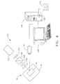
- Figure 2 is a block diagram of an alternative embodiment of a structured light measurement system 50 that is used to measure a plurality of surface features of object 12. More specifically, system 50 is used to inspect and determine surfaces of object 12, wherein the surfaces may include features such as tilts, bends, twists, and/or warps when compared to a model representative of object 12.
- object 12 is a rotor blade, such as, but not limited to, a compressor or turbine blade utilized in a turbine engine. Accordingly, and in the exemplary embodiment, object 12 includes airfoil 14 extending outwardly from platform 16. While the following description is directed to inspecting gas turbine engine blades, one skilled in the art will appreciate that system50 may be utilized to improve structured light imaging for any object.
- System 50 includes a structured light source 52, such as, but not limited to, a laser, a white light lamp, a light emitting diode (LED), a liquid crystal display (LCD) device, a liquid crystal on silicon (LCOS) device, and/or a digital micromirror device (DMD).
- System 50 also includes one or more imaging sensors 54 that receive structured light reflected from object 12.
- imaging sensor 54 is a camera that receives and creates images using structured light reflected from object 12, although system 50 may utilize other imaging sensors 54.
- One or more computers 56 process images received from sensors 54, and a monitor 58 may be utilized to display information to an operator.
- computer(s) 56 include a device 60, for example, a floppy disk drive, CD-ROM drive, DVD drive, magnetic optical disk (MOD) device, and/or any other digital device including a network connecting device such as an Ethernet device for reading instructions and/or data from a computer-readable medium 62, such as a floppy disk, a CD-ROM, a DVD, and/or another digital source such as a network or the Internet, as well as yet to be developed digital means.
- computer(s) 56 execute instructions stored in firmware (not shown).
- Computer(s) 56 are programmed to perform functions described herein, and as used herein, the term computer is not limited to just those integrated circuits referred to in the art as computers, but broadly refers to computers, processors, microcontrollers, microcomputers, programmable logic controllers, application specific integrated circuits, and other programmable circuits, and these terms are used interchangeably herein.
- System 50 also includes a lens 64, a grating 66, a liquid crystal display (LCD) device 68, and a lens 70.
- lens 64 is a field lens, such as, but not limited to, a biconvex lens.
- Lens 64 is positioned at least partially between light source 52 and grating 66, and receives and channels light emitted from light source 52 through grating 66.
- Grating 66 is positioned at least partially between lens 64 and LCD device 68 and, in some embodiments, includes a pattern (not shown) that disperses light channeled therethrough into a diffraction pattern.
- grating 66 includes a pattern of lines and spaces formed on a substrate for dispersing light into a diffraction pattern.
- grating 66 includes a pattern of periodic lines and spaces, such as, for example, a ronchi ruling.
- grating 66 may have other patterns, in some embodiments grating 66 includes lines that each have a width between about 10 and about 15 microns, such that the pattern includes between about 50 and about 100 line pairs per millimeter.
- grating 36 includes a pattern of lines and spaces wherein the spaces between lines becomes successively smaller adjacent an edge of grating 36, such as, for example, a rectangular slit diffraction pattern.
- the pattern of lines and spaced may be formed on the substrate using any suitable method and/or structure.
- the pattern of lines and spaces is formed from a plurality of strands of material, such as, but not limited to metal strands (e.g., chrome strands), attached to and/or embedded within the substrate.
- the pattern of lines and spaces is etched into the substrate.
- Each etched line in some embodiments, may be filled with a suitable material, such as, but not limited to, metal (e.g., chrome).
- the substrate of grating 66 may be fabricated from other materials, in some embodiments the substrate of grating 66 is fabricated from glass and/or quartz.
- grating 36 includes a pattern (not shown) that disperses light channeled therethrough into an interference pattern, such as, but not limited to, a uniform sine wave pattern of evenly spaced lines.
- grating 36 is a phase grating, such as, but not limited to, a photographic recording of a simple series of square lines that has been bleached such that no intensity pattern in seen directly on the recording, but small refractive index changes left on the recording where the lines existed serve as a series of prisms to redirect the light at some plus and minus angle that will then interfere to create an interference pattern.
- Patterned light dispersed from grating 66 is channeled through LCD device 68 for, for example, control of light distribution and/or masking.
- Lens 70 receives and images the patterned light onto object 12 to illuminate object 12 with light emitted from light source 52.
- lens 70 is a "high-resolution" lens, or more specifically, a lens that facilitates generating an image having a contrast of greater than about 50%.
- lens 70 is flat field lens, such as, but not limited to, an enlarger lens and/or a lithographic lens.
- system 50 facilitates illuminating object 12 with a smooth pattern of light and facilitates increasing a resolution of light reflected from object 12, as compared to known light measurement systems using LCD, LCOS, and/or DMD devices as light sources. More specifically, as light passes through grating 66, grating 66 facilitates dispersing light emitted from light source 52 into a smooth pattern of light, for example, a smooth diffraction or interference pattern.
- grating 66 When grating 66 includes a pattern of lines and spaces, the size of the lines and spaces, in combination with a contrast generated by lens 70, can be selected to increase a resolution of light reflected from object 12, as compared to known light measurement systems using LCD, LCOS, and/or DMD devices as light sources. Moreover, when grating 66 is a phase grating, the interference created by grating 66, in combination with a contrast generated by lens 70, can be selected to increase a resolution of light reflected from object 12, as compared to known light measurement systems using LCD, LCOS, and/or DMD devices.
- system 50 can adjust light levels projected onto different areas of the illuminated surface of object 12. Accordingly, areas of the illuminated surface of object 12 that are too light or too dark can be adjusted such that they are measurable by system 50, and more specifically viewable by imaging sensor 54.
- an electronic and/or physical mask may be used in combination with light source 52 and/or LCD device 68 to facilitate precluding light source 52 from illuminating surfaces at locations other than a portion of object 12 that is to be inspected. Such a mask may thereby facilitate reducing inter-reflections between surrounding structure, for example a test fixture, and surfaces of object 12 to be inspected.
- such a mask may facilitate producing an illumination pattern on object 12 that substantially matches a profile of a portion of object 12 to be inspected, as viewed from the location of light source 52.
- system 50 may facilitate increasing an operational life of LCD device 68.
- Figure 3 is a block diagram of another embodiment of a structured light measurement system 80 that is used to measure a plurality of surface features of object 12. More specifically, system 80 is used to inspect and determine surfaces of object 12, wherein the surfaces may include features such as tilts, bends, twists, and/or warps when compared to a model representative of object 12.
- object 12 is a rotor blade, such as, but not limited to, a compressor or turbine blade utilized in a turbine engine. Accordingly, and in the exemplary embodiment, object 12 includes airfoil 14 extending outwardly from platform 16. While the following description is directed to inspecting gas turbine engine blades, one skilled in the art will appreciate that system 80 may be utilized to improve structured light imaging for any object.
- System 80 includes a structured light source 82, such as, but not limited to, a laser, a white light lamp, a light emitting diode (LED), a liquid crystal display (LCD) device, a liquid crystal on silicon (LCOS) device, and/or a digital micromirror device (DMD).
- System 80 also includes one or more imaging sensors 84 that receive structured light reflected from object 12.
- imaging sensor 84 is a camera that receives and creates images using structured light reflected from object 12, although system 80 may utilize other imaging sensors 84.
- One or more computers 86 process images received from sensors 84, and a monitor 88 may be utilized to display information to an operator.
- computer(s) 86 include a device 90, for example, a floppy disk drive, CD-ROM drive, DVD drive, magnetic optical disk (MOD) device, and/or any other digital device including a network connecting device such as an Ethernet device for reading instructions and/or data from a computer-readable medium 92, such as a floppy disk, a CD-ROM, a DVD, and/or another digital source such as a network or the Internet, as well as yet to be developed digital means.
- computer(s) 86 execute instructions stored in firmware (not shown).
- Computer(s) 86 are programmed to perform functions described herein, and as used herein, the term computer is not limited to just those integrated circuits referred to in the art as computers, but broadly refers to computers, processors, microcontrollers, microcomputers, programmable logic controllers, application specific integrated circuits, and other programmable circuits, and these terms are used interchangeably herein.
- System 80 also includes a lens 94, a grating 96, a mirror 98, a digital micromirror device (DMD) 100, and a lens 102.
- lens 94 is a field lens, such as, but not limited to, a biconvex lens.
- Lens 94 is positioned at least partially between light source 82 and grating 96, and receives and channels light emitted from light source 82 through grating 96.
- Grating 96 is positioned at least partially between lens 94 and mirror 98 and, in some embodiments, includes a pattern (not shown) that disperses light channeled therethrough into a diffraction pattern.
- grating 96 includes a pattern of lines and spaces formed on a substrate for dispersing light into a diffraction pattern.
- grating 96 includes a pattern of periodic lines and spaces, such as, for example, a ronchi ruling.
- grating 96 may have other patterns, in some embodiments grating 96 includes lines that each have a width between about 10 and about 15 microns, such that the pattern includes between about 50 and about 100 line pairs per millimeter.
- grating 36 includes a pattern of lines and spaces wherein the spaces between lines becomes successively smaller adjacent an edge of grating 36, such as, for example, a rectangular slit diffraction pattern.
- the pattern of lines and spaced may be formed on the substrate using any suitable method and/or structure.
- the pattern of lines and spaces is formed from a plurality of strands of material, such as, but not limited to metal strands (e.g., chrome strands), attached to and/or embedded within the substrate.
- the pattern of lines and spaces is etched into the substrate.
- Each etched line in some embodiments, may be filled with a suitable material, such as, but not limited to, metal (e.g., chrome).
- the substrate of grating 96 may be fabricated from other materials, in some embodiments the substrate of grating 96 is fabricated from glass and/or quartz.
- grating 36 includes a pattern (not shown) that disperses light channeled therethrough into an interference pattern, such as, but not limited to, a uniform sine wave pattern of evenly spaced lines.
- grating 36 is a phase grating, such as, but not limited to, a photographic recording of a simple series of square lines that has been bleached such that no intensity pattern in seen directly on the recording, but small refractive index changes left on the recording where the lines existed serve as a series of prisms to redirect the light at some plus and minus angle that will then interfere to create an interference pattern.
- Patterned light dispersed from grating 96 is reflected off mirror 98 and directed toward DMD 100 for, for example, control of light distribution and/or masking.
- mirror 98 is a half-silver mirror.
- Light reflected off DMD 100 is channeled through mirror 98 and received by lens 102.
- a wave plate 104 is positioned between DMD 100 and mirror 98 to facilitate reducing a loss of light reflected off mirror 98 and DMD 100.
- Lens 102 receives and images the patterned light onto object 12 to illuminate object 12 with light emitted from light source 82.
- lens 102 is a "high-resolution" lens, or more specifically, a lens that facilitates generating an image having a contrast of greater than about 50%.
- lens 102 is flat field lens, such as, but not limited to, an enlarger lens and/or a lithographic lens.
- system 80 facilitates illuminating object 12 with a smooth pattern of light and facilitates increasing a resolution of light reflected from object 12, as compared to known light measurement systems using LCD, LCOS, and/or DMD devices as light sources. More specifically, as light passes through grating 96, grating 96 facilitates dispersing light emitted from light source 82 into a smooth pattern of light, for example, a smooth diffraction or interference pattern.
- grating 96 When grating 96 includes a pattern of lines and spaces, the size of the lines and spaces, in combination with a contrast generated by lens 102, can be selected to increase a resolution of light reflected from object 12, as compared to known light measurement systems using LCD and/or DMD projectors as light sources. Moreover, when grating 96 is a phase grating, the interference created by grating 96, in combination with a contrast generated by lens 102, can be selected to increase a resolution of light reflected from object 12, as compared to known light measurement systems using LCD, LCOS, and/or DMD devices.
- system 80 can adjust light levels projected onto different areas of the illuminated surface of object 12. Accordingly, areas of the illuminated surface of object 12 that are too light or too dark can be adjusted such that they are measurable by system 80, and more specifically viewable by imaging sensor 84.
- an electronic and/or physical mask may be used in combination with light source 82 and/or DMD 100 to facilitate precluding light source 82 from illuminating surfaces at locations other than a portion of object 12 that is to be inspected. Such a mask may thereby facilitate reducing inter-reflections between surrounding structure, for example a test fixture, and surfaces of object 12 to be inspected.
- such a mask may facilitate producing an illumination pattern on object 12 that substantially matches a profile of a portion of object 12 to be inspected, as viewed from the location of light source 82.
- system 80 may facilitate increasing an operational life of DMD 100.
- Figure 4 is a block diagram of another embodiment of a structured light measurement system 110 that is used to measure a plurality of surface features of object 12. More specifically, system 110 is used to inspect and determine surfaces of object 12, wherein the surfaces may include features such as tilts, bends, twists, and/or warps when compared to a model representative of object 12.
- object 12 is a rotor blade, such as, but not limited to, a compressor or turbine blade utilized in a turbine engine. Accordingly, and in the exemplary embodiment, object 12 includes airfoil 14 extending outwardly from platform 16. While the following description is directed to inspecting gas turbine engine blades, one skilled in the art will appreciate that system 110 may be utilized to improve structured light imaging for any object.
- System 110 includes a laser 112 and one or more imaging sensors 114 that receive structured light reflected from object 12.
- imaging sensor 114 is a camera that receives and creates images using structured light reflected from object 12, although system 110 may utilize other imaging sensors 114.
- One or more computers 116 process images received from sensors 114, and a monitor 118 may be utilized to display information to an operator.
- computer(s) 116 include a device 120, for example, a floppy disk drive, CD-ROM drive, DVD drive, magnetic optical disk (MOD) device, and/or any other digital device including a network connecting device such as an Ethernet device for reading instructions and/or data from a computer-readable medium 122, such as a floppy disk, a CD-ROM, a DVD, and/or another digital source such as a network or the Internet, as well as yet to be developed digital means.
- computer(s) 56 execute instructions stored in firmware (not shown).
- Computer(s) 116 are programmed to perform functions described herein, and as used herein, the term computer is not limited to just those integrated circuits referred to in the art as computers, but broadly refers to computers, processors, microcontrollers, microcomputers, programmable logic controllers, application specific integrated circuits, and other programmable circuits, and these terms are used interchangeably herein.
- System 110 also includes a lens 124, a beam splitter 126, a liquid crystal display (LCD) device 128, and a lens 130.
- lens 124 is a field lens, such as, but not limited to, a biconvex lens.
- Lens 124 is positioned at least partially between laser 112 and beam splitter 126, and receives and channels light emitted from laser 112 to beam splitter 126.
- Beam splitter 126 is positioned to disperse light emitted from laser 112 into an interference pattern by splitting and recombining the light.
- beam splitter 126 is a half-silver mirror.
- Patterned light dispersed from beam splitter 126 is channeled through LCD device 128 for, for example, control of light distribution and/or masking.
- Lens 130 receives and images the patterned light onto object 12 to illuminate object 12 with light emitted from laser 112.
- lens 130 is a "high-resolution" lens, or more specifically, a lens that facilitates generating an image having a contrast of greater than about 50%.
- lens 130 is flat field lens, such as, but not limited to, an enlarger lens and/or a lithographic lens.
- system 110 facilitates illuminating object 12 with a smooth pattern of light and facilitates increasing a resolution of light reflected from object 12, as compared to known light measurement systems using LCD, LCOS, and/or DMD devices as light sources. More specifically, beam splitter 126 facilitates dispersing light emitted from laser 112 into a smooth interference pattern of light.
- the interference created by beam splitter 126, in combination with a contrast generated by lens 130, can be selected to increase a resolution of light reflected from object 12, as compared to known light measurement systems using LCD, LCOS, and/or DMD devices.
- system 110 can adjust light levels projected onto different areas of the illuminated surface of object 12. Accordingly, areas of the illuminated surface of object 12 that are too light or too dark can be adjusted such that they are measurable by system 110, and more specifically viewable by imaging sensor 114.
- an electronic and/or physical mask may be used in combination with laser 112 and/or LCD device 128 to facilitate precluding laser 112 from illuminating surfaces at locations other than a portion of object 12 that is to be inspected. Such a mask may thereby facilitate reducing inter-reflections between surrounding structure, for example a test fixture, and surfaces of object 12 to be inspected.
- such a mask may facilitate producing an illumination pattern on object 12 that substantially matches a profile of a portion of object 12 to be inspected, as viewed from the location of laser 112.
- system 110 may facilitate increasing an operational life of LCD device 128.
- Figure 5 is a block diagram of another embodiment of a structured light measurement system 150 that is used to measure a plurality of surface features of object 12. More specifically, system 150 is used to inspect and determine surfaces of object 12, wherein the surfaces may include features such as tilts, bends, twists, and/or warps when compared to a model representative of object 12.
- object 12 is a rotor blade, such as, but not limited to, a compressor or turbine blade utilized in a turbine engine. Accordingly, and in the exemplary embodiment, object 12 includes airfoil 14 extending outwardly from platform 16. While the following description is directed to inspecting gas turbine engine blades, one skilled in the art will appreciate that system 150 may be utilized to improve structured light imaging for any object.
- System 150 includes a laser 152 and one or more imaging sensors 154 that receive structured light reflected from object 12.
- imaging sensor 154 is a camera that receives and creates images using structured light reflected from object 12, although system 150 may utilize other imaging sensors 154.
- One or more computers 156 process images received from sensors 154, and a monitor 158 may be utilized to display information to an operator.
- computer(s) 156 include a device 160, for example, a floppy disk drive, CD-ROM drive, DVD drive, magnetic optical disk (MOD) device, and/or any other digital device including a network connecting device such as an Ethernet device for reading instructions and/or data from a computer-readable medium 162, such as a floppy disk, a CD-ROM, a DVD, and/or another digital source such as a network or the Internet, as well as yet to be developed digital means.
- computer(s) 156 execute instructions stored in firmware (not shown).
- Computer(s) 156 are programmed to perform functions described herein, and as used herein, the term computer is not limited to just those integrated circuits referred to in the art as computers, but broadly refers to computers, processors, microcontrollers, microcomputers, programmable logic controllers, application specific integrated circuits, and other programmable circuits, and these terms are used interchangeably herein.
- System 150 also includes a lens 164, a beam splitter 166, a mirror 168, a digital micromirror device (DMD) 170, and a lens 172.
- lens 164 is a field lens, such as, but not limited to, a biconvex lens.
- Lens 164 is positioned at least partially between laser 152 and beam splitter 166, and receives and channels light emitted from laser 152 to beam splitter 166.
- Beam splitter 166 is positioned to disperse light emitted from laser 152 into an interference pattern by splitting and recombining the light.
- beam splitter 166 is a half-silver mirror.
- Patterned light dispersed from beam splitter 166 is reflected off mirror 168 and directed towards DMD 170 for, for example, control of light distribution and/or masking.
- mirror 168 is a half-silver mirror.
- Light reflected off DMD 170 is channeled through mirror 168 and received by lens 172.
- a wave plate 174 is positioned between DMD 170 and mirror 168 to facilitate reducing a loss of light reflected off mirror 168 and DMD 170.
- Lens 172 receives and images the patterned light onto object 12 to illuminate object 12 with light emitted from laser 152.
- lens 172 is a "high-resolution" lens, or more specifically, a lens that facilitates generating an image having a contrast of greater than about 50%.
- lens 172 is flat field lens, such as, but not limited to, an enlarger lens and/or a lithographic lens.
- system 150 facilitates illuminating object 12 with a smooth pattern of light and facilitates increasing a resolution of light reflected from object 12, as compared to known light measurement systems using LCD, LCOS, and/or DMD devices as light sources. More specifically, beam splitter 166 facilitates dispersing light emitted from laser 152 into a smooth interference pattern of light.
- the interference created by beam splitter 166, in combination with a contrast generated by lens 172, can be selected to increase a resolution of light reflected from object 12, as compared to known light measurement systems using LCD, LCOS, and/or DMD devices.
- system 150 can adjust light levels projected onto different areas of the illuminated surface of object 12. Accordingly, areas of the illuminated surface of object 12 that are too light or too dark can be adjusted such that they are measurable by system 150, and more specifically viewable by imaging sensor 154.
- an electronic and/or physical mask may be used in combination with laser 152 and/or DMD 170 to facilitate precluding laser 152 from illuminating surfaces at locations other than a portion of object 12 that is to be inspected. Such a mask may thereby facilitate reducing inter-reflections between surrounding structure, for example a test fixture, and surfaces of object 12 to be inspected.
- such a mask may facilitate producing an illumination pattern on object 12 that substantially matches a profile of a portion of object 12 to be inspected, as viewed from the location of laser 152.
- system 150 may facilitate increasing an operational life of DMD 170.
Landscapes
- Engineering & Computer Science (AREA)
- Computer Vision & Pattern Recognition (AREA)
- Physics & Mathematics (AREA)
- General Physics & Mathematics (AREA)
- Length Measuring Devices By Optical Means (AREA)
- Instruments For Measurement Of Length By Optical Means (AREA)
Abstract
Description
- This application relates generally to inspecting objects, and more specifically to methods and apparatus for inspecting objects using a light measurement system.
- Objects are sometimes inspected, for example, to determine a size and/or shape of all or a portion of the object and/or to detect defects in the object. For example, some gas turbine engine components, such as turbine or compressor blades, are inspected to detect fatigue cracks that may be caused by vibratory, mechanical, and/or thermal stresses induced to the engine. Moreover, and for example, some gas turbine engine blades are inspected for deformations such as platform orientation, contour cross-section, bow and twist along a stacking axis, thickness, and/or chord length at given cross-sections. Over time, continued operation of the object with one or more defects may reduce performance of the object and/or lead to object failures, for example, as cracks propagate through the object. Accordingly, detecting defects of the object as early as possible may facilitate increasing the performance of the object and/or reducing object failures.
- To facilitate inspecting objects, at least some objects are inspected using a light measurement system that projects a structured light pattern onto a surface of the object. The light measurement system images the structured light pattern reflected from the surface of the object and then analyzes the deformation of the reflected light pattern to calculate surface features of the object. However, at least some known light measurement systems are unable to adjust distribution of light over different areas of the illuminated surface of the object, possibly causing some areas of the illuminated surface to be too dark or too light to inspect. Some known light measurement systems utilize liquid crystal display (LCD), liquid crystal on silicon (LCOS), or digital micromirror device (DMD) devices as light sources that can adjust distribution of light over different areas of the illuminated object surface. However, at least some known LCD, LCOS, and DMD devices may have lower resolution than is desired for the light source. Moreover, at least some known LCD, LCOS, and DMD devices may not be capable of accurately constructing a smooth pattern of light, for example a sine wave, but rather may create a binary approximation. Film-type attenuators have also been used to control distribution of light over different areas of the illuminated surface of the object, for example to darken areas of the illuminated surface that may be too light to measure. However, at least some known attenuators may need to be changed when a different object is inspected and/or when the object, a light source, and/or an imaging sensor is re-orientated.
- In one aspect, a method is provided for inspecting an object using a light measurement system that includes a light source and an imaging sensor. The method includes emitting light from the light source, dispersing light emitted from the light source into one of a diffraction pattern and an interference pattern, and imaging the patterned light onto the object using a lens.
- In another aspect, a structured light measurement system for inspecting an object includes a structured light source configured to project structured light onto a surface of the object, an imaging sensor configured to receive structured light reflected from the object surface, a grating positioned to disperse light emitted by the structured light source into at least one of a diffraction pattern and an interference pattern, and a lens positioned to image patterned light received from the grating onto the object.
- In another aspect, a structured light measurement system for inspecting an object includes a laser configured to project structured light onto a surface of the object, an imaging sensor configured to receive structured light reflected from the object surface, a beam splitter positioned at least partially between the laser and the object for dispersing light emitted by the laser into an interference pattern, and a lens positioned to image patterned light received from the beam splitter onto the object.
- Embodiments of the present invention will now be described, by way of example only, with reference to the accompanying drawings, in which:
- Figure 1 is a block diagram of an exemplary embodiment of a structured light measurement system.
- Figure 2 is a block diagram of an alternative embodiment of a structured light measurement system.
- Figure 3 is a block diagram of an another embodiment of a structured light measurement system.
- Figure 4 is a block diagram of an another embodiment of a structured light measurement system.
- Figure 5 is a block diagram of an another embodiment of a structured light measurement system.
- Figure 1 is a block diagram of an exemplary embodiment of a structured
light measurement system 10 that is used to measure a plurality of surface features of anobject 12. For example,system 10 may be used to inspect and determine surfaces ofobject 12, wherein the surfaces may include features such as tilts, bends, twists, and/or warps when compared to a model representative ofobject 12. - In the exemplary embodiment,
object 12 is a rotor blade, such as, but not limited to, a compressor or turbine blade utilized in a turbine engine. Accordingly, and in the exemplary embodiment,object 12 includes anairfoil 14 extending outwardly from aplatform 16. While the following description is directed to inspecting gas turbine engine blades, one skilled in the art will appreciate thatsystem 10 may be utilized to improve structured light imaging for any object. -
System 10 includes astructured light source 22 such as, but not limited to, a white light lamp, a laser, a light emitting diode (LED), a liquid crystal display (LCD) device, a liquid crystal on silicon (LCOS) device, and/or a digital micromirror device (DMD).System 10 also includes one ormore imaging sensors 24 that receive structured light reflected fromobject 12. In the exemplary embodiment,imaging sensor 24 is a camera that receives and creates images using structured light reflected fromobject 12, althoughsystem 10 may utilizeother imaging sensors 24. One ormore computers 26 process images received fromsensors 24, and amonitor 28 may be utilized to display information to an operator. In one embodiment, computer(s) 26 include adevice 30, for example, a floppy disk drive, CD-ROM drive, DVD drive, magnetic optical disk (MOD) device, and/or any other digital device including a network connecting device such as an Ethernet device for reading instructions and/or data from a computer-readable medium 32, such as a floppy disk, a CD-ROM, a DVD, and/or another digital source such as a network or the Internet, as well as yet to be developed digital means. In another embodiment, computer(s) 26 execute instructions stored in firmware (not shown). Computer(s) 26 are programmed to perform functions described herein, and as used herein, the term computer is not limited to just those integrated circuits referred to in the art as computers, but broadly refers to computers, processors, microcontrollers, microcomputers, programmable logic controllers, application specific integrated circuits, and other programmable circuits, and these terms are used interchangeably herein. -
System 10 also includes alens 34, agrating 36, and alens 38. Althoughother lens 34 may be used, in someembodiments lens 34 is a field lens, such as, but not limited to, a biconvex lens.Lens 34 is positioned at least partially betweenlight source 22 and grating 36, and receives and channels light emitted fromlight source 22 through grating 36.Grating 36 is positioned at least partially betweenlens 34 andlens 38 and, in some embodiments, includes a pattern (not shown) that disperses light channeled therethrough into a diffraction pattern. More specifically, in some embodiments, grating 36 includes a pattern of lines and spaces formed on a substrate for dispersing light into a diffraction pattern. In some embodiments, grating 36 includes a pattern of periodic lines and spaces, such as, for example, a ronchi ruling. Although grating 36 may have other patterns, in some embodiments grating 36 includes lines that each have a width between about 10 and about 15 microns, such that the pattern includes between about 50 and about 100 line pairs per millimeter. In other embodiments, grating 36 includes a pattern of lines and spaces wherein the spaces between lines becomes successively smaller adjacent an edge ofgrating 36, such as, for example, a rectangular slit diffraction pattern. The pattern of lines and spaced may be formed on the substrate using any suitable method and/or structure. For example, in some embodiments the pattern of lines and spaces is formed from a plurality of strands of material, such as, but not limited to metal strands (e.g., chrome strands), attached to and/or embedded within the substrate. In other embodiments, the pattern of lines and spaces is etched into the substrate. Each etched line, in some embodiments, may be filled with a suitable material, such as, but not limited to, metal (e.g., chrome). Although the substrate ofgrating 36 may be fabricated from other materials, in some embodiments the substrate ofgrating 36 is fabricated from glass and/or quartz. - In other embodiments, grating 36 includes a pattern (not shown) that disperses light channeled therethrough into an interference pattern, such as, but not limited to, a uniform sine wave pattern of evenly spaced lines. In some embodiments, grating 36 is a phase grating, such as, but not limited to, a photographic recording of a simple series of square lines that has been bleached such that no intensity pattern in seen directly on the recording, but small refractive index changes left on the recording where the lines existed serve as a series of prisms to redirect the light at some plus and minus angle that will then interfere to create an interference pattern.
-
Lens 38 receives and images the patterned light ontoobject 12 to illuminateobject 12 with light emitted fromlight source 22. In the exemplary embodiment,lens 38 is a "high-resolution" lens, or more specifically, a lens that facilitates generating an image having a contrast of greater than about 50%. Althoughother lens 38 may be used, in someembodiments lens 38 is flat field lens, such as, but not limited to, an enlarger lens and/or a lithographic lens. - As described above, in some
embodiments light source 22 includes an LCD, a LCOS, and/or a DMD device. Some other known light sources, for example, lasers, light emitting diodes (LEDs), and white light lamps, are unable to adjust distribution of light over different areas of an illuminated surface ofobject 12. More specifically, some of such other known light sources may be unable to adjust the level of light projected onto different areas of the illuminated surface ofobject 12. Accordingly, some areas of the illuminated object surface may be too dark or too light to inspect using light sources other than LCD, LCOS, and/or DMD devices. However, some known LCD, LCOS, and DMD devices are capable of adjusting distribution of light emitted therefrom. Accordingly, by using an LCD, a LCOS, and/or a DMD device aslight source 22,system 10 can adjust a distribution of light levels projected onto different areas of the illuminated surface ofobject 12. However, some known LCD, LCOS, and DMD devices may project a lower resolution of light ontoobject 12 than is desired and/or suitable for inspectingobject 12. Moreover, some known LCD, LCOS, and DMD devices may not be capable of accurately constructing a smooth pattern of light, for example a sine wave, but rather may create a binary approximation. - By combining grating 36 and
lens 38 with an LCD, LCOS, and/or DMD device aslight source 22,system 10 facilitates illuminatingobject 12 with a smooth pattern of light and facilitates increasing a resolution of light reflected fromobject 12, as compared to known light measurement systems using LCD, LCOS, and/or DMD devices. More specifically, as light passes through grating 36, grating 36 facilitates dispersing light emitted fromlight source 22 into a smooth pattern of light, for example, a smooth diffraction or interference pattern. When grating 36 includes a pattern of lines and spaces, the size of the lines and spaces, in combination with a contrast generated bylens 38, can be selected to increase a resolution of light reflected fromobject 12, as compared to known light measurement systems using LCD, LCOS, and/or DMD devices. Moreover, when grating 36 is a phase grating, the interference created by grating 36, in combination with a contrast generated bylens 38, can be selected to increase a resolution of light reflected fromobject 12, as compared to known light measurement systems using LCD, LCOS, and/or DMD devices. - Because
light source 22 includes an LCD, LCOS, and/or DMD device,system 10 can adjust light levels projected onto different areas of the illuminated surface ofobject 12. Accordingly, areas of the illuminated surface ofobject 12 that are too light or too dark can be adjusted such that they are measurable bysystem 10, and more specifically viewable by imagingsensor 24. Moreover, in some embodiments, an electronic and/or physical mask (not shown) may be used in combination withlight source 22 to facilitate precludinglight source 22 from illuminating surfaces at locations other than a portion ofobject 12 that is to be inspected. Such a mask may thereby facilitate reducing inter-reflections between surrounding structure, for example a test fixture, and surfaces ofobject 12 to be inspected. Moreover, such a mask may facilitate producing an illumination pattern onobject 12 that substantially matches a profile of a portion ofobject 12 to be inspected, as viewed from the location oflight source 22. - Figure 2 is a block diagram of an alternative embodiment of a structured
light measurement system 50 that is used to measure a plurality of surface features ofobject 12. More specifically,system 50 is used to inspect and determine surfaces ofobject 12, wherein the surfaces may include features such as tilts, bends, twists, and/or warps when compared to a model representative ofobject 12. - In the exemplary embodiment, object 12 is a rotor blade, such as, but not limited to, a compressor or turbine blade utilized in a turbine engine. Accordingly, and in the exemplary embodiment, object 12 includes
airfoil 14 extending outwardly fromplatform 16. While the following description is directed to inspecting gas turbine engine blades, one skilled in the art will appreciate that system50 may be utilized to improve structured light imaging for any object. -
System 50 includes a structuredlight source 52, such as, but not limited to, a laser, a white light lamp, a light emitting diode (LED), a liquid crystal display (LCD) device, a liquid crystal on silicon (LCOS) device, and/or a digital micromirror device (DMD).System 50 also includes one ormore imaging sensors 54 that receive structured light reflected fromobject 12. In the exemplary embodiment,imaging sensor 54 is a camera that receives and creates images using structured light reflected fromobject 12, althoughsystem 50 may utilizeother imaging sensors 54. One ormore computers 56 process images received fromsensors 54, and amonitor 58 may be utilized to display information to an operator. In one embodiment, computer(s) 56 include adevice 60, for example, a floppy disk drive, CD-ROM drive, DVD drive, magnetic optical disk (MOD) device, and/or any other digital device including a network connecting device such as an Ethernet device for reading instructions and/or data from a computer-readable medium 62, such as a floppy disk, a CD-ROM, a DVD, and/or another digital source such as a network or the Internet, as well as yet to be developed digital means. In another embodiment, computer(s) 56 execute instructions stored in firmware (not shown). Computer(s) 56 are programmed to perform functions described herein, and as used herein, the term computer is not limited to just those integrated circuits referred to in the art as computers, but broadly refers to computers, processors, microcontrollers, microcomputers, programmable logic controllers, application specific integrated circuits, and other programmable circuits, and these terms are used interchangeably herein. -
System 50 also includes alens 64, a grating 66, a liquid crystal display (LCD)device 68, and alens 70. Althoughother lens 64 may be used, in someembodiments lens 64 is a field lens, such as, but not limited to, a biconvex lens.Lens 64 is positioned at least partially betweenlight source 52 and grating 66, and receives and channels light emitted fromlight source 52 through grating 66.Grating 66 is positioned at least partially betweenlens 64 andLCD device 68 and, in some embodiments, includes a pattern (not shown) that disperses light channeled therethrough into a diffraction pattern. More specifically, in some embodiments, grating 66 includes a pattern of lines and spaces formed on a substrate for dispersing light into a diffraction pattern. In some embodiments, grating 66 includes a pattern of periodic lines and spaces, such as, for example, a ronchi ruling. Although grating 66 may have other patterns, in some embodiments grating 66 includes lines that each have a width between about 10 and about 15 microns, such that the pattern includes between about 50 and about 100 line pairs per millimeter. In other embodiments, grating 36 includes a pattern of lines and spaces wherein the spaces between lines becomes successively smaller adjacent an edge of grating 36, such as, for example, a rectangular slit diffraction pattern. The pattern of lines and spaced may be formed on the substrate using any suitable method and/or structure. For example, in some embodiments the pattern of lines and spaces is formed from a plurality of strands of material, such as, but not limited to metal strands (e.g., chrome strands), attached to and/or embedded within the substrate. In other embodiments, the pattern of lines and spaces is etched into the substrate. Each etched line, in some embodiments, may be filled with a suitable material, such as, but not limited to, metal (e.g., chrome). Although the substrate of grating 66 may be fabricated from other materials, in some embodiments the substrate of grating 66 is fabricated from glass and/or quartz. - In other embodiments, grating 36 includes a pattern (not shown) that disperses light channeled therethrough into an interference pattern, such as, but not limited to, a uniform sine wave pattern of evenly spaced lines. In some embodiments, grating 36 is a phase grating, such as, but not limited to, a photographic recording of a simple series of square lines that has been bleached such that no intensity pattern in seen directly on the recording, but small refractive index changes left on the recording where the lines existed serve as a series of prisms to redirect the light at some plus and minus angle that will then interfere to create an interference pattern.
- Patterned light dispersed from grating 66 is channeled through
LCD device 68 for, for example, control of light distribution and/or masking.Lens 70 receives and images the patterned light ontoobject 12 to illuminateobject 12 with light emitted fromlight source 52. In the exemplary embodiment,lens 70 is a "high-resolution" lens, or more specifically, a lens that facilitates generating an image having a contrast of greater than about 50%. Althoughother lens 70 may be used, in someembodiments lens 70 is flat field lens, such as, but not limited to, an enlarger lens and/or a lithographic lens. - By combining grating 66 and
lens 70 withLCD device 68,system 50 facilitates illuminatingobject 12 with a smooth pattern of light and facilitates increasing a resolution of light reflected fromobject 12, as compared to known light measurement systems using LCD, LCOS, and/or DMD devices as light sources. More specifically, as light passes through grating 66, grating 66 facilitates dispersing light emitted fromlight source 52 into a smooth pattern of light, for example, a smooth diffraction or interference pattern. When grating 66 includes a pattern of lines and spaces, the size of the lines and spaces, in combination with a contrast generated bylens 70, can be selected to increase a resolution of light reflected fromobject 12, as compared to known light measurement systems using LCD, LCOS, and/or DMD devices as light sources. Moreover, when grating 66 is a phase grating, the interference created by grating 66, in combination with a contrast generated bylens 70, can be selected to increase a resolution of light reflected fromobject 12, as compared to known light measurement systems using LCD, LCOS, and/or DMD devices. - Because
system 50 channels light throughLCD device 68,system 50 can adjust light levels projected onto different areas of the illuminated surface ofobject 12. Accordingly, areas of the illuminated surface ofobject 12 that are too light or too dark can be adjusted such that they are measurable bysystem 50, and more specifically viewable by imagingsensor 54. Moreover, in some embodiments, an electronic and/or physical mask (not shown) may be used in combination withlight source 52 and/orLCD device 68 to facilitate precludinglight source 52 from illuminating surfaces at locations other than a portion ofobject 12 that is to be inspected. Such a mask may thereby facilitate reducing inter-reflections between surrounding structure, for example a test fixture, and surfaces ofobject 12 to be inspected. Moreover, such a mask may facilitate producing an illumination pattern onobject 12 that substantially matches a profile of a portion ofobject 12 to be inspected, as viewed from the location oflight source 52. Furthermore, becauseLCD device 68 is not used aslight source 52,system 50 may facilitate increasing an operational life ofLCD device 68. - Figure 3 is a block diagram of another embodiment of a structured
light measurement system 80 that is used to measure a plurality of surface features ofobject 12. More specifically,system 80 is used to inspect and determine surfaces ofobject 12, wherein the surfaces may include features such as tilts, bends, twists, and/or warps when compared to a model representative ofobject 12. - In the exemplary embodiment, object 12 is a rotor blade, such as, but not limited to, a compressor or turbine blade utilized in a turbine engine. Accordingly, and in the exemplary embodiment, object 12 includes
airfoil 14 extending outwardly fromplatform 16. While the following description is directed to inspecting gas turbine engine blades, one skilled in the art will appreciate thatsystem 80 may be utilized to improve structured light imaging for any object. -
System 80 includes a structuredlight source 82, such as, but not limited to, a laser, a white light lamp, a light emitting diode (LED), a liquid crystal display (LCD) device, a liquid crystal on silicon (LCOS) device, and/or a digital micromirror device (DMD).System 80 also includes one ormore imaging sensors 84 that receive structured light reflected fromobject 12. In the exemplary embodiment,imaging sensor 84 is a camera that receives and creates images using structured light reflected fromobject 12, althoughsystem 80 may utilizeother imaging sensors 84. One ormore computers 86 process images received fromsensors 84, and amonitor 88 may be utilized to display information to an operator. In one embodiment, computer(s) 86 include adevice 90, for example, a floppy disk drive, CD-ROM drive, DVD drive, magnetic optical disk (MOD) device, and/or any other digital device including a network connecting device such as an Ethernet device for reading instructions and/or data from a computer-readable medium 92, such as a floppy disk, a CD-ROM, a DVD, and/or another digital source such as a network or the Internet, as well as yet to be developed digital means. In another embodiment, computer(s) 86 execute instructions stored in firmware (not shown). Computer(s) 86 are programmed to perform functions described herein, and as used herein, the term computer is not limited to just those integrated circuits referred to in the art as computers, but broadly refers to computers, processors, microcontrollers, microcomputers, programmable logic controllers, application specific integrated circuits, and other programmable circuits, and these terms are used interchangeably herein. -
System 80 also includes alens 94, a grating 96, amirror 98, a digital micromirror device (DMD) 100, and alens 102. Althoughother lens 94 may be used, in someembodiments lens 94 is a field lens, such as, but not limited to, a biconvex lens.Lens 94 is positioned at least partially betweenlight source 82 and grating 96, and receives and channels light emitted fromlight source 82 through grating 96.Grating 96 is positioned at least partially betweenlens 94 andmirror 98 and, in some embodiments, includes a pattern (not shown) that disperses light channeled therethrough into a diffraction pattern. More specifically, in some embodiments, grating 96 includes a pattern of lines and spaces formed on a substrate for dispersing light into a diffraction pattern. In some embodiments, grating 96 includes a pattern of periodic lines and spaces, such as, for example, a ronchi ruling. Although grating 96 may have other patterns, in some embodiments grating 96 includes lines that each have a width between about 10 and about 15 microns, such that the pattern includes between about 50 and about 100 line pairs per millimeter. In other embodiments, grating 36 includes a pattern of lines and spaces wherein the spaces between lines becomes successively smaller adjacent an edge of grating 36, such as, for example, a rectangular slit diffraction pattern. The pattern of lines and spaced may be formed on the substrate using any suitable method and/or structure. For example, in some embodiments the pattern of lines and spaces is formed from a plurality of strands of material, such as, but not limited to metal strands (e.g., chrome strands), attached to and/or embedded within the substrate. In other embodiments, the pattern of lines and spaces is etched into the substrate. Each etched line, in some embodiments, may be filled with a suitable material, such as, but not limited to, metal (e.g., chrome). Although the substrate of grating 96 may be fabricated from other materials, in some embodiments the substrate of grating 96 is fabricated from glass and/or quartz. - In other embodiments, grating 36 includes a pattern (not shown) that disperses light channeled therethrough into an interference pattern, such as, but not limited to, a uniform sine wave pattern of evenly spaced lines. In some embodiments, grating 36 is a phase grating, such as, but not limited to, a photographic recording of a simple series of square lines that has been bleached such that no intensity pattern in seen directly on the recording, but small refractive index changes left on the recording where the lines existed serve as a series of prisms to redirect the light at some plus and minus angle that will then interfere to create an interference pattern.
- Patterned light dispersed from grating 96 is reflected off
mirror 98 and directed towardDMD 100 for, for example, control of light distribution and/or masking. Althoughother mirrors 98 may be used, in some embodiments mirror 98 is a half-silver mirror. Light reflected offDMD 100 is channeled throughmirror 98 and received bylens 102. In some embodiments, awave plate 104 is positioned betweenDMD 100 andmirror 98 to facilitate reducing a loss of light reflected offmirror 98 andDMD 100.Lens 102 receives and images the patterned light ontoobject 12 to illuminateobject 12 with light emitted fromlight source 82. In the exemplary embodiment,lens 102 is a "high-resolution" lens, or more specifically, a lens that facilitates generating an image having a contrast of greater than about 50%. Althoughother lens 102 may be used, in someembodiments lens 102 is flat field lens, such as, but not limited to, an enlarger lens and/or a lithographic lens. - By combining grating 96 and
lens 102 withDMD 100,system 80 facilitates illuminatingobject 12 with a smooth pattern of light and facilitates increasing a resolution of light reflected fromobject 12, as compared to known light measurement systems using LCD, LCOS, and/or DMD devices as light sources. More specifically, as light passes through grating 96, grating 96 facilitates dispersing light emitted fromlight source 82 into a smooth pattern of light, for example, a smooth diffraction or interference pattern. When grating 96 includes a pattern of lines and spaces, the size of the lines and spaces, in combination with a contrast generated bylens 102, can be selected to increase a resolution of light reflected fromobject 12, as compared to known light measurement systems using LCD and/or DMD projectors as light sources. Moreover, when grating 96 is a phase grating, the interference created by grating 96, in combination with a contrast generated bylens 102, can be selected to increase a resolution of light reflected fromobject 12, as compared to known light measurement systems using LCD, LCOS, and/or DMD devices. - Because
system 80 reflects light ofDMD 100,system 80 can adjust light levels projected onto different areas of the illuminated surface ofobject 12. Accordingly, areas of the illuminated surface ofobject 12 that are too light or too dark can be adjusted such that they are measurable bysystem 80, and more specifically viewable by imagingsensor 84. Moreover, in some embodiments, an electronic and/or physical mask (not shown) may be used in combination withlight source 82 and/orDMD 100 to facilitate precludinglight source 82 from illuminating surfaces at locations other than a portion ofobject 12 that is to be inspected. Such a mask may thereby facilitate reducing inter-reflections between surrounding structure, for example a test fixture, and surfaces ofobject 12 to be inspected. Moreover, such a mask may facilitate producing an illumination pattern onobject 12 that substantially matches a profile of a portion ofobject 12 to be inspected, as viewed from the location oflight source 82. Furthermore, becauseDMD 100 is not used aslight source 82,system 80 may facilitate increasing an operational life ofDMD 100. - Figure 4 is a block diagram of another embodiment of a structured
light measurement system 110 that is used to measure a plurality of surface features ofobject 12. More specifically,system 110 is used to inspect and determine surfaces ofobject 12, wherein the surfaces may include features such as tilts, bends, twists, and/or warps when compared to a model representative ofobject 12. - In the exemplary embodiment, object 12 is a rotor blade, such as, but not limited to, a compressor or turbine blade utilized in a turbine engine. Accordingly, and in the exemplary embodiment, object 12 includes
airfoil 14 extending outwardly fromplatform 16. While the following description is directed to inspecting gas turbine engine blades, one skilled in the art will appreciate thatsystem 110 may be utilized to improve structured light imaging for any object. -
System 110 includes alaser 112 and one ormore imaging sensors 114 that receive structured light reflected fromobject 12. In the exemplary embodiment,imaging sensor 114 is a camera that receives and creates images using structured light reflected fromobject 12, althoughsystem 110 may utilizeother imaging sensors 114. One ormore computers 116 process images received fromsensors 114, and amonitor 118 may be utilized to display information to an operator. In one embodiment, computer(s) 116 include adevice 120, for example, a floppy disk drive, CD-ROM drive, DVD drive, magnetic optical disk (MOD) device, and/or any other digital device including a network connecting device such as an Ethernet device for reading instructions and/or data from a computer-readable medium 122, such as a floppy disk, a CD-ROM, a DVD, and/or another digital source such as a network or the Internet, as well as yet to be developed digital means. In another embodiment, computer(s) 56 execute instructions stored in firmware (not shown). Computer(s) 116 are programmed to perform functions described herein, and as used herein, the term computer is not limited to just those integrated circuits referred to in the art as computers, but broadly refers to computers, processors, microcontrollers, microcomputers, programmable logic controllers, application specific integrated circuits, and other programmable circuits, and these terms are used interchangeably herein. -
System 110 also includes alens 124, abeam splitter 126, a liquid crystal display (LCD)device 128, and alens 130. Althoughother lens 124 may be used, in someembodiments lens 124 is a field lens, such as, but not limited to, a biconvex lens.Lens 124 is positioned at least partially betweenlaser 112 andbeam splitter 126, and receives and channels light emitted fromlaser 112 tobeam splitter 126.Beam splitter 126 is positioned to disperse light emitted fromlaser 112 into an interference pattern by splitting and recombining the light. Althoughother beam splitters 126 may be used, in someembodiments beam splitter 126 is a half-silver mirror. - Patterned light dispersed from
beam splitter 126 is channeled throughLCD device 128 for, for example, control of light distribution and/or masking.Lens 130 receives and images the patterned light ontoobject 12 to illuminateobject 12 with light emitted fromlaser 112. In the exemplary embodiment,lens 130 is a "high-resolution" lens, or more specifically, a lens that facilitates generating an image having a contrast of greater than about 50%. Althoughother lens 130 may be used, in someembodiments lens 130 is flat field lens, such as, but not limited to, an enlarger lens and/or a lithographic lens. - By combining
beam splitter 126 andlens 130 withLCD device 128,system 110 facilitates illuminatingobject 12 with a smooth pattern of light and facilitates increasing a resolution of light reflected fromobject 12, as compared to known light measurement systems using LCD, LCOS, and/or DMD devices as light sources. More specifically,beam splitter 126 facilitates dispersing light emitted fromlaser 112 into a smooth interference pattern of light. The interference created bybeam splitter 126, in combination with a contrast generated bylens 130, can be selected to increase a resolution of light reflected fromobject 12, as compared to known light measurement systems using LCD, LCOS, and/or DMD devices. - Because
system 110 channels light throughLCD device 128,system 110 can adjust light levels projected onto different areas of the illuminated surface ofobject 12. Accordingly, areas of the illuminated surface ofobject 12 that are too light or too dark can be adjusted such that they are measurable bysystem 110, and more specifically viewable by imagingsensor 114. Moreover, in some embodiments, an electronic and/or physical mask (not shown) may be used in combination withlaser 112 and/orLCD device 128 to facilitateprecluding laser 112 from illuminating surfaces at locations other than a portion ofobject 12 that is to be inspected. Such a mask may thereby facilitate reducing inter-reflections between surrounding structure, for example a test fixture, and surfaces ofobject 12 to be inspected. Moreover, such a mask may facilitate producing an illumination pattern onobject 12 that substantially matches a profile of a portion ofobject 12 to be inspected, as viewed from the location oflaser 112. Furthermore, becauseLCD device 128 is not used as a light source,system 110 may facilitate increasing an operational life ofLCD device 128. - Figure 5 is a block diagram of another embodiment of a structured
light measurement system 150 that is used to measure a plurality of surface features ofobject 12. More specifically,system 150 is used to inspect and determine surfaces ofobject 12, wherein the surfaces may include features such as tilts, bends, twists, and/or warps when compared to a model representative ofobject 12. - In the exemplary embodiment, object 12 is a rotor blade, such as, but not limited to, a compressor or turbine blade utilized in a turbine engine. Accordingly, and in the exemplary embodiment, object 12 includes
airfoil 14 extending outwardly fromplatform 16. While the following description is directed to inspecting gas turbine engine blades, one skilled in the art will appreciate thatsystem 150 may be utilized to improve structured light imaging for any object. -
System 150 includes alaser 152 and one ormore imaging sensors 154 that receive structured light reflected fromobject 12. In the exemplary embodiment,imaging sensor 154 is a camera that receives and creates images using structured light reflected fromobject 12, althoughsystem 150 may utilizeother imaging sensors 154. One ormore computers 156 process images received fromsensors 154, and amonitor 158 may be utilized to display information to an operator. In one embodiment, computer(s) 156 include adevice 160, for example, a floppy disk drive, CD-ROM drive, DVD drive, magnetic optical disk (MOD) device, and/or any other digital device including a network connecting device such as an Ethernet device for reading instructions and/or data from a computer-readable medium 162, such as a floppy disk, a CD-ROM, a DVD, and/or another digital source such as a network or the Internet, as well as yet to be developed digital means. In another embodiment, computer(s) 156 execute instructions stored in firmware (not shown). Computer(s) 156 are programmed to perform functions described herein, and as used herein, the term computer is not limited to just those integrated circuits referred to in the art as computers, but broadly refers to computers, processors, microcontrollers, microcomputers, programmable logic controllers, application specific integrated circuits, and other programmable circuits, and these terms are used interchangeably herein. -
System 150 also includes alens 164, abeam splitter 166, amirror 168, a digital micromirror device (DMD) 170, and alens 172. Althoughother lens 164 may be used, in someembodiments lens 164 is a field lens, such as, but not limited to, a biconvex lens.Lens 164 is positioned at least partially betweenlaser 152 andbeam splitter 166, and receives and channels light emitted fromlaser 152 tobeam splitter 166.Beam splitter 166 is positioned to disperse light emitted fromlaser 152 into an interference pattern by splitting and recombining the light. Althoughother beam splitters 166 may be used, in someembodiments beam splitter 166 is a half-silver mirror. - Patterned light dispersed from
beam splitter 166 is reflected offmirror 168 and directed towardsDMD 170 for, for example, control of light distribution and/or masking. Althoughother mirrors 168 may be used, in some embodiments mirror 168 is a half-silver mirror. Light reflected offDMD 170 is channeled throughmirror 168 and received bylens 172. In some embodiments, awave plate 174 is positioned betweenDMD 170 andmirror 168 to facilitate reducing a loss of light reflected offmirror 168 andDMD 170.Lens 172 receives and images the patterned light ontoobject 12 to illuminateobject 12 with light emitted fromlaser 152. In the exemplary embodiment,lens 172 is a "high-resolution" lens, or more specifically, a lens that facilitates generating an image having a contrast of greater than about 50%. Althoughother lens 172 may be used, in someembodiments lens 172 is flat field lens, such as, but not limited to, an enlarger lens and/or a lithographic lens. - By combining
beam splitter 166 andlens 172 withDMD 170,system 150 facilitates illuminatingobject 12 with a smooth pattern of light and facilitates increasing a resolution of light reflected fromobject 12, as compared to known light measurement systems using LCD, LCOS, and/or DMD devices as light sources. More specifically,beam splitter 166 facilitates dispersing light emitted fromlaser 152 into a smooth interference pattern of light. The interference created bybeam splitter 166, in combination with a contrast generated bylens 172, can be selected to increase a resolution of light reflected fromobject 12, as compared to known light measurement systems using LCD, LCOS, and/or DMD devices. - Because
system 150 reflects light offDMD 170,system 150 can adjust light levels projected onto different areas of the illuminated surface ofobject 12. Accordingly, areas of the illuminated surface ofobject 12 that are too light or too dark can be adjusted such that they are measurable bysystem 150, and more specifically viewable by imagingsensor 154. Moreover, in some embodiments, an electronic and/or physical mask (not shown) may be used in combination withlaser 152 and/orDMD 170 to facilitateprecluding laser 152 from illuminating surfaces at locations other than a portion ofobject 12 that is to be inspected. Such a mask may thereby facilitate reducing inter-reflections between surrounding structure, for example a test fixture, and surfaces ofobject 12 to be inspected. Moreover, such a mask may facilitate producing an illumination pattern onobject 12 that substantially matches a profile of a portion ofobject 12 to be inspected, as viewed from the location oflaser 152. Furthermore, becauseDMD 170 is not used as a light source,system 150 may facilitate increasing an operational life ofDMD 170. - Although the systems and methods described and/or illustrated herein are described and/or illustrated with respect to gas turbine engine components, and more specifically an engine blade for a gas turbine engine, practice of the systems and methods described and/or illustrated herein is not limited to gas turbine engine blades, nor gas turbine engine components generally. Rather, the systems and methods described and/or illustrated herein are applicable to any object.
- Exemplary embodiments of systems and methods are described and/or illustrated herein in detail. The systems and methods are not limited to the specific embodiments described herein, but rather, components of each system, as well as steps of each method, may be utilized independently and separately from other components and steps described herein. Each component, and each method step, can also be used in combination with other components and/or method steps.
- When introducing elements/components/etc. of the assemblies and methods described and/or illustrated herein, the articles "a", "an", "the" and "said" are intended to mean that there are one or more of the element(s)/component(s)/etc. The terms "comprising", "including" and "having" are intended to be inclusive and mean that there may be additional element(s)/component(s)/etc. other than the listed element(s)/component(s)/etc.
- While the invention has been described in terms of various specific embodiments, those skilled in the art will recognize that the invention can be practiced with modification within the spirit and scope of the claims.
PARTS LIST 10 structured light measurement system 12 object 14 airfoil 16 platform 22 light source 24 imaging sensor 26 computer(s) 28 monitor 30 device 32 computer- readable medium 34 lens 36 grating 38 lens 50 structured light measurement system 52 light source 54 imaging sensor 56 computer(s) 58 monitor 60 device 62 computer- readable medium 64 lens 66 grating 68 LCD device 70 lens 80 structured light measurement system 82 light source 84 imaging sensors 86 computer(s) 88 monitor 90 device 92 computer- readable medium 94 lens 96 grating 98 mirror 100 DMD 102 lens 104 wave plate 110 structured light measurement system 112 laser 114 imaging sensor 116 computer(s) 118 monitor 120 device 122 computer- readable medium 124 lens 126 beam splitter 128 LCD device 130 lens 150 structured light measurement system 152 laser 154 imaging sensor 156 computer(s) 158 monitor 160 device 162 computer- readable medium 164 lens 166 beam splitter 168 mirror 170 DMD 172 lens 174 wave plate
Claims (10)
- A structured light measurement system (10) for inspecting an object (12), said structured light measurement system comprising:a structured light source (22) configured to project structured light onto a surface of the object;an imaging sensor (24) configured to receive structured light reflected from the object surface;a grating (36) positioned to disperse light emitted by said structured light source into at least one of a diffraction pattern and an interference pattern; anda lens (38) positioned to image patterned light received from said grating onto the object.
- A system (10) in accordance with Claim 1 wherein said structured light source (22) comprises one of a liquid crystal display (LCD) device (68), a digital micromirror device (DMD) (100), a liquid crystal on silicon (LCOS) device, a laser (112), a white light lamp, and a light emitting diode (LED).
- A system (10) in accordance with Claim 1 wherein said grating (36) comprises one of a diffraction grating and a phase grating.
- A system (10) in accordance with Claim 1 wherein said lens (38) comprises a flat field lens.
- A system (10) in accordance with Claim 1 further comprising a liquid crystal display (LCD) device (68) positioned at least partially between said grating (36) and said lens (38).
- A system (10) in accordance with Claim 1 further comprising:a digital micromirror device (DMD) (100); anda mirror (98) positioned to receive patterned light from said grating (36), reflect the patterned light off said DMD, and direct patterned light reflected off said DMD to said lens (38).
- A system (10) in accordance with Claim 6 wherein said mirror (98) comprises a half-silver mirror.
- A system (10) in accordance with Claim 6 further comprising a wave plate (104) positioned at least partially between said DMD (100) and said mirror (98).
- A structured light measurement system (10) for inspecting an object (12), said structured light measurement system comprising:a laser (112) configured to project structured light onto a surface of the object;an imaging sensor (24) configured to receive structured light reflected from the object surface;a beam splitter (126) positioned at least partially between said laser and the object for dispersing light emitted by said laser into an interference pattern; anda lens (38) positioned to image patterned light received from said beam splitter onto the object.
- A system (10) in accordance with Claim 9 wherein said beam splitter (126) comprises a half-silver mirror (98).
Applications Claiming Priority (1)
| Application Number | Priority Date | Filing Date | Title |
|---|---|---|---|
| US11/257,182 US7492450B2 (en) | 2005-10-24 | 2005-10-24 | Methods and apparatus for inspecting an object |
Publications (2)
| Publication Number | Publication Date |
|---|---|
| EP1777490A2 true EP1777490A2 (en) | 2007-04-25 |
| EP1777490A3 EP1777490A3 (en) | 2013-06-05 |
Family
ID=37708187
Family Applications (1)
| Application Number | Title | Priority Date | Filing Date |
|---|---|---|---|
| EP06255432.4A Withdrawn EP1777490A3 (en) | 2005-10-24 | 2006-10-23 | Methods and apparatus for inspecting an object using structured light |
Country Status (4)
| Country | Link |
|---|---|
| US (1) | US7492450B2 (en) |
| EP (1) | EP1777490A3 (en) |
| JP (1) | JP2007121292A (en) |
| CN (1) | CN1955720B (en) |
Cited By (4)
| Publication number | Priority date | Publication date | Assignee | Title |
|---|---|---|---|---|
| WO2013142397A1 (en) * | 2012-03-22 | 2013-09-26 | The Procter & Gamble Company | Digital light masking systems and methods for automated image inspection |
| EP2918968A3 (en) * | 2014-03-13 | 2015-12-23 | Canon Kabushiki Kaisha | Optical shape measuring apparatus with diffraction grating and method of manufacturing article |
| EP3438741A1 (en) * | 2017-07-31 | 2019-02-06 | Samsung Electronics Co., Ltd. | Projector comprising a sub-wavelength nanostructure for generating structured light |
| US10922828B2 (en) | 2017-07-31 | 2021-02-16 | Samsung Electronics Co., Ltd. | Meta projector and electronic apparatus including the same |
Families Citing this family (15)
| Publication number | Priority date | Publication date | Assignee | Title |
|---|---|---|---|---|
| KR100921414B1 (en) | 2008-02-19 | 2009-10-14 | 넥스타테크놀로지 주식회사 | Bidirectional moire fringe acquisition device using DMD |
| KR100998058B1 (en) * | 2008-07-03 | 2010-12-03 | 한국타이어 주식회사 | Tire Uniformity Analysis System and Analysis Method |
| JP5423222B2 (en) * | 2009-08-07 | 2014-02-19 | ソニー株式会社 | Position detection apparatus and position detection method |
| DE102011014779A1 (en) * | 2011-03-15 | 2012-09-20 | Fraunhofer-Gesellschaft zur Förderung der angewandten Forschung e.V. | Device and method for measuring an object |
| JP6021909B2 (en) | 2011-07-21 | 2016-11-09 | ブルックス オートメーション インコーポレイテッド | Method and apparatus for correction of dimensional changes in low temperature sample group holders |
| CN102914543A (en) * | 2011-08-03 | 2013-02-06 | 浙江中茂科技有限公司 | Article detection device of three-dimensional stereo image |
| CN104180765B (en) * | 2013-05-28 | 2017-03-15 | 甘志银 | The method and device of substrate warpage is measured in chemical vapor depsotition equipment in real time |
| US9443310B2 (en) | 2013-10-09 | 2016-09-13 | Microsoft Technology Licensing, Llc | Illumination modules that emit structured light |
| US10168146B2 (en) | 2015-05-29 | 2019-01-01 | Canon Kabushiki Kaisha | Measuring shape of specular objects by local projection of coded patterns |
| US9958259B2 (en) | 2016-01-12 | 2018-05-01 | Canon Kabushiki Kaisha | Depth value measurement |
| CN109891187A (en) | 2016-08-18 | 2019-06-14 | 特拉维夫大学拉莫特有限公司 | Structured light projection instrument |
| US10559085B2 (en) | 2016-12-12 | 2020-02-11 | Canon Kabushiki Kaisha | Devices, systems, and methods for reconstructing the three-dimensional shapes of objects |
| US11085761B2 (en) * | 2017-10-30 | 2021-08-10 | Hewlett-Packard Development Company, L.P. | Determining surface structures of objects |
| US20190220677A1 (en) * | 2018-01-17 | 2019-07-18 | GM Global Technology Operations LLC | Structured light illumination system for object detection |
| CN110823515B (en) * | 2018-08-14 | 2022-02-01 | 宁波舜宇光电信息有限公司 | Structured light projection module multi-station detection device and detection method thereof |
Family Cites Families (38)
| Publication number | Priority date | Publication date | Assignee | Title |
|---|---|---|---|---|
| US3644047A (en) * | 1969-05-08 | 1972-02-22 | Gc Optronics Inc | Apparatus and method of simultaneously inspecting a plurality of surfaces of a body by holographic interferometry |
| US4294544A (en) * | 1979-08-03 | 1981-10-13 | Altschuler Bruce R | Topographic comparator |
| US4585947A (en) * | 1980-06-26 | 1986-04-29 | Diffracto, Ltd. | Photodetector array based optical measurement systems |
| US4686374A (en) * | 1980-06-26 | 1987-08-11 | Diffracto Ltd. | Surface reflectivity detector with oil mist reflectivity enhancement |
| US4377340A (en) * | 1980-10-24 | 1983-03-22 | Hamamatsu Systems, Inc. | Method and apparatus for detecting particles on a material |
| US4452534A (en) * | 1981-09-01 | 1984-06-05 | Gribanov Dmitry D | Method of determining geometric parameters of object's surface and device therefor |
| US4643578A (en) * | 1985-03-04 | 1987-02-17 | Robotic Vision Systems, Inc. | Arrangement for scanned 3-D measurement |
| US4842411A (en) * | 1986-02-06 | 1989-06-27 | Vectron, Inc. | Method of automatically measuring the shape of a continuous surface |
| US4818108A (en) * | 1987-12-14 | 1989-04-04 | Hughes Optical Products, Inc. | Phase modulated ronchi testing of aspheric surfaces |
| US5589942A (en) * | 1990-04-05 | 1996-12-31 | Intelligent Automation Systems | Real time three dimensional sensing system |
| JP3009521B2 (en) * | 1990-10-23 | 2000-02-14 | オリンパス光学工業株式会社 | Measurement endoscope |
| JPH04243213A (en) * | 1991-01-18 | 1992-08-31 | Fujitsu Ltd | Multislit light projector |
| DE4130237A1 (en) * | 1991-09-11 | 1993-03-18 | Zeiss Carl Fa | METHOD AND DEVICE FOR THE THREE-DIMENSIONAL OPTICAL MEASUREMENT OF OBJECT SURFACES |
| US5187539A (en) * | 1991-09-23 | 1993-02-16 | Rockwell International Corporation | Mirror surface characteristic testing |
| JPH05164522A (en) * | 1991-12-12 | 1993-06-29 | Fanuc Ltd | Three-dimensional information latch system |
| CA2084923A1 (en) * | 1991-12-20 | 1993-06-21 | Ronald E. Stafford | Slm spectrometer |
| IL105188A (en) * | 1993-03-28 | 1998-02-08 | Scitex Corp Ltd | Scanner |
| JP3466730B2 (en) * | 1994-09-16 | 2003-11-17 | 株式会社東芝 | Pattern evaluation apparatus and pattern evaluation method |
| US5506676A (en) * | 1994-10-25 | 1996-04-09 | Pixel Systems, Inc. | Defect detection using fourier optics and a spatial separator for simultaneous optical computing of separated fourier transform components |
| US5852672A (en) * | 1995-07-10 | 1998-12-22 | The Regents Of The University Of California | Image system for three dimensional, 360 DEGREE, time sequence surface mapping of moving objects |
| US6028671A (en) * | 1996-01-31 | 2000-02-22 | General Scanning, Inc. | Method and system for suppressing unwanted reflections in an optical system |
| JPH09320505A (en) * | 1996-03-29 | 1997-12-12 | Hitachi Ltd | Electron beam inspection method and apparatus, semiconductor manufacturing method and manufacturing line thereof |
| US6064759A (en) * | 1996-11-08 | 2000-05-16 | Buckley; B. Shawn | Computer aided inspection machine |
| JP3264634B2 (en) * | 1997-02-18 | 2002-03-11 | 松下電器産業株式会社 | Surface inspection device and method |
| SE9800665D0 (en) * | 1998-03-02 | 1998-03-02 | Micronic Laser Systems Ab | Improved method for projection printing using a micromirror SLM |
| US6069703A (en) * | 1998-05-28 | 2000-05-30 | Active Impulse Systems, Inc. | Method and device for simultaneously measuring the thickness of multiple thin metal films in a multilayer structure |
| US6956963B2 (en) * | 1998-07-08 | 2005-10-18 | Ismeca Europe Semiconductor Sa | Imaging for a machine-vision system |
| US6522777B1 (en) * | 1998-07-08 | 2003-02-18 | Ppt Vision, Inc. | Combined 3D- and 2D-scanning machine-vision system and method |
| DE19859725C2 (en) * | 1998-12-23 | 2001-02-22 | Stefan Dengler | Device for determining deformations on an object surface, in particular a diffusely scattering object surface, and use of the device |
| DE19908883A1 (en) * | 1999-03-02 | 2000-09-07 | Rainer Heintzmann | Process for increasing the resolution of optical imaging |
| US7180588B2 (en) * | 1999-04-09 | 2007-02-20 | Plain Sight Systems, Inc. | Devices and method for spectral measurements |
| US6639685B1 (en) * | 2000-02-25 | 2003-10-28 | General Motors Corporation | Image processing method using phase-shifted fringe patterns and curve fitting |
| US6487012B1 (en) * | 2000-07-14 | 2002-11-26 | Stereovision Imaging, Inc. | Optically multiplexed hand-held digital binocular system |
| US6768543B1 (en) * | 2001-11-01 | 2004-07-27 | Arun Ananth Aiyer | Wafer inspection apparatus with unique illumination methodology and method of operation |
| US6678057B2 (en) * | 2001-12-19 | 2004-01-13 | General Electric Company | Method and device for reduction in noise in images from shiny parts |
| CN1508514A (en) * | 2002-12-17 | 2004-06-30 | 财团法人工业技术研究院 | Object surface three-dimensional shape measuring method and system |
| EP1664932B1 (en) * | 2003-09-15 | 2015-01-28 | Zygo Corporation | Interferometric analysis of surfaces |
| JP2005326192A (en) * | 2004-05-13 | 2005-11-24 | Canon Inc | 3D shape measuring device |
-
2005
- 2005-10-24 US US11/257,182 patent/US7492450B2/en not_active Expired - Fee Related
-
2006
- 2006-10-23 JP JP2006287189A patent/JP2007121292A/en active Pending
- 2006-10-23 EP EP06255432.4A patent/EP1777490A3/en not_active Withdrawn
- 2006-10-24 CN CN2006101641249A patent/CN1955720B/en not_active Expired - Fee Related
Cited By (8)
| Publication number | Priority date | Publication date | Assignee | Title |
|---|---|---|---|---|
| WO2013142397A1 (en) * | 2012-03-22 | 2013-09-26 | The Procter & Gamble Company | Digital light masking systems and methods for automated image inspection |
| CN104204784A (en) * | 2012-03-22 | 2014-12-10 | 宝洁公司 | Digital masking system and method for automated image inspection |
| EP2918968A3 (en) * | 2014-03-13 | 2015-12-23 | Canon Kabushiki Kaisha | Optical shape measuring apparatus with diffraction grating and method of manufacturing article |
| US9797717B2 (en) | 2014-03-13 | 2017-10-24 | Canon Kabushiki Kaisha | Measuring apparatus and method of manufacturing article |
| EP3438741A1 (en) * | 2017-07-31 | 2019-02-06 | Samsung Electronics Co., Ltd. | Projector comprising a sub-wavelength nanostructure for generating structured light |
| US10922828B2 (en) | 2017-07-31 | 2021-02-16 | Samsung Electronics Co., Ltd. | Meta projector and electronic apparatus including the same |
| US11042243B2 (en) | 2017-07-31 | 2021-06-22 | Samsung Electronics Co., Ltd. | Meta projector and electronic apparatus including the same |
| US11449178B2 (en) | 2017-07-31 | 2022-09-20 | Samsung Electronics Co., Ltd. | Meta projector and electronic apparatus including the same |
Also Published As
| Publication number | Publication date |
|---|---|
| JP2007121292A (en) | 2007-05-17 |
| US20070091302A1 (en) | 2007-04-26 |
| CN1955720A (en) | 2007-05-02 |
| EP1777490A3 (en) | 2013-06-05 |
| CN1955720B (en) | 2010-12-15 |
| US7492450B2 (en) | 2009-02-17 |
Similar Documents
| Publication | Publication Date | Title |
|---|---|---|
| US7492450B2 (en) | Methods and apparatus for inspecting an object | |
| US7576347B2 (en) | Method and apparatus for optically inspecting an object using a light source | |
| US7301165B2 (en) | Methods and apparatus for inspecting an object | |
| CN1963381B (en) | Method and apparatus for inspecting an object | |
| US8462328B2 (en) | Efficient telecentric optical system (ETOS) | |
| KR101294915B1 (en) | Micro-mirror device sorting method, micro-mirror device sorting apparatus, and maskless exposure apparatus | |
| CN109085171A (en) | Image processing apparatus, image processing method and storage medium | |
| CN1955723B (en) | Methods and apparatus for inspecting an object | |
| US7676078B2 (en) | Inspection method, processor and method for manufacturing a semiconductor device | |
| JP6116457B2 (en) | Drawing device | |
| US7336374B2 (en) | Methods and apparatus for generating a mask | |
| JP2009244226A (en) | Pattern projection shape measuring device | |
| CN109804300B (en) | Pattern light irradiation device and inspection device capable of mounting a plurality of different pattern light sources | |
| JP5414743B2 (en) | Macro inspection device | |
| JP2020112419A (en) | Inspection device and inspection method for spatial light modulator | |
| JP2003014578A (en) | Lens inspection device | |
| JP2009276099A (en) | Inspecting method of shape of reflective curved surface |
Legal Events
| Date | Code | Title | Description |
|---|---|---|---|
| PUAI | Public reference made under article 153(3) epc to a published international application that has entered the european phase |
Free format text: ORIGINAL CODE: 0009012 |
|
| AK | Designated contracting states |
Kind code of ref document: A2 Designated state(s): AT BE BG CH CY CZ DE DK EE ES FI FR GB GR HU IE IS IT LI LT LU LV MC NL PL PT RO SE SI SK TR |
|
| AX | Request for extension of the european patent |
Extension state: AL BA HR MK YU |
|
| PUAL | Search report despatched |
Free format text: ORIGINAL CODE: 0009013 |
|
| AK | Designated contracting states |
Kind code of ref document: A3 Designated state(s): AT BE BG CH CY CZ DE DK EE ES FI FR GB GR HU IE IS IT LI LT LU LV MC NL PL PT RO SE SI SK TR |
|
| AX | Request for extension of the european patent |
Extension state: AL BA HR MK RS |
|
| RIC1 | Information provided on ipc code assigned before grant |
Ipc: G01B 11/25 20060101AFI20130429BHEP |
|
| 17P | Request for examination filed |
Effective date: 20131205 |
|
| RBV | Designated contracting states (corrected) |
Designated state(s): AT BE BG CH CY CZ DE DK EE ES FI FR GB GR HU IE IS IT LI LT LU LV MC NL PL PT RO SE SI SK TR |
|
| AKX | Designation fees paid |
Designated state(s): DE FR GB |
|
| STAA | Information on the status of an ep patent application or granted ep patent |
Free format text: STATUS: THE APPLICATION IS DEEMED TO BE WITHDRAWN |
|
| 18D | Application deemed to be withdrawn |
Effective date: 20160503 |