EP1775860A1 - Optical single sideband modulator - Google Patents
Optical single sideband modulator Download PDFInfo
- Publication number
- EP1775860A1 EP1775860A1 EP05022460A EP05022460A EP1775860A1 EP 1775860 A1 EP1775860 A1 EP 1775860A1 EP 05022460 A EP05022460 A EP 05022460A EP 05022460 A EP05022460 A EP 05022460A EP 1775860 A1 EP1775860 A1 EP 1775860A1
- Authority
- EP
- European Patent Office
- Prior art keywords
- signal
- optical
- single sideband
- sideband
- modulator
- Prior art date
- Legal status (The legal status is an assumption and is not a legal conclusion. Google has not performed a legal analysis and makes no representation as to the accuracy of the status listed.)
- Granted
Links
Images


Classifications
-
- H—ELECTRICITY
- H04—ELECTRIC COMMUNICATION TECHNIQUE
- H04B—TRANSMISSION
- H04B10/00—Transmission systems employing electromagnetic waves other than radio-waves, e.g. infrared, visible or ultraviolet light, or employing corpuscular radiation, e.g. quantum communication
- H04B10/50—Transmitters
- H04B10/501—Structural aspects
- H04B10/503—Laser transmitters
- H04B10/505—Laser transmitters using external modulation
-
- H—ELECTRICITY
- H04—ELECTRIC COMMUNICATION TECHNIQUE
- H04B—TRANSMISSION
- H04B10/00—Transmission systems employing electromagnetic waves other than radio-waves, e.g. infrared, visible or ultraviolet light, or employing corpuscular radiation, e.g. quantum communication
- H04B10/50—Transmitters
- H04B10/516—Details of coding or modulation
-
- H—ELECTRICITY
- H04—ELECTRIC COMMUNICATION TECHNIQUE
- H04B—TRANSMISSION
- H04B10/00—Transmission systems employing electromagnetic waves other than radio-waves, e.g. infrared, visible or ultraviolet light, or employing corpuscular radiation, e.g. quantum communication
- H04B10/50—Transmitters
- H04B10/516—Details of coding or modulation
- H04B10/5165—Carrier suppressed; Single sideband; Double sideband or vestigial
-
- H—ELECTRICITY
- H04—ELECTRIC COMMUNICATION TECHNIQUE
- H04B—TRANSMISSION
- H04B2210/00—Indexing scheme relating to optical transmission systems
- H04B2210/517—Optical NRZ to RZ conversion, or vice versa
Definitions
- the invention relates to an optical single sideband modulator.
- the most common generation of OSSB signals is performed by an optical modulator generating a double sideband signal.
- the double sideband modulated signal is fed to an optical filter to suppress one sideband.
- This arrangement is expensive and is unable to obtain a good suppression of one sideband without attenuating the optical carrier. Further it has the disadvantage that information can be lost if the filter or laser is detuned.
- the optical single sideband modulator includes an amplitude modulator and a semiconductor optical amplifier [SOA], using a chirp effect to convert an amplitude modulated optical signal into a single sideband signal without the help of a filter for eliminating one of the sidebands.
- SOA semiconductor optical amplifier
- the optical single sideband generator can be easily adapted to different bit rates by controlling the power of a modulated optical signal, which is fed to the SOA, or the operating voltage.
- the main advantage of the invention is that the carrier is not suppressed and no information loss according to detuning of a sideband suppression filter results in a loss of information.
- Fig. 1 shows a single sideband modulator comprising an optical am modulator MOD/2,3 ( a mplitude m odulation), e.g. Mach-Zehnder modulator, and an ODSB-OSSB converter CON/4,5,6 ( o ptical d ouble s ide b and - o ptical s ingle s ide b and) connected in series.
- a binary data signal DS is fed to a signal input 1 of the modulator device 2, which receives a CW (constant wavelength) signal from a laser 3 and outputs an optical amplitude modulated double sideband signal DSBS.
- This signal is combined with a pump signal PS generated by a pump source 5 in a coupler or a filter (wavelength multiplexer) 4 and passed to a signal input of a semiconductor optical amplifier (SOA) 6, which performs the ODSB-OSSB conversion.
- the pump signal PS is used to maintain the SOA in the saturated region.
- E in the optical field at the input
- E out the optical field at the output
- ⁇ a parameter known as the linewidth enhancement factor
- g gain of the SOA, which is dependent on the input optical field
- L the length of the SOA
- r the optical confinement factor
- ⁇ s describes the losses in the waveguide.
- a phase modulation occurs inside the SOA driven by the input signal.
- a positive chirp is caused by a "1" to “0" (on ⁇ off) transition and a negative chirp is the result of a "0" to "1” (off ⁇ on) transition.
- the negative chirp transfers some power from the upper sideband to the lower sideband and the positive chirp will transfer some power from the lower the upper sideband. Since the power of 1's is higher than the power of 0's and the negative chirp is higher than the positive chirp the power transition to the lower sideband is higher than the power transition to the higher sideband (due to the fact that gain depletion inn a SOA is faster than gain recovery).
- the result is an optical single sideband signal SSBS.
- the pump signal PS is used to maintain the SOA in the saturation region, otherwise there would be an overshoot in the transitions, especially during 0 to 1 transitions.
- a band stop filter 7 connected with the output of SOA eliminates the Pump signal.
- the signal SSBS is transmitted - usually after additional amplification; not shown) - from the converter output 8 over a fiber 10 to a receiver 11, 12.
- a plurality of OSSB signals can be combined to a (dense) wavelength division multiplex signal.
- the received signal OSSB is fed to a signal input 10 of an amplifier 11 and an outputted amplified signal is then converted into the electrical data signal DS by an optical-electrical converter working as a demodulator 12.
- an optical-electrical converter working as a demodulator 12.
- chromatic dispersion compensation and polarisation mode dispersion compensation can be used for further improving the signal quality of the received signal.
- Fig. 2 shows another preferred embodiment with a second converter CON2 of the single sideband modulator according to the invention.
- the SOA is pumped backwards over the coupler 4 by the pump source 5.
- a pump rejection filter is not necessary.
- Fig. 3 illustrates the difference between a double sideband signal DSBS at the SOA input (top) and the single sideband signal SSBS at the SOA/converter output (below) in the time domain [t] an in the frequency domain [f].
- the vertical axis shows an appropriate output voltage of a demodulator and on the right side the vertical axis shows the output voltage U of a spectral analyser in dB. It can be seen that the upper sideband is highly reduced.
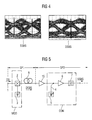
- Fig. 5 shows a composite transmission line.
- a normal ODSB signal is transmitted over a first span SP1 with e.g. 40 km.
- the received signal is amplified by an EDFA span amplifier 15 and transformed the ODSB-OSSB converter CON into an OSSB signal, which is transmitted over a second span SP2.
- This solution is advantageous, when OSSB signals are received from third party lines. Beside the conversion into an OSSB signal a 2R regeneration is performed by the ODSB-OSSB converter: the received signals are amplified and the "1" impulses are shortened.
Landscapes
- Physics & Mathematics (AREA)
- Electromagnetism (AREA)
- Engineering & Computer Science (AREA)
- Computer Networks & Wireless Communication (AREA)
- Signal Processing (AREA)
- Optics & Photonics (AREA)
- Optical Modulation, Optical Deflection, Nonlinear Optics, Optical Demodulation, Optical Logic Elements (AREA)
- Optical Communication System (AREA)
Abstract
Description
- The invention relates to an optical single sideband modulator.
- Optical single sideband modulation OSSB has three important advantages in optical communications compared with double sideband modulation:
- OSSB systems most obvious advantage is the reduction of spectral occupancy and therefore the increased number of transmission channels in a wavelength multiplex signal compared with conventional systems,
- OSSB systems have higher tolerance to chromatic dispersion introduced by the optical transmission fiber,
- OSSB systems allow electrical compensation and electrical precompensation.
- The most common generation of OSSB signals is performed by an optical modulator generating a double sideband signal. The double sideband modulated signal is fed to an optical filter to suppress one sideband.
- This arrangement is expensive and is unable to obtain a good suppression of one sideband without attenuating the optical carrier. Further it has the disadvantage that information can be lost if the filter or laser is detuned.
- It is an object of the invention to provide a low cost optical single sideband modulator without wavelength stability problems.
- According to the present invention the optical single sideband modulator includes an amplitude modulator and a semiconductor optical amplifier [SOA], using a chirp effect to convert an amplitude modulated optical signal into a single sideband signal without the help of a filter for eliminating one of the sidebands.
- The optical single sideband generator can be easily adapted to different bit rates by controlling the power of a modulated optical signal, which is fed to the SOA, or the operating voltage.
- The main advantage of the invention is that the carrier is not suppressed and no information loss according to detuning of a sideband suppression filter results in a loss of information.
-
- Fig. 1 shows the first preferred embodiment of the optical single sideband modulator,
- Fig. 2 shows a second preferred embodiment of a converter,
- Fig. 3 shows a modulated double sideband and a single sideband signal,
- Fig. 4 shows the eye opening for double and single sideband modulation,
- Fig. 5 shows a system with a separate double sideband/single sideband converter.
- Fig. 1 shows a single sideband modulator comprising an optical am modulator MOD/2,3 (amplitude modulation), e.g. Mach-Zehnder modulator, and an ODSB-OSSB converter CON/4,5,6 (optical double sideband - optical single sideband) connected in series.
A binary data signal DS is fed to asignal input 1 of themodulator device 2, which receives a CW (constant wavelength) signal from a laser 3 and outputs an optical amplitude modulated double sideband signal DSBS. This signal is combined with a pump signal PS generated by apump source 5 in a coupler or a filter (wavelength multiplexer) 4 and passed to a signal input of a semiconductor optical amplifier (SOA) 6, which performs the ODSB-OSSB conversion. The pump signal PS is used to maintain the SOA in the saturated region. - The transfer function of the SOA can be described approximately by:

Where Ein is the optical field at the input, Eout is the optical field at the output, α is a parameter known as the linewidth enhancement factor, g is gain of the SOA, which is dependent on the input optical field, L is the length of the SOA, r is the optical confinement factor and αs describes the losses in the waveguide. - [According to Agrawal, G.P. Olsen; N.A. "Self-phase modulation and Spectral Broadening of Optical Pulses in Semiconductor Laser Amplifiers"; IEEE Journal of Quantum Electronics, Vol. 25, No. 11, November 1989]
- According to the formula (1) a phase modulation occurs inside the SOA driven by the input signal. A positive chirp is caused by a "1" to "0" (on → off) transition and a negative chirp is the result of a "0" to "1" (off → on) transition. The negative chirp transfers some power from the upper sideband to the lower sideband and the positive chirp will transfer some power from the lower the upper sideband. Since the power of 1's is higher than the power of 0's and the negative chirp is higher than the positive chirp the power transition to the lower sideband is higher than the power transition to the higher sideband (due to the fact that gain depletion inn a SOA is faster than gain recovery). The result is an optical single sideband signal SSBS.
- The pump signal PS is used to maintain the SOA in the saturation region, otherwise there would be an overshoot in the transitions, especially during 0 to 1 transitions. A band stop filter 7 connected with the output of SOA eliminates the Pump signal.
- The signal SSBS is transmitted - usually after additional amplification; not shown) - from the
converter output 8 over afiber 10 to areceiver - The received signal OSSB is fed to a
signal input 10 of anamplifier 11 and an outputted amplified signal is then converted into the electrical data signal DS by an optical-electrical converter working as ademodulator 12. Of course, chromatic dispersion compensation and polarisation mode dispersion compensation can be used for further improving the signal quality of the received signal. - Fig. 2 shows another preferred embodiment with a second converter CON2 of the single sideband modulator according to the invention. The SOA is pumped backwards over the
coupler 4 by thepump source 5. A pump rejection filter is not necessary. An isolator (or an optical filter) 14, inserted before the signal input of the SOA, keeps the pump signal PS away from themodulator device 2. - Fig. 3 illustrates the difference between a double sideband signal DSBS at the SOA input (top) and the single sideband signal SSBS at the SOA/converter output (below) in the time domain [t] an in the frequency domain [f]. On the left side the vertical axis shows an appropriate output voltage of a demodulator and on the right side the vertical axis shows the output voltage U of a spectral analyser in dB. It can be seen that the upper sideband is highly reduced.
- The improvement of single sideband modulation according to our invention becomes obvious from Fig. 4. On the left side the eye opening is shown for DSB signal DSBS and on the right side for our SSB signal SSBS after 80 km of fiber. Even after 160 km a high quality signal can be attained when SSB modulation according to the invention is used.
- Fig. 5 shows a composite transmission line. A normal ODSB signal is transmitted over a first span SP1 with e.g. 40 km. At end of this span (the beginning of the next span) the received signal is amplified by an EDFA
span amplifier 15 and transformed the ODSB-OSSB converter CON into an OSSB signal, which is transmitted over a second span SP2. This solution is advantageous, when OSSB signals are received from third party lines. Beside the conversion into an OSSB signal a 2R regeneration is performed by the ODSB-OSSB converter: the received signals are amplified and the "1" impulses are shortened.
Claims (4)
- Single sideband modulator,
characterised in that
an optical amplitude modulator (2) and an optical double sideband - optical single sideband converter (CON), comprising a semiconductor optical amplifier (6), are connected in series,
an optical carrier signal (CW) being fed to the optical amplitude modulator (2) and a binary data signal (DS) being fed to its modulation input for generating an optical amplitude modulated double sideband signal (DSBS),
the double sideband signal (DSBS) outputted from the optical amplitude modulator (2) is fed to a signal input of the semiconductor optical amplifier (6) and an optical pump signal (PS) is also fed to the semiconductor optical amplifier (6) to keep it in a saturated region so that an single sideband modulated signal (OSSBS) is generated. - Single sideband modulator according to claim 1,
characterised in that
a coupler or filter (4) is inserted between the optical amplitude modulator (2) and the semiconductor optical amplifier (6), and that the pump signal (PS) is fed to a second input of the coupler or filter (4), where it is combined with the optical double sideband signal (DSBS) and applied to the signal input of the semiconductor optical amplifier (6). - Single sideband modulator according to claim 1,
characterised in that
the coupler or filter (4) is connected to the output of the semiconductor optical amplifier (6) and that the pump signal (PS) is inputted at a second connection point of the coupler or filter (4) and fed backwards to the semiconductor optical amplifier (6). - Single sideband modulator according to claim 1,
characterised in that
the amplitude modulator (MOD) is positioned at the beginning of a transmission span (SP1) and the converter (CON) is positioned at the end of that span (SP1).
Priority Applications (5)
| Application Number | Priority Date | Filing Date | Title |
|---|---|---|---|
| EP05022460A EP1775860B1 (en) | 2005-10-14 | 2005-10-14 | Optical single sideband modulator |
| DE602005007908T DE602005007908D1 (en) | 2005-10-14 | 2005-10-14 | Optical single sideband modulator |
| AT05022460T ATE400099T1 (en) | 2005-10-14 | 2005-10-14 | OPTICAL SINGLE-SIDE BAND MODULATOR |
| CN200610135938XA CN1949689B (en) | 2005-10-14 | 2006-10-13 | Optical single sideband modulator |
| US11/580,767 US20070086788A1 (en) | 2005-10-14 | 2006-10-13 | Optical single sideband modulator |
Applications Claiming Priority (1)
| Application Number | Priority Date | Filing Date | Title |
|---|---|---|---|
| EP05022460A EP1775860B1 (en) | 2005-10-14 | 2005-10-14 | Optical single sideband modulator |
Publications (2)
| Publication Number | Publication Date |
|---|---|
| EP1775860A1 true EP1775860A1 (en) | 2007-04-18 |
| EP1775860B1 EP1775860B1 (en) | 2008-07-02 |
Family
ID=35839027
Family Applications (1)
| Application Number | Title | Priority Date | Filing Date |
|---|---|---|---|
| EP05022460A Expired - Lifetime EP1775860B1 (en) | 2005-10-14 | 2005-10-14 | Optical single sideband modulator |
Country Status (5)
| Country | Link |
|---|---|
| US (1) | US20070086788A1 (en) |
| EP (1) | EP1775860B1 (en) |
| CN (1) | CN1949689B (en) |
| AT (1) | ATE400099T1 (en) |
| DE (1) | DE602005007908D1 (en) |
Families Citing this family (4)
| Publication number | Priority date | Publication date | Assignee | Title |
|---|---|---|---|---|
| US7672598B1 (en) * | 2006-05-24 | 2010-03-02 | The United States Of America As Represented By The Secretary Of The Navy | Carrier signal suppression and extraction system |
| CN101406018B (en) * | 2007-05-24 | 2012-11-21 | 华为技术有限公司 | M-ary phase-shift keying modulation method and system |
| US7881618B2 (en) | 2007-06-07 | 2011-02-01 | Huawei Technologies Co., Ltd. | System and method for m-ary phase-shifting keying modulation |
| US10256934B2 (en) * | 2016-10-11 | 2019-04-09 | Zte Corporation | Chirp managed laser generation for next generation passive optical networks |
Citations (3)
| Publication number | Priority date | Publication date | Assignee | Title |
|---|---|---|---|---|
| US5532857A (en) * | 1994-09-07 | 1996-07-02 | Ael Industries, Inc. | Wide dynamic range optical link using DSSC linearizer |
| US6115162A (en) * | 1995-01-10 | 2000-09-05 | Harris Corporation | Double side band, carrier suppressed modulated coherent fiber optic link |
| US20020171900A1 (en) * | 2001-03-02 | 2002-11-21 | Nec Corporation | Method and circuit for generating single-sideband optical signal |
Family Cites Families (5)
| Publication number | Priority date | Publication date | Assignee | Title |
|---|---|---|---|---|
| US6178036B1 (en) * | 1997-01-14 | 2001-01-23 | California Institute Of Technology | Opto-electronic devices and systems based on brillouin selective sideband amplification |
| GB2321808B (en) * | 1997-01-24 | 1999-03-17 | Plessey Telecomm | Single sideband modulators |
| WO2001052371A1 (en) * | 2000-01-10 | 2001-07-19 | California Institute Of Technology | Optical pulse synthesis using brillouin selective sideband amplification |
| US6959154B1 (en) * | 2000-11-28 | 2005-10-25 | At&T Corp. | Diversity receiver for mitigating the effects of fiber dispersion by separate detection of the two transmitted sidebands |
| EP1684448A1 (en) * | 2005-01-20 | 2006-07-26 | Siemens Aktiengesellschaft | An apparatus and method for generating an optical single sideband signal |
-
2005
- 2005-10-14 EP EP05022460A patent/EP1775860B1/en not_active Expired - Lifetime
- 2005-10-14 AT AT05022460T patent/ATE400099T1/en not_active IP Right Cessation
- 2005-10-14 DE DE602005007908T patent/DE602005007908D1/en not_active Expired - Lifetime
-
2006
- 2006-10-13 CN CN200610135938XA patent/CN1949689B/en not_active Expired - Fee Related
- 2006-10-13 US US11/580,767 patent/US20070086788A1/en not_active Abandoned
Patent Citations (3)
| Publication number | Priority date | Publication date | Assignee | Title |
|---|---|---|---|---|
| US5532857A (en) * | 1994-09-07 | 1996-07-02 | Ael Industries, Inc. | Wide dynamic range optical link using DSSC linearizer |
| US6115162A (en) * | 1995-01-10 | 2000-09-05 | Harris Corporation | Double side band, carrier suppressed modulated coherent fiber optic link |
| US20020171900A1 (en) * | 2001-03-02 | 2002-11-21 | Nec Corporation | Method and circuit for generating single-sideband optical signal |
Non-Patent Citations (1)
| Title |
|---|
| LEE U-S ET AL: "OPTICAL SINGLE SIDEBAND SIGNAL GENERATION USING PHASE MODULATION OF SEMICONDUCTOR OPTICAL AMPLIFIER", IEEE PHOTONICS TECHNOLOGY LETTERS, IEEE SERVICE CENTER, PISCATAWAY, NJ, US, vol. 16, no. 5, May 2004 (2004-05-01), pages 1373 - 1375, XP001212232, ISSN: 1041-1135 * |
Also Published As
| Publication number | Publication date |
|---|---|
| DE602005007908D1 (en) | 2008-08-14 |
| ATE400099T1 (en) | 2008-07-15 |
| CN1949689A (en) | 2007-04-18 |
| EP1775860B1 (en) | 2008-07-02 |
| CN1949689B (en) | 2011-06-08 |
| US20070086788A1 (en) | 2007-04-19 |
Similar Documents
| Publication | Publication Date | Title |
|---|---|---|
| US5793512A (en) | Optical communication system | |
| EP1079552B1 (en) | Method, optical device, and system for optical fiber transmission | |
| US5359450A (en) | Optical transmission system | |
| EP0963065B1 (en) | Control signal superimposing system with Raman amplifier | |
| US9065243B2 (en) | Optical amplifier | |
| US6987607B2 (en) | Optical AND gate and waveform shaping device | |
| EP1841100B1 (en) | Optical signal waveform shaping apparatus | |
| US5508845A (en) | Quasi-soliton communication system | |
| JPH07336297A (en) | System and method for simultaneous compensation of chromatic dispersion and self-phase modulation in an optical fiber | |
| US9584221B2 (en) | Optical transmitter | |
| US20050047797A1 (en) | Duobinary optical transmission device using at least one semiconductor optical amplifier | |
| JP2002023208A (en) | Method and apparatus for waveform shaping signal light | |
| JPH06132895A (en) | Optical power change compensation circuit and optical transmission device | |
| WO1992007430A1 (en) | Quasi-soliton communication system | |
| US6023362A (en) | Optical transmitter having pre-modulation amplification | |
| EP1775860B1 (en) | Optical single sideband modulator | |
| KR20050106073A (en) | Optical transmission system | |
| US20040028355A1 (en) | Method and system for generating short pulse signals | |
| US20040208622A1 (en) | Method and apparatus for signal conditioning of optical signals for fiber-optic transmission | |
| US7412173B2 (en) | Apparatus for generating optical carrier suppressed return-to-zero | |
| US6870665B2 (en) | Pumping source with a number of pumping lasers for the raman amplification of a WDM signal with minimized four-wave mixing | |
| EP0602659A1 (en) | Method of removing frequency modulation from amplitude modulated optical signals | |
| Kavitha et al. | Mixed fiber optical parametric amplifiers for broadband optical communication systems with reduced nonlinear effects | |
| US20260095012A1 (en) | Pump light generation apparatus, optical amplifier and pump light generation method | |
| EP1473856B1 (en) | Duobinary optical transmission apparatus |
Legal Events
| Date | Code | Title | Description |
|---|---|---|---|
| PUAI | Public reference made under article 153(3) epc to a published international application that has entered the european phase |
Free format text: ORIGINAL CODE: 0009012 |
|
| AK | Designated contracting states |
Kind code of ref document: A1 Designated state(s): AT BE BG CH CY CZ DE DK EE ES FI FR GB GR HU IE IS IT LI LT LU LV MC NL PL PT RO SE SI SK TR |
|
| AX | Request for extension of the european patent |
Extension state: AL BA HR MK YU |
|
| RAP1 | Party data changed (applicant data changed or rights of an application transferred) |
Owner name: NOKIA SIEMENS NETWORKS GMBH & CO. KG |
|
| RAP3 | Party data changed (applicant data changed or rights of an application transferred) |
Owner name: NOKIA SIEMENS NETWORKS S.P.A. |
|
| 17P | Request for examination filed |
Effective date: 20071018 |
|
| RAP3 | Party data changed (applicant data changed or rights of an application transferred) |
Owner name: NOKIA SIEMENS NETWORKS GMBH & CO. KG |
|
| AKX | Designation fees paid |
Designated state(s): AT BE BG CH CY CZ DE DK EE ES FI FR GB GR HU IE IS IT LI LT LU LV MC NL PL PT RO SE SI SK TR |
|
| GRAP | Despatch of communication of intention to grant a patent |
Free format text: ORIGINAL CODE: EPIDOSNIGR1 |
|
| GRAS | Grant fee paid |
Free format text: ORIGINAL CODE: EPIDOSNIGR3 |
|
| GRAA | (expected) grant |
Free format text: ORIGINAL CODE: 0009210 |
|
| AK | Designated contracting states |
Kind code of ref document: B1 Designated state(s): AT BE BG CH CY CZ DE DK EE ES FI FR GB GR HU IE IS IT LI LT LU LV MC NL PL PT RO SE SI SK TR |
|
| REG | Reference to a national code |
Ref country code: GB Ref legal event code: FG4D |
|
| REG | Reference to a national code |
Ref country code: CH Ref legal event code: EP |
|
| REF | Corresponds to: |
Ref document number: 602005007908 Country of ref document: DE Date of ref document: 20080814 Kind code of ref document: P |
|
| REG | Reference to a national code |
Ref country code: IE Ref legal event code: FG4D |
|
| PG25 | Lapsed in a contracting state [announced via postgrant information from national office to epo] |
Ref country code: SI Free format text: LAPSE BECAUSE OF FAILURE TO SUBMIT A TRANSLATION OF THE DESCRIPTION OR TO PAY THE FEE WITHIN THE PRESCRIBED TIME-LIMIT Effective date: 20080702 |
|
| PG25 | Lapsed in a contracting state [announced via postgrant information from national office to epo] |
Ref country code: NL Free format text: LAPSE BECAUSE OF FAILURE TO SUBMIT A TRANSLATION OF THE DESCRIPTION OR TO PAY THE FEE WITHIN THE PRESCRIBED TIME-LIMIT Effective date: 20080702 |
|
| NLV1 | Nl: lapsed or annulled due to failure to fulfill the requirements of art. 29p and 29m of the patents act | ||
| PG25 | Lapsed in a contracting state [announced via postgrant information from national office to epo] |
Ref country code: ES Free format text: LAPSE BECAUSE OF FAILURE TO SUBMIT A TRANSLATION OF THE DESCRIPTION OR TO PAY THE FEE WITHIN THE PRESCRIBED TIME-LIMIT Effective date: 20081013 Ref country code: IS Free format text: LAPSE BECAUSE OF FAILURE TO SUBMIT A TRANSLATION OF THE DESCRIPTION OR TO PAY THE FEE WITHIN THE PRESCRIBED TIME-LIMIT Effective date: 20081102 Ref country code: LT Free format text: LAPSE BECAUSE OF FAILURE TO SUBMIT A TRANSLATION OF THE DESCRIPTION OR TO PAY THE FEE WITHIN THE PRESCRIBED TIME-LIMIT Effective date: 20080702 Ref country code: PT Free format text: LAPSE BECAUSE OF FAILURE TO SUBMIT A TRANSLATION OF THE DESCRIPTION OR TO PAY THE FEE WITHIN THE PRESCRIBED TIME-LIMIT Effective date: 20081202 |
|
| PG25 | Lapsed in a contracting state [announced via postgrant information from national office to epo] |
Ref country code: LV Free format text: LAPSE BECAUSE OF FAILURE TO SUBMIT A TRANSLATION OF THE DESCRIPTION OR TO PAY THE FEE WITHIN THE PRESCRIBED TIME-LIMIT Effective date: 20080702 Ref country code: BG Free format text: LAPSE BECAUSE OF FAILURE TO SUBMIT A TRANSLATION OF THE DESCRIPTION OR TO PAY THE FEE WITHIN THE PRESCRIBED TIME-LIMIT Effective date: 20081002 Ref country code: AT Free format text: LAPSE BECAUSE OF FAILURE TO SUBMIT A TRANSLATION OF THE DESCRIPTION OR TO PAY THE FEE WITHIN THE PRESCRIBED TIME-LIMIT Effective date: 20080702 Ref country code: FI Free format text: LAPSE BECAUSE OF FAILURE TO SUBMIT A TRANSLATION OF THE DESCRIPTION OR TO PAY THE FEE WITHIN THE PRESCRIBED TIME-LIMIT Effective date: 20080702 |
|
| PG25 | Lapsed in a contracting state [announced via postgrant information from national office to epo] |
Ref country code: BE Free format text: LAPSE BECAUSE OF FAILURE TO SUBMIT A TRANSLATION OF THE DESCRIPTION OR TO PAY THE FEE WITHIN THE PRESCRIBED TIME-LIMIT Effective date: 20080702 |
|
| PG25 | Lapsed in a contracting state [announced via postgrant information from national office to epo] |
Ref country code: DK Free format text: LAPSE BECAUSE OF FAILURE TO SUBMIT A TRANSLATION OF THE DESCRIPTION OR TO PAY THE FEE WITHIN THE PRESCRIBED TIME-LIMIT Effective date: 20080702 Ref country code: EE Free format text: LAPSE BECAUSE OF FAILURE TO SUBMIT A TRANSLATION OF THE DESCRIPTION OR TO PAY THE FEE WITHIN THE PRESCRIBED TIME-LIMIT Effective date: 20080702 |
|
| PLBE | No opposition filed within time limit |
Free format text: ORIGINAL CODE: 0009261 |
|
| STAA | Information on the status of an ep patent application or granted ep patent |
Free format text: STATUS: NO OPPOSITION FILED WITHIN TIME LIMIT |
|
| PG25 | Lapsed in a contracting state [announced via postgrant information from national office to epo] |
Ref country code: RO Free format text: LAPSE BECAUSE OF FAILURE TO SUBMIT A TRANSLATION OF THE DESCRIPTION OR TO PAY THE FEE WITHIN THE PRESCRIBED TIME-LIMIT Effective date: 20080702 Ref country code: SK Free format text: LAPSE BECAUSE OF FAILURE TO SUBMIT A TRANSLATION OF THE DESCRIPTION OR TO PAY THE FEE WITHIN THE PRESCRIBED TIME-LIMIT Effective date: 20080702 Ref country code: MC Free format text: LAPSE BECAUSE OF NON-PAYMENT OF DUE FEES Effective date: 20081031 Ref country code: CZ Free format text: LAPSE BECAUSE OF FAILURE TO SUBMIT A TRANSLATION OF THE DESCRIPTION OR TO PAY THE FEE WITHIN THE PRESCRIBED TIME-LIMIT Effective date: 20080702 |
|
| 26N | No opposition filed |
Effective date: 20090403 |
|
| REG | Reference to a national code |
Ref country code: IE Ref legal event code: MM4A |
|
| PG25 | Lapsed in a contracting state [announced via postgrant information from national office to epo] |
Ref country code: IT Free format text: LAPSE BECAUSE OF FAILURE TO SUBMIT A TRANSLATION OF THE DESCRIPTION OR TO PAY THE FEE WITHIN THE PRESCRIBED TIME-LIMIT Effective date: 20080702 |
|
| PG25 | Lapsed in a contracting state [announced via postgrant information from national office to epo] |
Ref country code: IE Free format text: LAPSE BECAUSE OF NON-PAYMENT OF DUE FEES Effective date: 20081014 |
|
| PG25 | Lapsed in a contracting state [announced via postgrant information from national office to epo] |
Ref country code: SE Free format text: LAPSE BECAUSE OF FAILURE TO SUBMIT A TRANSLATION OF THE DESCRIPTION OR TO PAY THE FEE WITHIN THE PRESCRIBED TIME-LIMIT Effective date: 20081002 |
|
| PG25 | Lapsed in a contracting state [announced via postgrant information from national office to epo] |
Ref country code: PL Free format text: LAPSE BECAUSE OF FAILURE TO SUBMIT A TRANSLATION OF THE DESCRIPTION OR TO PAY THE FEE WITHIN THE PRESCRIBED TIME-LIMIT Effective date: 20080702 |
|
| REG | Reference to a national code |
Ref country code: CH Ref legal event code: PL |
|
| PG25 | Lapsed in a contracting state [announced via postgrant information from national office to epo] |
Ref country code: CY Free format text: LAPSE BECAUSE OF FAILURE TO SUBMIT A TRANSLATION OF THE DESCRIPTION OR TO PAY THE FEE WITHIN THE PRESCRIBED TIME-LIMIT Effective date: 20080702 Ref country code: LU Free format text: LAPSE BECAUSE OF NON-PAYMENT OF DUE FEES Effective date: 20081014 Ref country code: HU Free format text: LAPSE BECAUSE OF FAILURE TO SUBMIT A TRANSLATION OF THE DESCRIPTION OR TO PAY THE FEE WITHIN THE PRESCRIBED TIME-LIMIT Effective date: 20090103 |
|
| PG25 | Lapsed in a contracting state [announced via postgrant information from national office to epo] |
Ref country code: TR Free format text: LAPSE BECAUSE OF FAILURE TO SUBMIT A TRANSLATION OF THE DESCRIPTION OR TO PAY THE FEE WITHIN THE PRESCRIBED TIME-LIMIT Effective date: 20080702 |
|
| PG25 | Lapsed in a contracting state [announced via postgrant information from national office to epo] |
Ref country code: CH Free format text: LAPSE BECAUSE OF NON-PAYMENT OF DUE FEES Effective date: 20091031 Ref country code: LI Free format text: LAPSE BECAUSE OF NON-PAYMENT OF DUE FEES Effective date: 20091031 Ref country code: GR Free format text: LAPSE BECAUSE OF FAILURE TO SUBMIT A TRANSLATION OF THE DESCRIPTION OR TO PAY THE FEE WITHIN THE PRESCRIBED TIME-LIMIT Effective date: 20081003 |
|
| REG | Reference to a national code |
Ref country code: DE Ref legal event code: R082 Ref document number: 602005007908 Country of ref document: DE Representative=s name: BOEHMERT & BOEHMERT, DE |
|
| REG | Reference to a national code |
Ref country code: DE Ref legal event code: R081 Ref document number: 602005007908 Country of ref document: DE Owner name: XIEON NETWORKS S.A.R.L., LU Free format text: FORMER OWNER: NOKIA SIEMENS NETWORKS GMBH & CO. KG, 81541 MUENCHEN, DE Effective date: 20131106 Ref country code: DE Ref legal event code: R082 Ref document number: 602005007908 Country of ref document: DE Representative=s name: BOEHMERT & BOEHMERT, DE Effective date: 20131106 Ref country code: DE Ref legal event code: R082 Ref document number: 602005007908 Country of ref document: DE Representative=s name: BOEHMERT & BOEHMERT ANWALTSPARTNERSCHAFT MBB -, DE Effective date: 20131106 |
|
| REG | Reference to a national code |
Ref country code: GB Ref legal event code: 732E Free format text: REGISTERED BETWEEN 20131212 AND 20131218 |
|
| REG | Reference to a national code |
Ref country code: GB Ref legal event code: 732E Free format text: REGISTERED BETWEEN 20140130 AND 20140205 |
|
| REG | Reference to a national code |
Ref country code: FR Ref legal event code: GC Effective date: 20140408 Ref country code: FR Ref legal event code: TP Owner name: XIEON NETWORKS S.A.R.L., LU Effective date: 20140408 |
|
| REG | Reference to a national code |
Ref country code: DE Ref legal event code: R079 Ref document number: 602005007908 Country of ref document: DE Free format text: PREVIOUS MAIN CLASS: H04B0010155000 Ipc: H04B0010500000 |
|
| REG | Reference to a national code |
Ref country code: DE Ref legal event code: R079 Ref document number: 602005007908 Country of ref document: DE Free format text: PREVIOUS MAIN CLASS: H04B0010155000 Ipc: H04B0010500000 Effective date: 20141124 |
|
| REG | Reference to a national code |
Ref country code: FR Ref legal event code: GC Effective date: 20150922 Ref country code: FR Ref legal event code: PLFP Year of fee payment: 11 |
|
| PGFP | Annual fee paid to national office [announced via postgrant information from national office to epo] |
Ref country code: GB Payment date: 20151021 Year of fee payment: 11 Ref country code: DE Payment date: 20151022 Year of fee payment: 11 |
|
| PGFP | Annual fee paid to national office [announced via postgrant information from national office to epo] |
Ref country code: FR Payment date: 20151023 Year of fee payment: 11 |
|
| REG | Reference to a national code |
Ref country code: DE Ref legal event code: R119 Ref document number: 602005007908 Country of ref document: DE |
|
| GBPC | Gb: european patent ceased through non-payment of renewal fee |
Effective date: 20161014 |
|
| REG | Reference to a national code |
Ref country code: FR Ref legal event code: ST Effective date: 20170630 |
|
| PG25 | Lapsed in a contracting state [announced via postgrant information from national office to epo] |
Ref country code: DE Free format text: LAPSE BECAUSE OF NON-PAYMENT OF DUE FEES Effective date: 20170503 Ref country code: GB Free format text: LAPSE BECAUSE OF NON-PAYMENT OF DUE FEES Effective date: 20161014 Ref country code: FR Free format text: LAPSE BECAUSE OF NON-PAYMENT OF DUE FEES Effective date: 20161102 |