EP1775764A1 - Semiconductor device and electronic device - Google Patents
Semiconductor device and electronic device Download PDFInfo
- Publication number
- EP1775764A1 EP1775764A1 EP05741482A EP05741482A EP1775764A1 EP 1775764 A1 EP1775764 A1 EP 1775764A1 EP 05741482 A EP05741482 A EP 05741482A EP 05741482 A EP05741482 A EP 05741482A EP 1775764 A1 EP1775764 A1 EP 1775764A1
- Authority
- EP
- European Patent Office
- Prior art keywords
- semiconductor device
- pad
- chip
- wire
- overcurrent protection
- Prior art date
- Legal status (The legal status is an assumption and is not a legal conclusion. Google has not performed a legal analysis and makes no representation as to the accuracy of the status listed.)
- Withdrawn
Links
Images

Classifications
-
- H—ELECTRICITY
- H03—ELECTRONIC CIRCUITRY
- H03K—PULSE TECHNIQUE
- H03K17/00—Electronic switching or gating, i.e. not by contact-making and –breaking
- H03K17/08—Modifications for protecting switching circuit against overcurrent or overvoltage
- H03K17/082—Modifications for protecting switching circuit against overcurrent or overvoltage by feedback from the output to the control circuit
- H03K17/0822—Modifications for protecting switching circuit against overcurrent or overvoltage by feedback from the output to the control circuit in field-effect transistor switches
-
- H—ELECTRICITY
- H10—SEMICONDUCTOR DEVICES; ELECTRIC SOLID-STATE DEVICES NOT OTHERWISE PROVIDED FOR
- H10D—INORGANIC ELECTRIC SEMICONDUCTOR DEVICES
- H10D89/00—Aspects of integrated devices not covered by groups H10D84/00 - H10D88/00
- H10D89/60—Integrated devices comprising arrangements for electrical or thermal protection, e.g. protection circuits against electrostatic discharge [ESD]
Definitions
- the present invention relates to a semiconductor device and an electronic apparatus and it particularly relates to a semiconductor device, where an IC chip is built therein and a pad in the IC chip side is electrically connected with an external terminal of an IC by a bonding wire (hereinafter referred to simply as "wire"), and an electronic apparatus equipped with the semiconductor device.
- a bonding wire hereinafter referred to simply as "wire”
- semiconductor components are incorporated into various electronic equipment.
- the semiconductor components have a wide variety of usages. They are used under severe circumstances depending on the use or they are used under such a condition that they can be easily touched from the outside.
- defects like short-circuiting occur, there are cases where the excessive current as compared to the current normally anticipated flows through the semiconductor components.
- defects such as open and short-circuit is caused in part of the semiconductor components and this malfunction then has adverse effects on the external circuits or apparatus.
- a technique by which to protect the circuit is known where a resistor element is provided to detect the excess current generated at the time when the short-circuiting or the like occurs between the output terminals, etc.
- Patent Document 1 Japanese Patent Application Laid-Open No. Hei05-268724 .
- Patent Document 2 Japanese Patent Application Laid-Open No. Hei06-54865 .
- Patent Document 1 and Patent Document 2 a resistor element that detects the current is used to protect elements inside the semiconductor components.
- the heat is generated by the resistor element itself and the power is consumed thereby as a loss.
- the inventors invented the present invention based on the above recognition and an object thereof is to provide a semiconductor device and an electronic apparatus which alleviate such problems as heat generation and power loss.
- One embodiment of the present invention relates to a semiconductor device.
- This device has an IC chip, the IC chip includes an overcurrent protection circuit, and the overcurrent protection circuit comprises: a first pad connected with an external input terminal; a measuring terminal electrically connected with the first pad via a wire having a predetermined resistive component wherein the measuring terminal is not connected with any of external terminals; a second pad connected to an external output terminal; a switch circuit which turns on and off electric connection between the measuring terminal and the second pad; and a comparator which turns off the switch circuit when difference in potential between the first pad and the measuring terminal exceeds a predetermined value.
- a semiconductor device according to the present invention may further include, besides the comparator, a control circuit which turns on and off the switch circuit according to a predetermined logical control.
- the switch circuit if the voltage potential difference caused in the resistive component of a predetermined wire is greater than an expected value, the switch circuit is turned on so as to protect the semiconductor device from the failure caused by the excess current. As a result, it facilitates suppressing the failure of the external load device from being induced by the failure of the semiconductor device.
- the external resistor which is susceptible to the effect of large variation in connection resistance, wire resistance or the like, and the diffused resistor whose variation in resistance value is large, there is utilized the resistive component that a predetermined wire has. Hence, the problems of heat generation and power loss are alleviated.
- the measuring terminal of the semiconductor device according to the present invention may be a pad. Also, after the IC chip is formed, the wire may be formed external to the IC chip. In this manner, the wire between the first pad and the measuring terminal is formed outside, so that the present characteristics of the IC chip can remain intact and the characteristics are stabilized even after the formation of the wire.
- the external wire may be formed of gold. That is, by the use of gold wiring in place of the aluminum wiring, the problem of corrosion and migration due to prolonged use can be alleviated and therefore high reliability can be realized.
- a semiconductor device according to the present invention is may be such that there are provided a plurality of the overcurrent protection circuits which share the second pad.
- This apparatus comprises: an above-described semiconductor device; and a predetermined load device which is driven by a motor drive circuit, such as an H-bridge circuit, formed by the semiconductor device.
- the load device indicates a device, such as a motor, which operates by utilizing the semiconductor device as a power supply.
- An electronic apparatus may be used for a vehicle and the predetermined value may be determined based on a failure anticipated in the load device in the vehicle.
- the advantages in the above-mentioned electronic apparatus or semiconductor device can also be enjoyed in the electronic apparatus for use in vehicles.
- the vehicles are generally used under severe circumstances or the requested specifications therefor is very demanding, so that it is effective to apply the electronic apparatus of the present invention to the vehicle use.
- a semiconductor device and an electronic apparatus that enhance the long-term reliability and alleviate the problem of heat generation and power loss.
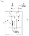
- FIG. 1 is a diagram showing a structure of a first electronic apparatus according to a first embodiment.
- the first electronic apparatus 40 is comprised of a semiconductor device 10 and a load device 31.
- This structure represents a circuit for driving the load device 31 such as a coil or motor, and accordingly it includes a control circuit 22 to achieve a normal operation.
- the semiconductor device 10 has a separate function, in addition to the normal operation, of shutting off the current to countermeasure the overcurrent.
- the load device 31 may suffer closed-circuit failure.
- the semiconductor device 10 supplies the electric power to an external load device 31.
- the semiconductor device 10 has an external input terminal Pi2 and an external output terminal Po2, which are lead terminals, wherein a battery BAT as a power supply is connected with the external input terminal Pi2 and, for example, an input voltage Vi of 4.5 V is supplied thereto. For example, an output voltage Vo of 3.0 V is supplied to the load device 31.
- the semiconductor device 10 has an IC chip that constitutes a series regulator, for example.
- This IC chip 20 includes an overcurrent protection circuit 30, an OR gate S1 and a control circuit 22, the detail of which will be described later.
- the overcurrent protection circuit 30 includes a first pad Pi1, a measuring terminal Pw1, a second pad Po1, an impedance Rp1, a comparator C1, and a PMOS-type transistor Q1.
- the semiconductor device 10 supplies an input voltage Vi to the internal IC chip 20 via an input wire Wi1, and an output voltage Vo is acquired from the IC chip 20 via an output wire Wo1.
- the IC chip 20 includes a first pad Pi1 which receives the input voltage Vi from the power supply, a second pad Po1 which outputs an output voltage Vo for the purpose of performing a control, and a measuring terminal Pw1, electrically connected with the first pad Pi1 by a gold wiring, which is not wire-connected with any external terminals.
- a resistance component, which is generated by the use of the gold wiring, is shown schematically as an impedance Rp1.
- a PMOS-type transistor Q1 is connected between the measuring terminal Pw1 and the second pad Po1.
- a pad is provided to verify, on the wafer level, the value of the impedance Rp1 or the operation of the comparator C1 described later. Note that the measuring terminal Pw1 is not necessary a pad.
- the control circuit 22 outputs "0" corresponding to a low level when the current is to be delivered to the semiconductor device 10 or load device 31. It outputs "1" corresponding to a high level when no current is to be delivered thereto.
- the comparator C1 and the OR gate S1 are provided inside the IC chip 20 and used in combination with the control circuit 22 in order to countermeasure the overcurrent.
- the comparator C1 compares a difference in potential across the impedance Rp1 of a gold wiring provided between the first pad Pi1 and the measuring terminal Pw1 with a predetermined threshold level. And when the potential difference exceeds the predetermined threshold level, it so operates as to turn off the PMOS-type transistor Q1. More specifically, the comparator C1 outputs "1" if the PMOS-type transistor Q1 is to be turned off, whereas it outputs "0" if it is to be turned on. Note that a structure may be such that the threshold level is determined by a user depending on the usage environment, required specifications or the like.
- the threshold level may have a value determined on the assumption that there are various kinds of failures. For example, if the load device 31 such as a coil installed in a vehicle malfunctions due to short-circuiting, the aforementioned threshold level will be determined depending on how much of it suffers short-circuit. If it is assumed that the entire parts suffer short-circuit, the resistance value will drop extremely fast and, as a result thereof, the value of current flowing to the semiconductor device 10 will be very large. Thus, for example, if the maximum value of current which is expected to normally flow is 1 A (ampere), the potential difference which is calculated from 3 A (ampere), namely three times 1 A, may be determined as the threshold level.
- the resistance value of the load device 31 will drop slightly and, as a result thereof, the value of current flowing to the semiconductor device 10 will be slightly larger.
- the maximum value of current which is expected to normally flow is 1 A (ampere)
- the potential difference which is calculated from 1.5 A (ampere), namely 1.5 times 1 A may be determined as the threshold level, which is stricter than the above example.
- the OR gate S1 performs OR-operation on the output signal from the comparator C1 and the output signal from the control circuit 22, and outputs the result to the PMOS-type transistor Q1. Since the output of the comparator C1 is "0", this does not affect the normal operation of the control circuit 22 unless an overcurrent is detected. If, however, the overcurrent occurs, the potential difference across the impedance Rp1 on the gold wire will be larger than a predetermined threshold level and the output of the comparator C1 will be "1". Hence, the output of the control circuit 22 will be ignored and the PMOS-type transistor Q1 will be forcibly turned off.
- the semiconductor device 10 can be protected against the failure due to the overcurrent. Further, the structure can suppress the failure of the external load device 31 from being induced by the failure of the semiconductor device 10. Particularly in the case of the first electronic apparatus 40 used for a vehicle, the vehicles are generally used under severe circumstances or the requested specifications therefor is very demanding, so that it is further effective.
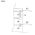
- FIG. 2 is an exterior view showing a state in which the first pad Pi1 and the measuring terminal Pw1 are electrically connected to each other by a gold wire Lg. After the IC chip 20 has been formed, the gold wire Lg is externally formed on the IC chip 20.
- the components equivalent to those in FIG. 1 will be given the same reference numerals and the explanation thereof will be omitted where appropriate.
- the length and width thereof are adjusted, so that the value of the impedance Rp1 can be adjusted to a desired value.
- the impedance by the gold wire Lg is utilized, so that the problem of heat generation and power loss can be alleviated; and the gold wire Lg is utilized instead of the aluminum wire, so that the problem of corrosion and migration due to prolonged use can be alleviated; hence, high reliability can be realized.
- the gold wire Lg between the first pad Pi1 and the measuring terminal Pw1 is formed externally on the IC chip 20, so that it can be formed while the present characteristics of the IC chip 20 is kept intact.
- the designing can be done by still using the existing characteristics.
- FIG. 3 shows a structure of a second electronic apparatus 50 according to a second embodiment.
- This second electronic apparatus 50 is an output stage of a motor driver.
- the components equivalent to those in the first embodiment are given the same reference numerals and the explanation thereof will be omitted as appropriate.
- What the present embodiment differs from the first embodiment is that there are four transistors, and an H-bridge circuit is constituted by using these.
- the arrangement of the first PMOS-type transistor Q1 is the same as that in the first embodiment.
- a first overcurrent protection circuit 30a having the PMOS-type transistor Q1 and a second overcurrent protection circuit 30b having an NMOS-type transistor Q2 are electrically connected so that the drains thereof are commonly used.
- the second overcurrent protection circuit 30b can use commonly a second pad Po1 in the first overcurrent protection circuit 30a, and controls a load device 31, namely the voltage applied to one end of a coil, via an external output terminal Po2 which is wire-connected with a second pad Po1.
- the H-bridge circuit can be structured by further combining, as shown in the Figure, two pairs of circuits constituted by combining the first overcurrent protection circuit 30a and the second overcurrent protection circuit 30b as above.
- One of the above-described two pairs of circuits includes a third overcurrent protection circuit 30c and a fourth overcurrent protection circuit 30d.
- the configurations of the third overcurrent protection circuit 30c and the fourth overcurrent protection circuit 30d are similar to those of the first overcurrent protection circuit 30a and the second overcurrent protection circuit 30b, respectively.
- the signal from a comparator C1 in the first overcurrent protection circuit 30a is inputted to an OR gate S1, whereas the signal from a comparator C2 in the second overcurrent protection circuit 30b is inverted, en route, by an inverting circuit 24 and then inputted to an AND gate S2.
- the signal from a comparator C3 in the third overcurrent protection circuit 30c is inputted to an OR gate S3, whereas the signal from a comparator C4 in the fourth overcurrent protection circuit 30d is inverted by an inverting circuit 24 before it is inputted to an AND gate S4.
- the signal from the control circuit 22 is inputted to the OR gate S1, the AND gate S2, the OR gate S3 and the AND gate S4.
- the first pad Po3, a measuring terminal Pw2, an impedance Rp2 of a gold wire, an output wire Wo2 and an external output terminal Po4 in the second overcurrent protection circuit 30b correspond respectively to the first pad Pi1, the measuring terminal Pw1, the impedance Rp1 of the gold wire, the input wire Wi1 and the external input terminal Pi2 in the first overcurrent protection circuit 30a.
- the current flows to the first pad Pi1 from the external input terminal Pi2 via the input wire Wi in the first overcurrent protection circuit 30a, whereas the current flows to the external output terminal Po4 sequentially in the order of the external output terminal Po2, the second pad Po1, the first pad Po3 and the output wire Wo2 in the second overcurrent protection circuit 30b.
- An AND gate S2 performs an AND operation on the output signal from the comparator C2 and the output signal from the control circuit 22, and outputs the result to the NMOS-type transistor Q2.
- the output of the comparator C2, which is normally "0" is inverted, en route, to "1" by an inverting circuit 24 and inputted to the AND gate S2. This does not affect the normal operation of the control circuit 22 unless an overcurrent is detected.
- the fourth overcurrent protection circuit 30d operates the same way as the second overcurrent protection circuit 30b.
- the comparator C1 can possibly turn off the PMOS-type transistor Q1 in the first overcurrent protection circuit 30a and the comparator C2 can possibly turn off the NMOS-type transistor Q2 in the second overcurrent protection circuit 30b. And the overcurrent can be shut off in any path in an H-bridge circuit configured by those circuits.
- the second electronic apparatus 50 for use in a vehicle, having an H-bridge circuit often delivers a certain degree of current to the load device 31 and a concept of shutting off the overcurrent is required. In the light of this, it is more effective to combine four of overcurrent protection circuits 30, for shutting off the overcurrent, in the first embodiment, and the second electronic apparatus 50 can enjoy the same advantage as with the first embodiment.
- an NMOS-type transistor may be used though the PMOS-type transistor is used in the first embodiment.
- a PMOS-type transistor is used for the first overcurrent protection circuit 30a and an NMOS-type transistor is used for the second overcurrent protection circuit 30b.
- an NMOS-type transistor may be used for the first overcurrent protection circuit 30a and a PMOS-type transistor may be used for the second overcurrent protection circuit 30b.
- the PMOS-type transistor may be used for the both.
- the NMOS-type transistor may be used for the both.
- MOS transistors are used in the embodiments, it goes without saying that the transistor may be of a bipolar type.
- the electronic apparatus may be equipped with other regulators such as a switching regulator and a charge-pump type regulator. Also, it may be a motor driver circuit that derives a three-phase motor.
- the semiconductor device may be one implementing a flip chip that achieves the densification.
- the electronic equipment such as a camera or a mobile phone that demands further downsizing and more sophisticated features is equipped with aforementioned flip-flop, the same effects described as in the first and the second embodiment can be enjoyed.
- a semiconductor device and an electronic apparatus which enhance the long-term reliability and alleviate the problems of heat generation and power loss.
Landscapes
- Semiconductor Integrated Circuits (AREA)
- Electronic Switches (AREA)
- Emergency Protection Circuit Devices (AREA)
Abstract
In a semiconductor device (10), a problem of heat generation and power loss is alleviated, and the semiconductor device (10) is protected against the failure due to the overcurrent. The semiconductor device (10) includes an IC chip (20) having a large-current output. In the IC chip a measuring terminal (Pw1) is electrically connected with a first pad (Pi1) via a gold wire. A potential difference generated by the impedance (Rp1) of the gold wire is compared with a predetermined value. When the potential difference exceeds the predetermined threshold level, the semiconductor devices operates to turn off a PMOS-type transistor (Q1).
Description
- The present invention relates to a semiconductor device and an electronic apparatus and it particularly relates to a semiconductor device, where an IC chip is built therein and a pad in the IC chip side is electrically connected with an external terminal of an IC by a bonding wire (hereinafter referred to simply as "wire"), and an electronic apparatus equipped with the semiconductor device.
- Presently, many semiconductor components are incorporated into various electronic equipment. The semiconductor components have a wide variety of usages. They are used under severe circumstances depending on the use or they are used under such a condition that they can be easily touched from the outside. In such a case, for example, when defects like short-circuiting occur, there are cases where the excessive current as compared to the current normally anticipated flows through the semiconductor components. In such a case, it is possible that defects such as open and short-circuit is caused in part of the semiconductor components and this malfunction then has adverse effects on the external circuits or apparatus. In order to resolve this problem, a technique by which to protect the circuit is known where a resistor element is provided to detect the excess current generated at the time when the short-circuiting or the like occurs between the output terminals, etc. and the load or between the power supply and the ground (
Patent Documents 1 and 2).
[Patent Document 1]
Japanese Patent Application Laid-Open No. Hei05-268724
[Patent Document 2]
Japanese Patent Application Laid-Open No. Hei06-54865 - According to
Patent Document 1 andPatent Document 2, a resistor element that detects the current is used to protect elements inside the semiconductor components. However, as a natural consequence thereof, there is a problem where the heat is generated by the resistor element itself and the power is consumed thereby as a loss. - The inventors invented the present invention based on the above recognition and an object thereof is to provide a semiconductor device and an electronic apparatus which alleviate such problems as heat generation and power loss.
- One embodiment of the present invention relates to a semiconductor device. This device has an IC chip, the IC chip includes an overcurrent protection circuit, and the overcurrent protection circuit comprises: a first pad connected with an external input terminal; a measuring terminal electrically connected with the first pad via a wire having a predetermined resistive component wherein the measuring terminal is not connected with any of external terminals; a second pad connected to an external output terminal; a switch circuit which turns on and off electric connection between the measuring terminal and the second pad; and a comparator which turns off the switch circuit when difference in potential between the first pad and the measuring terminal exceeds a predetermined value. A semiconductor device according to the present invention may further include, besides the comparator, a control circuit which turns on and off the switch circuit according to a predetermined logical control.
- According to this embodiment, if the voltage potential difference caused in the resistive component of a predetermined wire is greater than an expected value, the switch circuit is turned on so as to protect the semiconductor device from the failure caused by the excess current. As a result, it facilitates suppressing the failure of the external load device from being induced by the failure of the semiconductor device. Instead of the external resistor, which is susceptible to the effect of large variation in connection resistance, wire resistance or the like, and the diffused resistor whose variation in resistance value is large, there is utilized the resistive component that a predetermined wire has. Hence, the problems of heat generation and power loss are alleviated.
- The measuring terminal of the semiconductor device according to the present invention may be a pad. Also, after the IC chip is formed, the wire may be formed external to the IC chip. In this manner, the wire between the first pad and the measuring terminal is formed outside, so that the present characteristics of the IC chip can remain intact and the characteristics are stabilized even after the formation of the wire. The external wire may be formed of gold. That is, by the use of gold wiring in place of the aluminum wiring, the problem of corrosion and migration due to prolonged use can be alleviated and therefore high reliability can be realized. A semiconductor device according to the present invention is may be such that there are provided a plurality of the overcurrent protection circuits which share the second pad.
- Another embodiment of the present invention relates to an electronic apparatus. This apparatus comprises: an above-described semiconductor device; and a predetermined load device which is driven by a motor drive circuit, such as an H-bridge circuit, formed by the semiconductor device. Here, the load device indicates a device, such as a motor, which operates by utilizing the semiconductor device as a power supply.
- An electronic apparatus according to the present invention may be used for a vehicle and the predetermined value may be determined based on a failure anticipated in the load device in the vehicle. In that case, the advantages in the above-mentioned electronic apparatus or semiconductor device can also be enjoyed in the electronic apparatus for use in vehicles. The vehicles are generally used under severe circumstances or the requested specifications therefor is very demanding, so that it is effective to apply the electronic apparatus of the present invention to the vehicle use.
- According to the present invention, there can be provided a semiconductor device and an electronic apparatus that enhance the long-term reliability and alleviate the problem of heat generation and power loss.
-
- FIG. 1 is a diagram showing a structure of a first electronic apparatus according to a first embodiment.
- FIG. 2 is an exterior view showing a state in which the first pad Pi1 and the measuring terminal Pw1 are electrically connected to each other by a gold wiring Lg.
- FIG. 3 shows a structure of a second electronic apparatus according to a second embodiment.
- 10 semiconductor device, 20 IC chip, 22 control circuit, 30 overcurrent protection circuit, 31 load device, 40 first electronic apparatus, 50 second electronic apparatus, Pi1, Po3 first pad, Pw1, Pw2 measuring terminal, Po1, second pad, Pi2 external input terminal, Po2, Po4 external output terminal, Wi1, Wo1, Wo2 bonding wire, Lg gold wire, C1, C2, C3, C4 comparator, Q1, Q3 PMOS-type transistor, Q2, Q4 NMOS-type transistor
- FIG. 1 is a diagram showing a structure of a first electronic apparatus according to a first embodiment. The first
electronic apparatus 40 is comprised of asemiconductor device 10 and aload device 31. This structure represents a circuit for driving theload device 31 such as a coil or motor, and accordingly it includes acontrol circuit 22 to achieve a normal operation. On the other hand, thesemiconductor device 10 has a separate function, in addition to the normal operation, of shutting off the current to countermeasure the overcurrent. In a case when thesemiconductor device 10 is used for a vehicle, for example, and is often used under harsh environments such as severe heat and severe coldness, theload device 31 may suffer closed-circuit failure. Also, in a case when an external output terminal Po2 described later is shortcircuited with other output terminals, power supply, grounding and the like, the resistance drops extremely and the overcurrent continues to flow into theload device 31. As a result, theload device 31 generates heat, which in turn may affect the reliability thereof. Thus, it is meaningful to protect thesemiconductor device 10 against the overcurrent generated. - The
semiconductor device 10 supplies the electric power to anexternal load device 31. Thesemiconductor device 10 has an external input terminal Pi2 and an external output terminal Po2, which are lead terminals, wherein a battery BAT as a power supply is connected with the external input terminal Pi2 and, for example, an input voltage Vi of 4.5 V is supplied thereto. For example, an output voltage Vo of 3.0 V is supplied to theload device 31. - The
semiconductor device 10 has an IC chip that constitutes a series regulator, for example. ThisIC chip 20 includes anovercurrent protection circuit 30, an OR gate S1 and acontrol circuit 22, the detail of which will be described later. Theovercurrent protection circuit 30 includes a first pad Pi1, a measuring terminal Pw1, a second pad Po1, an impedance Rp1, a comparator C1, and a PMOS-type transistor Q1. Thesemiconductor device 10 supplies an input voltage Vi to theinternal IC chip 20 via an input wire Wi1, and an output voltage Vo is acquired from theIC chip 20 via an output wire Wo1. - A description will be given hereinabelow of a structure of the
IC chip 20. TheIC chip 20 includes a first pad Pi1 which receives the input voltage Vi from the power supply, a second pad Po1 which outputs an output voltage Vo for the purpose of performing a control, and a measuring terminal Pw1, electrically connected with the first pad Pi1 by a gold wiring, which is not wire-connected with any external terminals. A resistance component, which is generated by the use of the gold wiring, is shown schematically as an impedance Rp1. On the other hand, a PMOS-type transistor Q1 is connected between the measuring terminal Pw1 and the second pad Po1. Here, a pad is provided to verify, on the wafer level, the value of the impedance Rp1 or the operation of the comparator C1 described later. Note that the measuring terminal Pw1 is not necessary a pad. - As a normal operation, the
control circuit 22 outputs "0" corresponding to a low level when the current is to be delivered to thesemiconductor device 10 orload device 31. It outputs "1" corresponding to a high level when no current is to be delivered thereto. In addition to such a normal operation, the comparator C1 and the OR gate S1 are provided inside theIC chip 20 and used in combination with thecontrol circuit 22 in order to countermeasure the overcurrent. - The comparator C1 compares a difference in potential across the impedance Rp1 of a gold wiring provided between the first pad Pi1 and the measuring terminal Pw1 with a predetermined threshold level. And when the potential difference exceeds the predetermined threshold level, it so operates as to turn off the PMOS-type transistor Q1. More specifically, the comparator C1 outputs "1" if the PMOS-type transistor Q1 is to be turned off, whereas it outputs "0" if it is to be turned on. Note that a structure may be such that the threshold level is determined by a user depending on the usage environment, required specifications or the like.
- The threshold level may have a value determined on the assumption that there are various kinds of failures. For example, if the
load device 31 such as a coil installed in a vehicle malfunctions due to short-circuiting, the aforementioned threshold level will be determined depending on how much of it suffers short-circuit. If it is assumed that the entire parts suffer short-circuit, the resistance value will drop extremely fast and, as a result thereof, the value of current flowing to thesemiconductor device 10 will be very large. Thus, for example, if the maximum value of current which is expected to normally flow is 1 A (ampere), the potential difference which is calculated from 3 A (ampere), namely three times 1 A, may be determined as the threshold level. If, otherwise, it is assumed that only a portion of them suffers short-circuit, the resistance value of theload device 31 will drop slightly and, as a result thereof, the value of current flowing to thesemiconductor device 10 will be slightly larger. Thus, for example, if the maximum value of current which is expected to normally flow is 1 A (ampere), the potential difference which is calculated from 1.5 A (ampere), namely 1.5 times 1 A, may be determined as the threshold level, which is stricter than the above example. - The OR gate S1 performs OR-operation on the output signal from the comparator C1 and the output signal from the
control circuit 22, and outputs the result to the PMOS-type transistor Q1. Since the output of the comparator C1 is "0", this does not affect the normal operation of thecontrol circuit 22 unless an overcurrent is detected. If, however, the overcurrent occurs, the potential difference across the impedance Rp1 on the gold wire will be larger than a predetermined threshold level and the output of the comparator C1 will be "1". Hence, the output of thecontrol circuit 22 will be ignored and the PMOS-type transistor Q1 will be forcibly turned off. - According to the above structure, the
semiconductor device 10 can be protected against the failure due to the overcurrent. Further, the structure can suppress the failure of theexternal load device 31 from being induced by the failure of thesemiconductor device 10. Particularly in the case of the firstelectronic apparatus 40 used for a vehicle, the vehicles are generally used under severe circumstances or the requested specifications therefor is very demanding, so that it is further effective. - FIG. 2 is an exterior view showing a state in which the first pad Pi1 and the measuring terminal Pw1 are electrically connected to each other by a gold wire Lg. After the
IC chip 20 has been formed, the gold wire Lg is externally formed on theIC chip 20. Hereinbelow, the components equivalent to those in FIG. 1 will be given the same reference numerals and the explanation thereof will be omitted where appropriate. - As for the gold wire Lg, the length and width thereof are adjusted, so that the value of the impedance Rp1 can be adjusted to a desired value. Instead of using the resistor element or the impedance of the aluminum wiring, the impedance by the gold wire Lg is utilized, so that the problem of heat generation and power loss can be alleviated; and the gold wire Lg is utilized instead of the aluminum wire, so that the problem of corrosion and migration due to prolonged use can be alleviated; hence, high reliability can be realized.
- As shown in the same Figure, the gold wire Lg between the first pad Pi1 and the measuring terminal Pw1 is formed externally on the
IC chip 20, so that it can be formed while the present characteristics of theIC chip 20 is kept intact. Thus, the designing can be done by still using the existing characteristics. - FIG. 3 shows a structure of a second electronic apparatus 50 according to a second embodiment. This second electronic apparatus 50 is an output stage of a motor driver. Hereinbelow, the components equivalent to those in the first embodiment are given the same reference numerals and the explanation thereof will be omitted as appropriate. What the present embodiment differs from the first embodiment is that there are four transistors, and an H-bridge circuit is constituted by using these. The arrangement of the first PMOS-type transistor Q1 is the same as that in the first embodiment. In the IC chip 20 a first
overcurrent protection circuit 30a having the PMOS-type transistor Q1 and a secondovercurrent protection circuit 30b having an NMOS-type transistor Q2 are electrically connected so that the drains thereof are commonly used. As a result, the secondovercurrent protection circuit 30b can use commonly a second pad Po1 in the firstovercurrent protection circuit 30a, and controls aload device 31, namely the voltage applied to one end of a coil, via an external output terminal Po2 which is wire-connected with a second pad Po1. The H-bridge circuit can be structured by further combining, as shown in the Figure, two pairs of circuits constituted by combining the firstovercurrent protection circuit 30a and the secondovercurrent protection circuit 30b as above. One of the above-described two pairs of circuits includes a thirdovercurrent protection circuit 30c and a fourthovercurrent protection circuit 30d. The configurations of the thirdovercurrent protection circuit 30c and the fourthovercurrent protection circuit 30d are similar to those of the firstovercurrent protection circuit 30a and the secondovercurrent protection circuit 30b, respectively. - The signal from a comparator C1 in the first
overcurrent protection circuit 30a is inputted to an OR gate S1, whereas the signal from a comparator C2 in the secondovercurrent protection circuit 30b is inverted, en route, by an invertingcircuit 24 and then inputted to an AND gate S2. Similarly, the signal from a comparator C3 in the thirdovercurrent protection circuit 30c is inputted to an OR gate S3, whereas the signal from a comparator C4 in the fourthovercurrent protection circuit 30d is inverted by an invertingcircuit 24 before it is inputted to an AND gate S4. The signal from thecontrol circuit 22 is inputted to the OR gate S1, the AND gate S2, the OR gate S3 and the AND gate S4. - The first pad Po3, a measuring terminal Pw2, an impedance Rp2 of a gold wire, an output wire Wo2 and an external output terminal Po4 in the second
overcurrent protection circuit 30b correspond respectively to the first pad Pi1, the measuring terminal Pw1, the impedance Rp1 of the gold wire, the input wire Wi1 and the external input terminal Pi2 in the firstovercurrent protection circuit 30a. However, the current flows to the first pad Pi1 from the external input terminal Pi2 via the input wire Wi in the firstovercurrent protection circuit 30a, whereas the current flows to the external output terminal Po4 sequentially in the order of the external output terminal Po2, the second pad Po1, the first pad Po3 and the output wire Wo2 in the secondovercurrent protection circuit 30b. - Hereafter, a description is given of an operation of the second
overcurrent protection circuit 30b in the second electronic apparatus 50 shown in FIG. 3. An AND gate S2 performs an AND operation on the output signal from the comparator C2 and the output signal from thecontrol circuit 22, and outputs the result to the NMOS-type transistor Q2. The output of the comparator C2, which is normally "0", is inverted, en route, to "1" by an invertingcircuit 24 and inputted to the AND gate S2. This does not affect the normal operation of thecontrol circuit 22 unless an overcurrent is detected. If, however, the overcurrent occurs, the potential difference across the impedance Rp1 on the gold wire will be larger than a predetermined threshold level and the output of the comparator C2 will be "1", namely the signal inputted to the AND gate S2 will be "0". Hence, the output of thecontrol circuit 22 will be ignored and the NMOS-type transistor Q2 will be forcibly turned off. The fourthovercurrent protection circuit 30d operates the same way as the secondovercurrent protection circuit 30b. - When an overcurrent occurs, the comparator C1 can possibly turn off the PMOS-type transistor Q1 in the first
overcurrent protection circuit 30a and the comparator C2 can possibly turn off the NMOS-type transistor Q2 in the secondovercurrent protection circuit 30b. And the overcurrent can be shut off in any path in an H-bridge circuit configured by those circuits. - Thereby, the problem can be avoided where the overcurrent continues to flow to the
semiconductor device 10 or the load device 31 (which is a coil here) and then an device fails to operate. In particular, the second electronic apparatus 50, for use in a vehicle, having an H-bridge circuit often delivers a certain degree of current to theload device 31 and a concept of shutting off the overcurrent is required. In the light of this, it is more effective to combine four ofovercurrent protection circuits 30, for shutting off the overcurrent, in the first embodiment, and the second electronic apparatus 50 can enjoy the same advantage as with the first embodiment. - The present invention has been described based on the embodiments. The embodiments are merely exemplary, and it is understood by those skilled in the art that various modifications are possible and that such modifications are also within the scope of the present invention.
- Such modifications will now be described. For example, an NMOS-type transistor may be used though the PMOS-type transistor is used in the first embodiment. In the second embodiment, a PMOS-type transistor is used for the first
overcurrent protection circuit 30a and an NMOS-type transistor is used for the secondovercurrent protection circuit 30b. However, an NMOS-type transistor may be used for the firstovercurrent protection circuit 30a and a PMOS-type transistor may be used for the secondovercurrent protection circuit 30b. The PMOS-type transistor may be used for the both. Or, the NMOS-type transistor may be used for the both. Though MOS transistors are used in the embodiments, it goes without saying that the transistor may be of a bipolar type. - The series regulator and the H-bridge circuit have been described as embodiments. As another modification, the electronic apparatus may be equipped with other regulators such as a switching regulator and a charge-pump type regulator. Also, it may be a motor driver circuit that derives a three-phase motor.
- A description has been given of a semiconductor device where the pad in the IC chip side and the external terminal of the IC is connected by a wire in the first and the second embodiment. However, the semiconductor device may be one implementing a flip chip that achieves the densification. Thereby, if the electronic equipment such as a camera or a mobile phone that demands further downsizing and more sophisticated features is equipped with aforementioned flip-flop, the same effects described as in the first and the second embodiment can be enjoyed.
- According to the present invention, provided are a semiconductor device and an electronic apparatus which enhance the long-term reliability and alleviate the problems of heat generation and power loss.
Claims (8)
- A semiconductor device having an IC chip, said IC chip including:an overcurrent protection circuit which comprises:a first pad connected with an external input terminal;a measuring terminal electrically connected with the first pad via a wire having a predetermined resistive component wherein the measuring terminal is not connected with any of external terminals;a second pad connected to an external output terminal;a switch circuit which turns on and off electric connection between the measuring terminal and the second pad; anda comparator which turns off the switch circuit when difference in potential between the first pad and the measuring terminal exceeds a predetermined value.
- A semiconductor device according to Claim 1, further including, besides the comparator, a control circuit which turns on and off the switch circuit according to a predetermined logical control.
- A semiconductor device according to Claim 1 or 2, wherein the measuring terminal is a pad.
- A semiconductor device according to any of Claim 1 to Claim 3, wherein after the IC chip is formed, the wire is formed external to the IC chip.
- A semiconductor device according to Claim 4, wherein the wire is formed of gold.
- A semiconductor device according to any of Claim 1 to Claim 4, wherein there are provided a plurality of the overcurrent protection circuits which share the second pad.
- An electronic apparatus, comprising:a semiconductor device according to any of Claim 2 to Claim 6; anda predetermined load device which is driven by an H-bridge circuit formed by said semiconductor device.
- An electronic apparatus according to Claim 7, wherein said electronic apparatus is used for a vehicle and the predetermined value is determined based on a failure anticipated in said load device in the vehicle.
Applications Claiming Priority (2)
| Application Number | Priority Date | Filing Date | Title |
|---|---|---|---|
| JP2004163460 | 2004-06-01 | ||
| PCT/JP2005/009391 WO2005119759A1 (en) | 2004-06-01 | 2005-05-23 | Semiconductor device and electronic device |
Publications (1)
| Publication Number | Publication Date |
|---|---|
| EP1775764A1 true EP1775764A1 (en) | 2007-04-18 |
Family
ID=35463126
Family Applications (1)
| Application Number | Title | Priority Date | Filing Date |
|---|---|---|---|
| EP05741482A Withdrawn EP1775764A1 (en) | 2004-06-01 | 2005-05-23 | Semiconductor device and electronic device |
Country Status (6)
| Country | Link |
|---|---|
| US (1) | US20080253047A1 (en) |
| EP (1) | EP1775764A1 (en) |
| JP (1) | JP4833837B2 (en) |
| CN (1) | CN100495684C (en) |
| TW (1) | TW200603381A (en) |
| WO (1) | WO2005119759A1 (en) |
Cited By (3)
| Publication number | Priority date | Publication date | Assignee | Title |
|---|---|---|---|---|
| WO2009114006A1 (en) * | 2008-03-10 | 2009-09-17 | Semiconductor Components Industries, Llc | Method for limiting an un-mirrored current and circuit therefor |
| EP2006998A3 (en) * | 2007-06-20 | 2013-04-17 | Kabushiki Kaisha Tokai-Rika-Denki-Seisakusho | Load drive control circuit |
| CN104168120A (en) * | 2013-05-16 | 2014-11-26 | 弗兰克公司 | Method and apparatus for determining wire resistance |
Families Citing this family (5)
| Publication number | Priority date | Publication date | Assignee | Title |
|---|---|---|---|---|
| CN101557099B (en) * | 2009-05-12 | 2011-09-21 | 中兴通讯股份有限公司 | Module power supply short-circuit protective circuit |
| JP6076630B2 (en) * | 2012-07-11 | 2017-02-08 | ローム株式会社 | Driver circuit |
| CN104502670B (en) * | 2014-12-25 | 2018-02-02 | 小米科技有限责任公司 | Voltage check device, battery and voltage detection method |
| FR3042322B1 (en) * | 2015-10-07 | 2017-11-03 | Continental Automotive France | METHOD FOR LIMITING CURRENT IN "H-BRIDGE" TYPE DEVICES |
| CN116498539B (en) * | 2023-06-27 | 2023-10-20 | 岚图汽车科技有限公司 | Control method, device, equipment and medium for cooling oil pump of oil-cooled motor |
Family Cites Families (7)
| Publication number | Priority date | Publication date | Assignee | Title |
|---|---|---|---|---|
| JPS63252458A (en) * | 1987-04-09 | 1988-10-19 | Nec Corp | semiconductor equipment |
| JP3191618B2 (en) * | 1995-06-13 | 2001-07-23 | 住友電装株式会社 | Power distribution device for automotive wiring harness |
| JP3261974B2 (en) * | 1996-05-20 | 2002-03-04 | 株式会社デンソー | Overcurrent protection circuit |
| JP3424489B2 (en) * | 1997-03-24 | 2003-07-07 | 日産自動車株式会社 | Semiconductor overcurrent detection circuit and its inspection method |
| JP2001053120A (en) * | 1999-08-09 | 2001-02-23 | Sharp Corp | Semiconductor integrated circuit with overcurrent detection function and method of manufacturing the same |
| JP2002208656A (en) * | 2001-01-11 | 2002-07-26 | Mitsubishi Electric Corp | Semiconductor device |
| JP4163019B2 (en) * | 2003-02-06 | 2008-10-08 | シャープ株式会社 | Stabilized power supply device, switching power supply using the same, and electronic equipment |
-
2005
- 2005-05-23 WO PCT/JP2005/009391 patent/WO2005119759A1/en not_active Ceased
- 2005-05-23 JP JP2006514069A patent/JP4833837B2/en not_active Expired - Fee Related
- 2005-05-23 US US11/597,980 patent/US20080253047A1/en not_active Abandoned
- 2005-05-23 EP EP05741482A patent/EP1775764A1/en not_active Withdrawn
- 2005-05-23 CN CNB2005800178751A patent/CN100495684C/en not_active Expired - Fee Related
- 2005-05-31 TW TW094117761A patent/TW200603381A/en not_active IP Right Cessation
Non-Patent Citations (1)
| Title |
|---|
| See references of WO2005119759A1 * |
Cited By (7)
| Publication number | Priority date | Publication date | Assignee | Title |
|---|---|---|---|---|
| EP2006998A3 (en) * | 2007-06-20 | 2013-04-17 | Kabushiki Kaisha Tokai-Rika-Denki-Seisakusho | Load drive control circuit |
| WO2009114006A1 (en) * | 2008-03-10 | 2009-09-17 | Semiconductor Components Industries, Llc | Method for limiting an un-mirrored current and circuit therefor |
| US20110043959A1 (en) * | 2008-03-10 | 2011-02-24 | Paolo Migliavacca | Method for limiting an un-mirrored current and circuit therefor |
| US8737032B2 (en) * | 2008-03-10 | 2014-05-27 | Semiconductor Components Industries, Llc | Method for limiting an un-mirrored current and circuit therefor |
| KR101536104B1 (en) * | 2008-03-10 | 2015-07-13 | 세미컨덕터 콤포넨츠 인더스트리즈 엘엘씨 | Method for limiting an un-mirrored current and circuit therefor |
| CN104168120A (en) * | 2013-05-16 | 2014-11-26 | 弗兰克公司 | Method and apparatus for determining wire resistance |
| CN104168120B (en) * | 2013-05-16 | 2019-08-20 | 弗兰克公司 | Method and apparatus for determining wiring impedance |
Also Published As
| Publication number | Publication date |
|---|---|
| CN100495684C (en) | 2009-06-03 |
| TW200603381A (en) | 2006-01-16 |
| JPWO2005119759A1 (en) | 2008-04-03 |
| CN1961419A (en) | 2007-05-09 |
| WO2005119759A1 (en) | 2005-12-15 |
| JP4833837B2 (en) | 2011-12-07 |
| TWI357654B (en) | 2012-02-01 |
| US20080253047A1 (en) | 2008-10-16 |
Similar Documents
| Publication | Publication Date | Title |
|---|---|---|
| JP5519052B2 (en) | Load drive device | |
| US7538587B2 (en) | Power semiconductor device | |
| EP2071724A1 (en) | Power supply control circuit | |
| US7212036B2 (en) | Driving apparatus of H bridge circuit and protection method of the same | |
| CN101189795A (en) | Power Controllers and Semiconductor Devices | |
| US20130188287A1 (en) | Protection circuit, charge control circuit, and reverse current prevention method employing charge control circuit | |
| JPWO2019193805A1 (en) | Switch drive | |
| US9817412B2 (en) | Protection circuit and control circuit | |
| EP1775764A1 (en) | Semiconductor device and electronic device | |
| KR100594872B1 (en) | Semiconductor device having voltage feedback circuit therein, and electronic apparatus using the same | |
| US20250330095A1 (en) | Dc-dc converter and power supply semiconductor integrated circuit | |
| CN100356568C (en) | Semiconductor device and electronic apparatus capable of detecting open wire using weak current | |
| CN118174260B (en) | Grounding system and control method thereof, chip and chip package | |
| JP4479570B2 (en) | Switching circuit with protection function and protection circuit | |
| JP7518150B2 (en) | Power supply semiconductor integrated circuit and power supply system | |
| US7696707B2 (en) | Semiconductor integrated circuit device | |
| US20240364337A1 (en) | Excessive current protection for bootstrap capacitor charging | |
| KR20070017180A (en) | Semiconductor devices and electronic devices | |
| CN101213652A (en) | Semiconductor integrated circuit device having a plurality of semiconductor chips | |
| JP2025164690A (en) | DC-DC converter and power supply semiconductor integrated circuit | |
| JP6527788B2 (en) | Electromagnetic load drive | |
| US9722457B2 (en) | Semiconductor chip and solar system | |
| TW201407611A (en) | Driving circuit and driving method | |
| JP2008060494A (en) | Semiconductor integrated circuit | |
| CN101341588A (en) | Semiconductor integrated circuit devices and PDP drivers and plasma display panels |
Legal Events
| Date | Code | Title | Description |
|---|---|---|---|
| PUAI | Public reference made under article 153(3) epc to a published international application that has entered the european phase |
Free format text: ORIGINAL CODE: 0009012 |
|
| 17P | Request for examination filed |
Effective date: 20061221 |
|
| AK | Designated contracting states |
Kind code of ref document: A1 Designated state(s): DE FR GB NL |
|
| DAX | Request for extension of the european patent (deleted) | ||
| RBV | Designated contracting states (corrected) |
Designated state(s): DE FR GB NL |
|
| STAA | Information on the status of an ep patent application or granted ep patent |
Free format text: STATUS: THE APPLICATION IS DEEMED TO BE WITHDRAWN |
|
| 18D | Application deemed to be withdrawn |
Effective date: 20090603 |