EP1775755A1 - Euv light source, euv exposure system, and production method for semiconductor device - Google Patents
Euv light source, euv exposure system, and production method for semiconductor device Download PDFInfo
- Publication number
- EP1775755A1 EP1775755A1 EP05755680A EP05755680A EP1775755A1 EP 1775755 A1 EP1775755 A1 EP 1775755A1 EP 05755680 A EP05755680 A EP 05755680A EP 05755680 A EP05755680 A EP 05755680A EP 1775755 A1 EP1775755 A1 EP 1775755A1
- Authority
- EP
- European Patent Office
- Prior art keywords
- target
- light source
- euv light
- melting point
- euv
- Prior art date
- Legal status (The legal status is an assumption and is not a legal conclusion. Google has not performed a legal analysis and makes no representation as to the accuracy of the status listed.)
- Granted
Links
Images




Classifications
-
- G—PHYSICS
- G03—PHOTOGRAPHY; CINEMATOGRAPHY; ANALOGOUS TECHNIQUES USING WAVES OTHER THAN OPTICAL WAVES; ELECTROGRAPHY; HOLOGRAPHY
- G03F—PHOTOMECHANICAL PRODUCTION OF TEXTURED OR PATTERNED SURFACES, e.g. FOR PRINTING, FOR PROCESSING OF SEMICONDUCTOR DEVICES; MATERIALS THEREFOR; ORIGINALS THEREFOR; APPARATUS SPECIALLY ADAPTED THEREFOR
- G03F7/00—Photomechanical, e.g. photolithographic, production of textured or patterned surfaces, e.g. printing surfaces; Materials therefor, e.g. comprising photoresists; Apparatus specially adapted therefor
- G03F7/70—Microphotolithographic exposure; Apparatus therefor
- G03F7/70008—Production of exposure light, i.e. light sources
- G03F7/70033—Production of exposure light, i.e. light sources by plasma extreme ultraviolet [EUV] sources
-
- H—ELECTRICITY
- H05—ELECTRIC TECHNIQUES NOT OTHERWISE PROVIDED FOR
- H05G—X-RAY TECHNIQUE
- H05G2/00—Apparatus or processes specially adapted for producing X-rays, not involving X-ray tubes, e.g. involving generation of a plasma
- H05G2/001—Production of X-ray radiation generated from plasma
- H05G2/003—Production of X-ray radiation generated from plasma the plasma being generated from a material in a liquid or gas state
- H05G2/0035—Production of X-ray radiation generated from plasma the plasma being generated from a material in a liquid or gas state the material containing metals as principal radiation-generating components
Definitions
- the present invention relates to an EUV light source which generates EUV light (extreme ultraviolet light; in the present specification and claims, this refers to light having a wavelength of 13.5 nm), as well as an EUV exposure apparatus using this EUV light source, and a semiconductor device manufacturing method using this EUV exposure apparatus.
- EUV light extreme ultraviolet light
- EUV exposure apparatus using this EUV light source
- semiconductor device manufacturing method using this EUV exposure apparatus.
- the resolution of an exposure apparatus is proportional to the numerical aperture (NA) of the transfer optical system, and is inversely proportional to the wavelength of the light that is used for exposure. Accordingly, as one means of increasing the resolution, there have been attempts to use a short-wavelength EUV light source (also called a "soft X-ray" light source) for exposure and transfer instead of visible light or ultraviolet light.
- NA numerical aperture
- Light sources that are considered to be especially promising as EUV light generating devices used in such exposure and transfer apparatuses are laser plasma EUV light sources (these may be referred to below as “LPP (laser produced plasma)”) and discharge plasma EUV light sources.
- LPP laser produced plasma
- pulsed laser light is focused on a target material inside a vacuum vessel so that this target material is converted into a plasma, and the EUV light that is radiated from this plasma is utilized.
- Such devices have a brightness comparable to that of an undulator, while at the same time being compact.
- EUV light sources using a discharge plasma such as dense plasma focus (DPF) are compact, produce a large amount of EUV light, and are inexpensive.
- DPF dense plasma focus
- these light sources have attracted attention as light sources for EUV exposure apparatuses using EUV light with a wavelength of 13.5 nm.
- IR1 through IR4 are reflective mirrors of an illumination optical system
- PR1 through PR4 are reflective mirrors of a projection optical system.
- W is a wafer
- M is a mask.
- Laser light emitted from a laser light source L is focused on a target S, and X-rays are generated from the target S by the plasma phenomenon. These X-rays are reflected by reflective mirrors C and D, and are incident on the illumination optical system as parallel X-rays. Then, the X-rays are successively reflected by the reflective mirrors IR1 through IR4 of the illumination optical system, and illuminate an illuminated region on the mask M. The X-rays reflected by the pattern formed on the mask M are successively reflected by the reflective mirrors PR1 through PR4 of the projection optical system, so that an image of the pattern is focused on the surface of the wafer W.
- EUV light source utilizing an Xe plasma using Xe gas or liquefied Xe as target substance have been widely researched and developed for EUV light sources with a wavelength of 13.5 nm that is thus used in EUV exposure apparatuses (as well as both laser plasma light sources and discharge plasma light sources).
- the reasons for this are that a relatively high conversion efficiency (ratio of EUV light intensity obtained to input energy) is obtained, and that the problem of debris (scattered particles) tends not to occur since Xe is a gaseous material at ordinary temperatures.
- Sn is known as an element that emits the same 13.5-nm EUV light as Xe. Furthermore, it is also known that if Sn is used, a conversion efficiency higher than that of Xe can be obtained.
- the present invention was devised in light of such circumstances; it is an object of the present invention to provide an EUV light source which makes it possible to obtain a high conversion efficiency by allowing the use of liquid-form Sn, and in which the removal of debris is also easy, as well as an EUV exposure apparatus using this EUV light source, and a semiconductor device manufacturing method using this EUV exposure apparatus.
- the first invention that is used to achieve the object described above is an EUV light source in which a target substance is converted into a plasma, and the EUV light that is emitted in this case is used as a light source, wherein the target is an Sn-Ga (tin-gallium) type alloy in which the atomic % of Sn is 15% or less.
- the target is an Sn-Ga (tin-gallium) type alloy in which the atomic % of Sn is 15% or less.
- the inventor focused on the fact that if the melting point of Sn is lowered as far as possible so that the Sn can be used in a liquid state, the removal of the debris that is generated becomes easy.
- the melting point of Sn itself is 232°C; as was described above, when Sn is used "as is," the removal of debris adhering to the mirror is difficult.
- the Sn can be used in a liquid state; furthermore, if the temperature of the mirror can be raised (to a temperature that does not damage the multilayer film of the mirror), then the adhering debris can be removed as a liquid.
- Sn-Ga titanium-gallium
- Sn-Ga alloys have the special feature of an extremely low melting point of the alloy because of the low melting point of Ga, and the fact that Sn-Ga is a eutectic system.
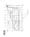
- Figure 1 shows a phase diagram of an Sn-Ga alloy system (below, all phase diagrams are taken from "Collection of Binary Alloy Phase Diagrams," Seizo Nagasaki and Makoto Hirabayashi (eds.), issued by Agne Gijutsu Center).
- the vertical axis indicates temperature.
- the horizontal axis indicates atomic % (at%) on the lower side, and weight % (wt%) on the upper side.
- the melting point of Sn is 232°C
- the melting point of Ga is 29.8°C.
- the uppermost curve connecting the two that the melting point drops as the Sn content ratio decreases, and that the eutectic temperature is 20.5°C at an Sn content of 8 at%.
- This temperature is lower than the melting point of either Sn or Ga.
- the large triangular region that is surrounded by the liquidus line from the melting point of Sn (232°C) to the eutectic point (20.5°C at 8 at% Sn), eutectic line at 20.5°C (horizontal straight line), and vertical curve on the Sn side indicates a two-phase eutectic region of a liquid phase and a compound consisting chiefly of Sn (Sn ratio approximately 93%).
- liquidus line indicates the melting point as an alloy
- a region in which the Sn ratio is 15 at% or less can be used in an Sn-Ga alloy in order to obtain a melting point of 50°C or less.
- a temperature of 50°C was used as a temperature allowing easy heating in the case of use as an EUV light source target.
- the second invention that is used to achieve the object described above is the first invention, wherein the atomic % of Sn in the target is 8% or less.
- the melting point is 29.8°C at the most. Accordingly, even in cases where solid-liquid separation proceeds so that only a Ga solid solution is independently separated, the melting point is 29.8°C at the most. Consequently, a liquid can be formed more easily.
- the third invention that is used to achieve the object described above is the second invention, wherein the atomic % of Sn in the target is the eutectic composition ratio of 8%.
- the target substance can be used in a liquid state even at room temperature, so that the target substance can be supplied as a liquid without any particular heating during target supply as well. Furthermore, since the scattered debris itself is also eutectic, this debris is in a liquid state at room temperature, so that cleaning is also easy. In the case of a eutectic composition, liquid phase ⁇ eutectic fusion and solidification are caused to occur at the single point of the eutectic temperature without any traversal of a region where solid and liquid phases coexist, as though the substance were a simple substance. Accordingly, handling is easy. Furthermore, in the second invention described above, the Sn ratio is highest, so that the conversion efficiency of the EUV light is correspondingly increased.
- the fourth invention that is used to achieve the object described above is an EUV light source in which a target substance is converted into a plasma, and the EUV light that is emitted in this case is used as a light source, wherein the target is an Sn-Ga-In (tin-gallium-indium) ternary alloy containing 15 atomic % or less Sn, 55 to 70 atomic % Ga, and 20 to 30 atomic % In, with the sum of the atomic % of Sn, atomic % of Ga, atomic % of In, and atomic % of impurities being 100%.
- Sn-Ga-In (tin-gallium-indium) ternary alloy containing 15 atomic % or less Sn, 55 to 70 atomic % Ga, and 20 to 30 atomic % In, with the sum of the atomic % of Sn, atomic % of Ga, atomic % of In, and atomic % of impurities being 100%.
- ternary alloys containing Sn Sn-Ga-In (tin-gallium-indium) ternary alloys have a low melting point.
- the melting point can be lowered to 15°C or less by using an alloy with an Sn content of 15 atomic % or less, a Ga content of 55 to 70 atomic %, and an In content of 20 to 30 atomic %.
- the fifth invention that is used to achieve the object described above is the fourth invention, wherein the target is an Sn-Ga-In (tin-gallium-indium) ternary alloy having the eutectic composition ratio and consisting of 62 atomic % Ga, 13 atomic % Sn, and the remainder In and impurities.
- the target is an Sn-Ga-In (tin-gallium-indium) ternary alloy having the eutectic composition ratio and consisting of 62 atomic % Ga, 13 atomic % Sn, and the remainder In and impurities.
- the melting point of the target is 5°C, so that the target is in a completely liquid state at ordinary temperatures.
- the sixth invention that is used to achieve the object described above is an EUV exposure apparatus in which a mask is irradiated with EUV light from an EUV light source via an illumination optical system, and a pattern formed on the mask is exposed and transferred to a reactive substrate such as a wafer by a projection optical system, wherein the EUV light source is the EUV light source of any of the first through fifth inventions.
- the seventh invention that is used to achieve the object described above is a semiconductor device manufacturing method having a process in which a pattern formed on a mask is exposed and transferred to a reactive substrate such as a wafer using the EUV exposure apparatus constituting the sixth invention.
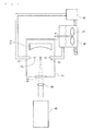
- Figure 3 is a diagram showing an outline of a laser plasma EUV light source constituting a first working configuration of the present invention.
- Sn alloys Sn-Ga type alloy or Sn-Ga-In ternary alloy (hereafter respectively abbreviated to "Sn alloys”) having a composition in the range of the present invention is accommodated inside a heated tank 4.
- a solution agitation mechanism 5 is provided in order to make the temperature of the Sn alloy in the tank 4 uniform, and in order to make the composition of the alloy uniform.
- the solution agitation mechanism 5 is a mechanism that causes vanes to rotate in the liquid.
- the tank 4 is connected to a pressurizing pump 6 by piping, and the Sn alloy pressurized by this pressurizing pump is conducted to a nozzle 1, so that a liquid-form Sn alloy is caused to jet from the tip end of this nozzle 1 disposed inside a vacuum chamber 7.
- the piping extending from the tank 4 to the nozzle 1 via the pressurizing pump 6 is all heated so that the Sn alloy does not solidify en route.
- such a heating mechanism is not absolutely necessary in cases where the melting point of the Sn alloy is sufficiently low.
- the liquid-form Sn alloy that is caused to jet from the nozzle 1 has a spherical shape as a result of surface tension, and forms a target 2.
- the pressurizing pressure, the diameter of the nozzle 1, and the like are set so that a target 2 of fixed dimensions is supplied from the nozzle 1 for a fixed time interval. It is desirable that the target 2 be set so that this target agrees with the amount of target that is converted into plasma and consumed by exactly one pulse of laser irradiation. If the target is too large, the remaining portion of the target that is not converted into plasma will be the cause of debris; accordingly, such an excessively large size is undesirable. Conversely, if the target is too small, the conversion efficiency drops; accordingly, such a small size is likewise undesirable.
- a laser introduction window 10 used for the introduction of laser light is formed in the vacuum chamber 7, and laser light generated by an Nd:YAG laser light source 8 disposed on the outside of the vacuum chamber 7 is focused by a lens 9 and introduced into the vacuum chamber 7.
- the respective parts are disposed so that the target 2 passes through the focal position of the laser, and the target supply and laser pulses are synchronously controlled so that laser pulses are emitted precisely when the target 2 arrives at the focal position.
- the position of the target 2 is monitored by a monitoring mechanism (not shown in the figure), and a light emission trigger is applied to the Nd:YAG laser light source 8 when the target 2 arrives at the focal position of the laser.
- the target 2 that is irradiated by the laser is converted into a plasma, and radiates light that includes EUV light.
- a focusing mirror 11 focuses the EUV light that is generated from the plasma, and conducts this light to the illumination optical system (not shown in the figure).
- the focusing mirror 11 has a reflective surface which has the shape of an ellipsoid of revolution, and the reflective surface of this mirror is coated with a multilayer Mo/Si film. Furthermore, one focal position of the ellipsoid of revolution is the focal position of the laser, i.e., the position where EUV light is generated. Accordingly, the light that is reflected by the focusing mirror 11 is focused at the other focal position, and is then conducted into the illumination optical system.
- the residue of the target 2 that remains without being converted into a plasma is recovered by a target recovery mechanism 3.
- the recovered target residue is returned to the tank 4, and is reutilized after being again heated and melted.
- a backflow prevention mechanism (not shown in the figure) is disposed between the target recovery mechanism 3 and the tank 4, so that the backflow of vapor inside the tank into the vacuum chamber 7 is prevented.
- Figure 5 is a diagram showing an outline of a discharge plasma EUV light source constituting a second working configuration of the present invention.
- An Sn alloy is accommodated inside a heated tank 4.
- a solution agitation mechanism 5 is provided in order to make the temperature of the Sn alloy inside the tank 4 uniform, and in order to make the composition of the alloy uniform.
- the solution agitation mechanism 5 is a mechanism that causes vanes to rotate in the liquid.
- the tank 4 is connected to a pressurizing pump 6 by piping, and the resin pressurized by this pressurizing pump is conducted to a nozzle 1, so that a liquid-form resin caused to jet from the tip end of this nozzle 1 disposed inside a vacuum chamber 7.
- the piping extending from the tank 4 to the nozzle 1 via the pressurizing pump 6 is all heated so that the resin does not solidify en route.
- such a heating mechanism is not absolutely necessary in cases where the melting point of the Sn alloy is sufficiently low.
- the liquid that is caused to jet from the nozzle 1 has a spherical shape as a result of surface tension, and forms a target 2.
- the pressurizing pressure, the diameter of the nozzle 1, and the like are set so that a target 2 of fixed dimensions is supplied from the nozzle 1 for a fixed time interval.
- the target 2 be set so that this target agrees with the amount of target that is converted into plasma and consumed by exactly one pulse of laser irradiation. If the target is too large, the remaining portion of the target that is not converted into plasma will be the cause of debris; accordingly, such an excessively large size is undesirable. Conversely, if the target is too small, the conversion efficiency drops; accordingly, such a small size is likewise undesirable.
- the target 2 that is caused to jet from the nozzle 1 is conducted into the discharge space of a Z-pinch type discharge plasma light source 27.
- This Z-pinch type discharge plasma light source 27 is constructed from a circular disk-form electrode (anode) 21 that has a hole formed therein, an electrode (cathode) 23 that has a similar shape, and a tubular insulator 22 that connects both of these electrodes.
- a high-voltage pulse is applied across the electrode (anode) 21 and electrode (cathode) 23, the substance present in the space between these electrodes is converted into a plasma by the resulting discharge, so that light including EUV light is radiated.
- the respective parts are disposed so that the target 2 passes through the discharge space, and the target supply and high-voltage pulses are synchronously controlled so that a high-voltage pulse is applied precisely when the target 2 arrives at the central position of the discharge space.
- An oscillating mechanism (not shown in the figures) is disposed on the nozzle 1, so that the timing of the jetting of the liquid-form Sn alloy can be controlled by applying an oscillation to the liquid jetting direction of the nozzle 1.
- the oscillation applied to the nozzle 1 and the trigger applied to the high-voltage power supply are controlled so that the synchronization described above is obtained.
- the focusing optical system 26 focuses the EUV light that is generated from the plasma, and conducts this light to the illumination optical system (not shown in the figures).
- the focusing optical system 26 is a Schwarzschild optical system that is constructed from two concentric spherical reflective surfaces 24 and 25; these reflective surfaces are coated with a multilayer Mo/Si film.
- the residue of the target 2 that remains without being converted into a plasma is recovered by a target recovery mechanism 3.
- the recovered target residue is returned to the tank 4, and is reutilized after again being heated and melted.
- a backflow prevention mechanism (not shown in the figures) is disposed between the target recovery mechanism 3 and tank 4, so that the backflow of vapor from the inside of the tank into the vacuum chamber 7 is prevented.
- the positional relationship of the target recovery mechanism 3 and discharge plasma light source 27 is as shown in Figure 6; these parts are disposed so that the central axis of the hole in the electrode 23 and the central axis of the opening part in the target recovery mechanism 3 substantially coincide with each other.
- the target recovery mechanism 3 blocks a portion of the EUV light that is generated by the discharge plasma light source 27. Since the Schwarzschild optical system used in the focusing optical system 26 is an optical system with central blocking, light rays in the vicinity of the optical axis cannot be focused to begin with. In the present working configuration, the target recovery mechanism 3 is disposed as far as possible within the centrally blocked region of the Schwarzschild optical system, so that the loss of EUV light caused by such blockage is minimized.
- a Wolter type optical system can also be used as the focusing optical system 26; however, in this case as well, the optical system is an optical system with central blocking. Accordingly, the loss of EUV light due to blockage can be minimized by a similar disposition.
- the construction of the EUV exposure apparatus constituting a working configuration of the present invention is basically the same as that of the apparatus shown in Figure 8. The only difference is that the laser plasma EUV light source shown in the first working configuration or the discharge plasma EUV light source shown in the second working configuration is used as the EUV light source. Accordingly, a description is omitted.
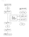
- Figure 7 is a flow chart showing one example of the semiconductor device manufacturing method of the present invention.
- the manufacturing process of this example includes the following main steps:
- the respective steps further consist of several sub-steps.
- the main step that has a definitive effect on the performance of the semiconductor device is the wafer processing step.
- the wafer processing step includes the following respective steps:
- the wafer processing step is repeated a number of times that is equal to the required number of layers, so that semiconductor devices that operate as designed are manufactured.
- the EUV exposure apparatus that constitutes a working configuration of the present invention is used in the lithographic step. Accordingly, the exposure of patterns that have a fine line width can be accomplished, and at the same time, exposure can be performed at a high throughput, so that semiconductor devices can be manufactured with a high efficiency.
- an Sn-Ga alloy was used as the target of the light source of the EUV exposure apparatus.
- a composition of 8 at% Sn and 92 at% Ga was selected as the alloy composition.
- this composition is the eutectic composition in an Sn-Ga alloy, and the melting point is 20.5°C.
- This target is a liquid at room temperature (24°C). Accordingly, this target was placed in a liquid tank, and was caused to jet from a nozzle inside the light source chamber; the target was then converted into a plasma by irradiation with a laser, so that EUV light was emitted.
- the target is an Sn type target containing Sn, and has a high conversion efficiency.
- the proportion of Sn in the target is 8 at%; this amount is a sufficient supply amount for conversion into EUV light. Moreover, the remaining Ga had no deleterious effect on the generation or propagation of EUV light. It was found that the conversion efficiency that was obtained when this target was used was comparable to that obtained when simple Sn was used.
- this target is a liquid
- the used target can easily be recovered as a liquid inside the chamber, and can be passed through pipes and reutilized.
- scattered particles of the target were generated during plasma conversion, and these particles adhered to the facing mirror surface and other members however, since the target was a liquid, there was no firm adhesion to the mirror, so that the particles could easily be rinsed away and removed "as is" during maintenance.
- the liquid target was used without any special operation.
- these parts can be warmed to about 23°C using an appropriately weak heater.
- these particles can easily be melted by heating the mirror to a temperature that is slightly higher than the melting point. Since processing can be performed at a temperature of 25°C or less (at the most), this temperature will cause no thermal damage to either the multilayer film or mirror substrate.
- an Sn-Ga alloy was used as the target of the light source of the EUV exposure apparatus.
- a composition of 5 at% Sn and 95 at% Ga was selected as the alloy composition.
- the melting point of this composition is approximately 25°C.
- This target has separate solid and liquid phases at room temperature (24°C); however, if the target is heated to approximately 30°C, all of the target becomes liquid. Accordingly, the target was stored in a solid or heated liquid state in the target storage part; then, the target was transported from there in a liquid state through heated pipes, and was vaporized inside the light source chamber.
- the target was then converted into a plasma in the vicinity of an electrode that produced a pulse-form high voltage, so that EUV light was generated.
- the target is an Sn type target that contains Sn, and has a high conversion efficiency. Furthermore, the proportion of Sn in the target is 5 at%; this amount is a sufficient supply amount for conversion into EUV light. Moreover, the remaining Ga had no deleterious effect on the generation or propagation of EUV light. It was found that the conversion efficiency that was obtained when this target was used was comparable to that obtained when simple Sn was used.
- the used target can easily be recovered as a liquid inside the chamber by heating the recovery part, and can be transported via heated pipes and reutilized.
- heating by means of a heater is required in order to melt this target; however, the temperature is approximately 30°C at the highest. Furthermore, a melting temperature of approximately 30°C is also sufficient for the removal of debris adhering to the mirror, so that there is no thermal damage to either the multilayer film or mirror substrate.
- an Sn-Ga alloy was used as the target of the light source of the EUV exposure apparatus.
- a composition of 12 at% Sn and 88 at% Ga was selected as the alloy composition.
- the melting point of this composition is approximately 40°C.
- This target has separate solid and liquid phases at room temperature (24°C); however, if the target is heated to approximately 45°C, all of the target becomes liquid. Accordingly, the target was stored in a solid or heated liquid state in the target storage part, and was transported from there in a liquid state via heated pipes, and was caused to jet from a nozzle inside the light source chamber. The target was converted into a plasma by irradiation with a laser, so that EUV light was generated.
- the target is an Sn type target containing Sn, and has a high conversion efficiency. Furthermore, the proportion of Sn in the target is 12 at%; this amount is a sufficient supply amount for conversion into EUV light. Moreover, the remaining Ga had no deleterious effect on the generation or propagation of EUV light. It was found that the conversion efficiency that was obtained when this target was used was comparable to that obtained when simple Sn was used.
- the used target can easily be recovered as a liquid inside the chamber by heating the recovery part, and can be transported via heated pipes and reutilized.
- an Sn-Ga-In alloy was used as the target of the light source of the EUV exposure apparatus.
- a composition of 13 at% Sn, 62 at% Ga and 25 at% In was selected as the alloy composition.
- This composition is the eutectic composition in an Sn-Ga-In ternary alloy, and has a melting point of 5°C.
- This target is a liquid at room temperature (24°C); accordingly, this target was placed inside a liquid tank, vaporized inside the light source chamber, and converted into a plasma in the vicinity of an electrode that generated a pulse-form high voltage, so that EUV light was generated.
- the target is an Sn type target containing Sn, and has a high conversion efficiency.
- the proportion of Sn in the target is 13 at%; this amount is a sufficient supply amount for conversion into EUV light. Moreover, the remaining Ga and In had no deleterious effect on the generation or propagation of EUV light. It was found that the conversion efficiency that was obtained when this target was used was comparable to that obtained when simple Sn was used.
- this target is a liquid
- the used target can easily be recovered as a liquid inside the chamber, and can be passed through pipes and reutilized.
- scattered particles of the target were generated during plasma conversion, and these particles adhered to the facing mirror surface and other members; however, since the target is a liquid, there is no firm adhesion to the mirror, so that the debris can easily be rinsed away and removed "as is" during maintenance.
- the liquid target was used without any special operation.
- the members in cases where there are cooled areas in the vicinity so that there are parts where the temperature is 5°C or less in the flow path of the target, these parts can be warmed to about 10°C using an appropriately weak heater.
- these particles are liquid in the case of ordinary use; accordingly, there is no thermal damage to the mirror substrate, either.
- Sn-Hg titanium-mercury
- Figure 2 A phase diagram of an Sn-Hg (tin-mercury) type alloy is shown as an example in Figure 2.
- the melting point of Ga is 29.8°C, while the melting point of Hg is -39°C
- the liquidus line rises abruptly in the vicinity of an Sn content of 1 to 2 at%, so that the melting point (temperature at which complete melting occurs) rises to 90°C or greater in a composition containing approximately 20 at% Sn.
- an Sn-Hg alloy is also a candidate as an alloy with a low melting point
- the region of complete melting at 50°C or lower is a narrow range of approximately 3 to 4% Sn.
- great care is required in the handling of these alloys.
- the systems listed under (3) and (4) are unsuitable for practical use (the melting point is higher than that of Sn, or substantially the same as that of Sn).
- the systems of (2) have a low melting point in the Na-rich regions, but these systems can contain hardly any Sn.
- the systems of (1) are the most practical sets of alloys; however, since the melting point is 120°C (eutectic point) even in the case of In (indium) which gives the lowest melting point among these systems, it is necessary to set the temperature at 120°C or greater if heating is used as a means of continuous target supply and debris removal. In comparison, it is seen that the eutectic point of 20.5°C shown by an Sn-Ga system is suitable for the target of an EUV light source.
Landscapes
- Physics & Mathematics (AREA)
- Engineering & Computer Science (AREA)
- Plasma & Fusion (AREA)
- Optics & Photonics (AREA)
- General Physics & Mathematics (AREA)
- Exposure And Positioning Against Photoresist Photosensitive Materials (AREA)
- Exposure Of Semiconductors, Excluding Electron Or Ion Beam Exposure (AREA)
- X-Ray Techniques (AREA)
Abstract
Description
- The present invention relates to an EUV light source which generates EUV light (extreme ultraviolet light; in the present specification and claims, this refers to light having a wavelength of 13.5 nm), as well as an EUV exposure apparatus using this EUV light source, and a semiconductor device manufacturing method using this EUV exposure apparatus.
- As the degree of integration of semiconductor integrated circuits has increased, circuit patterns have become finer, and the resolution has become insufficient in the case of conventionally used exposure apparatuses utilizing visible light or ultraviolet light. As is universally known, the resolution of an exposure apparatus is proportional to the numerical aperture (NA) of the transfer optical system, and is inversely proportional to the wavelength of the light that is used for exposure. Accordingly, as one means of increasing the resolution, there have been attempts to use a short-wavelength EUV light source (also called a "soft X-ray" light source) for exposure and transfer instead of visible light or ultraviolet light.
- Light sources that are considered to be especially promising as EUV light generating devices used in such exposure and transfer apparatuses are laser plasma EUV light sources (these may be referred to below as "LPP (laser produced plasma)") and discharge plasma EUV light sources.
- In LPP, pulsed laser light is focused on a target material inside a vacuum vessel so that this target material is converted into a plasma, and the EUV light that is radiated from this plasma is utilized. Such devices have a brightness comparable to that of an undulator, while at the same time being compact.
- Furthermore, EUV light sources using a discharge plasma such as dense plasma focus (DPF) are compact, produce a large amount of EUV light, and are inexpensive. In recent years, these light sources have attracted attention as light sources for EUV exposure apparatuses using EUV light with a wavelength of 13.5 nm.
- An outline of such an EUV exposure apparatus is shown in Figure 8. In this figure, IR1 through IR4 are reflective mirrors of an illumination optical system, and PR1 through PR4 are reflective mirrors of a projection optical system. W is a wafer, and M is a mask.
- Laser light emitted from a laser light source L is focused on a target S, and X-rays are generated from the target S by the plasma phenomenon. These X-rays are reflected by reflective mirrors C and D, and are incident on the illumination optical system as parallel X-rays. Then, the X-rays are successively reflected by the reflective mirrors IR1 through IR4 of the illumination optical system, and illuminate an illuminated region on the mask M. The X-rays reflected by the pattern formed on the mask M are successively reflected by the reflective mirrors PR1 through PR4 of the projection optical system, so that an image of the pattern is focused on the surface of the wafer W.
- EUV light source utilizing an Xe plasma using Xe gas or liquefied Xe as target substance have been widely researched and developed for EUV light sources with a wavelength of 13.5 nm that is thus used in EUV exposure apparatuses (as well as both laser plasma light sources and discharge plasma light sources). The reasons for this are that a relatively high conversion efficiency (ratio of EUV light intensity obtained to input energy) is obtained, and that the problem of debris (scattered particles) tends not to occur since Xe is a gaseous material at ordinary temperatures.
- However, in the case of techniques using Xe gas as a target, there are limits to how far a higher output EUV light source can be obtained, so that there is a demand for the use of other substances. In particular, Sn is known as an element that emits the same 13.5-nm EUV light as Xe. Furthermore, it is also known that if Sn is used, a conversion efficiency higher than that of Xe can be obtained.
- However, since Sn is a metal (solid), the following problems are encountered:
- (1) In the case of a laser plasma light source, a large amount of debris is generated when the solid Sn target is irradiated with the laser. If the Sn is supplied after being heated and converted into a vapor in order to avoid this problem, the density is reduced, so that a sufficiently high conversion efficiency cannot be obtained. Furthermore, solidification occurs in the low-temperature peripheral areas, so that there is a large amount of adhesion in these areas.
- (2) In the case of a discharge plasma light source, it is difficult to supply a material in a solid state to the discharge space (the space where the plasma is generated between the electrodes). If the material is supplied after being heated and vaporized, the material solidifies in the peripheral low-temperature areas, so that large amounts of material adhere in these areas.
- Accordingly, although it is known that Sn is a high-efficiency material, it has been difficult to use Sn "as is" as a target substance in EUV light sources. Consequently, various methods have been tried in order to overcome the demerit of Sn being a solid, which is a problem in cases where Sn is used.
- For example, methods are known in which a water-soluble Sn salt is dissolved in water or another solvent and supplied as a target. In such methods, however, the following problem arises: namely, although water is eliminated by evaporation from the scattered debris following plasma generation, the Sn salt adheres to and contaminates the mirror surface as a solid just as before. Even if an attempt is made to remove the debris adhering to the mirror surface by heating and melting the debris, the heat resistance temperature of the multilayer film on the mirror surface is about 100°C at the most; accordingly, it is not possible to achieve a very high temperature. Furthermore, even if a highly heat-resistant multilayer film that can withstand a temperature of several hundred degrees Celsius is used, there is some concern that the mirror substrate will not be able to withstand this temperature.
- Accordingly, there has been a demand for a supply substance which can be continuously supplied as a target by producing a liquid whose main component is Sn (at room temperature or a lower temperature if possible), and in which scattered debris can also be easily liquefied and removed.
- The present invention was devised in light of such circumstances; it is an object of the present invention to provide an EUV light source which makes it possible to obtain a high conversion efficiency by allowing the use of liquid-form Sn, and in which the removal of debris is also easy, as well as an EUV exposure apparatus using this EUV light source, and a semiconductor device manufacturing method using this EUV exposure apparatus.
- The first invention that is used to achieve the object described above is an EUV light source in which a target substance is converted into a plasma, and the EUV light that is emitted in this case is used as a light source, wherein the target is an Sn-Ga (tin-gallium) type alloy in which the atomic % of Sn is 15% or less.
- As a result of investigating methods using Sn as a target substance in plasma EUV light sources, the inventor focused on the fact that if the melting point of Sn is lowered as far as possible so that the Sn can be used in a liquid state, the removal of the debris that is generated becomes easy. The melting point of Sn itself is 232°C; as was described above, when Sn is used "as is," the removal of debris adhering to the mirror is difficult. However, if the melting point can be lowered by alloying the Sn, the Sn can be used in a liquid state; furthermore, if the temperature of the mirror can be raised (to a temperature that does not damage the multilayer film of the mirror), then the adhering debris can be removed as a liquid.
- The inventor focused on an Sn-Ga (tin-gallium) type alloy as such an Sn alloy. Sn-Ga alloys have the special feature of an extremely low melting point of the alloy because of the low melting point of Ga, and the fact that Sn-Ga is a eutectic system.
- Figure 1 shows a phase diagram of an Sn-Ga alloy system (below, all phase diagrams are taken from "Collection of Binary Alloy Phase Diagrams," Seizo Nagasaki and Makoto Hirabayashi (eds.), issued by Agne Gijutsu Center). The vertical axis indicates temperature. The horizontal axis indicates atomic % (at%) on the lower side, and weight % (wt%) on the upper side. It is seen from this Sn-Ga alloy phase diagram that the melting point of Sn is 232°C, and that the melting point of Ga is 29.8°C. It is seen from the uppermost curve connecting the two (called the liquidus line) that the melting point drops as the Sn content ratio decreases, and that the eutectic temperature is 20.5°C at an Sn content of 8 at%.
- This temperature is lower than the melting point of either Sn or Ga. This is a special feature of eutectic systems, and an Sn-Ga alloy forms a simple eutectic system. Incidentally, the large triangular region that is surrounded by the liquidus line from the melting point of Sn (232°C) to the eutectic point (20.5°C at 8 at% Sn), eutectic line at 20.5°C (horizontal straight line), and vertical curve on the Sn side, indicates a two-phase eutectic region of a liquid phase and a compound consisting chiefly of Sn (Sn ratio approximately 93%).
- In any case, since the liquidus line indicates the melting point as an alloy, it is seen from this phase diagram that a region in which the Sn ratio is 15 at% or less can be used in an Sn-Ga alloy in order to obtain a melting point of 50°C or less. A temperature of 50°C was used as a temperature allowing easy heating in the case of use as an EUV light source target.
- The second invention that is used to achieve the object described above is the first invention, wherein the atomic % of Sn in the target is 8% or less.
- As is seen from Figure 1, in the region where the atomic % of Sn is 8% or less, the melting point is 29.8°C at the most. Accordingly, even in cases where solid-liquid separation proceeds so that only a Ga solid solution is independently separated, the melting point is 29.8°C at the most. Consequently, a liquid can be formed more easily.
- The third invention that is used to achieve the object described above is the second invention, wherein the atomic % of Sn in the target is the eutectic composition ratio of 8%.
- As is seen from Figure 1, when the atomic % of Sn is 8%, the eutectic point is reached, and the eutectic temperature is 20.5°C. Accordingly, the target substance can be used in a liquid state even at room temperature, so that the target substance can be supplied as a liquid without any particular heating during target supply as well. Furthermore, since the scattered debris itself is also eutectic, this debris is in a liquid state at room temperature, so that cleaning is also easy. In the case of a eutectic composition, liquid phase ←→ eutectic fusion and solidification are caused to occur at the single point of the eutectic temperature without any traversal of a region where solid and liquid phases coexist, as though the substance were a simple substance. Accordingly, handling is easy. Furthermore, in the second invention described above, the Sn ratio is highest, so that the conversion efficiency of the EUV light is correspondingly increased.
- The fourth invention that is used to achieve the object described above is an EUV light source in which a target substance is converted into a plasma, and the EUV light that is emitted in this case is used as a light source, wherein the target is an Sn-Ga-In (tin-gallium-indium) ternary alloy containing 15 atomic % or less Sn, 55 to 70 atomic % Ga, and 20 to 30 atomic % In, with the sum of the atomic % of Sn, atomic % of Ga, atomic % of In, and atomic % of impurities being 100%.
- Among ternary alloys containing Sn, Sn-Ga-In (tin-gallium-indium) ternary alloys have a low melting point. In such alloys, the melting point can be lowered to 15°C or less by using an alloy with an Sn content of 15 atomic % or less, a Ga content of 55 to 70 atomic %, and an In content of 20 to 30 atomic %.
- The fifth invention that is used to achieve the object described above is the fourth invention, wherein the target is an Sn-Ga-In (tin-gallium-indium) ternary alloy having the eutectic composition ratio and consisting of 62 atomic % Ga, 13 atomic % Sn, and the remainder In and impurities.
- In this invention, the melting point of the target is 5°C, so that the target is in a completely liquid state at ordinary temperatures.
- The sixth invention that is used to achieve the object described above is an EUV exposure apparatus in which a mask is irradiated with EUV light from an EUV light source via an illumination optical system, and a pattern formed on the mask is exposed and transferred to a reactive substrate such as a wafer by a projection optical system, wherein the EUV light source is the EUV light source of any of the first through fifth inventions.
- In this invention, since a plasma EUV light source having a high conversion efficiency is used, an EUV light source which has a large quantity of light can be realized, so that the throughput can be increased.
- The seventh invention that is used to achieve the object described above is a semiconductor device manufacturing method having a process in which a pattern formed on a mask is exposed and transferred to a reactive substrate such as a wafer using the EUV exposure apparatus constituting the sixth invention.
- In this invention, since an exposure apparatus with a good throughput is used, the production efficiency of semiconductor devices can be increased.
-
- Figure 1 is a phase diagram of an Sn-Ga alloy system.
- Figure 2 is a phase diagram of an Sn-Hg type alloy.
- Figure 3 is a diagram showing an outline of a laser plasma EUV light source constituting a first working configuration of the present invention.
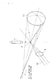
- Figure 4 is a diagram showing the relationship of the respective dispositions of the nozzle that supplies the target, the laser light and the focusing mirror in the working configuration of the present invention shown in Figure 3.
- Figure 5 is a diagram showing an outline of a discharge plasma EUV light source constituting a second working configuration of the present invention.
- Figure 6 is a diagram showing the positional relationship of the target recovery mechanism and the discharge plasma light source in the working configuration of the present invention shown in Figure 5.
- Figure 7 is a flow chart showing one example of the semiconductor device manufacturing method of the present invention.
- Figure 8 is a diagram showing an outline of an EUV exposure apparatus.
- Working configurations of the present invention will be described below using the figures. Figure 3 is a diagram showing an outline of a laser plasma EUV light source constituting a first working configuration of the present invention.
- An Sn-Ga type alloy or Sn-Ga-In ternary alloy (hereafter respectively abbreviated to "Sn alloys") having a composition in the range of the present invention is accommodated inside a
heated tank 4. Asolution agitation mechanism 5 is provided in order to make the temperature of the Sn alloy in thetank 4 uniform, and in order to make the composition of the alloy uniform. In this example, thesolution agitation mechanism 5 is a mechanism that causes vanes to rotate in the liquid. - The
tank 4 is connected to a pressurizingpump 6 by piping, and the Sn alloy pressurized by this pressurizing pump is conducted to anozzle 1, so that a liquid-form Sn alloy is caused to jet from the tip end of thisnozzle 1 disposed inside avacuum chamber 7. The piping extending from thetank 4 to thenozzle 1 via the pressurizingpump 6 is all heated so that the Sn alloy does not solidify en route. However, such a heating mechanism is not absolutely necessary in cases where the melting point of the Sn alloy is sufficiently low. - The liquid-form Sn alloy that is caused to jet from the
nozzle 1 has a spherical shape as a result of surface tension, and forms atarget 2. The pressurizing pressure, the diameter of thenozzle 1, and the like are set so that atarget 2 of fixed dimensions is supplied from thenozzle 1 for a fixed time interval. It is desirable that thetarget 2 be set so that this target agrees with the amount of target that is converted into plasma and consumed by exactly one pulse of laser irradiation. If the target is too large, the remaining portion of the target that is not converted into plasma will be the cause of debris; accordingly, such an excessively large size is undesirable. Conversely, if the target is too small, the conversion efficiency drops; accordingly, such a small size is likewise undesirable. - A
laser introduction window 10 used for the introduction of laser light is formed in thevacuum chamber 7, and laser light generated by an Nd:YAGlaser light source 8 disposed on the outside of thevacuum chamber 7 is focused by alens 9 and introduced into thevacuum chamber 7. - The respective parts are disposed so that the
target 2 passes through the focal position of the laser, and the target supply and laser pulses are synchronously controlled so that laser pulses are emitted precisely when thetarget 2 arrives at the focal position. Specifically, the position of thetarget 2 is monitored by a monitoring mechanism (not shown in the figure), and a light emission trigger is applied to the Nd:YAGlaser light source 8 when thetarget 2 arrives at the focal position of the laser. - The
target 2 that is irradiated by the laser is converted into a plasma, and radiates light that includes EUV light. A focusingmirror 11 focuses the EUV light that is generated from the plasma, and conducts this light to the illumination optical system (not shown in the figure). The focusingmirror 11 has a reflective surface which has the shape of an ellipsoid of revolution, and the reflective surface of this mirror is coated with a multilayer Mo/Si film. Furthermore, one focal position of the ellipsoid of revolution is the focal position of the laser, i.e., the position where EUV light is generated. Accordingly, the light that is reflected by the focusingmirror 11 is focused at the other focal position, and is then conducted into the illumination optical system. - The residue of the
target 2 that remains without being converted into a plasma is recovered by atarget recovery mechanism 3. The recovered target residue is returned to thetank 4, and is reutilized after being again heated and melted. A backflow prevention mechanism (not shown in the figure) is disposed between thetarget recovery mechanism 3 and thetank 4, so that the backflow of vapor inside the tank into thevacuum chamber 7 is prevented. - In Figure 3, it appears that the EUV light that is reflected by the focusing
mirror 11 interferes with thelaser introduction window 10 and the like. In actuality, however, as is shown in Figure 4, the parts are disposed so that the central axis of thenozzle 1 that supplies thetarget 2, the central axis of thelaser light 12, and the axis of the principal rays of the EUV light that is reflected by the focusingmirror 11 are perpendicular to each other. Accordingly, there is no interference of the EUV light with thelaser introduction window 10 or the like. - Figure 5 is a diagram showing an outline of a discharge plasma EUV light source constituting a second working configuration of the present invention. An Sn alloy is accommodated inside a
heated tank 4. Asolution agitation mechanism 5 is provided in order to make the temperature of the Sn alloy inside thetank 4 uniform, and in order to make the composition of the alloy uniform. In this example, thesolution agitation mechanism 5 is a mechanism that causes vanes to rotate in the liquid. - The
tank 4 is connected to a pressurizingpump 6 by piping, and the resin pressurized by this pressurizing pump is conducted to anozzle 1, so that a liquid-form resin caused to jet from the tip end of thisnozzle 1 disposed inside avacuum chamber 7. The piping extending from thetank 4 to thenozzle 1 via the pressurizingpump 6 is all heated so that the resin does not solidify en route. However, such a heating mechanism is not absolutely necessary in cases where the melting point of the Sn alloy is sufficiently low. - The liquid that is caused to jet from the
nozzle 1 has a spherical shape as a result of surface tension, and forms atarget 2. The pressurizing pressure, the diameter of thenozzle 1, and the like are set so that atarget 2 of fixed dimensions is supplied from thenozzle 1 for a fixed time interval. In this working configuration as well, it is desirable that thetarget 2 be set so that this target agrees with the amount of target that is converted into plasma and consumed by exactly one pulse of laser irradiation. If the target is too large, the remaining portion of the target that is not converted into plasma will be the cause of debris; accordingly, such an excessively large size is undesirable. Conversely, if the target is too small, the conversion efficiency drops; accordingly, such a small size is likewise undesirable. - The
target 2 that is caused to jet from thenozzle 1 is conducted into the discharge space of a Z-pinch type dischargeplasma light source 27. This Z-pinch type dischargeplasma light source 27 is constructed from a circular disk-form electrode (anode) 21 that has a hole formed therein, an electrode (cathode) 23 that has a similar shape, and atubular insulator 22 that connects both of these electrodes. When a high-voltage pulse is applied across the electrode (anode) 21 and electrode (cathode) 23, the substance present in the space between these electrodes is converted into a plasma by the resulting discharge, so that light including EUV light is radiated. - The respective parts are disposed so that the
target 2 passes through the discharge space, and the target supply and high-voltage pulses are synchronously controlled so that a high-voltage pulse is applied precisely when thetarget 2 arrives at the central position of the discharge space. - An oscillating mechanism (not shown in the figures) is disposed on the
nozzle 1, so that the timing of the jetting of the liquid-form Sn alloy can be controlled by applying an oscillation to the liquid jetting direction of thenozzle 1. The oscillation applied to thenozzle 1 and the trigger applied to the high-voltage power supply are controlled so that the synchronization described above is obtained. - The focusing
optical system 26 focuses the EUV light that is generated from the plasma, and conducts this light to the illumination optical system (not shown in the figures). The focusingoptical system 26 is a Schwarzschild optical system that is constructed from two concentric sphericalreflective surfaces - The residue of the
target 2 that remains without being converted into a plasma is recovered by atarget recovery mechanism 3. The recovered target residue is returned to thetank 4, and is reutilized after again being heated and melted. A backflow prevention mechanism (not shown in the figures) is disposed between thetarget recovery mechanism 3 andtank 4, so that the backflow of vapor from the inside of the tank into thevacuum chamber 7 is prevented. - The positional relationship of the
target recovery mechanism 3 and dischargeplasma light source 27 is as shown in Figure 6; these parts are disposed so that the central axis of the hole in theelectrode 23 and the central axis of the opening part in thetarget recovery mechanism 3 substantially coincide with each other. - The
target recovery mechanism 3 blocks a portion of the EUV light that is generated by the dischargeplasma light source 27. Since the Schwarzschild optical system used in the focusingoptical system 26 is an optical system with central blocking, light rays in the vicinity of the optical axis cannot be focused to begin with. In the present working configuration, thetarget recovery mechanism 3 is disposed as far as possible within the centrally blocked region of the Schwarzschild optical system, so that the loss of EUV light caused by such blockage is minimized. - Besides a Schwarzschild optical system, a Wolter type optical system can also be used as the focusing
optical system 26; however, in this case as well, the optical system is an optical system with central blocking. Accordingly, the loss of EUV light due to blockage can be minimized by a similar disposition. - The construction of the EUV exposure apparatus constituting a working configuration of the present invention is basically the same as that of the apparatus shown in Figure 8. The only difference is that the laser plasma EUV light source shown in the first working configuration or the discharge plasma EUV light source shown in the second working configuration is used as the EUV light source. Accordingly, a description is omitted.
- A working configuration of the semiconductor device manufacturing method of the present invention will be described below. Figure 7 is a flow chart showing one example of the semiconductor device manufacturing method of the present invention. The manufacturing process of this example includes the following main steps:
- (1) A wafer manufacturing step in which a wafer is manufactured (or a wafer preparation step in which a wafer is prepared);
- (2) A mask manufacturing step in which the mask used in exposure is manufactured (or a mask preparation step in which such a mask is prepared);
- (3) A wafer processing step in which the wafer is subjected to the necessary processing;
- (4) A chip assembly step in which chips formed on the wafer are cut out one at a time, and are made operational; and
- (5) A chip inspection step in which the finished chips are inspected.
- Furthermore, the respective steps further consist of several sub-steps.
- Among these main steps, the main step that has a definitive effect on the performance of the semiconductor device is the wafer processing step. In this step, designed circuit patterns are successively laminated on the wafer, so that numerous chips that operate as memories or MPUs are formed. This wafer processing step includes the following respective steps:
- (1) A thin film formation step (using CVD, sputtering, or the like) in which dielectric thin films forming insulating layers, metal thin films forming wiring parts or electrode parts, or the like, are formed;
- (2) An oxidation step in which such thin film layers or the wafer substrate are oxidized;
- (3) A lithographic step in which a resist pattern is formed using a mask (reticle) in order to achieve selective working of the thin film layers, wafer substrate, or the like;
- (4) An etching step (e.g., using a dry etching technique) which works the thin film layers or substrate in accordance with the resist pattern;
- (5) An ion/impurity injection and diffusion step;
- (6) A resist stripping step; and
- (7) An inspection step in which the worked wafer is further inspected.
- Furthermore, the wafer processing step is repeated a number of times that is equal to the required number of layers, so that semiconductor devices that operate as designed are manufactured.
- In the semiconductor device manufacturing method of the present working configuration, the EUV exposure apparatus that constitutes a working configuration of the present invention is used in the lithographic step. Accordingly, the exposure of patterns that have a fine line width can be accomplished, and at the same time, exposure can be performed at a high throughput, so that semiconductor devices can be manufactured with a high efficiency.
- In the present embodiment, an Sn-Ga alloy was used as the target of the light source of the EUV exposure apparatus. A composition of 8 at% Sn and 92 at% Ga was selected as the alloy composition. As is seen from the Sn-Ga system phase diagram shown in Figure 1, this composition is the eutectic composition in an Sn-Ga alloy, and the melting point is 20.5°C. This target is a liquid at room temperature (24°C). Accordingly, this target was placed in a liquid tank, and was caused to jet from a nozzle inside the light source chamber; the target was then converted into a plasma by irradiation with a laser, so that EUV light was emitted. The target is an Sn type target containing Sn, and has a high conversion efficiency. Furthermore, the proportion of Sn in the target is 8 at%; this amount is a sufficient supply amount for conversion into EUV light. Moreover, the remaining Ga had no deleterious effect on the generation or propagation of EUV light. It was found that the conversion efficiency that was obtained when this target was used was comparable to that obtained when simple Sn was used.
- Since this target is a liquid, the used target can easily be recovered as a liquid inside the chamber, and can be passed through pipes and reutilized.
- Furthermore, with regard to debris, scattered particles of the target (scattered liquid droplets) were generated during plasma conversion, and these particles adhered to the facing mirror surface and other members however, since the target was a liquid, there was no firm adhesion to the mirror, so that the particles could easily be rinsed away and removed "as is" during maintenance.
- In the steps described above, utilizing the fact that the melting point of this target was low, i.e., 20.5°C, the liquid target was used without any special operation. However, depending on the members, in cases where there are cooled areas in the vicinity so that there are parts where the temperature is 20.5°C or less in the flow path of the target, these parts can be warmed to about 23°C using an appropriately weak heater. In cases where there are particles adhering to the mirror as well, these particles can easily be melted by heating the mirror to a temperature that is slightly higher than the melting point. Since processing can be performed at a temperature of 25°C or less (at the most), this temperature will cause no thermal damage to either the multilayer film or mirror substrate.
- In this embodiment, an Sn-Ga alloy was used as the target of the light source of the EUV exposure apparatus. A composition of 5 at% Sn and 95 at% Ga was selected as the alloy composition. As is seen from the Sn-Ga system phase diagram shown in Figure 1, the melting point of this composition is approximately 25°C. This target has separate solid and liquid phases at room temperature (24°C); however, if the target is heated to approximately 30°C, all of the target becomes liquid. Accordingly, the target was stored in a solid or heated liquid state in the target storage part; then, the target was transported from there in a liquid state through heated pipes, and was vaporized inside the light source chamber. The target was then converted into a plasma in the vicinity of an electrode that produced a pulse-form high voltage, so that EUV light was generated. The target is an Sn type target that contains Sn, and has a high conversion efficiency. Furthermore, the proportion of Sn in the target is 5 at%; this amount is a sufficient supply amount for conversion into EUV light. Moreover, the remaining Ga had no deleterious effect on the generation or propagation of EUV light. It was found that the conversion efficiency that was obtained when this target was used was comparable to that obtained when simple Sn was used.
- The used target can easily be recovered as a liquid inside the chamber by heating the recovery part, and can be transported via heated pipes and reutilized.
- Furthermore, with regard to debris, scattered particles of the target (scattered liquid droplets) were generated during plasma conversion, and these particles adhered to the facing mirror surface and other members; however, the debris could all be liquefied by heating the mirror to approximately 30°C during maintenance, so that the debris could easily be rinsed away and removed "as is."
- In the process described above, heating by means of a heater is required in order to melt this target; however, the temperature is approximately 30°C at the highest. Furthermore, a melting temperature of approximately 30°C is also sufficient for the removal of debris adhering to the mirror, so that there is no thermal damage to either the multilayer film or mirror substrate.
- In this embodiment, an Sn-Ga alloy was used as the target of the light source of the EUV exposure apparatus. A composition of 12 at% Sn and 88 at% Ga was selected as the alloy composition. As is seen from the Sn-Ga system phase diagram shown in Figure 1, the melting point of this composition is approximately 40°C. This target has separate solid and liquid phases at room temperature (24°C); however, if the target is heated to approximately 45°C, all of the target becomes liquid. Accordingly, the target was stored in a solid or heated liquid state in the target storage part, and was transported from there in a liquid state via heated pipes, and was caused to jet from a nozzle inside the light source chamber. The target was converted into a plasma by irradiation with a laser, so that EUV light was generated. The target is an Sn type target containing Sn, and has a high conversion efficiency. Furthermore, the proportion of Sn in the target is 12 at%; this amount is a sufficient supply amount for conversion into EUV light. Moreover, the remaining Ga had no deleterious effect on the generation or propagation of EUV light. It was found that the conversion efficiency that was obtained when this target was used was comparable to that obtained when simple Sn was used.
- The used target can easily be recovered as a liquid inside the chamber by heating the recovery part, and can be transported via heated pipes and reutilized.
- Furthermore, with regard to debris, scattered particles of the target (scattered liquid droplets) were generated during plasma conversion, and these particles adhered to the facing mirror surface and other members; however, the debris could all be liquefied by heating the mirror to approximately 45°C during maintenance, so that the debris could easily be rinsed away and removed "as is."
- In the process described above, heating by means of a heater is required in order to melt this target; however, the temperature is approximately 45°C at the highest. Furthermore, a melting temperature of approximately 45°C is also sufficient for the removal of debris adhering to the mirror, so that there is no thermal damage to either the multilayer film or mirror substrate.
- In this embodiment, an Sn-Ga-In alloy was used as the target of the light source of the EUV exposure apparatus. A composition of 13 at% Sn, 62 at% Ga and 25 at% In was selected as the alloy composition. This composition is the eutectic composition in an Sn-Ga-In ternary alloy, and has a melting point of 5°C. This target is a liquid at room temperature (24°C); accordingly, this target was placed inside a liquid tank, vaporized inside the light source chamber, and converted into a plasma in the vicinity of an electrode that generated a pulse-form high voltage, so that EUV light was generated. The target is an Sn type target containing Sn, and has a high conversion efficiency. Furthermore, the proportion of Sn in the target is 13 at%; this amount is a sufficient supply amount for conversion into EUV light. Moreover, the remaining Ga and In had no deleterious effect on the generation or propagation of EUV light. It was found that the conversion efficiency that was obtained when this target was used was comparable to that obtained when simple Sn was used.
- Since this target is a liquid, the used target can easily be recovered as a liquid inside the chamber, and can be passed through pipes and reutilized.
- Furthermore, with regard to debris, scattered particles of the target (scattered liquid droplets) were generated during plasma conversion, and these particles adhered to the facing mirror surface and other members; however, since the target is a liquid, there is no firm adhesion to the mirror, so that the debris can easily be rinsed away and removed "as is" during maintenance.
- Utilizing the fact that the melting point of the target was low, i.e., 5°C, the liquid target was used without any special operation. However, depending on the members, in cases where there are cooled areas in the vicinity so that there are parts where the temperature is 5°C or less in the flow path of the target, these parts can be warmed to about 10°C using an appropriately weak heater. In cases where there are particles adhering to the mirror as well, these particles are liquid in the case of ordinary use; accordingly, there is no thermal damage to the mirror substrate, either.
- The other metals that are used in order to manufacture Sn alloys that have a low melting point are not simply any metals that have a low melting point. A phase diagram of an Sn-Hg (tin-mercury) type alloy is shown as an example in Figure 2. Here, however, in spite of the fact that Hg has a lower melting point than Ga (the melting point of Ga is 29.8°C, while the melting point of Hg is -39°C), the liquidus line rises abruptly in the vicinity of an Sn content of 1 to 2 at%, so that the melting point (temperature at which complete melting occurs) rises to 90°C or greater in a composition containing approximately 20 at% Sn. At temperatures ranging from -34.6°C to the liquidus line, separate solid and liquid regions consisting of a liquid phase that is almost all Hg and a solid solution that is almost all Sn (ε phase, δ phase and y phase) are formed. A temperature that is equal to or greater than the liquidus is required in order to melt all of these phases completely. If Figure 1 and Figure 2 are superimposed, it is seen that the liquidus line in the Sn-Ga phase diagram is lower than the liquidus line in the Sn-Hg phase diagram in the composition range where the Sn content is approximately 2 to 30 at%. Accordingly, although an Sn-Hg alloy is also a candidate as an alloy with a low melting point, the region of complete melting at 50°C or lower is a narrow range of approximately 3 to 4% Sn. Furthermore, since such alloys contain Hg, great care is required in the handling of these alloys.
- For purposes of this discussion, substances other than Hg are cited as examples below.
- (1) Eutectic systems in which the eutectic temperature is less than 200°C:
- Sn-In systems (tin-indium): these are eutectic systems over all, with the lowest melting point being approximately 120°C at the eutectic point (approximately 48 at% Sn). Furthermore, the melting point of In is 157°C.
- Sn-Bi systems (tin-bismuth): these are purely eutectic systems, with the lowest melting point being approximately 139°C at the eutectic point (57 at% Sn). Furthermore, the melting point of Bi is 271°C.
- Sn-Tl systems (tin-thallium) the Sn side is eutectic, with the lowest melting point being 170°C at the eutectic point (approximately 68 at% Sn). Furthermore, the melting point of T1 is 303°C.
- Sn-Cd systems (tin-cadmium): these are eutectic systems, with the lowest melting point being 177°C at the eutectic point (approximately 65 at% Sn). Furthermore, the melting point of Cd is 321°C.
- Sn-Pb systems (tin-lead): these are purely eutectic systems, with the lowest melting point being 183°C at the eutectic point (approximately 74 at% Sn). So-called solder. Furthermore, the melting point of Pb is 328°C.
- Sn-Zn systems (tin-zinc): these are purely eutectic systems, with the lowest melting point being 198°C at the eutectic point (85 at% Sn). Furthermore, the melting point of Zn is 420°C.
- (2) Intermetallic compounds which have a high melting point:
- Sn-Na systems (tin-sodium): the melting point of Sn is 232°C, and the melting point of Na is 97°C; however, the melting point of the alloy may be as high as 578°C. The area in the vicinity of Sn is a eutectic system; the lowest melting point in this vicinity is approximately 215°C at the eutectic point (approximately 95 at% Sn). In the vicinity of Na, the melting point rises abruptly with the admixture of Sn; the melting point at a slight Sn content of approximately 1 at% Sn reaches 200°C. Accordingly, the lowest melting point is approximately 97°C in an alloy containing substantially 100% Na and almost no Sn.
- (3) Alloys in which the eutectic temperature is the lowest melting point, but only the region in the vicinity of 100% Sn is a eutectic system, so that the drop in the melting point is slight.
- Sn-Mg systems (tin-magnesium): eutectic systems with Mg2Sn (intermetallic compound). The lowest melting point is 200°C at the eutectic point (approximately 93 at% Sn). Furthermore, the melting point of Mg is 650°C.
- Sn-Au systems (tin-gold): since only the area in the vicinity of Sn is a eutectic system, the lowest melting point is the eutectic point, but is close to the melting point of Sn at 217°C (approximately 91 at% Sn). Furthermore, the melting point of Au is 1063°C.
- Sn-Ag systems (tin-silver): since only the area in the vicinity of Sn is a eutectic system, the lowest melting point is the eutectic point, but is close to the melting point of Sn at 221°C (approximately 95 at% Sn). Furthermore, the melting point of Ag is 962°C.
- Sn-Cu systems (tin-copper): since only the area in the vicinity of Sn is a eutectic system, the lowest melting point is the eutectic point, but is close to the melting point of Sn at 227°C (approximately 99 at% Sn). Furthermore, the melting point of Cu is 1083°C.
- Sn-Al systems (tin-aluminum): these are purely eutectic systems, but the eutectic point is inclined considerably toward Sn; accordingly, the lowest melting point is the eutectic point, but is substantially the same as the melting point of Sn at 228°C (approximately 98 at% Sn). Furthermore, the melting point of A1 is 660°C.
- Sn-Pt systems (tin-platinum): since only the area in the vicinity of Sn is a eutectic system, the lowest melting point is the eutectic point, but is substantially the same as the melting point of Sn at 228°C (approximately 98 at% Sn). Furthermore, the melting point of Pt is 1769°C.
- Sn-Co systems (tin-cobalt): since only the area in the vicinity of Sn is a eutectic system, the lowest melting point is the eutectic point, but is close to the melting point of Sn at 229°C (approximately 99 at% Sn). Furthermore, the melting point of Co is 1495°C.
- Sn-Y systems (tin-yttrium): since only the area in the vicinity of Sn is a eutectic system, the lowest melting point is the eutectic point, but is close to the melting point of Sn at 229°C (approximately 99 at% Sn). Furthermore, the melting point of Y is 1522°C.
- Sn-Te systems (tin-tellurium): a eutectic system is formed with the intermetallic compound SnTe; however, the eutectic point is substantially the same as that of Sn, so that the lowest melting point is 232°C (99 at% Sn). Furthermore, the melting point of Te is 450°C.
- Sn-Ge systems (tin-germanium): these systems are eutectic systems, but the eutectic point is substantially the same as that of Sn, so that the lowest melting point is 232°C (99.7 at% Sn). Furthermore, the melting point of Ge is 938°C.
- (4) Peritectic systems or the like in which the melting point is caused to rise as a result of the admixture of the other metal (systems in which the lowest melting point is the melting point of Sn).
- Sn-As systems (tin-arsenic), Sn-Fe systems (tin-iron), Sn-Ge systems (tin-germanium), Sn-Mn systems (tin-manganese), Sn-Nb systems (tin-niobium), Sn-Ni systems (tin-nickel), Sn-Pd systems (tin-palladium), Sn-Sb systems (tin-antimony), Sn-Se systems (tin-selenium)
- Among all of the systems in the above list, the systems listed under (3) and (4) are unsuitable for practical use (the melting point is higher than that of Sn, or substantially the same as that of Sn). The systems of (2) have a low melting point in the Na-rich regions, but these systems can contain hardly any Sn. The systems of (1) are the most practical sets of alloys; however, since the melting point is 120°C (eutectic point) even in the case of In (indium) which gives the lowest melting point among these systems, it is necessary to set the temperature at 120°C or greater if heating is used as a means of continuous target supply and debris removal. In comparison, it is seen that the eutectic point of 20.5°C shown by an Sn-Ga system is suitable for the target of an EUV light source.
Claims (9)
- An EUV light source in which a target substance is converted into a plasma, and the EUV light that is emitted in this case is used as a light source, wherein the target is an Sn-Ga (tin-gallium) type alloy in which the atomic % of Sn is 15% or less.
- The EUV light source according to Claim 1, wherein the atomic % of Sn in the target is 8% or less.
- The EUV light source according to Claim 2, wherein the atomic % of Sn in the target is the eutectic composition ratio of 8%.
- An EUV light source in which a target substance is converted into a plasma, and the EUV light that is emitted in this case is used as a light source, wherein the target is an Sn-Ga-In (tin-gallium-indium) ternary alloy containing 15 atomic % or less Sn, 55 to 70 atomic % Ga, and 20 to 30 atomic % In, with the sum of the atomic % of Sn, atomic % of Ga, atomic % of In, and atomic % of impurities being 100%.
- The EUV light source according to Claim 4, wherein the target is an Sn-Ga-In (tin-gallium-indium) ternary alloy having the eutectic composition ratio and consisting of 62 atomic % Ga, 13 atomic % Sn, and the remainder In and impurities.
- An EUV exposure apparatus in which a mask is irradiated with EUV light from an EUV light source via an illumination optical system, and a pattern formed on the mask is exposed and transferred to a reactive substrate such as a wafer by a projection optical system, wherein the EUV light source is the EUV light source according to Claim 1.
- An EUV exposure apparatus in which a mask is irradiated with EUV light from an EUV light source via an illumination optical system, and a pattern formed on the mask is exposed and transferred to a reactive substrate such as a wafer by a projection optical system, wherein the EUV light source is the EUV light source according to Claim 4.
- A semiconductor device manufacturing method having a process in which a pattern formed on a mask is exposed and transferred to a reactive substrate such as a wafer using the EUV exposure apparatus according to Claim 6.
- A semiconductor device manufacturing method having a process in which a pattern formed on a mask is exposed and transferred to a reactive substrate such as a wafer using the EUV exposure apparatus according to Claim 7.
Priority Applications (1)
| Application Number | Priority Date | Filing Date | Title |
|---|---|---|---|
| EP12171328.3A EP2498275B1 (en) | 2004-06-24 | 2005-06-22 | EUV light source, EUV exposure system, and production method for semiconductor device |
Applications Claiming Priority (2)
| Application Number | Priority Date | Filing Date | Title |
|---|---|---|---|
| JP2004186132A JP4337648B2 (en) | 2004-06-24 | 2004-06-24 | EUV LIGHT SOURCE, EUV EXPOSURE APPARATUS, AND METHOD FOR MANUFACTURING SEMICONDUCTOR DEVICE |
| PCT/JP2005/012007 WO2006006408A1 (en) | 2004-06-24 | 2005-06-22 | Euv light source, euv exposure system, and production method for semiconductor device |
Related Child Applications (2)
| Application Number | Title | Priority Date | Filing Date |
|---|---|---|---|
| EP12171328.3A Division EP2498275B1 (en) | 2004-06-24 | 2005-06-22 | EUV light source, EUV exposure system, and production method for semiconductor device |
| EP12171328.3A Division-Into EP2498275B1 (en) | 2004-06-24 | 2005-06-22 | EUV light source, EUV exposure system, and production method for semiconductor device |
Publications (3)
| Publication Number | Publication Date |
|---|---|
| EP1775755A1 true EP1775755A1 (en) | 2007-04-18 |
| EP1775755A4 EP1775755A4 (en) | 2010-03-17 |
| EP1775755B1 EP1775755B1 (en) | 2012-09-26 |
Family
ID=35779920
Family Applications (2)
| Application Number | Title | Priority Date | Filing Date |
|---|---|---|---|
| EP05755680A Expired - Lifetime EP1775755B1 (en) | 2004-06-24 | 2005-06-22 | Euv light source, euv exposure system, and production method for semiconductor device |
| EP12171328.3A Expired - Lifetime EP2498275B1 (en) | 2004-06-24 | 2005-06-22 | EUV light source, EUV exposure system, and production method for semiconductor device |
Family Applications After (1)
| Application Number | Title | Priority Date | Filing Date |
|---|---|---|---|
| EP12171328.3A Expired - Lifetime EP2498275B1 (en) | 2004-06-24 | 2005-06-22 | EUV light source, EUV exposure system, and production method for semiconductor device |
Country Status (6)
| Country | Link |
|---|---|
| US (1) | US7491955B2 (en) |
| EP (2) | EP1775755B1 (en) |
| JP (1) | JP4337648B2 (en) |
| KR (1) | KR101174926B1 (en) |
| CN (1) | CN1973357B (en) |
| WO (1) | WO2006006408A1 (en) |
Cited By (4)
| Publication number | Priority date | Publication date | Assignee | Title |
|---|---|---|---|---|
| US20100025231A1 (en) * | 2007-04-27 | 2010-02-04 | Komatsu Ltd. | Method for cleaning optical element of EUV light source device and optical element cleaning device |
| EP2170021A3 (en) * | 2008-09-25 | 2010-04-28 | ASML Netherlands B.V. | Source module, radiation source and lithographic apparatus |
| WO2013023710A1 (en) * | 2011-08-12 | 2013-02-21 | Asml Netherlands B.V. | Radiation source |
| US8809818B2 (en) | 2007-07-06 | 2014-08-19 | Nikon Corporation | EUV light source, EUV exposure apparatus, and electronic device manufacturing method |
Families Citing this family (28)
| Publication number | Priority date | Publication date | Assignee | Title |
|---|---|---|---|---|
| JP5156193B2 (en) * | 2006-02-01 | 2013-03-06 | ギガフォトン株式会社 | Extreme ultraviolet light source device |
| JP2008053696A (en) * | 2006-07-28 | 2008-03-06 | Ushio Inc | Extreme ultraviolet light source device and extreme ultraviolet light generation method |
| JP5149520B2 (en) * | 2007-03-08 | 2013-02-20 | ギガフォトン株式会社 | Extreme ultraviolet light source device |
| US20080239262A1 (en) * | 2007-03-29 | 2008-10-02 | Asml Netherlands B.V. | Radiation source for generating electromagnetic radiation and method for generating electromagnetic radiation |
| US8493548B2 (en) * | 2007-08-06 | 2013-07-23 | Asml Netherlands B.V. | Lithographic apparatus and device manufacturing method |
| US20090095924A1 (en) * | 2007-10-12 | 2009-04-16 | International Business Machines Corporation | Electrode design for euv discharge plasma source |
| NL1036614A1 (en) * | 2008-03-21 | 2009-09-22 | Asml Netherlands Bv | A target material, a source, an EUV lithographic apparatus and a device manufacturing method using the same. |
| TWI490408B (en) | 2008-04-04 | 2015-07-01 | Brooks Automation Inc | Cryogenic pump employing tin-gallium alloys |
| EP2300879B1 (en) * | 2008-07-18 | 2011-10-12 | Philips Intellectual Property & Standards GmbH | Extreme uv radiation generating device comprising a contamination captor and method of purifying tin in said device |
| JP5426317B2 (en) * | 2008-10-23 | 2014-02-26 | ギガフォトン株式会社 | Extreme ultraviolet light source device |
| JP2010110790A (en) * | 2008-11-06 | 2010-05-20 | Miyachi Technos Corp | Fusing method |
| JP5574470B2 (en) * | 2009-06-12 | 2014-08-20 | 国立大学法人 宮崎大学 | Extreme ultraviolet light source and method for generating extreme ultraviolet light |
| US9265136B2 (en) | 2010-02-19 | 2016-02-16 | Gigaphoton Inc. | System and method for generating extreme ultraviolet light |
| US9113540B2 (en) | 2010-02-19 | 2015-08-18 | Gigaphoton Inc. | System and method for generating extreme ultraviolet light |
| JP5563012B2 (en) * | 2012-04-18 | 2014-07-30 | ギガフォトン株式会社 | Extreme ultraviolet light source device |
| CN103042221B (en) * | 2012-12-14 | 2015-04-15 | 华中科技大学 | High-melting-point material droplet target generating device for extreme ultraviolet light source |
| DE102013212779A1 (en) * | 2013-07-01 | 2014-07-10 | Carl Zeiss Smt Gmbh | Device for cleaning mirror of microlithographic projection exposure apparatus, has feeding device for feeding liquid metallic material to optical active surface of mirror, where metallic material together with target material forms eutectic |
| TWI527085B (en) * | 2013-08-27 | 2016-03-21 | 東芝股份有限公司 | Inspection device and inspection method |
| US9744642B2 (en) * | 2013-10-29 | 2017-08-29 | Taiwan Semiconductor Manufacturing Co., Ltd. | Slurry feed system and method of providing slurry to chemical mechanical planarization station |
| CN103874312B (en) * | 2014-03-24 | 2016-06-29 | 西安交通大学 | A kind of shell plasma column production method towards Z constriction and device thereof |
| DE102014006063A1 (en) * | 2014-04-25 | 2015-10-29 | Microliquids GmbH | Beam generating device and method for generating a liquid jet |
| KR102269695B1 (en) | 2015-03-19 | 2021-06-25 | 삼성전자주식회사 | Apparatus for generationg an Extreme Ultra Violet light |
| CN107056271B (en) * | 2017-06-15 | 2020-02-04 | 内蒙古大学 | GaFeO3Ceramic target material and preparation method of nano film |
| CN111566563A (en) * | 2017-10-26 | 2020-08-21 | Asml荷兰有限公司 | System for monitoring plasma |
| US10631392B2 (en) * | 2018-04-30 | 2020-04-21 | Taiwan Semiconductor Manufacturing Company, Ltd. | EUV collector contamination prevention |
| TWI892982B (en) * | 2019-04-01 | 2025-08-11 | 荷蘭商Asml荷蘭公司 | Extreme ultraviolet (euv) light source, target supply system, and method of controlling conversion efficiency in an euv light source |
| KR102806689B1 (en) | 2019-08-23 | 2025-05-13 | 삼성전자주식회사 | Target debris collection device and extreme ultraviolet light source including the same |
| CN111703899A (en) * | 2020-08-12 | 2020-09-25 | 江西铭德半导体科技有限公司 | A tool for laser instrument chip chooses brilliant |
Family Cites Families (19)
| Publication number | Priority date | Publication date | Assignee | Title |
|---|---|---|---|---|
| US3777208A (en) * | 1968-07-05 | 1973-12-04 | Chevron Res | Method and apparatus for producing radiation |
| JPH0770650B2 (en) * | 1986-10-20 | 1995-07-31 | 富士通株式会社 | Semiconductor device cooling method |
| US5243638A (en) * | 1992-03-10 | 1993-09-07 | Hui Wang | Apparatus and method for generating a plasma x-ray source |
| US5956192A (en) * | 1997-09-18 | 1999-09-21 | Svg Lithography Systems, Inc. | Four mirror EUV projection optics |
| US6134049A (en) * | 1998-09-25 | 2000-10-17 | The Regents Of The University Of California | Method to adjust multilayer film stress induced deformation of optics |
| WO2000019496A1 (en) | 1998-09-28 | 2000-04-06 | Hitachi, Ltd. | Laser plasma x-ray generator, semiconductor aligner having the generator, and semiconductor exposure method |
| JP2001023795A (en) | 1999-07-05 | 2001-01-26 | Toyota Macs Inc | X-ray generator |
| US6831963B2 (en) * | 2000-10-20 | 2004-12-14 | University Of Central Florida | EUV, XUV, and X-Ray wavelength sources created from laser plasma produced from liquid metal solutions |
| WO2001031678A1 (en) | 1999-10-27 | 2001-05-03 | Jmar Research, Inc. | Method and radiation generating system using microtargets |
| DE19955392A1 (en) * | 1999-11-18 | 2001-05-23 | Philips Corp Intellectual Pty | Monochromatic x-ray source |
| EP1305984B1 (en) * | 2000-07-28 | 2010-11-24 | Jettec AB | Method and apparatus for generating x-ray radiation |
| TW519574B (en) * | 2000-10-20 | 2003-02-01 | Nikon Corp | Multilayer mirror and method for making the same, and EUV optical system comprising the same, and EUV microlithography system comprising the same |
| US7491954B2 (en) * | 2006-10-13 | 2009-02-17 | Cymer, Inc. | Drive laser delivery systems for EUV light source |
| JP4995379B2 (en) | 2001-06-18 | 2012-08-08 | ギガフォトン株式会社 | Light source device and exposure apparatus using the same |
| JP3790814B2 (en) | 2001-10-25 | 2006-06-28 | 独立行政法人産業技術総合研究所 | Method and apparatus for removing scattered matter in X-ray irradiation apparatus |
| US7671349B2 (en) * | 2003-04-08 | 2010-03-02 | Cymer, Inc. | Laser produced plasma EUV light source |
| JP3759066B2 (en) * | 2002-04-11 | 2006-03-22 | 孝晏 望月 | Laser plasma generation method and apparatus |
| DE10219173A1 (en) * | 2002-04-30 | 2003-11-20 | Philips Intellectual Property | Process for the generation of extreme ultraviolet radiation |
| JP4264505B2 (en) | 2003-03-24 | 2009-05-20 | 独立行政法人産業技術総合研究所 | Laser plasma generation method and apparatus |
-
2004
- 2004-06-24 JP JP2004186132A patent/JP4337648B2/en not_active Expired - Lifetime
-
2005
- 2005-06-22 WO PCT/JP2005/012007 patent/WO2006006408A1/en not_active Ceased
- 2005-06-22 CN CN2005800203984A patent/CN1973357B/en not_active Expired - Lifetime
- 2005-06-22 EP EP05755680A patent/EP1775755B1/en not_active Expired - Lifetime
- 2005-06-22 KR KR1020067023597A patent/KR101174926B1/en not_active Expired - Lifetime
- 2005-06-22 US US11/629,498 patent/US7491955B2/en not_active Expired - Lifetime
- 2005-06-22 EP EP12171328.3A patent/EP2498275B1/en not_active Expired - Lifetime
Cited By (7)
| Publication number | Priority date | Publication date | Assignee | Title |
|---|---|---|---|---|
| US20100025231A1 (en) * | 2007-04-27 | 2010-02-04 | Komatsu Ltd. | Method for cleaning optical element of EUV light source device and optical element cleaning device |
| US8256441B2 (en) * | 2007-04-27 | 2012-09-04 | Gigaphoton Inc. | Method for cleaning optical element of EUV light source device and optical element cleaning device |
| US8809818B2 (en) | 2007-07-06 | 2014-08-19 | Nikon Corporation | EUV light source, EUV exposure apparatus, and electronic device manufacturing method |
| EP2170021A3 (en) * | 2008-09-25 | 2010-04-28 | ASML Netherlands B.V. | Source module, radiation source and lithographic apparatus |
| US8405055B2 (en) | 2008-09-25 | 2013-03-26 | Asml Netherlands B.V. | Source module, radiation source and lithographic apparatus |
| WO2013023710A1 (en) * | 2011-08-12 | 2013-02-21 | Asml Netherlands B.V. | Radiation source |
| US9119280B2 (en) | 2011-08-12 | 2015-08-25 | Asml Netherlands B.V. | Radiation source |
Also Published As
| Publication number | Publication date |
|---|---|
| EP2498275B1 (en) | 2015-01-07 |
| CN1973357B (en) | 2011-04-20 |
| EP1775755A4 (en) | 2010-03-17 |
| US20080043213A1 (en) | 2008-02-21 |
| US7491955B2 (en) | 2009-02-17 |
| EP2498275A3 (en) | 2012-12-05 |
| JP2006013033A (en) | 2006-01-12 |
| WO2006006408A1 (en) | 2006-01-19 |
| EP2498275A2 (en) | 2012-09-12 |
| HK1169215A1 (en) | 2013-01-18 |
| KR20070019736A (en) | 2007-02-15 |
| CN1973357A (en) | 2007-05-30 |
| KR101174926B1 (en) | 2012-08-20 |
| JP4337648B2 (en) | 2009-09-30 |
| EP1775755B1 (en) | 2012-09-26 |
Similar Documents
| Publication | Publication Date | Title |
|---|---|---|
| EP2498275B1 (en) | EUV light source, EUV exposure system, and production method for semiconductor device | |
| KR101343805B1 (en) | Alternative fuel for EV light source | |
| US7476886B2 (en) | Source material collection unit for a laser produced plasma EUV light source | |
| US8610095B2 (en) | Extreme ultraviolet light source device | |
| US6865255B2 (en) | EUV, XUV, and X-ray wavelength sources created from laser plasma produced from liquid metal solutions, and nano-size particles in solutions | |
| US9000404B2 (en) | Systems and methods for optics cleaning in an EUV light source | |
| JP2010519783A (en) | Laser generated plasma EUV light source | |
| EP1775756B1 (en) | Euv light source, euv exposure equipment and semiconductor device manufacturing method | |
| JP5386799B2 (en) | EUV light source, EUV exposure apparatus, EUV light emission method, EUV exposure method, and electronic device manufacturing method | |
| HK1097652A (en) | Euv light source, euv exposure system, and production method for semiconductor device | |
| HK1169215B (en) | Euv light source, euv exposure system, and production method for semiconductor device | |
| JP5489457B2 (en) | Alternative fuel for EUV light source | |
| HK1097653A (en) | Euv light source, euv exposure equipment and semiconductor device manufacturing method | |
| Malmqvist et al. | High-repetition-rate droplet target for laser-plasma EUV generation | |
| Rymell et al. | Liquid target for debris-free laser-plasma soft x-ray | |
| JPWO2000019496A1 (en) | Laser plasma X-ray generator, and semiconductor exposure apparatus and semiconductor exposure method using the same | |
| Kubiak et al. | High‐power laser plasma sources: Soft x‐ray projection lithography and other applications | |
| JP2008181760A (en) | EUV light source, EUV exposure apparatus, and semiconductor device manufacturing method |
Legal Events
| Date | Code | Title | Description |
|---|---|---|---|
| PUAI | Public reference made under article 153(3) epc to a published international application that has entered the european phase |
Free format text: ORIGINAL CODE: 0009012 |
|
| 17P | Request for examination filed |
Effective date: 20061222 |
|
| AK | Designated contracting states |
Kind code of ref document: A1 Designated state(s): AT BE BG CH CY CZ DE DK EE ES FI FR GB GR HU IE IS IT LI LT LU MC NL PL PT RO SE SI SK TR |
|
| REG | Reference to a national code |
Ref country code: HK Ref legal event code: DE Ref document number: 1097652 Country of ref document: HK |
|
| DAX | Request for extension of the european patent (deleted) | ||
| A4 | Supplementary search report drawn up and despatched |
Effective date: 20100216 |
|
| 17Q | First examination report despatched |
Effective date: 20100608 |
|
| RAP1 | Party data changed (applicant data changed or rights of an application transferred) |
Owner name: NIKON CORPORATION |
|
| GRAP | Despatch of communication of intention to grant a patent |
Free format text: ORIGINAL CODE: EPIDOSNIGR1 |
|
| RIN1 | Information on inventor provided before grant (corrected) |
Inventor name: SHIRAISHI, MASAYUKI, |
|
| RIN1 | Information on inventor provided before grant (corrected) |
Inventor name: SHIRAISHI, MASAYUKI, |
|
| GRAS | Grant fee paid |
Free format text: ORIGINAL CODE: EPIDOSNIGR3 |
|
| GRAA | (expected) grant |
Free format text: ORIGINAL CODE: 0009210 |
|
| AK | Designated contracting states |
Kind code of ref document: B1 Designated state(s): AT BE BG CH CY CZ DE DK EE ES FI FR GB GR HU IE IS IT LI LT LU MC NL PL PT RO SE SI SK TR |
|
| REG | Reference to a national code |
Ref country code: GB Ref legal event code: FG4D |
|
| REG | Reference to a national code |
Ref country code: CH Ref legal event code: EP |
|
| REG | Reference to a national code |
Ref country code: AT Ref legal event code: REF Ref document number: 577368 Country of ref document: AT Kind code of ref document: T Effective date: 20121015 |
|
| REG | Reference to a national code |
Ref country code: IE Ref legal event code: FG4D |
|
| REG | Reference to a national code |
Ref country code: DE Ref legal event code: R096 Ref document number: 602005036297 Country of ref document: DE Effective date: 20121122 |
|
| REG | Reference to a national code |
Ref country code: NL Ref legal event code: T3 |
|
| PG25 | Lapsed in a contracting state [announced via postgrant information from national office to epo] |
Ref country code: LT Free format text: LAPSE BECAUSE OF FAILURE TO SUBMIT A TRANSLATION OF THE DESCRIPTION OR TO PAY THE FEE WITHIN THE PRESCRIBED TIME-LIMIT Effective date: 20120926 Ref country code: FI Free format text: LAPSE BECAUSE OF FAILURE TO SUBMIT A TRANSLATION OF THE DESCRIPTION OR TO PAY THE FEE WITHIN THE PRESCRIBED TIME-LIMIT Effective date: 20120926 |
|
| REG | Reference to a national code |
Ref country code: AT Ref legal event code: MK05 Ref document number: 577368 Country of ref document: AT Kind code of ref document: T Effective date: 20120926 |
|
| REG | Reference to a national code |
Ref country code: LT Ref legal event code: MG4D Effective date: 20120926 |
|
| PG25 | Lapsed in a contracting state [announced via postgrant information from national office to epo] |
Ref country code: SI Free format text: LAPSE BECAUSE OF FAILURE TO SUBMIT A TRANSLATION OF THE DESCRIPTION OR TO PAY THE FEE WITHIN THE PRESCRIBED TIME-LIMIT Effective date: 20120926 Ref country code: GR Free format text: LAPSE BECAUSE OF FAILURE TO SUBMIT A TRANSLATION OF THE DESCRIPTION OR TO PAY THE FEE WITHIN THE PRESCRIBED TIME-LIMIT Effective date: 20121227 Ref country code: SE Free format text: LAPSE BECAUSE OF FAILURE TO SUBMIT A TRANSLATION OF THE DESCRIPTION OR TO PAY THE FEE WITHIN THE PRESCRIBED TIME-LIMIT Effective date: 20120926 |
|
| PG25 | Lapsed in a contracting state [announced via postgrant information from national office to epo] |
Ref country code: RO Free format text: LAPSE BECAUSE OF FAILURE TO SUBMIT A TRANSLATION OF THE DESCRIPTION OR TO PAY THE FEE WITHIN THE PRESCRIBED TIME-LIMIT Effective date: 20120926 Ref country code: BE Free format text: LAPSE BECAUSE OF FAILURE TO SUBMIT A TRANSLATION OF THE DESCRIPTION OR TO PAY THE FEE WITHIN THE PRESCRIBED TIME-LIMIT Effective date: 20120926 Ref country code: CZ Free format text: LAPSE BECAUSE OF FAILURE TO SUBMIT A TRANSLATION OF THE DESCRIPTION OR TO PAY THE FEE WITHIN THE PRESCRIBED TIME-LIMIT Effective date: 20120926 Ref country code: IS Free format text: LAPSE BECAUSE OF FAILURE TO SUBMIT A TRANSLATION OF THE DESCRIPTION OR TO PAY THE FEE WITHIN THE PRESCRIBED TIME-LIMIT Effective date: 20130126 Ref country code: EE Free format text: LAPSE BECAUSE OF FAILURE TO SUBMIT A TRANSLATION OF THE DESCRIPTION OR TO PAY THE FEE WITHIN THE PRESCRIBED TIME-LIMIT Effective date: 20120926 Ref country code: ES Free format text: LAPSE BECAUSE OF FAILURE TO SUBMIT A TRANSLATION OF THE DESCRIPTION OR TO PAY THE FEE WITHIN THE PRESCRIBED TIME-LIMIT Effective date: 20130106 |
|
| PG25 | Lapsed in a contracting state [announced via postgrant information from national office to epo] |
Ref country code: PT Free format text: LAPSE BECAUSE OF FAILURE TO SUBMIT A TRANSLATION OF THE DESCRIPTION OR TO PAY THE FEE WITHIN THE PRESCRIBED TIME-LIMIT Effective date: 20130128 Ref country code: SK Free format text: LAPSE BECAUSE OF FAILURE TO SUBMIT A TRANSLATION OF THE DESCRIPTION OR TO PAY THE FEE WITHIN THE PRESCRIBED TIME-LIMIT Effective date: 20120926 Ref country code: PL Free format text: LAPSE BECAUSE OF FAILURE TO SUBMIT A TRANSLATION OF THE DESCRIPTION OR TO PAY THE FEE WITHIN THE PRESCRIBED TIME-LIMIT Effective date: 20120926 Ref country code: CY Free format text: LAPSE BECAUSE OF FAILURE TO SUBMIT A TRANSLATION OF THE DESCRIPTION OR TO PAY THE FEE WITHIN THE PRESCRIBED TIME-LIMIT Effective date: 20120926 |
|
| PG25 | Lapsed in a contracting state [announced via postgrant information from national office to epo] |
Ref country code: AT Free format text: LAPSE BECAUSE OF FAILURE TO SUBMIT A TRANSLATION OF THE DESCRIPTION OR TO PAY THE FEE WITHIN THE PRESCRIBED TIME-LIMIT Effective date: 20120926 |
|
| PG25 | Lapsed in a contracting state [announced via postgrant information from national office to epo] |
Ref country code: BG Free format text: LAPSE BECAUSE OF FAILURE TO SUBMIT A TRANSLATION OF THE DESCRIPTION OR TO PAY THE FEE WITHIN THE PRESCRIBED TIME-LIMIT Effective date: 20121226 Ref country code: DK Free format text: LAPSE BECAUSE OF FAILURE TO SUBMIT A TRANSLATION OF THE DESCRIPTION OR TO PAY THE FEE WITHIN THE PRESCRIBED TIME-LIMIT Effective date: 20120926 |
|
| PLBE | No opposition filed within time limit |
Free format text: ORIGINAL CODE: 0009261 |
|
| STAA | Information on the status of an ep patent application or granted ep patent |
Free format text: STATUS: NO OPPOSITION FILED WITHIN TIME LIMIT |
|
| PG25 | Lapsed in a contracting state [announced via postgrant information from national office to epo] |
Ref country code: IT Free format text: LAPSE BECAUSE OF FAILURE TO SUBMIT A TRANSLATION OF THE DESCRIPTION OR TO PAY THE FEE WITHIN THE PRESCRIBED TIME-LIMIT Effective date: 20120926 |
|
| 26N | No opposition filed |
Effective date: 20130627 |
|
| REG | Reference to a national code |
Ref country code: DE Ref legal event code: R097 Ref document number: 602005036297 Country of ref document: DE Effective date: 20130627 |
|
| REG | Reference to a national code |
Ref country code: HK Ref legal event code: WD Ref document number: 1097652 Country of ref document: HK |
|
| PG25 | Lapsed in a contracting state [announced via postgrant information from national office to epo] |
Ref country code: MC Free format text: LAPSE BECAUSE OF FAILURE TO SUBMIT A TRANSLATION OF THE DESCRIPTION OR TO PAY THE FEE WITHIN THE PRESCRIBED TIME-LIMIT Effective date: 20120926 |
|
| REG | Reference to a national code |
Ref country code: CH Ref legal event code: PL |
|
| GBPC | Gb: european patent ceased through non-payment of renewal fee |
Effective date: 20130622 |
|
| REG | Reference to a national code |
Ref country code: IE Ref legal event code: MM4A |
|
| REG | Reference to a national code |
Ref country code: FR Ref legal event code: ST Effective date: 20140228 |
|
| PG25 | Lapsed in a contracting state [announced via postgrant information from national office to epo] |
Ref country code: LI Free format text: LAPSE BECAUSE OF NON-PAYMENT OF DUE FEES Effective date: 20130630 Ref country code: CH Free format text: LAPSE BECAUSE OF NON-PAYMENT OF DUE FEES Effective date: 20130630 Ref country code: GB Free format text: LAPSE BECAUSE OF NON-PAYMENT OF DUE FEES Effective date: 20130622 Ref country code: IE Free format text: LAPSE BECAUSE OF NON-PAYMENT OF DUE FEES Effective date: 20130622 |
|
| PG25 | Lapsed in a contracting state [announced via postgrant information from national office to epo] |
Ref country code: FR Free format text: LAPSE BECAUSE OF NON-PAYMENT OF DUE FEES Effective date: 20130701 |
|
| PG25 | Lapsed in a contracting state [announced via postgrant information from national office to epo] |
Ref country code: TR Free format text: LAPSE BECAUSE OF FAILURE TO SUBMIT A TRANSLATION OF THE DESCRIPTION OR TO PAY THE FEE WITHIN THE PRESCRIBED TIME-LIMIT Effective date: 20120926 |
|
| PG25 | Lapsed in a contracting state [announced via postgrant information from national office to epo] |
Ref country code: LU Free format text: LAPSE BECAUSE OF NON-PAYMENT OF DUE FEES Effective date: 20130622 Ref country code: HU Free format text: LAPSE BECAUSE OF FAILURE TO SUBMIT A TRANSLATION OF THE DESCRIPTION OR TO PAY THE FEE WITHIN THE PRESCRIBED TIME-LIMIT; INVALID AB INITIO Effective date: 20050622 |
|
| P01 | Opt-out of the competence of the unified patent court (upc) registered |
Effective date: 20230517 |
|
| PGFP | Annual fee paid to national office [announced via postgrant information from national office to epo] |
Ref country code: NL Payment date: 20240515 Year of fee payment: 20 |
|
| PGFP | Annual fee paid to national office [announced via postgrant information from national office to epo] |
Ref country code: DE Payment date: 20240502 Year of fee payment: 20 |
|
| REG | Reference to a national code |
Ref country code: DE Ref legal event code: R071 Ref document number: 602005036297 Country of ref document: DE |
|
| REG | Reference to a national code |
Ref country code: NL Ref legal event code: MK Effective date: 20250621 |