EP1775626A1 - Display device and electronic apparatus - Google Patents
Display device and electronic apparatus Download PDFInfo
- Publication number
- EP1775626A1 EP1775626A1 EP06021335A EP06021335A EP1775626A1 EP 1775626 A1 EP1775626 A1 EP 1775626A1 EP 06021335 A EP06021335 A EP 06021335A EP 06021335 A EP06021335 A EP 06021335A EP 1775626 A1 EP1775626 A1 EP 1775626A1
- Authority
- EP
- European Patent Office
- Prior art keywords
- substrate
- display device
- conducting portion
- microcapsules
- vertically conducting
- Prior art date
- Legal status (The legal status is an assumption and is not a legal conclusion. Google has not performed a legal analysis and makes no representation as to the accuracy of the status listed.)
- Granted
Links
- 239000000758 substrate Substances 0.000 claims abstract description 251
- 239000004020 conductor Substances 0.000 claims abstract description 56
- 239000003094 microcapsule Substances 0.000 claims abstract description 55
- 239000012769 display material Substances 0.000 claims abstract description 7
- 230000008859 change Effects 0.000 claims abstract description 6
- 230000003287 optical effect Effects 0.000 claims abstract description 5
- 230000004044 response Effects 0.000 claims abstract description 4
- 230000000638 stimulation Effects 0.000 claims abstract description 4
- 239000000853 adhesive Substances 0.000 claims description 42
- 230000001070 adhesive effect Effects 0.000 claims description 42
- 239000012790 adhesive layer Substances 0.000 claims description 31
- 229920005989 resin Polymers 0.000 claims description 25
- 239000011347 resin Substances 0.000 claims description 25
- 239000002245 particle Substances 0.000 description 26
- -1 e.g. Substances 0.000 description 19
- 230000007774 longterm Effects 0.000 description 13
- 238000000926 separation method Methods 0.000 description 11
- 230000002950 deficient Effects 0.000 description 9
- 238000000034 method Methods 0.000 description 9
- 229920001577 copolymer Polymers 0.000 description 8
- 229920000139 polyethylene terephthalate Polymers 0.000 description 7
- 239000005020 polyethylene terephthalate Substances 0.000 description 7
- 239000006185 dispersion Substances 0.000 description 6
- 238000010438 heat treatment Methods 0.000 description 6
- 239000007788 liquid Substances 0.000 description 6
- 239000000463 material Substances 0.000 description 6
- 239000000049 pigment Substances 0.000 description 6
- 239000004642 Polyimide Substances 0.000 description 5
- 239000002612 dispersion medium Substances 0.000 description 5
- 239000007791 liquid phase Substances 0.000 description 5
- 238000004519 manufacturing process Methods 0.000 description 5
- 229920001721 polyimide Polymers 0.000 description 5
- GWEVSGVZZGPLCZ-UHFFFAOYSA-N Titan oxide Chemical compound O=[Ti]=O GWEVSGVZZGPLCZ-UHFFFAOYSA-N 0.000 description 4
- 239000011230 binding agent Substances 0.000 description 4
- ZWEHNKRNPOVVGH-UHFFFAOYSA-N 2-Butanone Chemical compound CCC(C)=O ZWEHNKRNPOVVGH-UHFFFAOYSA-N 0.000 description 3
- CSCPPACGZOOCGX-UHFFFAOYSA-N Acetone Chemical compound CC(C)=O CSCPPACGZOOCGX-UHFFFAOYSA-N 0.000 description 3
- UHOVQNZJYSORNB-UHFFFAOYSA-N Benzene Chemical compound C1=CC=CC=C1 UHOVQNZJYSORNB-UHFFFAOYSA-N 0.000 description 3
- RYGMFSIKBFXOCR-UHFFFAOYSA-N Copper Chemical compound [Cu] RYGMFSIKBFXOCR-UHFFFAOYSA-N 0.000 description 3
- YMWUJEATGCHHMB-UHFFFAOYSA-N Dichloromethane Chemical compound ClCCl YMWUJEATGCHHMB-UHFFFAOYSA-N 0.000 description 3
- LFQSCWFLJHTTHZ-UHFFFAOYSA-N Ethanol Chemical compound CCO LFQSCWFLJHTTHZ-UHFFFAOYSA-N 0.000 description 3
- XEKOWRVHYACXOJ-UHFFFAOYSA-N Ethyl acetate Chemical compound CCOC(C)=O XEKOWRVHYACXOJ-UHFFFAOYSA-N 0.000 description 3
- OKKJLVBELUTLKV-UHFFFAOYSA-N Methanol Chemical compound OC OKKJLVBELUTLKV-UHFFFAOYSA-N 0.000 description 3
- 239000004696 Poly ether ether ketone Substances 0.000 description 3
- 239000004698 Polyethylene Substances 0.000 description 3
- 239000004743 Polypropylene Substances 0.000 description 3
- RTAQQCXQSZGOHL-UHFFFAOYSA-N Titanium Chemical compound [Ti] RTAQQCXQSZGOHL-UHFFFAOYSA-N 0.000 description 3
- YXFVVABEGXRONW-UHFFFAOYSA-N Toluene Chemical compound CC1=CC=CC=C1 YXFVVABEGXRONW-UHFFFAOYSA-N 0.000 description 3
- 230000002411 adverse Effects 0.000 description 3
- XAGFODPZIPBFFR-UHFFFAOYSA-N aluminium Chemical compound [Al] XAGFODPZIPBFFR-UHFFFAOYSA-N 0.000 description 3
- 230000005540 biological transmission Effects 0.000 description 3
- 239000011889 copper foil Substances 0.000 description 3
- 230000001351 cycling effect Effects 0.000 description 3
- 230000003247 decreasing effect Effects 0.000 description 3
- 238000010586 diagram Methods 0.000 description 3
- 229920001971 elastomer Polymers 0.000 description 3
- 239000012528 membrane Substances 0.000 description 3
- VLKZOEOYAKHREP-UHFFFAOYSA-N n-Hexane Chemical compound CCCCCC VLKZOEOYAKHREP-UHFFFAOYSA-N 0.000 description 3
- 229920002530 polyetherether ketone Polymers 0.000 description 3
- 229920000573 polyethylene Polymers 0.000 description 3
- 229920001155 polypropylene Polymers 0.000 description 3
- 238000004321 preservation Methods 0.000 description 3
- 230000008569 process Effects 0.000 description 3
- 239000005060 rubber Substances 0.000 description 3
- 239000010936 titanium Substances 0.000 description 3
- 229910052719 titanium Inorganic materials 0.000 description 3
- KBPLFHHGFOOTCA-UHFFFAOYSA-N 1-Octanol Chemical compound CCCCCCCCO KBPLFHHGFOOTCA-UHFFFAOYSA-N 0.000 description 2
- 239000004925 Acrylic resin Substances 0.000 description 2
- 229920000178 Acrylic resin Polymers 0.000 description 2
- OKTJSMMVPCPJKN-UHFFFAOYSA-N Carbon Chemical compound [C] OKTJSMMVPCPJKN-UHFFFAOYSA-N 0.000 description 2
- HEDRZPFGACZZDS-UHFFFAOYSA-N Chloroform Chemical compound ClC(Cl)Cl HEDRZPFGACZZDS-UHFFFAOYSA-N 0.000 description 2
- LTEQMZWBSYACLV-UHFFFAOYSA-N Hexylbenzene Chemical compound CCCCCCC1=CC=CC=C1 LTEQMZWBSYACLV-UHFFFAOYSA-N 0.000 description 2
- UQSXHKLRYXJYBZ-UHFFFAOYSA-N Iron oxide Chemical compound [Fe]=O UQSXHKLRYXJYBZ-UHFFFAOYSA-N 0.000 description 2
- KFZMGEQAYNKOFK-UHFFFAOYSA-N Isopropanol Chemical compound CC(C)O KFZMGEQAYNKOFK-UHFFFAOYSA-N 0.000 description 2
- LRHPLDYGYMQRHN-UHFFFAOYSA-N N-Butanol Chemical compound CCCCO LRHPLDYGYMQRHN-UHFFFAOYSA-N 0.000 description 2
- PXHVJJICTQNCMI-UHFFFAOYSA-N Nickel Chemical compound [Ni] PXHVJJICTQNCMI-UHFFFAOYSA-N 0.000 description 2
- OFBQJSOFQDEBGM-UHFFFAOYSA-N Pentane Chemical compound CCCCC OFBQJSOFQDEBGM-UHFFFAOYSA-N 0.000 description 2
- 239000004372 Polyvinyl alcohol Substances 0.000 description 2
- WCUXLLCKKVVCTQ-UHFFFAOYSA-M Potassium chloride Chemical compound [Cl-].[K+] WCUXLLCKKVVCTQ-UHFFFAOYSA-M 0.000 description 2
- XUIMIQQOPSSXEZ-UHFFFAOYSA-N Silicon Chemical compound [Si] XUIMIQQOPSSXEZ-UHFFFAOYSA-N 0.000 description 2
- FAPWRFPIFSIZLT-UHFFFAOYSA-M Sodium chloride Chemical compound [Na+].[Cl-] FAPWRFPIFSIZLT-UHFFFAOYSA-M 0.000 description 2
- XLOMVQKBTHCTTD-UHFFFAOYSA-N Zinc monoxide Chemical compound [Zn]=O XLOMVQKBTHCTTD-UHFFFAOYSA-N 0.000 description 2
- 229910052782 aluminium Inorganic materials 0.000 description 2
- ADCOVFLJGNWWNZ-UHFFFAOYSA-N antimony trioxide Chemical compound O=[Sb]O[Sb]=O ADCOVFLJGNWWNZ-UHFFFAOYSA-N 0.000 description 2
- 229910052799 carbon Inorganic materials 0.000 description 2
- 239000006229 carbon black Substances 0.000 description 2
- 230000015556 catabolic process Effects 0.000 description 2
- 150000001875 compounds Chemical class 0.000 description 2
- 229920001940 conductive polymer Polymers 0.000 description 2
- 238000005260 corrosion Methods 0.000 description 2
- 230000007797 corrosion Effects 0.000 description 2
- 239000007822 coupling agent Substances 0.000 description 2
- 238000001723 curing Methods 0.000 description 2
- UZILCZKGXMQEQR-UHFFFAOYSA-N decyl-Benzene Chemical compound CCCCCCCCCCC1=CC=CC=C1 UZILCZKGXMQEQR-UHFFFAOYSA-N 0.000 description 2
- 238000006731 degradation reaction Methods 0.000 description 2
- 238000001962 electrophoresis Methods 0.000 description 2
- 239000003822 epoxy resin Substances 0.000 description 2
- 239000002923 metal particle Substances 0.000 description 2
- UAEPNZWRGJTJPN-UHFFFAOYSA-N methylcyclohexane Chemical compound CC1CCCCC1 UAEPNZWRGJTJPN-UHFFFAOYSA-N 0.000 description 2
- 239000003921 oil Substances 0.000 description 2
- 238000007747 plating Methods 0.000 description 2
- 229920000767 polyaniline Polymers 0.000 description 2
- 239000004417 polycarbonate Substances 0.000 description 2
- 229920000515 polycarbonate Polymers 0.000 description 2
- 229920000647 polyepoxide Polymers 0.000 description 2
- 229920000642 polymer Polymers 0.000 description 2
- 229920002451 polyvinyl alcohol Polymers 0.000 description 2
- 238000003825 pressing Methods 0.000 description 2
- 229910052710 silicon Inorganic materials 0.000 description 2
- 239000010703 silicon Substances 0.000 description 2
- 229910052709 silver Inorganic materials 0.000 description 2
- 239000004332 silver Substances 0.000 description 2
- 239000004094 surface-active agent Substances 0.000 description 2
- VZGDMQKNWNREIO-UHFFFAOYSA-N tetrachloromethane Chemical compound ClC(Cl)(Cl)Cl VZGDMQKNWNREIO-UHFFFAOYSA-N 0.000 description 2
- 239000004408 titanium dioxide Substances 0.000 description 2
- MCVUKOYZUCWLQQ-UHFFFAOYSA-N tridecylbenzene Chemical compound CCCCCCCCCCCCCC1=CC=CC=C1 MCVUKOYZUCWLQQ-UHFFFAOYSA-N 0.000 description 2
- 238000007740 vapor deposition Methods 0.000 description 2
- 229920002554 vinyl polymer Polymers 0.000 description 2
- WSLDOOZREJYCGB-UHFFFAOYSA-N 1,2-Dichloroethane Chemical compound ClCCCl WSLDOOZREJYCGB-UHFFFAOYSA-N 0.000 description 1
- LBNXAWYDQUGHGX-UHFFFAOYSA-N 1-Phenylheptane Chemical compound CCCCCCCC1=CC=CC=C1 LBNXAWYDQUGHGX-UHFFFAOYSA-N 0.000 description 1
- OEPOKWHJYJXUGD-UHFFFAOYSA-N 2-(3-phenylmethoxyphenyl)-1,3-thiazole-4-carbaldehyde Chemical compound O=CC1=CSC(C=2C=C(OCC=3C=CC=CC=3)C=CC=2)=N1 OEPOKWHJYJXUGD-UHFFFAOYSA-N 0.000 description 1
- XNWFRZJHXBZDAG-UHFFFAOYSA-N 2-METHOXYETHANOL Chemical compound COCCO XNWFRZJHXBZDAG-UHFFFAOYSA-N 0.000 description 1
- FWLHAQYOFMQTHQ-UHFFFAOYSA-N 2-N-[8-[[8-(4-aminoanilino)-10-phenylphenazin-10-ium-2-yl]amino]-10-phenylphenazin-10-ium-2-yl]-8-N,10-diphenylphenazin-10-ium-2,8-diamine hydroxy-oxido-dioxochromium Chemical compound O[Cr]([O-])(=O)=O.O[Cr]([O-])(=O)=O.O[Cr]([O-])(=O)=O.Nc1ccc(Nc2ccc3nc4ccc(Nc5ccc6nc7ccc(Nc8ccc9nc%10ccc(Nc%11ccccc%11)cc%10[n+](-c%10ccccc%10)c9c8)cc7[n+](-c7ccccc7)c6c5)cc4[n+](-c4ccccc4)c3c2)cc1 FWLHAQYOFMQTHQ-UHFFFAOYSA-N 0.000 description 1
- DKPFZGUDAPQIHT-UHFFFAOYSA-N Butyl acetate Natural products CCCCOC(C)=O DKPFZGUDAPQIHT-UHFFFAOYSA-N 0.000 description 1
- 239000004709 Chlorinated polyethylene Substances 0.000 description 1
- VYZAMTAEIAYCRO-UHFFFAOYSA-N Chromium Chemical compound [Cr] VYZAMTAEIAYCRO-UHFFFAOYSA-N 0.000 description 1
- XDTMQSROBMDMFD-UHFFFAOYSA-N Cyclohexane Chemical compound C1CCCCC1 XDTMQSROBMDMFD-UHFFFAOYSA-N 0.000 description 1
- 239000004593 Epoxy Substances 0.000 description 1
- NTIZESTWPVYFNL-UHFFFAOYSA-N Methyl isobutyl ketone Chemical compound CC(C)CC(C)=O NTIZESTWPVYFNL-UHFFFAOYSA-N 0.000 description 1
- UIHCLUNTQKBZGK-UHFFFAOYSA-N Methyl isobutyl ketone Natural products CCC(C)C(C)=O UIHCLUNTQKBZGK-UHFFFAOYSA-N 0.000 description 1
- CTQNGGLPUBDAKN-UHFFFAOYSA-N O-Xylene Chemical compound CC1=CC=CC=C1C CTQNGGLPUBDAKN-UHFFFAOYSA-N 0.000 description 1
- 239000002033 PVDF binder Substances 0.000 description 1
- 229920012266 Poly(ether sulfone) PES Polymers 0.000 description 1
- 229930182556 Polyacetal Natural products 0.000 description 1
- 239000004962 Polyamide-imide Substances 0.000 description 1
- 239000004695 Polyether sulfone Substances 0.000 description 1
- 239000004697 Polyetherimide Substances 0.000 description 1
- 239000004721 Polyphenylene oxide Substances 0.000 description 1
- 239000004793 Polystyrene Substances 0.000 description 1
- NRCMAYZCPIVABH-UHFFFAOYSA-N Quinacridone Chemical compound N1C2=CC=CC=C2C(=O)C2=C1C=C1C(=O)C3=CC=CC=C3NC1=C2 NRCMAYZCPIVABH-UHFFFAOYSA-N 0.000 description 1
- 239000006087 Silane Coupling Agent Substances 0.000 description 1
- 238000003848 UV Light-Curing Methods 0.000 description 1
- 229920001807 Urea-formaldehyde Polymers 0.000 description 1
- XTXRWKRVRITETP-UHFFFAOYSA-N Vinyl acetate Chemical compound CC(=O)OC=C XTXRWKRVRITETP-UHFFFAOYSA-N 0.000 description 1
- BZHJMEDXRYGGRV-UHFFFAOYSA-N Vinyl chloride Chemical compound ClC=C BZHJMEDXRYGGRV-UHFFFAOYSA-N 0.000 description 1
- 229920002433 Vinyl chloride-vinyl acetate copolymer Polymers 0.000 description 1
- 150000001252 acrylic acid derivatives Chemical class 0.000 description 1
- 229920000122 acrylonitrile butadiene styrene Polymers 0.000 description 1
- 230000002776 aggregation Effects 0.000 description 1
- 238000004220 aggregation Methods 0.000 description 1
- 239000005456 alcohol based solvent Substances 0.000 description 1
- 150000001338 aliphatic hydrocarbons Chemical class 0.000 description 1
- 125000000217 alkyl group Chemical group 0.000 description 1
- 230000004075 alteration Effects 0.000 description 1
- 239000001000 anthraquinone dye Substances 0.000 description 1
- 229910052787 antimony Inorganic materials 0.000 description 1
- WATWJIUSRGPENY-UHFFFAOYSA-N antimony atom Chemical compound [Sb] WATWJIUSRGPENY-UHFFFAOYSA-N 0.000 description 1
- 150000004945 aromatic hydrocarbons Chemical class 0.000 description 1
- IRERQBUNZFJFGC-UHFFFAOYSA-L azure blue Chemical compound [Na+].[Na+].[Na+].[Na+].[Na+].[Na+].[Na+].[Na+].[Al+3].[Al+3].[Al+3].[Al+3].[Al+3].[Al+3].[S-]S[S-].[O-][Si]([O-])([O-])[O-].[O-][Si]([O-])([O-])[O-].[O-][Si]([O-])([O-])[O-].[O-][Si]([O-])([O-])[O-].[O-][Si]([O-])([O-])[O-].[O-][Si]([O-])([O-])[O-] IRERQBUNZFJFGC-UHFFFAOYSA-L 0.000 description 1
- 230000008901 benefit Effects 0.000 description 1
- 150000001555 benzenes Chemical class 0.000 description 1
- 230000015572 biosynthetic process Effects 0.000 description 1
- 239000001055 blue pigment Substances 0.000 description 1
- CJOBVZJTOIVNNF-UHFFFAOYSA-N cadmium sulfide Chemical compound [Cd]=S CJOBVZJTOIVNNF-UHFFFAOYSA-N 0.000 description 1
- 239000003795 chemical substances by application Substances 0.000 description 1
- VSJDEWYENWWMAV-UHFFFAOYSA-N chloroethene;2-methylprop-2-enoic acid Chemical compound ClC=C.CC(=C)C(O)=O VSJDEWYENWWMAV-UHFFFAOYSA-N 0.000 description 1
- 229910017052 cobalt Inorganic materials 0.000 description 1
- 239000010941 cobalt Substances 0.000 description 1
- GUTLYIVDDKVIGB-UHFFFAOYSA-N cobalt atom Chemical compound [Co] GUTLYIVDDKVIGB-UHFFFAOYSA-N 0.000 description 1
- 239000000084 colloidal system Substances 0.000 description 1
- 239000002131 composite material Substances 0.000 description 1
- XCJYREBRNVKWGJ-UHFFFAOYSA-N copper(II) phthalocyanine Chemical compound [Cu+2].C12=CC=CC=C2C(N=C2[N-]C(C3=CC=CC=C32)=N2)=NC1=NC([C]1C=CC=CC1=1)=NC=1N=C1[C]3C=CC=CC3=C2[N-]1 XCJYREBRNVKWGJ-UHFFFAOYSA-N 0.000 description 1
- 238000004132 cross linking Methods 0.000 description 1
- 238000001514 detection method Methods 0.000 description 1
- 125000000664 diazo group Chemical group [N-]=[N+]=[*] 0.000 description 1
- 239000002270 dispersing agent Substances 0.000 description 1
- 238000009826 distribution Methods 0.000 description 1
- KWKXNDCHNDYVRT-UHFFFAOYSA-N dodecylbenzene Chemical compound CCCCCCCCCCCCC1=CC=CC=C1 KWKXNDCHNDYVRT-UHFFFAOYSA-N 0.000 description 1
- 230000000694 effects Effects 0.000 description 1
- 230000005489 elastic deformation Effects 0.000 description 1
- 230000005684 electric field Effects 0.000 description 1
- 239000003792 electrolyte Substances 0.000 description 1
- 238000005538 encapsulation Methods 0.000 description 1
- 150000002148 esters Chemical class 0.000 description 1
- 229920000840 ethylene tetrafluoroethylene copolymer Polymers 0.000 description 1
- 229920006244 ethylene-ethyl acrylate Polymers 0.000 description 1
- 229920001973 fluoroelastomer Polymers 0.000 description 1
- NBVXSUQYWXRMNV-UHFFFAOYSA-N fluoromethane Chemical compound FC NBVXSUQYWXRMNV-UHFFFAOYSA-N 0.000 description 1
- 229920000159 gelatin Polymers 0.000 description 1
- 239000008273 gelatin Substances 0.000 description 1
- 239000011521 glass Substances 0.000 description 1
- 239000001056 green pigment Substances 0.000 description 1
- 150000008282 halocarbons Chemical class 0.000 description 1
- FUZZWVXGSFPDMH-UHFFFAOYSA-M hexanoate Chemical compound CCCCCC([O-])=O FUZZWVXGSFPDMH-UHFFFAOYSA-M 0.000 description 1
- 229930195733 hydrocarbon Natural products 0.000 description 1
- UHOKSCJSTAHBSO-UHFFFAOYSA-N indanthrone blue Chemical compound C1=CC=C2C(=O)C3=CC=C4NC5=C6C(=O)C7=CC=CC=C7C(=O)C6=CC=C5NC4=C3C(=O)C2=C1 UHOKSCJSTAHBSO-UHFFFAOYSA-N 0.000 description 1
- AMGQUBHHOARCQH-UHFFFAOYSA-N indium;oxotin Chemical compound [In].[Sn]=O AMGQUBHHOARCQH-UHFFFAOYSA-N 0.000 description 1
- 239000010954 inorganic particle Substances 0.000 description 1
- DCYOBGZUOMKFPA-UHFFFAOYSA-N iron(2+);iron(3+);octadecacyanide Chemical compound [Fe+2].[Fe+2].[Fe+2].[Fe+3].[Fe+3].[Fe+3].[Fe+3].N#[C-].N#[C-].N#[C-].N#[C-].N#[C-].N#[C-].N#[C-].N#[C-].N#[C-].N#[C-].N#[C-].N#[C-].N#[C-].N#[C-].N#[C-].N#[C-].N#[C-].N#[C-] DCYOBGZUOMKFPA-UHFFFAOYSA-N 0.000 description 1
- PXZQEOJJUGGUIB-UHFFFAOYSA-N isoindolin-1-one Chemical compound C1=CC=C2C(=O)NCC2=C1 PXZQEOJJUGGUIB-UHFFFAOYSA-N 0.000 description 1
- 150000002576 ketones Chemical class 0.000 description 1
- MOUPNEIJQCETIW-UHFFFAOYSA-N lead chromate Chemical compound [Pb+2].[O-][Cr]([O-])(=O)=O MOUPNEIJQCETIW-UHFFFAOYSA-N 0.000 description 1
- 239000004973 liquid crystal related substance Substances 0.000 description 1
- MHCFAGZWMAWTNR-UHFFFAOYSA-M lithium perchlorate Chemical compound [Li+].[O-]Cl(=O)(=O)=O MHCFAGZWMAWTNR-UHFFFAOYSA-M 0.000 description 1
- 229910001486 lithium perchlorate Inorganic materials 0.000 description 1
- 239000000314 lubricant Substances 0.000 description 1
- 239000011159 matrix material Substances 0.000 description 1
- 230000003446 memory effect Effects 0.000 description 1
- 229910052751 metal Inorganic materials 0.000 description 1
- 239000002184 metal Substances 0.000 description 1
- NYGZLYXAPMMJTE-UHFFFAOYSA-M metanil yellow Chemical group [Na+].[O-]S(=O)(=O)C1=CC=CC(N=NC=2C=CC(NC=3C=CC=CC=3)=CC=2)=C1 NYGZLYXAPMMJTE-UHFFFAOYSA-M 0.000 description 1
- 229920003145 methacrylic acid copolymer Polymers 0.000 description 1
- GYNNXHKOJHMOHS-UHFFFAOYSA-N methyl-cycloheptane Natural products CC1CCCCCC1 GYNNXHKOJHMOHS-UHFFFAOYSA-N 0.000 description 1
- 229910052759 nickel Inorganic materials 0.000 description 1
- LIXVMPBOGDCSRM-UHFFFAOYSA-N nonylbenzene Chemical compound CCCCCCCCCC1=CC=CC=C1 LIXVMPBOGDCSRM-UHFFFAOYSA-N 0.000 description 1
- TVMXDCGIABBOFY-UHFFFAOYSA-N octane Chemical compound CCCCCCCC TVMXDCGIABBOFY-UHFFFAOYSA-N 0.000 description 1
- VXNSQGRKHCZUSU-UHFFFAOYSA-N octylbenzene Chemical compound [CH2]CCCCCCCC1=CC=CC=C1 VXNSQGRKHCZUSU-UHFFFAOYSA-N 0.000 description 1
- 239000011146 organic particle Substances 0.000 description 1
- IEQIEDJGQAUEQZ-UHFFFAOYSA-N phthalocyanine Chemical compound N1C(N=C2C3=CC=CC=C3C(N=C3C4=CC=CC=C4C(=N4)N3)=N2)=C(C=CC=C2)C2=C1N=C1C2=CC=CC=C2C4=N1 IEQIEDJGQAUEQZ-UHFFFAOYSA-N 0.000 description 1
- 229920003229 poly(methyl methacrylate) Polymers 0.000 description 1
- 229920002492 poly(sulfone) Polymers 0.000 description 1
- 229920000058 polyacrylate Polymers 0.000 description 1
- 229920006122 polyamide resin Polymers 0.000 description 1
- 229920002312 polyamide-imide Polymers 0.000 description 1
- 229920001230 polyarylate Polymers 0.000 description 1
- 229920001748 polybutylene Polymers 0.000 description 1
- 229920001707 polybutylene terephthalate Polymers 0.000 description 1
- 229920005668 polycarbonate resin Polymers 0.000 description 1
- 239000004431 polycarbonate resin Substances 0.000 description 1
- 229920000728 polyester Polymers 0.000 description 1
- 229920006393 polyether sulfone Polymers 0.000 description 1
- 229920001601 polyetherimide Polymers 0.000 description 1
- 239000011112 polyethylene naphthalate Substances 0.000 description 1
- 229920006324 polyoxymethylene Polymers 0.000 description 1
- 229920001955 polyphenylene ether Polymers 0.000 description 1
- 229920006380 polyphenylene oxide Polymers 0.000 description 1
- 229920012287 polyphenylene sulfone Polymers 0.000 description 1
- 229920001343 polytetrafluoroethylene Polymers 0.000 description 1
- 239000004810 polytetrafluoroethylene Substances 0.000 description 1
- 229920002981 polyvinylidene fluoride Polymers 0.000 description 1
- 229960003351 prussian blue Drugs 0.000 description 1
- 239000013225 prussian blue Substances 0.000 description 1
- 239000001054 red pigment Substances 0.000 description 1
- 238000004062 sedimentation Methods 0.000 description 1
- 239000004065 semiconductor Substances 0.000 description 1
- 229920002050 silicone resin Polymers 0.000 description 1
- 229920002379 silicone rubber Polymers 0.000 description 1
- 239000004945 silicone rubber Substances 0.000 description 1
- 239000000344 soap Substances 0.000 description 1
- 239000011780 sodium chloride Substances 0.000 description 1
- 239000003381 stabilizer Substances 0.000 description 1
- 239000000126 substance Substances 0.000 description 1
- JZALLXAUNPOCEU-UHFFFAOYSA-N tetradecylbenzene Chemical compound CCCCCCCCCCCCCCC1=CC=CC=C1 JZALLXAUNPOCEU-UHFFFAOYSA-N 0.000 description 1
- 229920002803 thermoplastic polyurethane Polymers 0.000 description 1
- 229920005992 thermoplastic resin Polymers 0.000 description 1
- 235000013799 ultramarine blue Nutrition 0.000 description 1
- XBEADGFTLHRJRB-UHFFFAOYSA-N undecylbenzene Chemical compound CCCCCCCCCCCC1=CC=CC=C1 XBEADGFTLHRJRB-UHFFFAOYSA-N 0.000 description 1
- 239000002966 varnish Substances 0.000 description 1
- XLYOFNOQVPJJNP-UHFFFAOYSA-N water Substances O XLYOFNOQVPJJNP-UHFFFAOYSA-N 0.000 description 1
- 239000012463 white pigment Substances 0.000 description 1
- 239000008096 xylene Substances 0.000 description 1
- 239000001052 yellow pigment Substances 0.000 description 1
- 239000011787 zinc oxide Substances 0.000 description 1
Images


Classifications
-
- G—PHYSICS
- G02—OPTICS
- G02F—OPTICAL DEVICES OR ARRANGEMENTS FOR THE CONTROL OF LIGHT BY MODIFICATION OF THE OPTICAL PROPERTIES OF THE MEDIA OF THE ELEMENTS INVOLVED THEREIN; NON-LINEAR OPTICS; FREQUENCY-CHANGING OF LIGHT; OPTICAL LOGIC ELEMENTS; OPTICAL ANALOGUE/DIGITAL CONVERTERS
- G02F1/00—Devices or arrangements for the control of the intensity, colour, phase, polarisation or direction of light arriving from an independent light source, e.g. switching, gating or modulating; Non-linear optics
- G02F1/01—Devices or arrangements for the control of the intensity, colour, phase, polarisation or direction of light arriving from an independent light source, e.g. switching, gating or modulating; Non-linear optics for the control of the intensity, phase, polarisation or colour
- G02F1/13—Devices or arrangements for the control of the intensity, colour, phase, polarisation or direction of light arriving from an independent light source, e.g. switching, gating or modulating; Non-linear optics for the control of the intensity, phase, polarisation or colour based on liquid crystals, e.g. single liquid crystal display cells
- G02F1/133—Constructional arrangements; Operation of liquid crystal cells; Circuit arrangements
- G02F1/1333—Constructional arrangements; Manufacturing methods
- G02F1/1339—Gaskets; Spacers; Sealing of cells
-
- G—PHYSICS
- G02—OPTICS
- G02F—OPTICAL DEVICES OR ARRANGEMENTS FOR THE CONTROL OF LIGHT BY MODIFICATION OF THE OPTICAL PROPERTIES OF THE MEDIA OF THE ELEMENTS INVOLVED THEREIN; NON-LINEAR OPTICS; FREQUENCY-CHANGING OF LIGHT; OPTICAL LOGIC ELEMENTS; OPTICAL ANALOGUE/DIGITAL CONVERTERS
- G02F1/00—Devices or arrangements for the control of the intensity, colour, phase, polarisation or direction of light arriving from an independent light source, e.g. switching, gating or modulating; Non-linear optics
- G02F1/01—Devices or arrangements for the control of the intensity, colour, phase, polarisation or direction of light arriving from an independent light source, e.g. switching, gating or modulating; Non-linear optics for the control of the intensity, phase, polarisation or colour
- G02F1/165—Devices or arrangements for the control of the intensity, colour, phase, polarisation or direction of light arriving from an independent light source, e.g. switching, gating or modulating; Non-linear optics for the control of the intensity, phase, polarisation or colour based on translational movement of particles in a fluid under the influence of an applied field
- G02F1/166—Devices or arrangements for the control of the intensity, colour, phase, polarisation or direction of light arriving from an independent light source, e.g. switching, gating or modulating; Non-linear optics for the control of the intensity, phase, polarisation or colour based on translational movement of particles in a fluid under the influence of an applied field characterised by the electro-optical or magneto-optical effect
- G02F1/167—Devices or arrangements for the control of the intensity, colour, phase, polarisation or direction of light arriving from an independent light source, e.g. switching, gating or modulating; Non-linear optics for the control of the intensity, phase, polarisation or colour based on translational movement of particles in a fluid under the influence of an applied field characterised by the electro-optical or magneto-optical effect by electrophoresis
-
- G—PHYSICS
- G02—OPTICS
- G02F—OPTICAL DEVICES OR ARRANGEMENTS FOR THE CONTROL OF LIGHT BY MODIFICATION OF THE OPTICAL PROPERTIES OF THE MEDIA OF THE ELEMENTS INVOLVED THEREIN; NON-LINEAR OPTICS; FREQUENCY-CHANGING OF LIGHT; OPTICAL LOGIC ELEMENTS; OPTICAL ANALOGUE/DIGITAL CONVERTERS
- G02F1/00—Devices or arrangements for the control of the intensity, colour, phase, polarisation or direction of light arriving from an independent light source, e.g. switching, gating or modulating; Non-linear optics
- G02F1/01—Devices or arrangements for the control of the intensity, colour, phase, polarisation or direction of light arriving from an independent light source, e.g. switching, gating or modulating; Non-linear optics for the control of the intensity, phase, polarisation or colour
- G02F1/165—Devices or arrangements for the control of the intensity, colour, phase, polarisation or direction of light arriving from an independent light source, e.g. switching, gating or modulating; Non-linear optics for the control of the intensity, phase, polarisation or colour based on translational movement of particles in a fluid under the influence of an applied field
- G02F1/1675—Constructional details
-
- G—PHYSICS
- G02—OPTICS
- G02F—OPTICAL DEVICES OR ARRANGEMENTS FOR THE CONTROL OF LIGHT BY MODIFICATION OF THE OPTICAL PROPERTIES OF THE MEDIA OF THE ELEMENTS INVOLVED THEREIN; NON-LINEAR OPTICS; FREQUENCY-CHANGING OF LIGHT; OPTICAL LOGIC ELEMENTS; OPTICAL ANALOGUE/DIGITAL CONVERTERS
- G02F1/00—Devices or arrangements for the control of the intensity, colour, phase, polarisation or direction of light arriving from an independent light source, e.g. switching, gating or modulating; Non-linear optics
- G02F1/01—Devices or arrangements for the control of the intensity, colour, phase, polarisation or direction of light arriving from an independent light source, e.g. switching, gating or modulating; Non-linear optics for the control of the intensity, phase, polarisation or colour
- G02F1/13—Devices or arrangements for the control of the intensity, colour, phase, polarisation or direction of light arriving from an independent light source, e.g. switching, gating or modulating; Non-linear optics for the control of the intensity, phase, polarisation or colour based on liquid crystals, e.g. single liquid crystal display cells
- G02F1/133—Constructional arrangements; Operation of liquid crystal cells; Circuit arrangements
- G02F1/1333—Constructional arrangements; Manufacturing methods
- G02F1/133388—Constructional arrangements; Manufacturing methods with constructional differences between the display region and the peripheral region
Definitions
- the present invention relates to a display device provided with microcapsules and an electronic apparatus including the display device.
- electrophoretic display devices each of which includes an electrophoretic dispersion liquid containing a liquid-phase dispersion medium and electrophoretic particles and utilizes the phenomenon in that the distribution state of the electrophoretic particles changes in the presence of an applied electric field, thus changing the optical properties of the electrophoretic dispersion liquid, have been known (for example, refer to Japanese Unexamined Patent Application Publication No. 9-185087 [Patent Document 1]).
- Patent Document 1 Japanese Unexamined Patent Application Publication No. 9-185087
- the electrophoretic display devices provide a wide angle of view and a high contrast, and also have memory effects in terms of display. Therefore, the electrophoretic display devices have been receiving attention as a next-generation display device.
- an electrophoretic dispersion liquid is encapsulated in microcapsules, and the microcapsules are sandwiched, for example, between a transparent substrate provided with a transparent electrode which serves as a common electrode and a substrate provided with pixel electrodes.
- Encapsulation of the electrophoretic dispersion liquid in microcapsules is advantageous in that it is possible to prevent the dispersion liquid from flowing out during the fabrication process of the display device, and it is possible to decrease sedimentation and aggregation of the electrophoretic particles.
- a technique for providing conduction between the transparent electrode and the substrate a technique of using a conductive material including a resin and conductive particles incorporated therein is generally employed.
- a conductive material including a resin, such as epoxy, and conductive particles, such as metal particles, e.g., silver, or carbon particles, are incorporated therein, or a conductive sheet produced by forming the conductive paste into a sheet is known.
- the thickness (height) of the conductive material is set so that the distance between the substrates in the display area composed of the microcapsules is the same as the distance between the substrates at a vertically conducting portion which is conducted by the conductive material, and the vertically conducting portion is formed.
- An advantage of the invention is that it provides a display device in which occurrence of defective continuity resulting from separation between a substrate and a conductive material is prevented and long-term reliability is ensured, and an electronic apparatus including the display device.
- a display device includes a first substrate, a second substrate, and microcapsules sandwiched between the first substrate and the second substrate, the microcapsules constituting a display area, the microcapsules encapsulating a display material whose optical properties change in response to electrical stimulation, wherein a conductive material for conducting between the substrates is provided between the first substrate and the second substrate to constitute a vertically conducting portion, and wherein the thickness of the conductive material is set such that the distance between the first substrate and the second substrate at the vertically conducting portion is larger than the distance between the first substrate and the second substrate in the display area.
- the thickness of the conductive material is set such that the distance between the first substrate and the second substrate at the vertically conducting portion is larger than the distance between the first substrate and the second substrate in the display area.
- the first substrate and/or the second substrate are/is warped outward at the vertically conducting portion and elastically deformed with respect to the display area. Consequently, the first substrate and/or the second substrate, due to the resilience thereof, exert/exerts force that acts inward, i.e., force that presses the conductive material side, in particular at the vertically conducting portion.
- first substrate and/or the second substrate always press/presses the conductive material side in such a manner, for example, even if a reliability test, such as a high-temperature preservation test or a temperature cycling test, is performed, separation between the first substrate or the second substrate and the conductive material is prevented, and thus long-term reliability as a product is ensured.
- a reliability test such as a high-temperature preservation test or a temperature cycling test
- the thickness of the conductive material is set such that the distance between the first substrate and the second substrate at the vertically conducting portion is larger than the distance between the first substrate and the second substrate in the display area by a range of 10 to 200 ⁇ m. If the difference of the distance between the substrates at the vertically conducting portion is less than 10 ⁇ m, the pressing force due to the resilience toward the conductive material is decreased, and there is a possibility that separation may occur in the reliability test. If the difference exceeds 200 ⁇ m, there is a possibility that, because of the change with time for a long period of time, the microcapsules lying in the vicinity of the vertically conducting portion may be separated from the substrates, resulting in defective display. Consequently, by specifying the range of 10 to 200 ⁇ m, both long-term reliability on defective continuity and long-term reliability on defective display can be ensured.
- the vertically conducting portion is disposed at the perimeter of each of the first substrate and the second substrate. In such a manner, since the resilience acts more strongly, the force that presses the conductive material side is more satisfactorily exerted.
- an adhesive layer which bonds the first substrate to the second substrate is provided between the first substrate and the second substrate at a position different from that of the vertically conducting portion and from that of the display area. In such a manner, the first substrate and the second substrate are bonded to each other more strongly, and thus separation between each substrate and the conductive material can be prevented.
- a substrate electrode is disposed on one of the first substrate and the second substrate at a position including the vertically conducting portion, and the adhesive layer is provided on the substrate electrode excluding a position at which the vertically conducting portion is disposed.
- the adhesive layer is provided on the substrate electrode excluding a position at which the vertically conducting portion is disposed.
- the adhesive layer is provided between the microcapsules and the vertically conducting portion.
- the first substrate and the second substrate are bonded to each other more strongly, and also bonding in the vicinity of the vertically conducting portion becomes stronger, thus preventing separation of the vertically conducting portion from the first substrate or the second substrate.
- the microcapsules are bonded to the first substrate or the second substrate, and an adhesive of the adhesive layer is the same as an adhesive for bonding the microcapsules to the first substrate or the second substrate.
- the step of forming the adhesive layer can be carried out simultaneously with the step of sandwiching the microcapsules, thus being advantageous in terms of the production process.
- the microcapsules are bonded to the first substrate or the second substrate with an adhesive sheet having a thickness of 25 ⁇ m or more, and the adhesive of the adhesive layer is formed by a portion of the adhesive sheet protruded out toward the vertically conducting portion.
- the adhesive sheet With a thickness of 25 ⁇ m or more and heating the adhesive sheet, the adhesive sheet is softened, and a portion thereof protrudes out toward the vertically conducting portion.
- the adhesive sheet is hardened in such a state to constitute the adhesive layer. Consequently, the adhesive layer can be formed without adding a new processing step, thus being extremely advantageous in terms of the production process.
- the adhesive layer is composed of a moisture-resistant resin, and the adhesive layer is disposed outside the vertically conducting portion and the display area so as to surround the vertically conducting portion and the display area. In such a manner, it is possible to prevent corrosion of the electrode due to damp (moisture), degradation of the microcapsules, and the like.
- an electronic apparatus includes the display device described above. Since the electronic apparatus includes the display device in which long-term reliability is ensured, the electronic apparatus itself has also ensured long-term reliability.
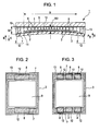
- Fig. 1 is a sectional side elevation showing a schematic structure of a display device according to an embodiment of the invention.
- Fig. 2 is a plan view showing an interior side of a first substrate.
- Fig. 3 is a plan view showing an interior side of a first substrate.
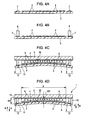
- Figs. 4A to 4D are schematic diagrams used for describing a method for fabricating a display device step by step.
- Fig. 5 is a schematic structural diagram used for describing a display device according to another embodiment of the invention.
- Fig. 6 is a perspective view showing an external structure of a computer, which is an example of the electronic apparatus of the invention.
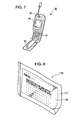
- Fig. 7 is a perspective view showing an external structure of a mobile phone, which is an example of the electronic apparatus of the invention.
- Fig. 8 is a perspective view showing an external structure of a sheet of electronic paper, which is an example of the electronic apparatus of the invention.
- Fig. 9 is a perspective view showing an external structure of an electronic notebook, which is an example of the electronic apparatus of the invention.
- Fig. 1 is a schematic diagram showing a display device according to an embodiment of the invention.
- reference numeral 1 represents a display device.
- the device is schematically shown with the size and shape being extremely changed from the actual size and shape.
- microcapsules in the center and microcapsules at both ends are shown to have different diameters, all the microcapsules are actually formed so as to have substantially the same diameter.
- the display device 1 includes a first substrate 3 provided with a plurality of pixel electrodes 2 and a second substrate 5 provided with a common electrode (counter electrode) 4. Microcapsules 6 encapsulating a display material are sandwiched between the first substrate 3 and the second substrate 5.
- a display device 1 can be designed so as to have one display surface (view surface) or two display surfaces (view surfaces).
- the substrate and electrode on the display surface side must have high light transmission properties, and in particular, are preferably transparent.
- the second substrate 5 is a transparent substrate and the common electrode 4 is a transparent electrode.
- the second substrate 5 side is a display surface.
- pixel electrodes 2 are disposed on the inner surface of the first substrate 3, and also wiring formed by a copper foil pattern or the like (not shown), which is connected to the pixel electrodes 2, is disposed thereon. Furthermore, substrate electrodes 7 are disposed outside the pixel electrodes 3 at the perimeter of the first substrate 3. The substrate electrodes 7 are each electrically connected to an external power source, for example, through a flexible printed circuit board (FPC), and electrically connected to the second substrate 5 through a conductive material 8.
- FPC flexible printed circuit board
- each of the first substrate 3 and the second substrate 5 a rectangular, film-shaped or sheet-shaped resin substrate is used in particular when the display device 1 is used for an IC card, electronic paper, or the like that is required to have flexibility.
- the second substrate 5 which serves as a display surface (view surface) as described above, a transparent substrate (having high light transmission properties) is used as described above.
- the material for such a transparent substrate (second substrate 5) for example, polyethylene terephthalate (PET), polyethersulfone (PES), or polycarbonate (PC) is preferably used.
- polyesters such as polyimide (PI) and polyethylene naphthalate (PEN), polyethylene (PE), polystyrene (PS), polypropylene (PP), polyetheretherketone (PEEK), acrylates or polyacrylates, and the like can also be used.
- PI polyimide
- PEN polyethylene naphthalate
- PS polystyrene
- PP polypropylene
- PEEK polyetheretherketone
- acrylates or polyacrylates and the like
- the display device is not required to have flexibility as in the case of the general panel, glass, hard resins, and semiconductor substrates composed of silicon or the like can also be used.
- a structure is employed in which at least one of the first substrate 3 and the second substrate 5 is elastically deformed and resilience is exerted in that state, and thus at least one of the first substrate 3 and the second substrate 5 must be an elastically deformable, flexible substrate.
- the material, thickness, etc. are appropriately selected for use in order to provide such properties.
- the first substrate 3 a polyimide substrate with a thickness of 25 ⁇ m is used, and thus the first substrate 3 has flexibility and is elastically deformable and resilient.
- a pair of substrate electrodes 7 are disposed on the inner surface of the polyimide substrate (first substrate 3) at the perimeter of the substrate, and pixel electrodes (not shown) are disposed between the substrate electrodes 7.
- a display area 9, which will be described below, is formed corresponding to the group of pixel electrodes.
- the substrate electrodes 7 are each composed of a copper foil pattern with a thickness of 10 to 20 ⁇ m, for example, formed by a semiadditive method.
- the pixel electrodes 2 may be formed by a copper foil pattern in the same step as that of forming the substrate electrodes 7, or may be formed using a general conductive material, such as aluminum (A1) separately from the formation of the substrate electrodes 7.
- Many pixel electrodes 2 are disposed in accordance with the predetermined pixel shape, such as a rectangular shape, that is designed in advance.
- the transparent electrode as the common electrode 4 is disposed on the inner surface of the transparent substrate (second substrate 5).
- the transparent electrode (common electrode 4) is formed over the entire inner surface of the second substrate 5, and is composed of a conductive oxide, such as indium-tin oxide (ITO), an electronically conductive polymer, such as polyaniline, an ionically conductive polymer prepared by dispersing an ionic substance, such as NaCl, LiClO 4 , or KCl, in a matrix resin, such as a polyvinyl alcohol resin or a polycarbonate resin, or the like.
- the transparent electrode (common electrode 4) is composed of an ITO film formed by vapor deposition or the like.
- Microcapsules 6 are disposed, in particular, on the pixel electrodes 2 between the first substrate 3 and the second substrate 5 having the structures described above. Thus, the microcapsules 6 constitute the display area 9 shown in Fig. 2. As described above, the microcapsules 6 encapsulate a display material, and all the microcapsules 6 are formed with substantially the same diameter. In this embodiment, the diameter is about 30 ⁇ m. The optical properties of the display material encapsulated change in response to electrical stimulation. Specifically, the display material is mainly composed of electrophoretic particles or a liquid crystal.
- an electrophoretic dispersion liquid including electrophoretic particles and a liquid-phase dispersion medium for dispersing the electrophoretic particles is used.
- the liquid-phase dispersion medium include water; alcohol solvents, such as methanol, ethanol, isopropanol, butanol, octanol, and methyl cellosolve; esters, such as ethyl acetate and butyl acetate; ketones, such as acetone, methyl ethyl ketone, and methyl isobutyl ketone; aliphatic hydrocarbons, such as pentane, hexane, and octane; alicyclic hydrocarbons, such as cyclohexane and methylcyclohexane; aromatic hydrocarbons, such as benzene, toluene, xylene, and long-chain alkyl group-containing benzenes, e.g.,
- the electrophoretic particles are organic or inorganic particles (polymer or colloid) which move by electrophoresis caused by the potential difference in the liquid-phase dispersion medium.
- the electrophoretic particles include black pigments, such as aniline black, carbon black, and titanium black; white pigments, such as titanium dioxide, zinc oxide, and antimony trioxide; yellow pigments, such as isoindolinone, chrome yellow, yellow iron oxide, cadmium yellow, titanium yellow, and antimony; azo pigments, such as monoazo, disazo, and polyazo; red pigments, such as quinacridone red and chrome vermillion; blue pigments, such as phthalocyanine blue, indanthrene blue, anthraquinone dyes, Prussian blue, ultramarine blue, and cobalt blue; and green pigments, such as phthalocyanine green. These pigments may be used alone or in combination of two or more.
- these pigments can be incorporated with an electrolyte, a surfactant, a charge controlling agent composed of particles of a metal soap, a resin, rubber, oil, varnish, a compound, or the like, a dispersing agent, such as a titanium coupling agent, an aluminum coupling agent, or a silane coupling agent, a lubricant, a stabilizer, or the like.
- a material for forming the wall membrane of the microcapsules 6 a gum arabic-gelatin composite membrane, or a compound, such as a urethane resin or a urea resin, can be used.
- two types of electrophoretic particles are encapsulated in the microcapsules 6.
- the particles of one type are negatively charged, and the particles of the other type are positively charged.
- the two types of electrophoretic particles for example, titanium dioxide, which is a white pigment, and carbon black, which is a black pigment, are used.
- white and black electrophoretic particles for example, when numbers and the like are displayed, the numbers and the like can be displayed by the black electrophoretic particles.
- display may be performed by using only one type of electrophoretic particles and subjecting the particles to electrophoresis toward the common electrode 4 or the pixel electrodes 2.
- the microcapsules 6 are fixed, in particular, on the common electrode 4 of the second substrate 5 with a binder 10.
- a binder 10 any material that has good affinity for the wall membrane of the microcapsule 6, excellent adhesion to the common electrode 4, and insulating properties can be used.
- Examples thereof include polyethylene, chlorinated polyethylene, ethylene-vinyl acetate copolymers, ethylene-ethyl acrylate copolymers, polypropylene, ABS resins, methyl methacrylate resins, vinyl chloride resins, vinyl chloride-vinyl acetate copolymers, vinyl chloride-vinylidene chloride copolymers, vinyl chloride-acrylate copolymers, vinyl chloride-methacrylic acid copolymers, vinyl chloride-acrylonitrile copolymers, ethylene-vinyl alcohol-vinyl chloride copolymers, propylene-vinyl chloride copolymers, vinylidene chloride resins, vinyl acetate resins, polyvinyl alcohol, polyvinyl formal, thermoplastic resins, such as cellulosic resins, polyamide resins, polymers, such as polyacetal, polycarbonate, polyethylene terephthalate, polybutylene terephthalate, polyphenylene oxide, polysul
- the microcapsules 6 are fixed on the pixel electrodes 2 of the first substrate 3 by a double-faced adhesive sheet 11.
- the double-faced adhesive sheet 11 has a thickness of about 25 ⁇ m and is composed of rubber, an acrylic resin, or the like having adhesion.
- the double-faced adhesive sheet 11 is bonded to the pixel electrodes 2 of the first substrate 3 and bonded to the microcapsules 6, thus holding the microcapsules 6 on the first substrate 3.
- the microcapsules 6 are sandwiched between the first substrate 3 and the second substrate 5 to constitute the display area 9.
- the substrate electrodes 7 are disposed outside the display area 9 as shown in Fig. 2, and a conductive material 8 is disposed on the substrate electrodes 7.
- the conductive material 8 together with each substrate electrode 7 constitutes a vertically conducting portion 12 which conducts between the first substrate 3 and the second substrate 5.
- the conductive material 8 is composed of a resin and conductive particles incorporated therein. That is, the conductive material 8 is composed of a conductive paste prepared by mixing conductive particles into a resin, such as an epoxy resin, the conductive particles formed by subjecting cores composed of metal particles, such as silver or nickel particles formed by crushing, carbon particles, or a resin, to nickel-plating and gold-plating, or a conductive sheet produced by forming the conductive paste into a sheet.
- the resin as a resin having adhesion at normal temperature, the rubber or the acrylic resin used for the double-faced adhesive sheet 11 is also preferably used.
- the thickness of the conductive material 8 which, together with the substrate electrode 7, constitutes the vertically conducting portion 12 is set such that the distance W1 between the first substrate 3 and the second substrate 5 at the vertically conducting portion 12 is larger than the distance W2 between the first substrate 3 and the second substrate 5 in the display area.
- the distance W1 between the first substrate 3 and the second substrate 5 at the vertically conducting portion 12 is substantially equal to the total thickness of the substrate electrode 7, the conductive material 8, and the common electrode 4, and the distance W2 between the first substrate 3 and the second substrate 5 in the display area is substantially equal to the total of the thickness of the pixel electrode 2 and the double-faced adhesive sheet 11, the thickness of the microcapsules 6 and the binder 10, and the thickness of the common electrode 4. Consequently, by setting the thickness of the conductive material 8 larger than the total of the diameter of the microcapsule 6 and the thickness of the double-faced adhesive sheet 11, the distance W1 can be set larger than the distance W2.
- the vertically conducting portion 12 sides, i.e., outer ends, of the first substrate 3, which has a particularly small thickness, are elastically deformed (warped) outward in a direction indicated by arrow A in Fig. 1.
- the first substrate 3 due to the resilience thereof, exerts force that acts inward as indicated by arrow B in Fig. 1, i.e., force that presses the conductive material 8 side.
- the largeness of the distance W1 with respect to the distance W2, i.e., the difference between the distance W1 and the distance W2, is preferably in the range of 10 to 200 ⁇ m, and particularly preferably in the range of 50 to 80 ⁇ m. If the difference is less than 10 ⁇ m, the pressing force due to the resilience toward the conductive material 8 is decreased, and there is a possibility that separation may occur in the reliability test. If the difference exceeds 200 ⁇ m, there is a possibility that, because of the change with time for a long period of time, the microcapsules 6 lying in the vicinity of the vertically conducting portion may be separated from the substrate 3(5), resulting in defective display.
- the thickness of the conductive material 8 such that the difference between the distance W1 and the distance W2 is in the range of 10 to 200 ⁇ m, both long-term reliability on defective continuity and long-term reliability on defective display can be ensured. In particular, by specifying the range of 50 to 80 ⁇ m, the long-term reliability can be more satisfactorily ensured.
- the conductive material 8 constituting the vertically conducting portion 12 is not disposed over the entire surface of each substrate electrode 7 and is disposed on a part of the upper surface of the substrate electrode 7. Consequently, a region in which the substrate electrode 7 and the conductive material 8 are stacked corresponds to the vertically conducting portion 12 in the invention.
- the adhesive layer 13 is disposed on the substrate electrode 7 at a position not provided with the conductive material 18 and in the vicinity thereof. As described above, the adhesive layer 13 is disposed at a position different from that of the vertically conducting portion 12 and also from that of the display area 9.
- the adhesive layer 13 is composed of a resin that has stronger adhesion than that of the conductive material 8 since the adhesive layer 13 is provided on the substrate electrode 7, adhesion between the substrate electrode 7 and the conductive material 8 is reinforced, and separation therebetween is prevented. Furthermore, when the adhesive layer 13 is composed of a moisture-resistant resin, in particular, by disposing the adhesive layer 13 in the vicinity of the substrate electrode 7 outside the vertically conducting portion 12 and the display area 9 so as to surround the vertically conducting portion 12 and the display area 9, it is possible to prevent corrosion of the electrode due to damp (moisture), degradation of the microcapsules, and the like.
- the moisture-resistant resin a resin having high crosslinking density, such as an epoxy resin, is used.
- the conductive material 8 is disposed on the substrate electrode 7 at one position, and one vertically conducting portion 12 is formed on one substrate electrode 7.
- the conductive material 8 may be disposed on the substrate electrode 7 at a plurality of (e.g., three) positions, and a plurality of vertically conducting portions 12 may be formed on one substrate electrode 7.
- the adhesive layer 13 between the plurality of portions of the conductive material 8, as described above, bonding between the substrate electrode 7 and the conductive material 8 can be reinforced, and separation therebetween can be prevented.
- a first substrate 3 composed of an elastically deformable polyimide with a thickness of about 25 ⁇ m is prepared, and substrate electrodes 7 and pixel electrodes 2 are formed thereon by a known method, such as the semiadditive method.
- the conductive sheet described above, as a conductive material 8 is disposed at a predetermined position of each substrate electrode 7 and bonded thereto.
- the thickness of the conductive sheet, serving as the conductive material 8 is set as a predetermined thickness such that the distance W1 is larger than the distance W2 in Fig. 1 as described above.
- a transparent substrate composed of polyethylene terephthalate (PET) is prepared, and a transparent electrode (common electrode 4) composed of ITO is formed over one surface (inner surface) thereof by vapor deposition or the like.
- a transparent electrode composed of ITO is formed over one surface (inner surface) thereof by vapor deposition or the like.
- many microcapsules 6 are bonded to a predetermined position on the common electrode 4 of the second substrate 5, i.e., the position corresponding to the display area 9, using a binder 10.
- a double-faced adhesive sheet 11 is bonded to a side opposite to the second substrate 5 side of the microcapsules 6.
- the second substrate 5 to which the double-faced adhesive sheet 11 has been thus bonded is disposed on the first substrate 3 so as to face the first substrate 3.
- the double-faced adhesive sheet 11 of the second substrate 5 is pressed against the surface of the first substrate 3 provided with the pixel electrodes 2 and the double-faced adhesive sheet 11 is bonded thereto.
- the common electrode 4 of the second substrate 5 is pressed against the conductive material 8 on the first substrate 3, and bonding therebetween is performed.
- the first substrate 3 and the second substrate 5 are integrated with the conductive material 8, the double-faced adhesive sheet 11, and the like therebetween, and the microcapsules 6 are sandwiched between the first substrate 3 and the second substrate 5.
- bonding of the double-faced adhesive sheet 11 and fixing by the conductive material 8 are basically performed at normal temperature without heating, and as necessary, heating is performed within a range that does not adversely affect the microcapsules 6.
- the distance W1 between the first substrate 3 and the second substrate 5 at the vertically conducting portion 12 becomes larger than the distance W2 between the first substrate 3 and the second substrate 5 in the display area 9.
- the perimeter of the first substrate 3 is elastically deformed (warped) outward, and resilience acts in a direction opposite to the direction of elastic deformation.
- an adhesive is injected into the space between the first substrate 3 and the second substrate 5 from the perimeter side with a dispenser or the like to dispose the adhesive at a portion in which the conductive material 8 is not disposed on the substrate electrode 7 and its vicinity, i.e., as shown in Fig. 4D, at a position surrounding the conductive portion 12 and the display area 9. Then, by curing the adhesive, an adhesive layer 13 is formed, and a display device 1 is thereby obtained.
- the adhesive a UV-curing type adhesive or the like that is cured without heating is used. However, as in the bonding treatment of the double-faced adhesive sheet 11 or the like, it is also possible to use an adhesive that is cured by heating within a range that does not adversely affect the microcapsules 6.
- the vertically conducting portion 12 is formed by setting the thickness of the conductive material 8 such that the distance W1 between the substrates at the vertically conducting portion 12 is larger than the distance between the substrates in the display area 9.
- the first substrate 3 due to the resilience thereof, exerts force that presses the conductive material 18 side as indicated by arrow B in Fig. 1 in particular, at the vertically conducting portion 12. Since the first substrate 3 presses the conductive material 8 side in such a manner, for example, even if a reliability test, such as a high-temperature preservation test or a temperature cycling test, is performed, separation between the first substrate 3 or the second substrate 5 and the conductive material 8 is prevented, and thus long-term reliability as a product is ensured.
- a reliability test such as a high-temperature preservation test or a temperature cycling test
- the invention is not limited to the embodiment described above. It is to be understood that various alterations may be made to the embodiment without departing from the spirit and scope of the invention.
- a double-faced adhesive sheet having a thickness of 25 ⁇ m or more may be used as the double-faced adhesive sheet 11.
- the double-faced adhesive sheet 11 When such a double-faced adhesive sheet 11 is used and the double-faced adhesive sheet 11 is pressed against the surface of the first substrate 3 provided with the pixel electrodes 2 for bonding and fixing, for example, by heating at a temperature of 50°C or higher (the temperature within a range that does not adversely affect the microcapsules 6), the double-faced adhesive sheet 11 is softened and a part thereof is allowed to protrude out toward the vertically conducting portion 12. Subsequently, curing is performed in that state. Thus, the portion allowed to protrude out between the microcapsules 6 and the vertically conducting portion 12 is used as an adhesive layer 14 as shown in Fig. 5.
- an adhesive is injected into the space between the first substrate 3 and the second substrate 5 from the perimeter side with a dispenser or the like, and the adhesive is cured to form an adhesive layer 13. Thereby, a display device is obtained.
- the same advantageous effect as that in the display device 1 is obtained.
- bonding between the first substrate 3 and the second substrate 5 is stronger, and bonding in the vicinity of the vertically conducting portion 12 is stronger.
- separation of the vertically conducting portion 12 from the first substrate 3 or the second substrate 5 can be reliably prevented.
- the adhesive layer 14 is formed using the double-faced adhesive sheet 11 simultaneously with the step of sandwiching the microcapsules between the first substrate 3 and the second substrate 5, the adhesive layer 14 can be formed without an additional step, thus facilitating the fabrication process.
- the first substrate 3 provided with the pixel electrodes 2 is elastically deformed outward by setting the thickness of the first substrate 3 smaller than that of the second substrate 5 provided with the common electrode 4 or the like.
- the second substrate 5 may be designed to be resilient.
- both substrates may be elastically deformed to allow each substrate to exert resilience.
- a case in which one display area is present has been described.
- the invention is also applicable to a case in which a plurality of display areas are each independently formed like an island.
- the electronic apparatuses according to some embodiments of the invention each include the display device according to the embodiment of the invention described above. Examples of the electronic apparatus including the display device will be described below.
- Fig. 6 is a perspective view showing a structure of the personal computer.
- a personal computer 80 includes a main body 82 provided with a keyboard 81 and a display unit provided with the display device 64.
- Fig. 7 is a perspective view showing a structure of the mobile phone.
- a mobile phone 90 includes a plurality of operation buttons 91, an earpiece 92, a mouthpiece 93, and the display device 64.
- FIG. 8 is a perspective view showing a structure of the electronic paper.
- Electronic paper 110 includes a main body 111 composed of a rewritable sheet having texture like paper and flexibility and a display unit provided with the display device 64.
- Fig. 9 is a perspective view showing a structure of an electronic notebook.
- an electronic notebook 120 includes a plurality of sheets of electronic paper 110 shown in Fig. 8, which are bundled together and covered with a cover 121.
- the display content of the electronic paper can be changed in the bundled state.
- the electronic apparatuses since the display device in which long-term reliability is ensured is provided, the electronic apparatuses each itself have also ensured long-term reliability.
- Examples of the electronic apparatus include, in addition to the personal computer shown in Fig. 6, the mobile phone shown in Fig. 7, the electronic paper shown in Fig. 8, and the electronic notebook shown in Fig. 9, IC cards each including a display provided with the display device, a fingerprint detection sensor, and the like, electronic books, viewfinder type or monitor-direct-view type video tape recorders, car navigation systems, pagers, electronic pocket diaries, desktop electronic calculators, word processors, workstations, television telephones, POS terminals, and apparatuses provided with touch panels.
- the display device can be used as a display for each of the various types of electronic apparatuses.
Landscapes
- Physics & Mathematics (AREA)
- Nonlinear Science (AREA)
- General Physics & Mathematics (AREA)
- Optics & Photonics (AREA)
- Chemical & Material Sciences (AREA)
- Crystallography & Structural Chemistry (AREA)
- Mathematical Physics (AREA)
- Health & Medical Sciences (AREA)
- Life Sciences & Earth Sciences (AREA)
- Chemical Kinetics & Catalysis (AREA)
- Electrochemistry (AREA)
- Molecular Biology (AREA)
- Electrochromic Elements, Electrophoresis, Or Variable Reflection Or Absorption Elements (AREA)
Abstract
Description
- The present invention relates to a display device provided with microcapsules and an electronic apparatus including the display device.
- Hitherto, electrophoretic display devices, each of which includes an electrophoretic dispersion liquid containing a liquid-phase dispersion medium and electrophoretic particles and utilizes the phenomenon in that the distribution state of the electrophoretic particles changes in the presence of an applied electric field, thus changing the optical properties of the electrophoretic dispersion liquid, have been known (for example, refer to
Japanese Unexamined Patent Application Publication No. 9-185087 - Furthermore, in a known electrophoretic display device, an electrophoretic dispersion liquid is encapsulated in microcapsules, and the microcapsules are sandwiched, for example, between a transparent substrate provided with a transparent electrode which serves as a common electrode and a substrate provided with pixel electrodes. Encapsulation of the electrophoretic dispersion liquid in microcapsules is advantageous in that it is possible to prevent the dispersion liquid from flowing out during the fabrication process of the display device, and it is possible to decrease sedimentation and aggregation of the electrophoretic particles.
- In such an electrophoretic display device provided with microcapsules, as a method for providing conduction between the transparent electrode and the substrate, a technique of using a conductive material including a resin and conductive particles incorporated therein is generally employed. As the conductive material, a conductive paste including a resin, such as epoxy, and conductive particles, such as metal particles, e.g., silver, or carbon particles, are incorporated therein, or a conductive sheet produced by forming the conductive paste into a sheet is known.
- When conduction is achieved between the substrates using such a conductive material, in order to prevent the occurrence of color irregularity and the like, the thickness (height) of the conductive material is set so that the distance between the substrates in the display area composed of the microcapsules is the same as the distance between the substrates at a vertically conducting portion which is conducted by the conductive material, and the vertically conducting portion is formed.
- However, in the display device having the structure described above, when reliability tests, such as a high-temperature preservation test and a temperature cycling test, are performed, in some cases, separation may occur between the transparent substrate or the substrate and the conductive material due to thermal expansion and thermal shrinkage of the resin in the conductive material, resulting in defective continuity. When defective continuity occurs in such reliability tests, it is expected that long-term reliability may not be ensured when the product is in the market. Therefore, it has been strongly demanded to take measures against the problems.
- An advantage of the invention is that it provides a display device in which occurrence of defective continuity resulting from separation between a substrate and a conductive material is prevented and long-term reliability is ensured, and an electronic apparatus including the display device.
- According to an aspect of the invention, a display device includes a first substrate, a second substrate, and microcapsules sandwiched between the first substrate and the second substrate, the microcapsules constituting a display area, the microcapsules encapsulating a display material whose optical properties change in response to electrical stimulation, wherein a conductive material for conducting between the substrates is provided between the first substrate and the second substrate to constitute a vertically conducting portion, and wherein the thickness of the conductive material is set such that the distance between the first substrate and the second substrate at the vertically conducting portion is larger than the distance between the first substrate and the second substrate in the display area.
- In the display device, the thickness of the conductive material is set such that the distance between the first substrate and the second substrate at the vertically conducting portion is larger than the distance between the first substrate and the second substrate in the display area. Thus, the first substrate and/or the second substrate are/is warped outward at the vertically conducting portion and elastically deformed with respect to the display area. Consequently, the first substrate and/or the second substrate, due to the resilience thereof, exert/exerts force that acts inward, i.e., force that presses the conductive material side, in particular at the vertically conducting portion. Since the first substrate and/or the second substrate always press/presses the conductive material side in such a manner, for example, even if a reliability test, such as a high-temperature preservation test or a temperature cycling test, is performed, separation between the first substrate or the second substrate and the conductive material is prevented, and thus long-term reliability as a product is ensured.
- In the display device, preferably, the thickness of the conductive material is set such that the distance between the first substrate and the second substrate at the vertically conducting portion is larger than the distance between the first substrate and the second substrate in the display area by a range of 10 to 200 µm. If the difference of the distance between the substrates at the vertically conducting portion is less than 10 µm, the pressing force due to the resilience toward the conductive material is decreased, and there is a possibility that separation may occur in the reliability test. If the difference exceeds 200 µm, there is a possibility that, because of the change with time for a long period of time, the microcapsules lying in the vicinity of the vertically conducting portion may be separated from the substrates, resulting in defective display. Consequently, by specifying the range of 10 to 200 µm, both long-term reliability on defective continuity and long-term reliability on defective display can be ensured.
- Furthermore, in the display device, preferably, the vertically conducting portion is disposed at the perimeter of each of the first substrate and the second substrate. In such a manner, since the resilience acts more strongly, the force that presses the conductive material side is more satisfactorily exerted.
- Furthermore, in the display device, preferably, an adhesive layer which bonds the first substrate to the second substrate is provided between the first substrate and the second substrate at a position different from that of the vertically conducting portion and from that of the display area. In such a manner, the first substrate and the second substrate are bonded to each other more strongly, and thus separation between each substrate and the conductive material can be prevented.
- Furthermore, in the display device, preferably, a substrate electrode is disposed on one of the first substrate and the second substrate at a position including the vertically conducting portion, and the adhesive layer is provided on the substrate electrode excluding a position at which the vertically conducting portion is disposed. In such a manner, in particular bonding between the substrate electrode and the conductive material can be reinforced by the adhesive layer.
- Furthermore, in the display device, preferably, the adhesive layer is provided between the microcapsules and the vertically conducting portion. In such a manner, the first substrate and the second substrate are bonded to each other more strongly, and also bonding in the vicinity of the vertically conducting portion becomes stronger, thus preventing separation of the vertically conducting portion from the first substrate or the second substrate.
- Furthermore, in the display device, preferably, the microcapsules are bonded to the first substrate or the second substrate, and an adhesive of the adhesive layer is the same as an adhesive for bonding the microcapsules to the first substrate or the second substrate. In such a manner, the step of forming the adhesive layer can be carried out simultaneously with the step of sandwiching the microcapsules, thus being advantageous in terms of the production process.
- Furthermore, preferably, the microcapsules are bonded to the first substrate or the second substrate with an adhesive sheet having a thickness of 25 µm or more, and the adhesive of the adhesive layer is formed by a portion of the adhesive sheet protruded out toward the vertically conducting portion. By using the adhesive sheet with a thickness of 25 µm or more and heating the adhesive sheet, the adhesive sheet is softened, and a portion thereof protrudes out toward the vertically conducting portion. The adhesive sheet is hardened in such a state to constitute the adhesive layer. Consequently, the adhesive layer can be formed without adding a new processing step, thus being extremely advantageous in terms of the production process.
- Furthermore, in the display device, preferably, the adhesive layer is composed of a moisture-resistant resin, and the adhesive layer is disposed outside the vertically conducting portion and the display area so as to surround the vertically conducting portion and the display area. In such a manner, it is possible to prevent corrosion of the electrode due to damp (moisture), degradation of the microcapsules, and the like.
- According to another aspect of the invention, an electronic apparatus includes the display device described above. Since the electronic apparatus includes the display device in which long-term reliability is ensured, the electronic apparatus itself has also ensured long-term reliability.
- The invention will be described with reference to the accompanying drawings, wherein like numbers reference like elements.
- Fig. 1 is a sectional side elevation showing a schematic structure of a display device according to an embodiment of the invention.
- Fig. 2 is a plan view showing an interior side of a first substrate.
- Fig. 3 is a plan view showing an interior side of a first substrate.
- Figs. 4A to 4D are schematic diagrams used for describing a method for fabricating a display device step by step.
- Fig. 5 is a schematic structural diagram used for describing a display device according to another embodiment of the invention.
- Fig. 6 is a perspective view showing an external structure of a computer, which is an example of the electronic apparatus of the invention.
- Fig. 7 is a perspective view showing an external structure of a mobile phone, which is an example of the electronic apparatus of the invention.
- Fig. 8 is a perspective view showing an external structure of a sheet of electronic paper, which is an example of the electronic apparatus of the invention.
- Fig. 9 is a perspective view showing an external structure of an electronic notebook, which is an example of the electronic apparatus of the invention.
- The invention will be described in detail below. Fig. 1 is a schematic diagram showing a display device according to an embodiment of the invention. In Fig. 1,
reference numeral 1 represents a display device. Note that, in Figs. 1 and 4A to 4D, in order to facilitate understanding of the characteristic parts of the invention, the device is schematically shown with the size and shape being extremely changed from the actual size and shape. In particular, although microcapsules in the center and microcapsules at both ends are shown to have different diameters, all the microcapsules are actually formed so as to have substantially the same diameter. - The
display device 1 includes afirst substrate 3 provided with a plurality ofpixel electrodes 2 and asecond substrate 5 provided with a common electrode (counter electrode) 4.Microcapsules 6 encapsulating a display material are sandwiched between thefirst substrate 3 and thesecond substrate 5. Such adisplay device 1 can be designed so as to have one display surface (view surface) or two display surfaces (view surfaces). The substrate and electrode on the display surface side must have high light transmission properties, and in particular, are preferably transparent. In this embodiment, as will be described below, thesecond substrate 5 is a transparent substrate and thecommon electrode 4 is a transparent electrode. Thus, thesecond substrate 5 side is a display surface. -
Many pixel electrodes 2 are disposed on the inner surface of thefirst substrate 3, and also wiring formed by a copper foil pattern or the like (not shown), which is connected to thepixel electrodes 2, is disposed thereon. Furthermore,substrate electrodes 7 are disposed outside thepixel electrodes 3 at the perimeter of thefirst substrate 3. Thesubstrate electrodes 7 are each electrically connected to an external power source, for example, through a flexible printed circuit board (FPC), and electrically connected to thesecond substrate 5 through aconductive material 8. - As each of the
first substrate 3 and thesecond substrate 5, a rectangular, film-shaped or sheet-shaped resin substrate is used in particular when thedisplay device 1 is used for an IC card, electronic paper, or the like that is required to have flexibility. Furthermore, as thesecond substrate 5 which serves as a display surface (view surface) as described above, a transparent substrate (having high light transmission properties) is used as described above. As the material for such a transparent substrate (second substrate 5), for example, polyethylene terephthalate (PET), polyethersulfone (PES), or polycarbonate (PC) is preferably used. - With respect to the
first substrate 3, which does not serve as a display surface, since transparency (high light transmission properties) is not required, in addition to the materials described above, polyesters, such as polyimide (PI) and polyethylene naphthalate (PEN), polyethylene (PE), polystyrene (PS), polypropylene (PP), polyetheretherketone (PEEK), acrylates or polyacrylates, and the like can also be used. Furthermore, when the display device is not required to have flexibility as in the case of the general panel, glass, hard resins, and semiconductor substrates composed of silicon or the like can also be used. - However, in the invention, as will be described below, a structure is employed in which at least one of the
first substrate 3 and thesecond substrate 5 is elastically deformed and resilience is exerted in that state, and thus at least one of thefirst substrate 3 and thesecond substrate 5 must be an elastically deformable, flexible substrate. The material, thickness, etc. are appropriately selected for use in order to provide such properties. - In this embodiment, as the
first substrate 3, a polyimide substrate with a thickness of 25 µm is used, and thus thefirst substrate 3 has flexibility and is elastically deformable and resilient. As shown in Fig. 2, a pair ofsubstrate electrodes 7 are disposed on the inner surface of the polyimide substrate (first substrate 3) at the perimeter of the substrate, and pixel electrodes (not shown) are disposed between thesubstrate electrodes 7. Adisplay area 9, which will be described below, is formed corresponding to the group of pixel electrodes. Thesubstrate electrodes 7 are each composed of a copper foil pattern with a thickness of 10 to 20 µm, for example, formed by a semiadditive method. - As shown in Fig. 1, the
pixel electrodes 2 may be formed by a copper foil pattern in the same step as that of forming thesubstrate electrodes 7, or may be formed using a general conductive material, such as aluminum (A1) separately from the formation of thesubstrate electrodes 7.Many pixel electrodes 2 are disposed in accordance with the predetermined pixel shape, such as a rectangular shape, that is designed in advance. - In this embodiment, as the
second substrate 5, a transparent substrate composed of polyethylene terephthalate (PET) with a thickness of 200 µm is used. As described above, the transparent electrode as thecommon electrode 4 is disposed on the inner surface of the transparent substrate (second substrate 5). The transparent electrode (common electrode 4) is formed over the entire inner surface of thesecond substrate 5, and is composed of a conductive oxide, such as indium-tin oxide (ITO), an electronically conductive polymer, such as polyaniline, an ionically conductive polymer prepared by dispersing an ionic substance, such as NaCl, LiClO4, or KCl, in a matrix resin, such as a polyvinyl alcohol resin or a polycarbonate resin, or the like. In this embodiment, the transparent electrode (common electrode 4) is composed of an ITO film formed by vapor deposition or the like. -
Microcapsules 6 are disposed, in particular, on thepixel electrodes 2 between thefirst substrate 3 and thesecond substrate 5 having the structures described above. Thus, themicrocapsules 6 constitute thedisplay area 9 shown in Fig. 2. As described above, themicrocapsules 6 encapsulate a display material, and all themicrocapsules 6 are formed with substantially the same diameter. In this embodiment, the diameter is about 30 µm. The optical properties of the display material encapsulated change in response to electrical stimulation. Specifically, the display material is mainly composed of electrophoretic particles or a liquid crystal. - As the material mainly composed of electrophoretic particles, an electrophoretic dispersion liquid including electrophoretic particles and a liquid-phase dispersion medium for dispersing the electrophoretic particles is used. Examples of the liquid-phase dispersion medium include water; alcohol solvents, such as methanol, ethanol, isopropanol, butanol, octanol, and methyl cellosolve; esters, such as ethyl acetate and butyl acetate; ketones, such as acetone, methyl ethyl ketone, and methyl isobutyl ketone; aliphatic hydrocarbons, such as pentane, hexane, and octane; alicyclic hydrocarbons, such as cyclohexane and methylcyclohexane; aromatic hydrocarbons, such as benzene, toluene, xylene, and long-chain alkyl group-containing benzenes, e.g., hexylbenzene, heptylbenzene, octylbenzene, nonylbenzene, decylbenzene, undecylbenzene, dodecylbenzene, tridecylbenzene, and tetradecylbenzene; halogenated hydrocarbons, such as methylene chloride, chloroform, carbon tetrachloride, and 1,2-dichloroethane; carboxylate salts; and various types of oil. These liquid-phase dispersion media may be used alone or in combination together with a surfactant or the like.
- The electrophoretic particles are organic or inorganic particles (polymer or colloid) which move by electrophoresis caused by the potential difference in the liquid-phase dispersion medium. Examples of the electrophoretic particles include black pigments, such as aniline black, carbon black, and titanium black; white pigments, such as titanium dioxide, zinc oxide, and antimony trioxide; yellow pigments, such as isoindolinone, chrome yellow, yellow iron oxide, cadmium yellow, titanium yellow, and antimony; azo pigments, such as monoazo, disazo, and polyazo; red pigments, such as quinacridone red and chrome vermillion; blue pigments, such as phthalocyanine blue, indanthrene blue, anthraquinone dyes, Prussian blue, ultramarine blue, and cobalt blue; and green pigments, such as phthalocyanine green. These pigments may be used alone or in combination of two or more.
- Furthermore, as necessary, these pigments can be incorporated with an electrolyte, a surfactant, a charge controlling agent composed of particles of a metal soap, a resin, rubber, oil, varnish, a compound, or the like, a dispersing agent, such as a titanium coupling agent, an aluminum coupling agent, or a silane coupling agent, a lubricant, a stabilizer, or the like. As a material for forming the wall membrane of the
microcapsules 6, a gum arabic-gelatin composite membrane, or a compound, such as a urethane resin or a urea resin, can be used. - In the
display device 1 of this example, two types of electrophoretic particles are encapsulated in themicrocapsules 6. The particles of one type are negatively charged, and the particles of the other type are positively charged. As the two types of electrophoretic particles, for example, titanium dioxide, which is a white pigment, and carbon black, which is a black pigment, are used. By using such white and black electrophoretic particles, for example, when numbers and the like are displayed, the numbers and the like can be displayed by the black electrophoretic particles. Alternatively, display may be performed by using only one type of electrophoretic particles and subjecting the particles to electrophoresis toward thecommon electrode 4 or thepixel electrodes 2. - Furthermore, the
microcapsules 6 are fixed, in particular, on thecommon electrode 4 of thesecond substrate 5 with abinder 10. As thebinder 10, any material that has good affinity for the wall membrane of themicrocapsule 6, excellent adhesion to thecommon electrode 4, and insulating properties can be used. Examples thereof include polyethylene, chlorinated polyethylene, ethylene-vinyl acetate copolymers, ethylene-ethyl acrylate copolymers, polypropylene, ABS resins, methyl methacrylate resins, vinyl chloride resins, vinyl chloride-vinyl acetate copolymers, vinyl chloride-vinylidene chloride copolymers, vinyl chloride-acrylate copolymers, vinyl chloride-methacrylic acid copolymers, vinyl chloride-acrylonitrile copolymers, ethylene-vinyl alcohol-vinyl chloride copolymers, propylene-vinyl chloride copolymers, vinylidene chloride resins, vinyl acetate resins, polyvinyl alcohol, polyvinyl formal, thermoplastic resins, such as cellulosic resins, polyamide resins, polymers, such as polyacetal, polycarbonate, polyethylene terephthalate, polybutylene terephthalate, polyphenylene oxide, polysulfone, polyamide-imide, polyaminobis-maleimide, polyethersulfone, polyphenylene sulfone, polyarylate, grafted polyphenylene ether, polyetheretherketone, and polyether imide, fluorocarbon resins, such as polytetrafluoroethylene, polyfluoroethylenepropylene, tetrafluoroethyleneperfluoroalkoxyethylene copolymers, ethylenetetrafluoroethylene copolymers, polyvinylidene fluoride, polytrifluoroethylene chloride, and fluororubber, and silicon resins, such as silicone resins and silicone rubber. Other examples include methacrylic acid-styrene copolymers, polybutylene, and methyl methacrylate-butadiene-styrene copolymers. - The
microcapsules 6 are fixed on thepixel electrodes 2 of thefirst substrate 3 by a double-facedadhesive sheet 11. The double-facedadhesive sheet 11 has a thickness of about 25 µm and is composed of rubber, an acrylic resin, or the like having adhesion. The double-facedadhesive sheet 11 is bonded to thepixel electrodes 2 of thefirst substrate 3 and bonded to themicrocapsules 6, thus holding themicrocapsules 6 on thefirst substrate 3. By such a structure, themicrocapsules 6 are sandwiched between thefirst substrate 3 and thesecond substrate 5 to constitute thedisplay area 9. - The
substrate electrodes 7 are disposed outside thedisplay area 9 as shown in Fig. 2, and aconductive material 8 is disposed on thesubstrate electrodes 7. Theconductive material 8 together with eachsubstrate electrode 7 constitutes a vertically conductingportion 12 which conducts between thefirst substrate 3 and thesecond substrate 5. Theconductive material 8 is composed of a resin and conductive particles incorporated therein. That is, theconductive material 8 is composed of a conductive paste prepared by mixing conductive particles into a resin, such as an epoxy resin, the conductive particles formed by subjecting cores composed of metal particles, such as silver or nickel particles formed by crushing, carbon particles, or a resin, to nickel-plating and gold-plating, or a conductive sheet produced by forming the conductive paste into a sheet. In particular, with respect to the resin, as a resin having adhesion at normal temperature, the rubber or the acrylic resin used for the double-facedadhesive sheet 11 is also preferably used. - Here, with respect to the thickness of the
conductive material 8 which, together with thesubstrate electrode 7, constitutes the vertically conductingportion 12, the thickness of theconductive material 8 is set such that the distance W1 between thefirst substrate 3 and thesecond substrate 5 at the vertically conductingportion 12 is larger than the distance W2 between thefirst substrate 3 and thesecond substrate 5 in the display area. That is, the distance W1 between thefirst substrate 3 and thesecond substrate 5 at the vertically conductingportion 12 is substantially equal to the total thickness of thesubstrate electrode 7, theconductive material 8, and thecommon electrode 4, and the distance W2 between thefirst substrate 3 and thesecond substrate 5 in the display area is substantially equal to the total of the thickness of thepixel electrode 2 and the double-facedadhesive sheet 11, the thickness of themicrocapsules 6 and thebinder 10, and the thickness of thecommon electrode 4. Consequently, by setting the thickness of theconductive material 8 larger than the total of the diameter of themicrocapsule 6 and the thickness of the double-facedadhesive sheet 11, the distance W1 can be set larger than the distance W2. - By setting the distance W1 between the substrates at the vertically conducting
portion 12 larger than the distance W2 between the substrates in thedisplay area 9 in such a manner, as shown in Fig. 1, the vertically conductingportion 12 sides, i.e., outer ends, of thefirst substrate 3, which has a particularly small thickness, are elastically deformed (warped) outward in a direction indicated by arrow A in Fig. 1. As a result, thefirst substrate 3, due to the resilience thereof, exerts force that acts inward as indicated by arrow B in Fig. 1, i.e., force that presses theconductive material 8 side. - Here, the largeness of the distance W1 with respect to the distance W2, i.e., the difference between the distance W1 and the distance W2, is preferably in the range of 10 to 200 µm, and particularly preferably in the range of 50 to 80 µm. If the difference is less than 10µm, the pressing force due to the resilience toward the
conductive material 8 is decreased, and there is a possibility that separation may occur in the reliability test. If the difference exceeds 200 µm, there is a possibility that, because of the change with time for a long period of time, themicrocapsules 6 lying in the vicinity of the vertically conducting portion may be separated from the substrate 3(5), resulting in defective display. Consequently, by designing the thickness of theconductive material 8 such that the difference between the distance W1 and the distance W2 is in the range of 10 to 200 µm, both long-term reliability on defective continuity and long-term reliability on defective display can be ensured. In particular, by specifying the range of 50 to 80 µm, the long-term reliability can be more satisfactorily ensured. - There may be a case where a plurality of vertically conducting
portions 12 are present, and consequently, variation occurs in the distance W1 between the substrates at these vertically conductingportions 12. In such a case, the average of a plurality of distances W1 is considered as the distance W1 between the substrates at the vertically conductingportion 12 in the invention. As shown in Fig. 1, variation also occurs in the distance W2 between the substrates in thedisplay area 9. With respect to the distance W2, the minimum value of a plurality of distances W2 is considered as the distance W2 between the substrates in thedisplay area 9. - As shown in Fig. 2, the
conductive material 8 constituting the vertically conductingportion 12 is not disposed over the entire surface of eachsubstrate electrode 7 and is disposed on a part of the upper surface of thesubstrate electrode 7. Consequently, a region in which thesubstrate electrode 7 and theconductive material 8 are stacked corresponds to the vertically conductingportion 12 in the invention. Theadhesive layer 13 is disposed on thesubstrate electrode 7 at a position not provided with the conductive material 18 and in the vicinity thereof. As described above, theadhesive layer 13 is disposed at a position different from that of the vertically conductingportion 12 and also from that of thedisplay area 9. By disposing theadhesive layer 13 between thefirst substrate 3 and (thecommon electrode 4 of) thesecond substrate 5, thefirst substrate 3 and thesecond substrate 5 are fixed to each other and the substrates are bonded to each other more strongly. - In particular, when the
adhesive layer 13 is composed of a resin that has stronger adhesion than that of theconductive material 8, since theadhesive layer 13 is provided on thesubstrate electrode 7, adhesion between thesubstrate electrode 7 and theconductive material 8 is reinforced, and separation therebetween is prevented. Furthermore, when theadhesive layer 13 is composed of a moisture-resistant resin, in particular, by disposing theadhesive layer 13 in the vicinity of thesubstrate electrode 7 outside the vertically conductingportion 12 and thedisplay area 9 so as to surround the vertically conductingportion 12 and thedisplay area 9, it is possible to prevent corrosion of the electrode due to damp (moisture), degradation of the microcapsules, and the like. As the moisture-resistant resin, a resin having high crosslinking density, such as an epoxy resin, is used. - In Fig. 2, the
conductive material 8 is disposed on thesubstrate electrode 7 at one position, and one vertically conductingportion 12 is formed on onesubstrate electrode 7. However, as shown in Fig. 3, theconductive material 8 may be disposed on thesubstrate electrode 7 at a plurality of (e.g., three) positions, and a plurality of vertically conductingportions 12 may be formed on onesubstrate electrode 7. In such a case, by disposing theadhesive layer 13 between the plurality of portions of theconductive material 8, as described above, bonding between thesubstrate electrode 7 and theconductive material 8 can be reinforced, and separation therebetween can be prevented. - In order to fabricate a
display device 1 having the structure described above, first, as shown in Fig. 4A, afirst substrate 3 composed of an elastically deformable polyimide with a thickness of about 25 µm is prepared, andsubstrate electrodes 7 andpixel electrodes 2 are formed thereon by a known method, such as the semiadditive method. Subsequently, as shown in Fig. 4B, the conductive sheet described above, as aconductive material 8, is disposed at a predetermined position of eachsubstrate electrode 7 and bonded thereto. The thickness of the conductive sheet, serving as theconductive material 8, is set as a predetermined thickness such that the distance W1 is larger than the distance W2 in Fig. 1 as described above. - Furthermore, separately, as a
second substrate 5, a transparent substrate composed of polyethylene terephthalate (PET) is prepared, and a transparent electrode (common electrode 4) composed of ITO is formed over one surface (inner surface) thereof by vapor deposition or the like. Then,many microcapsules 6 are bonded to a predetermined position on thecommon electrode 4 of thesecond substrate 5, i.e., the position corresponding to thedisplay area 9, using abinder 10. Subsequently, a double-facedadhesive sheet 11 is bonded to a side opposite to thesecond substrate 5 side of themicrocapsules 6. - Subsequently, the
second substrate 5 to which the double-facedadhesive sheet 11 has been thus bonded is disposed on thefirst substrate 3 so as to face thefirst substrate 3. Then, as shown in Fig. 4C, the double-facedadhesive sheet 11 of thesecond substrate 5 is pressed against the surface of thefirst substrate 3 provided with thepixel electrodes 2 and the double-facedadhesive sheet 11 is bonded thereto. Simultaneously, thecommon electrode 4 of thesecond substrate 5 is pressed against theconductive material 8 on thefirst substrate 3, and bonding therebetween is performed. Thus, thefirst substrate 3 and thesecond substrate 5 are integrated with theconductive material 8, the double-facedadhesive sheet 11, and the like therebetween, and themicrocapsules 6 are sandwiched between thefirst substrate 3 and thesecond substrate 5. Note that bonding of the double-facedadhesive sheet 11 and fixing by theconductive material 8 are basically performed at normal temperature without heating, and as necessary, heating is performed within a range that does not adversely affect themicrocapsules 6. - By integrating the
first substrate 3 and thesecond substrate 5 in such a manner, the distance W1 between thefirst substrate 3 and thesecond substrate 5 at the vertically conductingportion 12 becomes larger than the distance W2 between thefirst substrate 3 and thesecond substrate 5 in thedisplay area 9. As a result, as shown in Fig. 4C, the perimeter of thefirst substrate 3 is elastically deformed (warped) outward, and resilience acts in a direction opposite to the direction of elastic deformation. - Subsequently, an adhesive is injected into the space between the
first substrate 3 and thesecond substrate 5 from the perimeter side with a dispenser or the like to dispose the adhesive at a portion in which theconductive material 8 is not disposed on thesubstrate electrode 7 and its vicinity, i.e., as shown in Fig. 4D, at a position surrounding theconductive portion 12 and thedisplay area 9. Then, by curing the adhesive, anadhesive layer 13 is formed, and adisplay device 1 is thereby obtained. As the adhesive, a UV-curing type adhesive or the like that is cured without heating is used. However, as in the bonding treatment of the double-facedadhesive sheet 11 or the like, it is also possible to use an adhesive that is cured by heating within a range that does not adversely affect themicrocapsules 6. - In the
display device 1 thus obtained, the vertically conductingportion 12 is formed by setting the thickness of theconductive material 8 such that the distance W1 between the substrates at the vertically conductingportion 12 is larger than the distance between the substrates in thedisplay area 9. Thus, as described above, thefirst substrate 3, due to the resilience thereof, exerts force that presses the conductive material 18 side as indicated by arrow B in Fig. 1 in particular, at the vertically conductingportion 12. Since thefirst substrate 3 presses theconductive material 8 side in such a manner, for example, even if a reliability test, such as a high-temperature preservation test or a temperature cycling test, is performed, separation between thefirst substrate 3 or thesecond substrate 5 and theconductive material 8 is prevented, and thus long-term reliability as a product is ensured. - The invention is not limited to the embodiment described above. It is to be understood that various alterations may be made to the embodiment without departing from the spirit and scope of the invention. For example, in the fabrication process of the
display device 1, when the double-facedadhesive sheet 11 is bonded to a side of themicrocapsules 6 bonded to thesecond substrate 5 opposite to thesecond substrate 5 side, as the double-facedadhesive sheet 11, a double-faced adhesive sheet having a thickness of 25µm or more may be used. When such a double-facedadhesive sheet 11 is used and the double-facedadhesive sheet 11 is pressed against the surface of thefirst substrate 3 provided with thepixel electrodes 2 for bonding and fixing, for example, by heating at a temperature of 50°C or higher (the temperature within a range that does not adversely affect the microcapsules 6), the double-facedadhesive sheet 11 is softened and a part thereof is allowed to protrude out toward the vertically conductingportion 12. Subsequently, curing is performed in that state. Thus, the portion allowed to protrude out between themicrocapsules 6 and the vertically conductingportion 12 is used as anadhesive layer 14 as shown in Fig. 5. - Subsequently, as in the case shown in Fig. 4D, an adhesive is injected into the space between the
first substrate 3 and thesecond substrate 5 from the perimeter side with a dispenser or the like, and the adhesive is cured to form anadhesive layer 13. Thereby, a display device is obtained. - In such a display device, the same advantageous effect as that in the
display device 1 is obtained. In addition, bonding between thefirst substrate 3 and thesecond substrate 5 is stronger, and bonding in the vicinity of the vertically conductingportion 12 is stronger. Thus, separation of the vertically conductingportion 12 from thefirst substrate 3 or thesecond substrate 5 can be reliably prevented. Furthermore, since theadhesive layer 14 is formed using the double-facedadhesive sheet 11 simultaneously with the step of sandwiching the microcapsules between thefirst substrate 3 and thesecond substrate 5, theadhesive layer 14 can be formed without an additional step, thus facilitating the fabrication process. - Furthermore, in the embodiment described above, the
first substrate 3 provided with thepixel electrodes 2 is elastically deformed outward by setting the thickness of thefirst substrate 3 smaller than that of thesecond substrate 5 provided with thecommon electrode 4 or the like. However, thesecond substrate 5 may be designed to be resilient. Alternatively, by designing thefirst substrate 3 and thesecond substrate 5 so as to have the same strength, both substrates may be elastically deformed to allow each substrate to exert resilience. Furthermore, in the embodiment, a case in which one display area is present has been described. The invention is also applicable to a case in which a plurality of display areas are each independently formed like an island. - Electronic apparatuses according to some embodiments of the invention will now be described below. The electronic apparatuses according to the embodiments of the invention each include the display device according to the embodiment of the invention described above. Examples of the electronic apparatus including the display device will be described below.
- First, an example in which the display device is applied to a mobile personal computer will be described.
Fig. 6 is a perspective view showing a structure of the personal computer. As shown in Fig. 6, apersonal computer 80 includes amain body 82 provided with akeyboard 81 and a display unit provided with thedisplay device 64. - Next, an example in which the display device is applied to a display of a mobile phone will be described. Fig. 7 is a perspective view showing a structure of the mobile phone. As shown in Fig. 7, a
mobile phone 90 includes a plurality ofoperation buttons 91, anearpiece 92, amouthpiece 93, and thedisplay device 64. - Next, an example in which the display device is applied to a display of electronic paper will be described. Fig. 8 is a perspective view showing a structure of the electronic paper.
Electronic paper 110 includes amain body 111 composed of a rewritable sheet having texture like paper and flexibility and a display unit provided with thedisplay device 64. - Fig. 9 is a perspective view showing a structure of an electronic notebook. As shown in Fig. 9, an
electronic notebook 120 includes a plurality of sheets ofelectronic paper 110 shown in Fig. 8, which are bundled together and covered with acover 121. By providing a display data input unit on thecover 121, the display content of the electronic paper can be changed in the bundled state. - According to the electronic apparatuses described above, since the display device in which long-term reliability is ensured is provided, the electronic apparatuses each itself have also ensured long-term reliability.
- Examples of the electronic apparatus include, in addition to the personal computer shown in Fig. 6, the mobile phone shown in Fig. 7, the electronic paper shown in Fig. 8, and the electronic notebook shown in Fig. 9, IC cards each including a display provided with the display device, a fingerprint detection sensor, and the like, electronic books, viewfinder type or monitor-direct-view type video tape recorders, car navigation systems, pagers, electronic pocket diaries, desktop electronic calculators, word processors, workstations, television telephones, POS terminals, and apparatuses provided with touch panels. Of course, the display device can be used as a display for each of the various types of electronic apparatuses.
Claims (10)
- A display device comprising:a first substrate;a second substrate; andmicrocapsules sandwiched between the first substrate and the second substrate, the microcapsules constituting a display area, the microcapsules encapsulating a display material whose optical properties change in response to electrical stimulation,wherein a conductive material for conducting between the substrates is provided between the first substrate and the second substrate to constitute a vertically conducting portion; and
wherein the thickness of the conductive material is set such that the distance between the first substrate and the second substrate at the vertically conducting portion is larger than the distance between the first substrate and the second substrate in the display area. - The display device according to Claim 1, wherein the thickness of the conductive material is set such that the distance between the first substrate and the second substrate at the vertically conducting portion is larger than the distance between the first substrate and the second substrate in the display area by a range of 10 to 200 µm.
- The display device according to Claim 1, wherein the vertically conducting portion is disposed at the perimeter of each of the first substrate and the second substrate.
- The display device according to Claim 1, wherein an adhesive layer which bonds the first substrate to the second substrate is provided between the first substrate and the second substrate at a position different from that of the vertically conducting portion and from that of the display area.
- The display device according to Claim 4, wherein a substrate electrode is disposed on one of the first substrate and the second substrate at a position including the vertically conducting portion, and the adhesive layer is provided on the substrate electrode excluding a position at which the vertically conducting portion is disposed.
- The display device according to Claim 4, wherein the adhesive layer is provided between the microcapsules and the vertically conducting portion.
- The display device according to Claim 6, wherein the microcapsules are bonded to the first substrate or the second substrate, and an adhesive of the adhesive layer is the same as an adhesive for bonding the microcapsules to the first substrate or the second substrate.
- The display device according to Claim 7, wherein the microcapsules are bonded to the first substrate or the second substrate with an adhesive sheet having a thickness of 25 µm or more, and the adhesive of the adhesive layer is formed by a portion of the adhesive sheet protruded out toward the vertically conducting portion.
- The display device according to Claim 4, wherein the adhesive layer is composed of a moisture-resistant resin, and the adhesive layer is disposed outside the vertically conducting portion and the display area so as to surround the vertically conducting portion and the display area.
- An electronic apparatus comprising the display device according to Claim 1.
Applications Claiming Priority (2)
| Application Number | Priority Date | Filing Date | Title |
|---|---|---|---|
| JP2005299838 | 2005-10-14 | ||
| JP2006159799A JP4508160B2 (en) | 2005-10-14 | 2006-06-08 | Display device and electronic device |
Publications (2)
| Publication Number | Publication Date |
|---|---|
| EP1775626A1 true EP1775626A1 (en) | 2007-04-18 |
| EP1775626B1 EP1775626B1 (en) | 2010-08-18 |
Family
ID=37450947
Family Applications (1)
| Application Number | Title | Priority Date | Filing Date |
|---|---|---|---|
| EP06021335A Not-in-force EP1775626B1 (en) | 2005-10-14 | 2006-10-11 | Display device and electronic apparatus |
Country Status (4)
| Country | Link |
|---|---|
| US (2) | US7528903B2 (en) |
| EP (1) | EP1775626B1 (en) |
| JP (1) | JP4508160B2 (en) |
| DE (1) | DE602006016207D1 (en) |
Cited By (1)
| Publication number | Priority date | Publication date | Assignee | Title |
|---|---|---|---|---|
| WO2008103039A1 (en) * | 2007-02-21 | 2008-08-28 | Polymer Vision Limited | A flexible display and a method of producing a flexible display |
Families Citing this family (6)
| Publication number | Priority date | Publication date | Assignee | Title |
|---|---|---|---|---|
| JP5167624B2 (en) * | 2005-12-28 | 2013-03-21 | セイコーエプソン株式会社 | Electrophoretic display device and electronic apparatus |
| JP2009170195A (en) * | 2008-01-15 | 2009-07-30 | Panasonic Corp | Movable contact body and switch using the same |
| JP2009170194A (en) * | 2008-01-15 | 2009-07-30 | Panasonic Corp | Touch panel and movable contact body and switch using the same |
| WO2013118508A1 (en) * | 2012-02-07 | 2013-08-15 | パナソニック株式会社 | Composite substrate, method for manufacturing same, and organic electroluminescence device |
| US8994677B2 (en) * | 2012-07-03 | 2015-03-31 | Innocom Technology (Shenzhen) Co., Ltd. | Touch sensing structure |
| CN107656408A (en) * | 2017-09-26 | 2018-02-02 | 无锡威峰科技股份有限公司 | Electronic-paper display screen and its manufacture method |
Citations (3)
| Publication number | Priority date | Publication date | Assignee | Title |
|---|---|---|---|---|
| US6525799B1 (en) * | 1998-11-27 | 2003-02-25 | Nanox Corporation | Liquid crystal display device having spacers with two sizes and metal films and protrusions |
| US20040027327A1 (en) * | 2002-06-10 | 2004-02-12 | E Ink Corporation | Components and methods for use in electro-optic displays |
| US20040135764A1 (en) * | 2002-10-21 | 2004-07-15 | Toshihiko Takeda | Process for producing display device |
Family Cites Families (5)
| Publication number | Priority date | Publication date | Assignee | Title |
|---|---|---|---|---|
| JP3991367B2 (en) | 1995-12-28 | 2007-10-17 | セイコーエプソン株式会社 | Electrophoresis device |
| JPH1048657A (en) | 1996-07-30 | 1998-02-20 | Ricoh Co Ltd | Polymer film liquid crystal display |
| JP3813829B2 (en) * | 2001-03-21 | 2006-08-23 | 株式会社東芝 | Electrophoretic display device |
| JP4573516B2 (en) * | 2002-10-29 | 2010-11-04 | パナソニック株式会社 | Display device |
| JP2005242320A (en) * | 2004-01-27 | 2005-09-08 | Canon Inc | Display device and display method thereof |
-
2006
- 2006-06-08 JP JP2006159799A patent/JP4508160B2/en not_active Expired - Fee Related
- 2006-09-13 US US11/531,415 patent/US7528903B2/en not_active Expired - Fee Related
- 2006-10-11 EP EP06021335A patent/EP1775626B1/en not_active Not-in-force
- 2006-10-11 DE DE602006016207T patent/DE602006016207D1/en active Active
-
2009
- 2009-03-24 US US12/409,885 patent/US7733442B2/en active Active - Reinstated
Patent Citations (3)
| Publication number | Priority date | Publication date | Assignee | Title |
|---|---|---|---|---|
| US6525799B1 (en) * | 1998-11-27 | 2003-02-25 | Nanox Corporation | Liquid crystal display device having spacers with two sizes and metal films and protrusions |
| US20040027327A1 (en) * | 2002-06-10 | 2004-02-12 | E Ink Corporation | Components and methods for use in electro-optic displays |
| US20040135764A1 (en) * | 2002-10-21 | 2004-07-15 | Toshihiko Takeda | Process for producing display device |
Cited By (2)
| Publication number | Priority date | Publication date | Assignee | Title |
|---|---|---|---|---|
| WO2008103039A1 (en) * | 2007-02-21 | 2008-08-28 | Polymer Vision Limited | A flexible display and a method of producing a flexible display |
| US7957051B2 (en) | 2007-02-21 | 2011-06-07 | Polymer Vision Limited | Flexible display and a method of producing a flexible display |
Also Published As
| Publication number | Publication date |
|---|---|
| US20070085945A1 (en) | 2007-04-19 |
| JP2007133359A (en) | 2007-05-31 |
| US20090185259A1 (en) | 2009-07-23 |
| EP1775626B1 (en) | 2010-08-18 |
| JP4508160B2 (en) | 2010-07-21 |
| US7528903B2 (en) | 2009-05-05 |
| DE602006016207D1 (en) | 2010-09-30 |
| US7733442B2 (en) | 2010-06-08 |
Similar Documents
| Publication | Publication Date | Title |
|---|---|---|
| US7660033B2 (en) | Electrophoretic display device and electronic apparatus | |
| US7835063B2 (en) | Electrophoretic device, electrophoretic display, and electronic apparatus | |
| US7733442B2 (en) | Display device and electronic apparatus | |
| US8717661B2 (en) | Electrophoresis device and electronic apparatus | |
| JP5510500B2 (en) | Electrophoretic display device and electronic apparatus | |
| JP5028799B2 (en) | Electro-optical device and electronic apparatus | |
| JP2010122706A (en) | Display and electronic apparatus | |
| JP2006259243A (en) | Electrophoretic display device, manufacturing method thereof, and electronic apparatus | |
| JP4899505B2 (en) | Electrophoretic display device and electronic apparatus | |
| JP4984463B2 (en) | Method for manufacturing electrophoresis apparatus | |
| JP4765398B2 (en) | Method for manufacturing electrophoretic display device | |
| JP2007171447A (en) | Electro-optical device, method of manufacturing electro-optical device, and electronic apparatus | |
| JP2007199245A (en) | Method for manufacturing electrophoretic display device and electronic apparatus |
Legal Events
| Date | Code | Title | Description |
|---|---|---|---|
| PUAI | Public reference made under article 153(3) epc to a published international application that has entered the european phase |
Free format text: ORIGINAL CODE: 0009012 |
|
| AK | Designated contracting states |
Kind code of ref document: A1 Designated state(s): AT BE BG CH CY CZ DE DK EE ES FI FR GB GR HU IE IS IT LI LT LU LV MC NL PL PT RO SE SI SK TR |
|
| AX | Request for extension of the european patent |
Extension state: AL BA HR MK YU |
|
| 17P | Request for examination filed |
Effective date: 20070412 |
|
| AKX | Designation fees paid |
Designated state(s): DE FR GB |
|
| GRAP | Despatch of communication of intention to grant a patent |
Free format text: ORIGINAL CODE: EPIDOSNIGR1 |
|
| GRAS | Grant fee paid |
Free format text: ORIGINAL CODE: EPIDOSNIGR3 |
|
| GRAA | (expected) grant |
Free format text: ORIGINAL CODE: 0009210 |
|
| AK | Designated contracting states |
Kind code of ref document: B1 Designated state(s): DE FR GB |
|
| REG | Reference to a national code |
Ref country code: GB Ref legal event code: FG4D |
|
| REF | Corresponds to: |
Ref document number: 602006016207 Country of ref document: DE Date of ref document: 20100930 Kind code of ref document: P |
|
| PLBE | No opposition filed within time limit |
Free format text: ORIGINAL CODE: 0009261 |
|
| STAA | Information on the status of an ep patent application or granted ep patent |
Free format text: STATUS: NO OPPOSITION FILED WITHIN TIME LIMIT |
|
| 26N | No opposition filed |
Effective date: 20110519 |
|
| REG | Reference to a national code |
Ref country code: DE Ref legal event code: R097 Ref document number: 602006016207 Country of ref document: DE Effective date: 20110519 |
|
| REG | Reference to a national code |
Ref country code: FR Ref legal event code: PLFP Year of fee payment: 10 |
|
| PGFP | Annual fee paid to national office [announced via postgrant information from national office to epo] |
Ref country code: FR Payment date: 20150908 Year of fee payment: 10 |
|
| PGFP | Annual fee paid to national office [announced via postgrant information from national office to epo] |
Ref country code: DE Payment date: 20151006 Year of fee payment: 10 Ref country code: GB Payment date: 20151007 Year of fee payment: 10 |
|
| REG | Reference to a national code |
Ref country code: DE Ref legal event code: R119 Ref document number: 602006016207 Country of ref document: DE |
|
| GBPC | Gb: european patent ceased through non-payment of renewal fee |
Effective date: 20161011 |
|
| REG | Reference to a national code |
Ref country code: FR Ref legal event code: ST Effective date: 20170630 |
|
| PG25 | Lapsed in a contracting state [announced via postgrant information from national office to epo] |
Ref country code: GB Free format text: LAPSE BECAUSE OF NON-PAYMENT OF DUE FEES Effective date: 20161011 Ref country code: FR Free format text: LAPSE BECAUSE OF NON-PAYMENT OF DUE FEES Effective date: 20161102 Ref country code: DE Free format text: LAPSE BECAUSE OF NON-PAYMENT OF DUE FEES Effective date: 20170503 |