EP1772894A2 - Method for determining lens errors in a particle-optical device - Google Patents
Method for determining lens errors in a particle-optical device Download PDFInfo
- Publication number
- EP1772894A2 EP1772894A2 EP06119848A EP06119848A EP1772894A2 EP 1772894 A2 EP1772894 A2 EP 1772894A2 EP 06119848 A EP06119848 A EP 06119848A EP 06119848 A EP06119848 A EP 06119848A EP 1772894 A2 EP1772894 A2 EP 1772894A2
- Authority
- EP
- European Patent Office
- Prior art keywords
- sample
- crystal
- mono
- lens errors
- particle
- Prior art date
- Legal status (The legal status is an assumption and is not a legal conclusion. Google has not performed a legal analysis and makes no representation as to the accuracy of the status listed.)
- Withdrawn
Links
Images
Classifications
-
- H—ELECTRICITY
- H01—ELECTRIC ELEMENTS
- H01J—ELECTRIC DISCHARGE TUBES OR DISCHARGE LAMPS
- H01J37/00—Discharge tubes with provision for introducing objects or material to be exposed to the discharge, e.g. for the purpose of examination or processing thereof
- H01J37/26—Electron or ion microscopes; Electron or ion diffraction tubes
- H01J37/28—Electron or ion microscopes; Electron or ion diffraction tubes with scanning beams
-
- H—ELECTRICITY
- H01—ELECTRIC ELEMENTS
- H01J—ELECTRIC DISCHARGE TUBES OR DISCHARGE LAMPS
- H01J37/00—Discharge tubes with provision for introducing objects or material to be exposed to the discharge, e.g. for the purpose of examination or processing thereof
- H01J37/02—Details
- H01J37/04—Arrangements of electrodes and associated parts for generating or controlling the discharge, e.g. electron-optical arrangement or ion-optical arrangement
- H01J37/153—Electron-optical or ion-optical arrangements for the correction of image defects, e.g. stigmators
-
- H—ELECTRICITY
- H01—ELECTRIC ELEMENTS
- H01J—ELECTRIC DISCHARGE TUBES OR DISCHARGE LAMPS
- H01J2237/00—Discharge tubes exposing object to beam, e.g. for analysis treatment, etching, imaging
- H01J2237/26—Electron or ion microscopes
- H01J2237/282—Determination of microscope properties
Definitions
- the invention relates to a method for determining lens errors in a particle-optical device, which device is designed to scan a sample with a focussed particle beam, comprising
- particle-optical device such as the SEM (Scanning Electron Microscope), STEM (Scanning Transmission Electron Microscope) and FIB (Focused Ion Beam) devices.
- Particle-optical devices of the above-mentioned type are used, for example, in the semiconductor industry for the inspection, analysis and modification of samples.
- SEM and STEM devices are used for inspecting and analysing samples.
- a sample to be examined is scanned by a focussed particle beam.
- This particle beam is a beam of electrons, which beam is focussed on the sample with an object lens.
- the focus of the beam on the sample has a diameter of e.g. 1 nm.
- the beam is scanned over the sample, as a result of which (spatially dependent) information is released, e.g. in the form of secondary electrons. This information is detected and made available in the form of an image of the sample.
- FIB devices use a focussed ion beam which is scanned over the sample.
- the ion beam may cause the material of the sample to be etched away or the material to be merely deposited on the sample.
- the effect of the ion beam is also determined by the composition of the sample and by gases which are allowed in the vicinity of the sample.
- (spatially dependent) information is released, e.g. in the form of secondary electrons. This information can be detected and can be made available in the form of an image of the sample.
- an electron beam can cause etching or deposition due to gases in the area surrounding the sample.
- Such devices frequently display astigmatism (or more precisely: astigmatism of the 1 st order).
- astigmatism of the 1 st order the beam has two mutually perpendicular line foci.
- One line focus may be represented on the sample by a slight under-focus of the object lens, and the other line focus can be represented on the sample by a slight over-focus of the object lens.
- the resolution will be poorer than if there is no astigmatism, since the diameter of the beam is at least half the length of each of the line foci at that point.
- the tin ball form of prior art makes it possible, when they are viewed in a particle-optic device such as an electron microscope, to see easily whether the beam displays astigmatism. Due to the prior art shape of the tin balls a perfectly round image of the tin balls is expected, the sharpness of the edge of the image being the same throughout. However, for the orientations where the line focus touches the circumference of the tin ball tangentially, a sharp image will be obtained, but where the line focus touches the circumference of the tin ball radially, a lack of sharpness will occur, amounting to the length of the line focus. A sharp image is in this case understood to be an image with a resolution that is obtained without astigmatism.
- tin balls of prior art are no smaller than 10 nm, whereas most tin balls have a much larger diameter. Where the resolution to be obtained is 1 nm, for example, as can today be achieved with an SEM, it is not easily possible to remove all astigmatism by means of such a sample.
- a further disadvantage of the tin balls of prior art is that they do not lend themselves well to determining other lens errors, e.g. astigmatism of the 3 rd order or coma. These errors give rise to a cross-section of the beam (i.e. a section that is perpendicular to the optical axis of the lens) in which the magnification has a greater degree of symmetry than in the case of astigmatism of the 1 st order.
- Astigmatism of the 3 rd order gives rise to a beam cross-section that is equal to a triangle, whilst the combination of spherical aberration and 3 rd order astigmatism, even in focus, has a triangular cross-section. Consequently there will be no sharp image of a tin ball in any direction, which makes it difficult to determine the lens errors.
- the beam diameter of a beam which suffers from several errors is not necessarily a summation of the beam diameter of each of the errors.
- Spherical aberration and 3 rd order astigmatism give rise, each separately in the focal plane, a rotation symmetrical beam diameter.
- a combination of spherical aberration and 3 rd order astigmatism in the focal plane gives rise to a beam diameter with a triangular cross-section.
- the object of the invention is to provide a method whereby the shape of the sample lends itself to more accurate determination of lens errors than the method of prior art.
- the method according to the invention is characterised in that the sample is a crystalline sample with a free edge, which edge is formed by a mono-crystal.
- the invention is based on the realisation that the image of the sample is the convolution of an error-free image of the sample on the one hand and the actual diameter of the beam on the other.
- An additional advantage is that consequently it is not so much the shape and size of the entire sample that is important, but rather that of only individual parts of the sample, for example the angles of the sample. It is therefore still possible to represent parts which have a radius of less than one nanometer with a sample having a dimension of over 10 nm, for example.
- samples which lie on a substrate of silicon or carbon for example, but also samples which are partially embedded in a substrate, as well as samples in which parts of the sample lie free in relation to the substrate.
- (arts of) mono-crystals are also understood to mean nanotubes and nanowires, for example, as described for instance by Guiton et al., J. Am. Chem. Soc. 127 (2005), pp 498-499 .
- the crystalline sample is a mono-crystal.
- the entire sample is a mono-crystal, and all the sides and corners have the sides and corners that characterise a mono-crystal. If the image of the crystal is now viewed, the cross-section of the beam can be accurately established.
- the mono-crystal has right angles.
- the mono-crystal in order to have a shape with right angles, it is necessary for the mono-crystal to have a crystal lattice in which the angles of the lattice are right angles.
- Such crystal lattices are also referred to as tetragonal, ortho-rhombic or cubic.
- a cubic mono-crystal may also have a hexagonal, tetrahedral or dodecahedral shape, for example.
- the mono-crystal is a salt crystal.
- the image of a particle beam device is often produced on the basis of the quantity of secondary electrons that are released in response to the beam incident particles.
- the average quantity of secondary electrons which are released in response to one incident particle is known as the secondary emission coefficient.
- salt crystals When scanning with an electron beam, salt crystals frequently have a secondary emission coefficient > 2, from low beam energies of less than 200 eV to high beam energies of over 100 keV, for example.
- Commonly used substrates, such as carbon or silicon have a low secondary emission coefficient at these different particular energies, so that a sharp contrast between sample and substrate is obtained. Salt crystals may therefore be used for a wide range of beam energies.
- the salt crystal consists of magnesium oxide.
- Magnesium oxide is a salt that can easily be formed, so that has crystal with right angles.
- a further advantage is that magnesium oxide mono-crystals of a small dimension can easily be formed on a substrate such as a silicon wafer by moving the wafer through the flame of a burning magnesium strip.
- magnesium cubes and bars are formed which are aligned to the wafer surface: these are so-called "self-assembling structures".
- the mono-crystal has a maximum dimension of 100 nm.
- nanocrystals by which are meant mono-crystals with a maximum dimension of less than 100 nm, for example, is attractive because the size of these mono-crystals does not differ by many orders of magnitude from the diameter of the beam with which the mono-crystal is scanned. It is therefore possible, with the reproduction techniques currently used, in which e.g. 1000*1000 pixels are represented, to represent the entire sample when at the same time the beam diameter occupies several pixels. The latter is necessary to be able to determine the beam shape with sufficient accuracy.
- the sample is placed on a substrate, wherein the secondary emission coefficient of the substrate and sample differs considerably.
- the sample is placed on an electrically conducting material.
- the particle optical device is provided with a corrector for lens errors, which corrector is amplified by means of the lens error determination obtained, so that the lens errors are reduced.
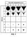
- Figure 1 schematically shows the cross-section of the beam at different distances from the (paraxial) focal plane, as calculated with computer simulations.
- the rows show the cross-sections at different degrees of defocus, and the columns show the sections at different values of 3 rd order astigmatism.
- the 2 nd row indicates the cross-sections of the beam in a plane which, viewed from the object lens, has been placed a certain distance behind the focal plane, whilst the 1 st row reproduces the cross-sections of the beam in a plane located at the same distance behind it.
- the 4 th and 5 th rows show cross-sections of the beam in planes which lie between the parallax focal plane and the object lens.
- the image of the sample is the convolution of the image that would be formed if the sample were to be scanned with a beam of infinitely small diameter and the actual diameter of the beam.
- a deconvolution of the image can then be carried out with the reconstructed shape of the sample, which gives a reconstruction of the beam diameter at a certain distance from the focus.
- the beam shape can be determined, whereupon the lens errors can be determined by intrinsically known methods.
- the excitation of the corrector can then be varied, manually or controlled by a computer, so that the lens errors are reduced. This process may be repeated several times, for example, until the lens errors are smaller than a pre-established value, or until the beam diameter in the focus has a value that is smaller than the pre-established value.
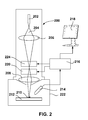
- Figure 2 schematically shows a device for implementing the method according to the invention.
- An electron column 200 such as an SEM (Scanning Electron Microscope) contains an electron source 202 which generates an electron beam 204.
- This electron beam 204 is focussed on a sample position 210 by lenses such as magnetic lenses, 206 and 208.
- This sample position 210 is placed on a displacement table 212 in order to move the area to be inspected from a sample to the focus of electron beam 204.
- Electron beam 204 is scanned over the surface of a sample placed in sample position 210 by deflector 220 under the control of a central control unit 216.
- SED secondary electron detector
- SED 214 The signal from SED 214 is transmitted to central control unit 216, which converts this spatially dependent signal to a signal for a monitor 218, whereupon the user obtains an image of the sample.
- SED 214, displacement table 212 and sample position 210 are located in a sample chamber 222. Both electron column 200 and sample chamber 222 are retained in a vacuum during operation of the device by evacuation means not shown.
- a corrector 224 which corrector contains a plurality of electrical and/or magnetic multipoles, for example, as is known to the person skilled in the art, is amplified by central control unit 216 for reducing the effect of lens errors caused by lens 206.
- a mono-crystal of magnesium oxide for example, is placed on a substrate of carbon or silicon in sample position 210.
- the correct excitation can be found for corrector 224.
- a sample to be examined can then be brought into the sample position, whereupon this sample can be examined.
Landscapes
- Chemical & Material Sciences (AREA)
- Analytical Chemistry (AREA)
- Analysing Materials By The Use Of Radiation (AREA)
Abstract
Description
- The invention relates to a method for determining lens errors in a particle-optical device, which device is designed to scan a sample with a focussed particle beam, comprising
- the supply of a sample with parts having a known shape,
- the production of one or more images of the sample by scanning the sample with the particle beam, and
- a determination of the cross-section of the beam on the basis of the image(s) produced.
- Samples for such a method are known from the catalogue "Scanning Electron Microscopy Supplies" from Canemco, (821B McCaffrey St., St. Laurent, (Montreal) Quebec, Canada. ).
- This method is used with particle-optical device such as the SEM (Scanning Electron Microscope), STEM (Scanning Transmission Electron Microscope) and FIB (Focused Ion Beam) devices.
- Particle-optical devices of the above-mentioned type are used, for example, in the semiconductor industry for the inspection, analysis and modification of samples.
- SEM and STEM devices are used for inspecting and analysing samples. Here a sample to be examined is scanned by a focussed particle beam. This particle beam is a beam of electrons, which beam is focussed on the sample with an object lens. The focus of the beam on the sample has a diameter of e.g. 1 nm. The beam is scanned over the sample, as a result of which (spatially dependent) information is released, e.g. in the form of secondary electrons. This information is detected and made available in the form of an image of the sample.
- FIB devices use a focussed ion beam which is scanned over the sample. The ion beam may cause the material of the sample to be etched away or the material to be merely deposited on the sample. The effect of the ion beam is also determined by the composition of the sample and by gases which are allowed in the vicinity of the sample. Moreover, (spatially dependent) information is released, e.g. in the form of secondary electrons. This information can be detected and can be made available in the form of an image of the sample.
- It should be pointed out that an electron beam can cause etching or deposition due to gases in the area surrounding the sample.
- Such devices frequently display astigmatism (or more precisely: astigmatism of the 1st order). In the case of astigmatism of the 1st order the beam has two mutually perpendicular line foci. One line focus may be represented on the sample by a slight under-focus of the object lens, and the other line focus can be represented on the sample by a slight over-focus of the object lens.
- Exactly between the line foci, where the focus of the beam is located, the resolution will be poorer than if there is no astigmatism, since the diameter of the beam is at least half the length of each of the line foci at that point.
- It should be pointed out that such devices are in most cases equipped with a corrector in the form of a stigmator for correcting the astigmatism, which stigmator brings the two line foci together so that a point focus is formed.
- In the method of prior art a sample is used in the form of tin balls on a carbon substrate in order to determine the presence of astigmatism. Such tin balls approach the ideal spherical shape to a large degree, as described in "An improved standard specimen for alignment of electron microscopes", K. R. Carson et al 1967 J. Sci. Instrum. 44 1036-1037, where a method is described for the manufacture of such samples.
- The tin ball form of prior art makes it possible, when they are viewed in a particle-optic device such as an electron microscope, to see easily whether the beam displays astigmatism. Due to the prior art shape of the tin balls a perfectly round image of the tin balls is expected, the sharpness of the edge of the image being the same throughout. However, for the orientations where the line focus touches the circumference of the tin ball tangentially, a sharp image will be obtained, but where the line focus touches the circumference of the tin ball radially, a lack of sharpness will occur, amounting to the length of the line focus. A sharp image is in this case understood to be an image with a resolution that is obtained without astigmatism.
- By now varying the excitation of the stigmator, whilst repeatedly focussing and slightly defocusing the object lens, until no further astigmatism can be shown, the astigmatism is corrected.
- One disadvantage of the tin balls of prior art is that the size according to the known catalogue is no smaller than 10 nm, whereas most tin balls have a much larger diameter. Where the resolution to be obtained is 1 nm, for example, as can today be achieved with an SEM, it is not easily possible to remove all astigmatism by means of such a sample.
- A further disadvantage of the tin balls of prior art is that they do not lend themselves well to determining other lens errors, e.g. astigmatism of the 3rd order or coma. These errors give rise to a cross-section of the beam (i.e. a section that is perpendicular to the optical axis of the lens) in which the magnification has a greater degree of symmetry than in the case of astigmatism of the 1st order. Astigmatism of the 3rd order, with a certain degree of under- and overfocus, for example, gives rise to a beam cross-section that is equal to a triangle, whilst the combination of spherical aberration and 3rd order astigmatism, even in focus, has a triangular cross-section. Consequently there will be no sharp image of a tin ball in any direction, which makes it difficult to determine the lens errors.
- An overview of beam diameters caused by different lens errors is given in "Erprobung eines sphärisch und chromatisch korrigierten Elektronenmikroskopes" (Testing of a spherically and chromatically corrected electron microscope), W. Bernard, Optik 57 (1980), pages 73-94, in particular page 83.
- It should be noted that the beam diameter of a beam which suffers from several errors is not necessarily a summation of the beam diameter of each of the errors. Spherical aberration and 3rd order astigmatism give rise, each separately in the focal plane, a rotation symmetrical beam diameter. However, as will be shown later in the figures, a combination of spherical aberration and 3rd order astigmatism in the focal plane, for example, gives rise to a beam diameter with a triangular cross-section.
- The object of the invention is to provide a method whereby the shape of the sample lends itself to more accurate determination of lens errors than the method of prior art.
- For this purpose the method according to the invention is characterised in that the sample is a crystalline sample with a free edge, which edge is formed by a mono-crystal.
- The invention is based on the realisation that the image of the sample is the convolution of an error-free image of the sample on the one hand and the actual diameter of the beam on the other. By now representing the sample parts with known angles and/or sharp edges, an accurate estimate can be made of the image as it should appear if it were to be represented with a beam having an ideal focus. This enables the shape of the beam to be determined by deconvolution, which in turn makes it possible to determine the lens errors.
A mono-crystal frequently has the required parts as sharp edges and known angles.. - An additional advantage is that consequently it is not so much the shape and size of the entire sample that is important, but rather that of only individual parts of the sample, for example the angles of the sample. It is therefore still possible to represent parts which have a radius of less than one nanometer with a sample having a dimension of over 10 nm, for example.
- It should be noted that it is possible to use samples which lie on a substrate of silicon or carbon, for example, but also samples which are partially embedded in a substrate, as well as samples in which parts of the sample lie free in relation to the substrate.
- It should also be noted that (arts of) mono-crystals are also understood to mean nanotubes and nanowires, for example, as described for instance by Guiton et al., J. Am. Chem. Soc. 127 (2005), pp 498-499.
- In an embodiment of the method according to the invention the crystalline sample is a mono-crystal.
- In this embodiment the entire sample is a mono-crystal, and all the sides and corners have the sides and corners that characterise a mono-crystal. If the image of the crystal is now viewed, the cross-section of the beam can be accurately established.
- In another embodiment of the method according to the invention, the mono-crystal has right angles.
- In a shape with right angles, slight out of roundness of the beam diameter will result in a clearly differentiated image of said angles. Very small deviations from the beam diameter can already be observed, particularly if such a sample is viewed perpendicular to a plane of the sample, the shape observed therefore being a rectangle.
- It should be noted that in order to have a shape with right angles, it is necessary for the mono-crystal to have a crystal lattice in which the angles of the lattice are right angles. Such crystal lattices are also referred to as tetragonal, ortho-rhombic or cubic. However, it is not the case that every mono-crystal with such a crystal lattice has a shape with right angles. A cubic mono-crystal may also have a hexagonal, tetrahedral or dodecahedral shape, for example.
- In a further embodiment of the method according to the invention the mono-crystal is a salt crystal.
- The image of a particle beam device is often produced on the basis of the quantity of secondary electrons that are released in response to the beam incident particles. The average quantity of secondary electrons which are released in response to one incident particle is known as the secondary emission coefficient.
When scanning with an electron beam, salt crystals frequently have a secondary emission coefficient > 2, from low beam energies of less than 200 eV to high beam energies of over 100 keV, for example. Commonly used substrates, such as carbon or silicon, have a low secondary emission coefficient at these different particular energies, so that a sharp contrast between sample and substrate is obtained. Salt crystals may therefore be used for a wide range of beam energies. - In yet another embodiment, the salt crystal consists of magnesium oxide.
- Magnesium oxide is a salt that can easily be formed, so that has crystal with right angles.
- A further advantage is that magnesium oxide mono-crystals of a small dimension can easily be formed on a substrate such as a silicon wafer by moving the wafer through the flame of a burning magnesium strip. In this case magnesium cubes and bars are formed which are aligned to the wafer surface: these are so-called "self-assembling structures". By selecting the incidence of the particle beam perpendicular to the substrate, only one plane will be represented as a result of this alignment, which plane is a right angle. This enables the beam shape to be determined relatively easily with the aid of computer techniques, for example. These samples therefore lend themselves to determining various errors of the beam, such as astigmatism of the 3rd order and coma.
- Another advantage of cubic crystals with such an orientation is that the lateral surfaces of the sample (i.e. the planes of the sample adjacent to the observed plane) are not exposed by the beam at all, so that the ribs that determine the aforementioned angles can be established very clearly.
- In yet another embodiment of the method according to the invention the mono-crystal has a maximum dimension of 100 nm.
- The use of so-called nanocrystals, by which are meant mono-crystals with a maximum dimension of less than 100 nm, for example, is attractive because the size of these mono-crystals does not differ by many orders of magnitude from the diameter of the beam with which the mono-crystal is scanned. It is therefore possible, with the reproduction techniques currently used, in which e.g. 1000*1000 pixels are represented, to represent the entire sample when at the same time the beam diameter occupies several pixels. The latter is necessary to be able to determine the beam shape with sufficient accuracy.
- In yet another embodiment of the method according to the invention, the sample is placed on a substrate, wherein the secondary emission coefficient of the substrate and sample differs considerably.
- It should be clear that it is necessary for the secondary emission coefficient of the substrate and sample to be different. Because of this substantial difference, a high contrast between the sample and substrate is achieved.
- In yet another embodiment of the method according to the invention the sample is placed on an electrically conducting material.
- Besides lens errors, charges of the sample may also give rise to distortion of the image. It would then be unclear whether the distortions are the result of charging or a result of lens errors. By now placing the sample on a conducting substrate, charging is prevented as much as possible.
- In yet another embodiment of the method according to the invention the particle optical device is provided with a corrector for lens errors, which corrector is amplified by means of the lens error determination obtained, so that the lens errors are reduced.
- The invention is now explained in further detail with reference to two figures, where:
- Figure 1 schematically shows the cross-section of the beam at different distances from the (paraxial) focal plane, as calculated with computer simulations, and
- Figure 2 schematically shows a device for implementing the method according to the invention.
- Figure 1 schematically shows the cross-section of the beam at different distances from the (paraxial) focal plane, as calculated with computer simulations.
- In this simulation the beam suffers in all cases from the same degree of spherical aberration. The rows show the cross-sections at different degrees of defocus, and the columns show the sections at different values of 3rd order astigmatism.
The focal plane is indicated in the 3rd row, at defocus=0. The 2nd row indicates the cross-sections of the beam in a plane which, viewed from the object lens, has been placed a certain distance behind the focal plane, whilst the 1st row reproduces the cross-sections of the beam in a plane located at the same distance behind it.
Similarly, the 4th and 5th rows show cross-sections of the beam in planes which lie between the parallax focal plane and the object lens. - In the 1st column, on the far left, no 3rd order astigmatism is present and the beam only suffers from spherical aberration. In the 2nd column, a certain degree of 3rd order astigmatism is present in addition to the same spherical aberration as is present in
column 1. In the 3rd column, in addition to the spherical aberration, 3rd order astigmatism is present which is twice as great as that in the 2nd column. In the 4th column, in addition to the spherical aberration, 3rd order astigmatism is present which is 3 times larger thant in the 2nd column. - As is known to the person skilled in the art, spherical aberration gives rise to a beam diameter which is rotation symmetrical about the axis of the lens. However, 3rd order astigmatism causes an asymmetrical beam diameter with a triple symmetry. It is clearly seen that as 3rd order astigmatism increases, so the beam diameter becomes increasingly less rotation symmetrical.
- By determining the beam shape for different defocus distances, it will be possible to determine the lens error with suitable metrics. Although spherical aberration and 3rd order astigmatism are used as lens errors in this example, it will be clear that other lens errors can also be determined in this way.
- As shown earlier, the image of the sample is the convolution of the image that would be formed if the sample were to be scanned with a beam of infinitely small diameter and the actual diameter of the beam. By determining the position and orientation of ribs of the sample structures, for example, on the basis of the image obtained (which is a convolution of the sample and the beam shape), the shape of the sample can be reconstructed.
- As is known to the person skilled in the art, a deconvolution of the image can then be carried out with the reconstructed shape of the sample, which gives a reconstruction of the beam diameter at a certain distance from the focus.
- By carrying out this reconstruction of the beam diameter at different defocuses, the beam shape can be determined, whereupon the lens errors can be determined by intrinsically known methods. The excitation of the corrector can then be varied, manually or controlled by a computer, so that the lens errors are reduced. This process may be repeated several times, for example, until the lens errors are smaller than a pre-established value, or until the beam diameter in the focus has a value that is smaller than the pre-established value.
- Figure 2schematically shows a device for implementing the method according to the invention.
- An
electron column 200, such as an SEM (Scanning Electron Microscope) contains anelectron source 202 which generates anelectron beam 204. Thiselectron beam 204 is focussed on asample position 210 by lenses such as magnetic lenses, 206 and 208. Thissample position 210 is placed on a displacement table 212 in order to move the area to be inspected from a sample to the focus ofelectron beam 204.Electron beam 204 is scanned over the surface of a sample placed insample position 210 bydeflector 220 under the control of acentral control unit 216. Whenelectron beam 204 is scanned over the sample placed insample position 210, secondary electrons are released which are detected by means of a secondary electron detector (SED) 214. These secondary electrons therefore provide spatially dependent information on the sample. The signal fromSED 214 is transmitted tocentral control unit 216, which converts this spatially dependent signal to a signal for amonitor 218, whereupon the user obtains an image of the sample.SED 214, displacement table 212 andsample position 210 are located in asample chamber 222. Bothelectron column 200 andsample chamber 222 are retained in a vacuum during operation of the device by evacuation means not shown. - A
corrector 224, which corrector contains a plurality of electrical and/or magnetic multipoles, for example, as is known to the person skilled in the art, is amplified bycentral control unit 216 for reducing the effect of lens errors caused bylens 206. - In order to establish the correct excitation for the
corrector 224, a mono-crystal of magnesium oxide, for example, is placed on a substrate of carbon or silicon insample position 210. By then carrying out the method according to the invention, the correct excitation can be found forcorrector 224. A sample to be examined can then be brought into the sample position, whereupon this sample can be examined.
Claims (9)
- A method for determining lens errors in a particle-optical apparatus, which apparatus is designed to scan a sample with a focussed particle beam, comprising• the supply of a sample with parts having a known shape,• the production of one or more images of the sample by scanning the sample with the particle beam, and• a determination of the cross-section of the beam on the basis of the image(s) produced,characterised in that• the sample is a crystalline sample with a free edge, which edge is formed by the edge of a mono-crystal.
- The method according to Claim 1, wherein the crystalline sample is a mono-crystal.
- The method according to any one of the preceding claims, wherein the mono-crystal has right angles.
- The method according to Claim 3, wherein the mono-crystal is a salt crystal.
- The method according to Claim 4, wherein the salt crystal is a mono-crystal of magnesium oxide.
- The method according to any one of the preceding claims, wherein the mono-crystal has a maximum dimension of 100 nm.
- The method according to any one of the preceding claims, wherein the sample is placed on a substrate, and wherein the secondary emission coefficients of the substrate and sample differ substantially.
- The method according to any one of the preceding claims, wherein the sample is placed on an electrically conducting substrate.
- The method according to any one of the preceding claims, wherein the particle optical apparatus is provided with a corrector for lens errors, which corrector is excited according to the determined cross-section of the beam, so that lens errors are reduced.
Applications Claiming Priority (1)
| Application Number | Priority Date | Filing Date | Title |
|---|---|---|---|
| NL1029847A NL1029847C2 (en) | 2005-09-01 | 2005-09-01 | Method for determining lens errors in a particle-optical device. |
Publications (2)
| Publication Number | Publication Date |
|---|---|
| EP1772894A2 true EP1772894A2 (en) | 2007-04-11 |
| EP1772894A3 EP1772894A3 (en) | 2008-12-17 |
Family
ID=36129736
Family Applications (1)
| Application Number | Title | Priority Date | Filing Date |
|---|---|---|---|
| EP06119848A Withdrawn EP1772894A3 (en) | 2005-09-01 | 2006-08-31 | Method for determining lens errors in a particle-optical device |
Country Status (5)
| Country | Link |
|---|---|
| US (1) | US7518121B2 (en) |
| EP (1) | EP1772894A3 (en) |
| JP (1) | JP2007066902A (en) |
| CN (1) | CN1924553B (en) |
| NL (1) | NL1029847C2 (en) |
Families Citing this family (15)
| Publication number | Priority date | Publication date | Assignee | Title |
|---|---|---|---|---|
| EP1783811A3 (en) * | 2005-11-02 | 2008-02-27 | FEI Company | Corrector for the correction of chromatic aberrations in a particle-optical apparatus |
| JP5243912B2 (en) * | 2008-01-24 | 2013-07-24 | 日本電子株式会社 | Beam position calibration method in charged particle beam apparatus |
| EP2166557A1 (en) * | 2008-09-22 | 2010-03-24 | FEI Company | Method for correcting distortions in a particle-optical apparatus |
| EP2197018A1 (en) * | 2008-12-12 | 2010-06-16 | FEI Company | Method for determining distortions in a particle-optical apparatus |
| US7884334B2 (en) * | 2009-01-22 | 2011-02-08 | Hermes Microvision, Inc. | Charged particle beam imaging method and system thereof |
| EP2471086B1 (en) * | 2009-08-28 | 2013-12-11 | FEI Company | Pattern modification schemes for improved fib patterning |
| EP2292953A1 (en) * | 2009-09-07 | 2011-03-09 | Fei Company | High-vacuum seal |
| EP2325862A1 (en) | 2009-11-18 | 2011-05-25 | Fei Company | Corrector for axial aberrations of a particle-optical lens |
| EP2511936B1 (en) | 2011-04-13 | 2013-10-02 | Fei Company | Distortion free stigmation of a TEM |
| EP2557584A1 (en) * | 2011-08-10 | 2013-02-13 | Fei Company | Charged-particle microscopy imaging method |
| EP2722566B1 (en) | 2012-10-19 | 2015-05-13 | Fei Company | Coated O-ring |
| US9928989B2 (en) * | 2014-07-22 | 2018-03-27 | Intelligent Virus Imaging Inc. | Method for automatic correction of astigmatism |
| US9978557B2 (en) | 2016-04-21 | 2018-05-22 | Fei Company | System for orienting a sample using a diffraction pattern |
| US10790114B2 (en) * | 2017-06-29 | 2020-09-29 | Kla-Tencor Corporation | Scanning electron microscope objective lens calibration using X-Y voltages iteratively determined from images obtained using said voltages |
| US11810753B2 (en) * | 2021-10-13 | 2023-11-07 | ICT Integrated Circuit Testing Gesellschaft für Halbleiterprüftechnik mbH | Methods of determining aberrations of a charged particle beam, and charged particle beam system |
Family Cites Families (9)
| Publication number | Priority date | Publication date | Assignee | Title |
|---|---|---|---|---|
| DE2535510C2 (en) * | 1975-08-06 | 1977-09-08 | Siemens AG, 1000 Berlin und 8000 München | Electron beam scanning device for structural analysis of specimens |
| US4144488A (en) * | 1977-12-22 | 1979-03-13 | The United States Of America As Represented By The Secretary Of The Navy | Investigation of near-surface electronic properties in semiconductors by electron beam scanning |
| US4200794A (en) * | 1978-11-08 | 1980-04-29 | Control Data Corporation | Micro lens array and micro deflector assembly for fly's eye electron beam tubes using silicon components and techniques of fabrication and assembly |
| US4444744A (en) * | 1980-03-03 | 1984-04-24 | Goldenberg Milton David | Tumor localization and therapy with labeled antibodies to cell surface antigens |
| DE3008260A1 (en) * | 1980-03-04 | 1981-09-17 | Siemens AG, 1000 Berlin und 8000 München | METHOD FOR RECORDING FLOW LIMIT LAYERS IN LIQUID MEDIA |
| US6426501B1 (en) | 1998-05-27 | 2002-07-30 | Jeol Ltd. | Defect-review SEM, reference sample for adjustment thereof, method for adjustment thereof, and method of inspecting contact holes |
| US6544463B1 (en) * | 1999-07-26 | 2003-04-08 | The Trustees Of The University Of Pennsylvania | Hybrid materials and methods for producing the same |
| NL1022855C2 (en) * | 2003-03-05 | 2004-09-07 | Univ Delft Tech | Method and device for the controlled manufacture of openings on a nanometer scale. |
| US7164128B2 (en) | 2003-11-25 | 2007-01-16 | Hitachi High-Technologies Corporation | Method and apparatus for observing a specimen |
-
2005
- 2005-09-01 NL NL1029847A patent/NL1029847C2/en not_active IP Right Cessation
-
2006
- 2006-08-29 JP JP2006232398A patent/JP2007066902A/en not_active Withdrawn
- 2006-08-30 US US11/512,806 patent/US7518121B2/en active Active
- 2006-08-31 EP EP06119848A patent/EP1772894A3/en not_active Withdrawn
- 2006-08-31 CN CN200610126647.4A patent/CN1924553B/en not_active Expired - Fee Related
Also Published As
| Publication number | Publication date |
|---|---|
| CN1924553A (en) | 2007-03-07 |
| CN1924553B (en) | 2013-01-02 |
| US20070045558A1 (en) | 2007-03-01 |
| EP1772894A3 (en) | 2008-12-17 |
| NL1029847C2 (en) | 2007-03-05 |
| JP2007066902A (en) | 2007-03-15 |
| US7518121B2 (en) | 2009-04-14 |
Similar Documents
| Publication | Publication Date | Title |
|---|---|---|
| US7518121B2 (en) | Method for determining lens errors in a particle-optical device | |
| US9029767B2 (en) | Method for adjusting a stem equipped with an aberration corrector | |
| TWI488212B (en) | Arrangement and method for the contrast improvement in a charged particle beam device for inspecting a specimen | |
| TWI747099B (en) | Charged particle beam systems, dispersion devices for the charged particle beam systems, and methods for controlling dispersion in the charged particle beam systems | |
| US8294096B2 (en) | Charged particle beam device and a method of operating a charged particle beam device | |
| JP2019053976A (en) | Charged particle beam device, charged particle beam influencing device, and method of operating charged particle beam device | |
| TWI749498B (en) | Method and apparatus for determining a wavefront of a massive particle beam | |
| US8164067B2 (en) | Arrangement and method for the contrast improvement in a charged particle beam device for inspecting a specimen | |
| TWI673749B (en) | High resolution charged particle beam device and method of operating the same | |
| EP1648018B1 (en) | Focussing lens and charged particle beam device for non zero landing angle operation | |
| CN117672786A (en) | Magnetic multipole devices, charged particle beam devices and methods of influencing charged particle beams propagating along an optical axis | |
| TWI761656B (en) | Electron beam apparatus and methods of reducing thermal induced beam drift in an electron beam | |
| TW202431319A (en) | Method of determining a brightness of a charged particle beam, method of determining a size of a source of the charged particle beam, and charged particle beam imaging device | |
| JP2004319149A (en) | Electron source and electron beam device using the same | |
| Lutsch et al. | Initial resolution measurements of miniaturized electrostatic lenses for LVSEM | |
| US12412727B2 (en) | Charged particle beam system, corrector for aberration correction of a charged particle beam, and method thereof | |
| JP2019519063A (en) | Method of manufacturing monochromator | |
| US12451322B2 (en) | Method of forming a multipole device, method of influencing an electron beam, and multipole device | |
| TW202447685A (en) | Method of determining an energy spectrum or energy width of a charged particle beam, and charged particle beam imaging device | |
| Barragán Sanz | Implementation and Improvement of Metal-Film Phase Plates for Single-Particle Cryo-EM | |
| Hetherington et al. | Aberration-corrected HREM/STEM for semiconductor research | |
| WO2023061651A1 (en) | Methods of determining aberrations of a charged particle beam, and charged particle beam system |
Legal Events
| Date | Code | Title | Description |
|---|---|---|---|
| PUAI | Public reference made under article 153(3) epc to a published international application that has entered the european phase |
Free format text: ORIGINAL CODE: 0009012 |
|
| AK | Designated contracting states |
Kind code of ref document: A2 Designated state(s): AT BE BG CH CY CZ DE DK EE ES FI FR GB GR HU IE IS IT LI LT LU LV MC NL PL PT RO SE SI SK TR |
|
| AX | Request for extension of the european patent |
Extension state: AL BA HR MK YU |
|
| PUAL | Search report despatched |
Free format text: ORIGINAL CODE: 0009013 |
|
| AK | Designated contracting states |
Kind code of ref document: A3 Designated state(s): AT BE BG CH CY CZ DE DK EE ES FI FR GB GR HU IE IS IT LI LT LU LV MC NL PL PT RO SE SI SK TR |
|
| AX | Request for extension of the european patent |
Extension state: AL BA HR MK RS |
|
| AKX | Designation fees paid |
Designated state(s): DE FR GB |
|
| STAA | Information on the status of an ep patent application or granted ep patent |
Free format text: STATUS: THE APPLICATION IS DEEMED TO BE WITHDRAWN |
|
| 18D | Application deemed to be withdrawn |
Effective date: 20090618 |