EP1771810B1 - System, circuit, and method for edge detection in a binary optical code - Google Patents
System, circuit, and method for edge detection in a binary optical code Download PDFInfo
- Publication number
- EP1771810B1 EP1771810B1 EP05765457.6A EP05765457A EP1771810B1 EP 1771810 B1 EP1771810 B1 EP 1771810B1 EP 05765457 A EP05765457 A EP 05765457A EP 1771810 B1 EP1771810 B1 EP 1771810B1
- Authority
- EP
- European Patent Office
- Prior art keywords
- derivative
- peak
- signal
- peaks
- circuit
- Prior art date
- Legal status (The legal status is an assumption and is not a legal conclusion. Google has not performed a legal analysis and makes no representation as to the accuracy of the status listed.)
- Expired - Lifetime
Links
Images





Classifications
-
- G—PHYSICS
- G06—COMPUTING OR CALCULATING; COUNTING
- G06K—GRAPHICAL DATA READING; PRESENTATION OF DATA; RECORD CARRIERS; HANDLING RECORD CARRIERS
- G06K7/00—Methods or arrangements for sensing record carriers, e.g. for reading patterns
- G06K7/10—Methods or arrangements for sensing record carriers, e.g. for reading patterns by electromagnetic radiation, e.g. optical sensing; by corpuscular radiation
- G06K7/10544—Methods or arrangements for sensing record carriers, e.g. for reading patterns by electromagnetic radiation, e.g. optical sensing; by corpuscular radiation by scanning of the records by radiation in the optical part of the electromagnetic spectrum
- G06K7/10821—Methods or arrangements for sensing record carriers, e.g. for reading patterns by electromagnetic radiation, e.g. optical sensing; by corpuscular radiation by scanning of the records by radiation in the optical part of the electromagnetic spectrum further details of bar or optical code scanning devices
- G06K7/10851—Circuits for pulse shaping, amplifying, eliminating noise signals, checking the function of the sensing device
-
- G—PHYSICS
- G06—COMPUTING OR CALCULATING; COUNTING
- G06K—GRAPHICAL DATA READING; PRESENTATION OF DATA; RECORD CARRIERS; HANDLING RECORD CARRIERS
- G06K7/00—Methods or arrangements for sensing record carriers, e.g. for reading patterns
- G06K7/10—Methods or arrangements for sensing record carriers, e.g. for reading patterns by electromagnetic radiation, e.g. optical sensing; by corpuscular radiation
- G06K7/14—Methods or arrangements for sensing record carriers, e.g. for reading patterns by electromagnetic radiation, e.g. optical sensing; by corpuscular radiation using light without selection of wavelength, e.g. sensing reflected white light
-
- G—PHYSICS
- G06—COMPUTING OR CALCULATING; COUNTING
- G06K—GRAPHICAL DATA READING; PRESENTATION OF DATA; RECORD CARRIERS; HANDLING RECORD CARRIERS
- G06K7/00—Methods or arrangements for sensing record carriers, e.g. for reading patterns
- G06K7/10—Methods or arrangements for sensing record carriers, e.g. for reading patterns by electromagnetic radiation, e.g. optical sensing; by corpuscular radiation
- G06K7/14—Methods or arrangements for sensing record carriers, e.g. for reading patterns by electromagnetic radiation, e.g. optical sensing; by corpuscular radiation using light without selection of wavelength, e.g. sensing reflected white light
- G06K7/1404—Methods for optical code recognition
- G06K7/1439—Methods for optical code recognition including a method step for retrieval of the optical code
- G06K7/1452—Methods for optical code recognition including a method step for retrieval of the optical code detecting bar code edges
-
- G—PHYSICS
- G06—COMPUTING OR CALCULATING; COUNTING
- G06V—IMAGE OR VIDEO RECOGNITION OR UNDERSTANDING
- G06V10/00—Arrangements for image or video recognition or understanding
- G06V10/20—Image preprocessing
- G06V10/28—Quantising the image, e.g. histogram thresholding for discrimination between background and foreground patterns
Definitions
- optical code readers such as, for example, bar code readers, and more particularly to signal processing techniques and circuitry for determining edge positions in a binary optical code.
- a bar code typically serves as an identifier of an object, whether the identification be to a class of objects (e.g., oranges) or a unique item (e.g., U.S. Patent No. 6,012,639 ).
- US 6,499,662 B1 discloses a method for improving the accuracy of edge detection and EP 0745951 A2 and US 6,209,788 B1 show different optical scanner.
- Figure 1A depicts a segment of a typical bar code 100, with alternating bars (i.e..
- the positions of the bars 102 and spaces 104 encode particular information. More specifically, the widths of the bars 102 and spaces 104 are often set to encode a desired information sequence, as the pattern of bars and spaces represents a string of binary ones and zeros, wherein the width of any particular bar or space is an integer multiple of a specified minimum width, which is called a "module" or "unit.” Thus, to decode the information, a bar code reader must be able to reliably discern the edge locations of the bars 102 and the spaces 104.
- the leading edge of a bar i.e., a light-to-dark transition
- an STV set video
- the trailing edge of a bar i.e., a dark-to-light transition
- RTV reset video
- the first several STVs and RTVs of the bar code 100 are labeled in Figure 1A . assuming (arbitrarily) that the bar code is scanned from left to right.
- Optical scanning equipment can be utilized to generate an electrical signal indicative of the positions of bars and spaces in a bar code.
- a signal denoted x(t)
- x(t) is depicted in simplified form in Figure 1B for the corresponding bar code 100.
- Typical optical scanning equipment comprises one or more illumination sources and one or more photodetectors.
- the illumination source may be a laser producing a focused beam spot on a small area of the bar code 100.
- a photodetector detects the laser light reflected off the bar code 100 and produces an electrical signal whose magnitude is related to the optical power of the reflected signal.
- the photodetector generates an electrical signal whose variations over time at least roughly correlate to the spatial pattern of bars 102 and spaces 104 in the bar code 100.
- the illumination source may be diffuse across the entire bar code 100, and the bar code may be imaged using a charge-coupled device (CCD) camera or a CMOS (complementary metal-oxide-semiconductor) imager, either of which forms an electronic image of the bar code 100.
- That electronic image can be sampled in the forward direction of the bar code 100 to generate a virtual scan line signal, much like the scan line signal generated with a scanning laser spot.
- the result is an electronic signal, which, at least ideally, somehow relates to the spatial positions of the bars 102 and spaces 104 in the bar code 100.
- the next step is to process that signal to determine with some reliability where the edges (STVs and RTVs) lie.
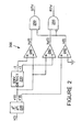
- FIG 2 is schematic diagram of a conventional edge detection system 200 for processing the scan line signal x(t) illustrated in Figure 1B .
- the system 200 performs edge detection using a typical gated peak detection scheme.
- the system 200 operates by forming the first and second derivatives of the scan line signal x(t) and by detecting zero crossings of the second derivative, which ideally represent optical edges.
- the system 200 qualifies zero crossings of the second derivative only if the first derivative exceeds a threshold.
- the system 200 includes a double differentiator 220, an envelope detector 230, three comparators 240, 242, and 246, and two logical AND gates 250 and 255.
- a preamplifier may amplify, buffer, invert and/or condition the scan line signal x(t), which is received at the input of the differentiator 220.
- the differentiator 220 produces a first derivative signal x'(t) and second derivative signal x"(t), respectively. While it is also possible to generate the first and second derivative signals x'(t) and x"(t) using two separate single differentiators, it is preferable to use common hardware to produce both to ensure more easily that x'(t) are x"(t) are time-aligned, as described in U.S. Patent No. 6,073,849 .
- the envelope detector 230 processes the first derivative signal x'(t) to determine, based on the extreme maximum and minimum values of that signal, a threshold value T somewhat smaller in magnitude than those extreme values.
- a suitable implementation of the envelope detector 230 is disclosed in U.S.Patent No.4,000,397 .
- the comparators 240 and 242 detect peaks in that signal and produce respective logical true-valued outputs y S (t) and y R (t) when the first derivative signal x'(t) exceeds the threshold value.
- y S (t) and y R (t) should be a logical true value during such peaks (y S (t) being true during a minimum or negative peak, and y R (t) being true during a maximum or positive peak). Because the second derivative signal should cross zero at such peaks, the comparator 246 is configured to detect those zero crossings and enable the appropriate AND gate 250 or 255, respectively, to generate the STV or RTV signal, such that only one of which is true at any given time.
- Figure 1B is a plot of the scan line signal x(t), which is derived from a photodetector current, which is generally at a higher value during the spaces 104 and a lower value during the bars 102, as more light is reflected from the spaces 104 than the bars 102. (Depending upon the optical scanning equipment, that relationship may be reversed.) However, the scan line signal x(t) is not a perfect representation of the bar code 100 for a variety of reasons discussed below.
- Figure 1C is a plot of the first derivative signal x'(t), including the threshold levels +T and -T.
- Figure 1D is the second derivative signal x"(t), which, as one can see, crosses zero whenever the first derivative signal x'(t) is at a peak.
- Figure 1E shows the signal y S (t), the output of the comparator 240. As can be seen, assuming high-true logic levels, as utilized in this figure, y S (t) is high when x'(t) ⁇ -T.
- Figure 1F shows the signal y R (t), the output of the comparator 242, which is high when x'(t) > +T.
- Figures 1G and 1H are plots of the RTV and STV signals, respectively, which are the logical AND combination of y R (t) and the condition that x"(t) ⁇ 0, and y S (t) and the condition that x"(t) > 0.
- the STV and RTV signals may contain multiple pulses for a single transition in the bar code 100 and thus do not unambiguously indicate edge positions in the bar code 100. This is due to the fact that more than one peak can occur in the first derivative signal x'(t) for a single real edge in the bar code 100 - a phenomenon that can be called "peak multiplication.” There are several reasons why more than one peak may appear in x'(t) for a given real transition edge. Some reasons are attributable to the optical scanner. For example, the spot profile of the laser beam may have multiple peaks. Another reason may be noise introduced by the optical scanner or the electronic circuitry.
- each local first derivative peak is detected as a separate like edge by the system 200.
- STV or RTV multiple adjacent edges of the same type (STV or RTV) cannot be legitimate, as adjacent edges must be of alternating types. Only one edge in such a group is the best estimate of the true edge position.
- edge detection techniques suffer from the same problem.
- multi-bit digitizers such as the systems disclosed in U.S. Patent Nos. 5,302,813 , 5,449,893 , and 5,734,152 , which operate by digitizing the first derivative peaks for an entire scan line and then applying various thresholds to the entire digitized record until a decodable peak pattern results, perform poorly in the presence of ISI (inter-symbol interference), which can result, for example, from the laser spot size being large compared to the unit width, and do not inherently ensure that multiple adjacent edges are rejected.
- ISI inter-symbol interference
- Bar codes are just one example of the many types of optical codes in use today.
- optical codes encode useful, optically-readable information about the items to which they are attached or otherwise associated. While bar codes generally encode information across one dimension, higher-dimensional optical codes are also possible, such as, two-dimensional matrix codes (e.g., MaxiCode) or stacked codes (e.g., PDF 417).
- two-dimensional matrix codes e.g., MaxiCode
- stacked codes e.g., PDF 417
- the present invention is directed to methods, according to claims 1 to 10 and circuits according to claims 10 to 17 for detecting transitions in a binary optical code signal, and thus detecting edges in a binary optical code.
- FIG. 3A is a block diagram of an edge detection system 300, according to one embodiment.
- the system 300 like the conventional system 200, operates according to a gated peak detection scheme, whereby zero crossings of the second derivative signal x"(t) are detected and qualified based on the amplitude of the first derivative signal x'(t).
- the differentiator 220; envelope detector 230; comparators 240, 242, and 246; and AND gates 250 and 255 can be the same hardware components as in the conventional system 200.
- the gated peak signals y S (t) and y R (t) represent in digital form the locations of local maxima and minima, respectively, in the first derivative signal x'(t), just as in the conventional system 200.
- the output of the comparator 246, the second derivative polarity signal u(t), is high when x"(t) is positive (i.e., when x'(t) is increasing) or low when x"(t) is negative (i.e., when x'(t) is decreasing).
- second derivative zero crossings indicated by transitions in u(t), indicate possible edge positions on the target label.
- the system 300 differs from the conventional system 200, however, in the way in which the zero crossings of the second derivative signal x"(t) are qualified to determine the most likely edge position.
- the system 300 unlike the conventional system 200, includes a multiple peak processing circuit 310, which rejects spurious peaks in the first derivative signal x'(t), as described in greater detail below.
- the outputs of the multiple peak processing circuit 310 are peak qualifying signals z S (t) and z R (t), which the system 300 processes just as the conventional system 200 processes the signals y S (t) and y R (t) to qualify zero crossings of the second derivative signal x"(t).
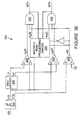
- FIG. 3B is a block diagram of an alternative edge detection system 305, according to another embodiment.
- the system 305 differs from the system 300 by use of a different multiple peak processing circuit 320, which rejects spurious peaks in the first derivative signal x'(t), as described in greater detail below.
- the outputs of the multiple peak processing circuit 320 are peak qualifying signals w S (t) and w R (t), which the system 305 utilizes in conjunction with the signals y S (t) and y R (t) to qualify zero crossings of the second derivative signal x"(t).
- the signals y S (t), w S (t), and u(t) are input to an AND gate 252, the output of which is an STV signal, and the signals y R (t), w R (t), and u(t) are input to an AND gate 256, the output of which is an RTV signal.
- FIG. 4 is a flowchart of a method 400 performed by, for example, the systems 300 or 305.
- the method 400 begins by generating (step 410) a scan line signal x(t) and differentiating (step 420) that signal.
- the method 400 detects (step 430) peaks in the first derivative signal x'(t).
- the output of the detecting step 430 is, in general, for each actual bar code edge, a series of successive like-polarity peaks, such as represented by the gated peak signals y S (t) and y R (t).
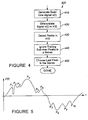
- peak p 4 is the maximum peak in the first group and therefore the most likely one representing the true edge location.
- a number of spurious leading peaks (p 1 , p 2 , and p 3 ) and trailing peaks (p 5 and P6 ) are also present in the first group.
- the method 400 ignores or discards the spurious peaks and chooses the maximum peak p 4 in two steps.
- the first step is ignoring (step 440) any trailing peaks less than the maximum peak so far encountered.
- the second step is choosing (step 450) the last remaining peak in the series.
- the ignoring step 440 first observes peak p 1 , which it does not discard. So far, peak p 1 is the maximum peak encountered. Next, the ignoring step 440 observes peak p 2 and does not discard it because, although it trails peak p 1 , it is not less than p 1 . Peak p 2 now becomes the maximum peak encountered. Next, the ignoring step 440 observes peak p 3 , which it discards as being less than the maximum at this point (which remains p 2 ). Next, the ignoring step 440 observes peak p 4 , which it does not discard and which becomes the new maximum peak.
- the ignoring step 440 observes peaks p 5 and p 6 , which it discards as being less than peak p 4 .
- the result of the ignoring step 440 is that peaks p 3 , p 5 , and p 6 are discarded, while only peaks p 1 , p 2 , and p 4 are passed to the choosing step 450.
- the choosing step 450 then chooses peak p 4 as the last-in-time peak in the group of non-discarded peaks.
- the method 400 thus arrives at the peak in the series having the greatest amplitude, which most likely represents the true edge position.
- the multiple peak processing circuits 310 or 320 can perform either the ignoring step 440 or both the ignoring step 440 and the choosing step 450.
- the choosing step 450 may be performed either before or after the AND gates 250 and 255 ( Figure 3A ) or the AND gates 252 and 256 ( Figure 3B ).
- a microcontroller implementation of the choosing step 450 is described fully in the above-referenced U.S. Patent No. 6,012,639 (see, in particular, the microcontroller 430). Other implementations are possible to achieve the same functionality.
- the ignoring step 440 may be implemented in electronic hardware as set forth, for example, in Figures 6A and 6B , which are schematic diagrams of circuits 600 and 605, representing one implementation of one half of the multiple peak processing circuits 310 and 320 in the edge detection systems 300 and 305, respectively.
- the circuits 600 and 605 are presented as the circuitry for processing just the positive peaks.
- the circuits 600 and 605 can easily be modified to also operate with an input signal of the opposite polarity; alternatively, circuits similar to the circuits 600 or 605 can easily be constructed to process just the negative peaks.
- the circuit 600 operates as follows: The first derivative signal x'(t) is connected to the gate of a transistor M 1 . When x'(t) is positive and increasing, the transistor M 1 turns on and conducts across its source and drain. The turn-on of the transistor M 1 has two effects. First, the same currents flow across each of transistors M 2 and M 3 , which form a current mirror. Second, that current charges a capacitor C 1 , as the transistor M 1 and the capacitor C 1 form a simple peak rectifier, and the voltage at the node 610 is a peak-rectified version of x'(t).
- the transistor M 4 is set to have a drain-to-source current equal to I REF /3, while a transistor M 5 is connected between the node 620 and ground, which supplies a drain-to-source current equal to I REF . That is accomplished by use of a transistor M 13 , which forms a current mirror with the transistors M 4 an M 5 .
- the transistors M 5 and M 13 are preferably designed to have a channel width-to-length ratio three times that of the transistor M 4 , so that the drain-to-source current through each of the transistor M 5 and M 13 is three times that of transistor M 4 .
- I REF the current through transistor M 5 , which discharges the node 620.
- I REF the current through transistor M 5 , which discharges the node 620.
- the initial decay rate of the voltage at the node 620 (after x"(t) ⁇ 2I REF /3C 1 but before the capacitor C 1 stops charging) should be carefully selected. If the initial decay rate is too fast, then the voltage at the node 620 will decay to ground before x"(t) crosses zero, and no edges will be rendered. If the initial decay rate is too slow, then the gate will remain open and qualify trailing peaks which are near in time to the peak having maximum amplitude. For a given system, the reference current I REF is therefore ideally chosen to ensure that all legitimate edges are rendered while still rejecting as many trailing peaks as possible.
- the transistor M 4 provides a small DC current to overcome whatever leakage current may flow in the transistors M 1 and M 2 . Without the current from M 4 , the leakage current from the transistors M 1 and M 2 would be integrated by the capacitor C 1 , causing the voltage at the node 610 to increase to near V DD . Thus, the current in M 4 should be chosen to be greater than the maximum possible leakage current through the transistors M 1 and M 2 . If the current through M 4 is too large, on the other hand, the gate-to-source voltage drop of M 1 could become large enough to limit dynamic range, especially if the supply voltage V DD is low.
- i(M 4 ) must be significantly smaller than i(M 5 ) to ensure that the voltage at the node 620 drops quickly to ground after the first derivative slope drops below the threshold.
- baseline noise can cause the voltage at the node 620 to qualify illegitimate edges.
- the voltage at the node 620 is qualified by AND-ing it with the gated peak signal y R (t), which is true when x'(t) exceeds a threshold generated conventionally (as in U.S. Patent No. 4,000,397 ).
- the logical AND-ing of these two signals occurs at an AND gate 625, as shown in Figure 6A .
- Figure 7 is a set of voltage-versus-time plots for various signals in the circuit 600.
- Figure 7A is a plot of a portion of x'(t), just as in Figure 5 , and a plot of the voltage v 610 (t) across the capacitor C 1 at the node 610. While x'(t) is initially rising, the capacitor C 1 is charging, and the voltage v 610 (t) tracks x'(t) except for a small voltage drop V GSM1 across the transistor M 1 . However, when x'(t) reaches a peak and begins falling, then the capacitor no longer charges and in fact begins discharging slowly due to the current in M 4 , until x'(t) exceeds the voltage v 610 (t) + V GSM1 again.
- the voltage v 610 (t) is a peak-rectified version of x'(t).
- Figure 7A also shows the threshold +T, which is applied to the generation of the signal y R (t).
- Figure 7B is a plot of x"(t), the derivative of x'(t).
- Figure 7B is the threshold level 2I REF /3C 1 .
- Figure 7C is a plot of the voltage v 620 (t) at the node 620. As explained above, the voltage v 620 (t) is at a high value when x"(t) exceeds the threshold level 21 REF /3C 1 . Otherwise, the voltage V 620 decays as shown.
- Figure 7D is a plot of y R (t), assuming the threshold shown in Figure 7A.
- Figure 7E is a plot of z R (t), which is the logical AND-ing of the voltage V 620 and y R (t).
- z R (t) contains pulses corresponding to the peaks p 1 , p 2 , and p 4 , but not the trailing sub-maximum peaks p 3 , p 5 , and p 6 .
- the circuit 605 comprises a comparator 630, an optional AND gate 635, a resistor R s , a transistor M S , and a capacitor C S , which together form a peak detector 638.
- the peak detector 638 detects peaks in the first derivative signal x'(t) as follows: Ignoring for the moment the AND gate 635 (or assuming for the moment that u(t) is high, meaning that x'(t) is rising), then the node 640, which is connected to the gate of the transistor M S , is high and therefore turns on the transistor M S whenever the first derivative signal x'(t) exceeds the voltage across the capacitor C S at the node 645.
- the first derivative signal x'(t) is connected to the node 645 across the resistor R s , causing the voltage at the node 645 to track the first derivative signal x'(t).
- the accumulated charge on the capacitor C s causes the voltage at the node 645 to be greater than the first derivative signal x'(t), causing the comparator 630 output to go low, which causes the voltage at the node 640 to go low, which in turn causes the transistor M S to turn off.
- the capacitor C S holds its accumulated charge and the voltage of the node 645 remains essentially constant unless and until the first derivative signal x'(t) exceeds the voltage at the node 645.
- the peak detector 638 tracks the first derivative signal x'(t) while it is increasing beyond a previous peak, or holds at a peak value until that peak value is again exceeded.
- the peak detector 638 would track to and thereafter hold at the maximum peak p 4 , as shown in simplistic form in Figure 8A .
- transistor M S is illustrated as a field-effect transistor (FET), it may be of any type of switching transistor or other suitable switch.
- the transistor M S functions as a switch, where the gate terminal is a control terminal controlling whether there is conduction between controllable conduction terminals, viz., the drain and source terminals.
- the peak detector 638 differs from a conventional peak detector; which typically would connect the drain terminal of the transistor M S to a positive supply voltage.
- An advantage of the peak detector in the circuit 605 is that it exhibits significantly less overshoot than the conventional implementation. That advantage can be important when processing high bandwidth signals, as often occurs in bar code reading. Overshoot occurs when the comparator 630 has a non-zero propagation delay that delays turn off of the transistor M S . If, as in the conventional peak detector, the drain terminal of the transistor M S were connected to a positive supply voltage, then significant additional charge could accumulate on the capacitor C s during that slight delay time.
- the parameters of the capacitor C S , the resistor R S , and the transistor M S are preferably chosen to satisfy application-specific constraints, such as input signal bandwidth, available circuitry area, and tolerable charge injection.
- application-specific constraints such as input signal bandwidth, available circuitry area, and tolerable charge injection.
- the time constant resulting from the product of C s and R s should be sufficiently small to permit the circuit to respond to variations in the input signal.
- charge injection becomes more problematic as the size of the capacitor C S decreases, and as the size of transistor M S increases. If the capacitance gets too large, it can affect the stability of the amplifier providing the input signal; resistor R S should therefore be large enough to isolate the amplifier output from this capacitance while in the tracking mode.
- the AND gate 635 is an optional component in the circuit 605. If included, as shown in Figure 6B , it can hasten the turn-off of the transistor M S , as the second derivative polarity signal u(t) tends to become negative earlier than the comparator 630 recognizes that a peak has been reached.
- One reason that the comparator 630 has a non-zero response time during transitions of its inputs is that the comparator 630 has a finite gain and has limited overdrive when its inputs are nearly equal, as is the case during transitions from tracking to holding modes at or near the peaks of the input signal.
- FIG. 6B Not shown in Figure 6B is reset circuitry to short the capacitor C S at the conclusion of a half-cycle. Such reset circuitry is illustrated in Figure 10 , which is discussed below.
- Figure 8B illustrates a more realistic plot of the behavior of the peak detector portion of the circuit 605 than the simplified one in Figure 8A .
- the Figure 8B plot was generated by computer simulation of the circuit 605 for a case in which the signal strength is quite small (in fact, near the lower limit to acceptably read bar codes).
- the voltage at the node 645 is generally slightly less than the first derivative signal x'(t). That tracking error becomes less significant as the signal strength increases and in fact is negligible at typical signal strength.
- Figure 7B also illustrates some pedestal error in the voltage at the node 645.
- the pedestal error is due, in part, to overshoot attributable to finite response time by the comparator 630.
- the pedestal error is also due, in part, to charge injection in the transistor M S .
- the circuit 605 also comprises a set-reset flip-flop 650.
- the node 640 is connected to the set input of the flip-flop 650, while the STV signal is connected to the reset input of the flip-flop 650.
- the operation of the flip-flop 650 can be understood by considering the signals depicted in Figure 8B .
- the peak detector 638 is in its tracking mode and the voltage at node 640 is high. This state is shown initially in Figure 8B from about 30 ⁇ s to about 31 ⁇ s.
- the high value at the node 640 sets the flip-flop 650, causing the signal w S (t) output from the flip-flop 650 to be high.
- the signals w S (t), y S (t) and u(t) are all high, causing the STV signal to be asserted.
- the STV signal then resets the flip-flop 650.
- x'(t) begins to decrease after the first peak, the peak detector enters its holding mode, and the voltage at the node 640 is low, in which case the flip-flop 650 remains reset and w S (t) remains low. That condition continues until x'(t) increases again and surpasses its previous peak (occurring somewhat after about 32 ⁇ s in Figure 8B ), at which point the peak detector 638 switches to its tracking mode, causing the flip-flop 650 to set.
- the STV signal is again asserted briefly until the flip-flop 650 is reset. This process repeats every time x'(t) rises to a peak of greater magnitude than any previous peak during a half-cycle.
- the STV signal is asserted near the peaks p 1 , p 2 , and p 4 , but not the peaks p 3 , p 5 , and p 6 .
- subsequent processing detects the last one p 4 , which is the maximum and best choice among the multiple peaks in the half cycle.
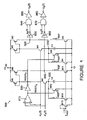
- Figure 9 and 10 are schematic diagrams of illustrative circuits 800 and 805 implementing both halves (STV and RTV) of the multiple peak processing circuit 310 and 320, respectively.
- the first derivative signal x'(t) is a differential signal.
- the two signals making up the differential pair are x' P (t) and x' N (t), the positive and negative sides, respectively.
- the circuit 800 contains two separate circuits, each like the circuit 600, one for each signal of the differential pair.
- the first circuit, which processes x' P (t) comprises the transistors M 1 - M 5 , capacitor C 1 , and the nodes 610 and 620, just as in the circuit 600.
- the other circuit, which processes x' N (t) comprises transistors M 7 - M 11 , a capacitor C 2 , and nodes 630 and 640 in the same configuration as the transistors M 1 - M 5 , the capacitor C 1 , and the nodes 610 and 620, respectively.
- the circuit 800 comprises additional circuitry to selectively enable and disable the two circuits such that only one operates at any given time.
- That additional circuitry comprises a comparator 810, an inverter 820, and two transistors M 6 and M 12 .
- the inputs of the comparator 810 are the differential pair x' P (t) and x' N (t).
- the output of the comparator 810 is a signal labeled RESET N , which is input to the inverter 820 to produce a signal labeled RESET P .
- the signal RESET N is high and the signal RESET P is low during a positive half cycle of x'(t), when x' P (t) > x' N (t).
- the signal RESET N which is connected to the gate of the transistor M 12 , causes the transistor M 12 to turn on and thereby to short the capacitor C 2 .
- the signal RESET P which is connected to the gate of the transistor M 6 , causes the transistor M 6 to turn off, thus allowing the capacitor C 1 to charge in response to x' P (t) and the first circuit to operate normally.
- the transistor M 6 turns on, shorting the capacitor C 1 , while the transistor M 12 turns off, allowing the second circuit to operate normally.
- the circuit 800 comprises two similar circuits for combining the voltages at the nodes 620 and 640 with the gated peak signals y R (t) and y S (t), respectively.
- the first of those circuits comprises an inverter 830 with hysteresis, a negative-input AND gate 840, and an inverter 850.
- the second of those circuits comprises an inverter 860 with hysteresis, a negative-input AND gate 870, and an inverter 880 in an identical configuration.
- the particular configuration of those elements in the circuit 800 is for the case when y S (t), y R (t), z S (t), and z R (t) are low-true signals.
- the circuit 805 contains two separate circuits, each like the circuit 605, one for each signal of the differential pair.
- the first circuit which processes x' P (t) comprises the comparator 630, AND gate 635, transistor M S , capacitor C S , resistor R s , set-reset flip-flop 650 and the nodes 640 and 645, just as in the circuit 605.
- the other circuit which processes x' N (t), comprises corresponding elements: comparator 660, AND gate 665, transistor M R , capacitor C R , resistor R R , set-reset flip-flop 680, and nodes 670 and 675, respectively.
- the circuit 805 comprises circuitry to selectively enable and disable the two complementary circuits such that only one operates at any given time.
- That additional circuitry comprises a comparator 690, an inverter 695, and two transistors M P and M N .
- the inputs of the comparator 690 are the differential pair.
- the output of the comparator 690 is a signal labeled RESET N , which is input to the inverter 695 to produce a signal labeled RESET P .
- the signal RESET N is high and the signal RESET P is low during a positive half cycle of x'(t), when x' P (t) > x' N (t).
- the signal RESET P which is connected to the gate of the transistor M P , causes the transistor M P to turn off, thus allowing the capacitor C s to charge in response to x' P (t) and the first circuit to operate normally.
- the circuits 800 and 805 can be built using discrete components or as an integrated circuit (IC) alone or in combination with circuitry for other parts of an optical code reader.
- IC integrated circuit
- One advantage of the circuits 800 or 805 in IC form is that each requires relatively little die area. While the circuits 800 and 805 have been illustrated with FET transistors, they may be of any type.
- the circuits 800 and 805 can be implemented digitally rather than in analog form.
- One way to do so is to convert the scan line signal x(t) to a digital form (with suitable pre-amplification and anti-alias filtering) and feed the digitized signal to a special-purpose digital logic circuit (e.g., a digital application specific integrated circuit (ASIC) or programmable logic array) or a processor (e.g., a general-purpose microprocessor or digital signal processor (DSP)), which is programmed to implement the steps 420-450 of the method 400.
- ASIC digital application specific integrated circuit
- DSP digital signal processor
- the analog form of the circuit 805 is preferred at the present time because of its lower cost and power consumption, those factors may change in the future.
- method 400 and optional improvements to method 400 can be implemented in special-purpose digital hardware or programmed for execution on a processor.
- improvement methods 900A and 900B which are also suitable for digital implementation, are illustrated in Figures 11A and 11B , respectively.
- the method 900A begins by generating (step 910) a scan line signal x(t) and differentiating (step 920) it twice to yield x'(t) and x"(t).
- the method 900 detects (step 930) zero crossings of x"(t). It is the zero crossings of x"(t) that indicate, albeit possibly ambiguously, locations of edges in the binary optical code that the scan line signal x(t) represents, albeit imperfectly.
- the method 900A performs a qualifying step 940 and a choosing step 950.
- the qualifying step 940 detects the substantially simultaneous occurrence of two conditions: (1) x"(t) having a magnitude greater than a threshold, i.e.,
- the method 900A chooses (step 950) the most likely one of the qualified zero crossings of x"(t). As explained above, that is the one occurring last in time in a half cycle of x'(t).
- the method 900B begins by is similar to the method 900A, except that the method 900B alternately tracks and holds (step 932) x'(t) with a peak detector, such as the peak detector 638, as x'(t) varies over time.
- Tracking preferably involves tracking the x'(t) signal while it is not less than a previous one of the multiple like-polarity successive local peaks in a half cycle, while holding preferably involves holding a value approximately equal to a peak that is greater than any previous one of the multiple like-polarity successive local peaks in the first derivative, until a larger magnitude peak in the series of multiple like-polarity successive local peaks is encountered.
- steps are preferably taken to insure that the stored value is as close as possible to the voltage of the associated peak.
- the circuit 605 connects the drain terminal of the transistor M S to x'(t) rather than a positive supply to accomplish that goal.
- the method 900B preferably expedites the transitions from tracking to holding to improve response time, which in turn reduces the error of the stored value.
- the circuit 605 utilizes u(t) via the AND gate 635 to accomplish that goal.
- the methods and systems illustrated and described herein can exist in a variety of forms both active and inactive. For example, they can exist as one or more software programs comprised of program instructions in source code, object code, executable code or other formats. Any of the above can be embodied on a computer-readable medium, which include storage devices and signals, in compressed or uncompressed form. Exemplary computer-readable storage devices include conventional computer system RAM (random access memory), ROM (read only memory), EPROM (erasable, programmable ROM), EEPROM (electrically erasable, programmable ROM), flash memory and magnetic or optical disks or tapes.
- RAM random access memory
- ROM read only memory
- EPROM erasable, programmable ROM
- EEPROM electrically erasable, programmable ROM
- flash memory magnetic or optical disks or tapes.
- Exemplary computer-readable signals are signals that a computer system hosting or running a computer program can be configured to access, including signals downloaded through the internet or other networks.
- Concrete examples of the foregoing include distribution of software on a CD ROM or via Internet download.
- the Internet itself, as an abstract entity, is a computer-readable medium. The same is true of computer networks in general.
Landscapes
- Engineering & Computer Science (AREA)
- Physics & Mathematics (AREA)
- Electromagnetism (AREA)
- General Physics & Mathematics (AREA)
- Theoretical Computer Science (AREA)
- Artificial Intelligence (AREA)
- Health & Medical Sciences (AREA)
- General Health & Medical Sciences (AREA)
- Toxicology (AREA)
- Computer Vision & Pattern Recognition (AREA)
- Multimedia (AREA)
- Signal Processing For Digital Recording And Reproducing (AREA)
- Optical Communication System (AREA)
- Manipulation Of Pulses (AREA)
Description
- The field of this disclosure relates generally to optical code readers, such as, for example, bar code readers, and more particularly to signal processing techniques and circuitry for determining edge positions in a binary optical code.
- Today bar codes are ubiquitously found on or associated with objects of various types, such as the packaging of retail, wholesale, and inventory goods; retail product presentation fixtures (e.g., shelves); goods undergoing manufacturing; personal or company assets; and documents. By encoding information, a bar code typically serves as an identifier of an object, whether the identification be to a class of objects (e.g., oranges) or a unique item (e.g.,
U.S. Patent No. 6,012,639 ).US 6,499,662 B1 discloses a method for improving the accuracy of edge detection andEP 0745951 A2 andUS 6,209,788 B1 show different optical scanner.Figure 1A depicts a segment of atypical bar code 100, with alternating bars (i.e.. dark areas) 102 and spaces (i.e., light areas) 104. The positions of thebars 102 andspaces 104 encode particular information. More specifically, the widths of thebars 102 andspaces 104 are often set to encode a desired information sequence, as the pattern of bars and spaces represents a string of binary ones and zeros, wherein the width of any particular bar or space is an integer multiple of a specified minimum width, which is called a "module" or "unit." Thus, to decode the information, a bar code reader must be able to reliably discern the edge locations of thebars 102 and thespaces 104. The leading edge of a bar (i.e., a light-to-dark transition) is commonly denoted as an STV (set video), and the trailing edge of a bar (i.e., a dark-to-light transition) is commonly denoted as an RTV (reset video). The first several STVs and RTVs of thebar code 100 are labeled inFigure 1A . assuming (arbitrarily) that the bar code is scanned from left to right. - Optical scanning equipment can be utilized to generate an electrical signal indicative of the positions of bars and spaces in a bar code. Such a signal, denoted x(t), is depicted in simplified form in
Figure 1B for thecorresponding bar code 100. Before describing the processing of the signal x(t), a brief description of the optical scanning equipment that generates that signal is helpful. A more complete introduction to the optical scanning of bar codes can be found in the background section of the above-notedU.S. Patent No. 6,012,639 . Typical optical scanning equipment comprises one or more illumination sources and one or more photodetectors. The illumination source may be a laser producing a focused beam spot on a small area of thebar code 100. As the laser spot and thebar code 100 move relative to each other, such that the spot is scanned across thebar code 100, a photodetector detects the laser light reflected off thebar code 100 and produces an electrical signal whose magnitude is related to the optical power of the reflected signal. Thus, as the spot scans across thebar code 100, the photodetector generates an electrical signal whose variations over time at least roughly correlate to the spatial pattern ofbars 102 andspaces 104 in thebar code 100. Alternatively, the illumination source may be diffuse across theentire bar code 100, and the bar code may be imaged using a charge-coupled device (CCD) camera or a CMOS (complementary metal-oxide-semiconductor) imager, either of which forms an electronic image of thebar code 100. That electronic image can be sampled in the forward direction of thebar code 100 to generate a virtual scan line signal, much like the scan line signal generated with a scanning laser spot. In any event, the result is an electronic signal, which, at least ideally, somehow relates to the spatial positions of thebars 102 andspaces 104 in thebar code 100. The next step is to process that signal to determine with some reliability where the edges (STVs and RTVs) lie. -
Figure 2 is schematic diagram of a conventionaledge detection system 200 for processing the scan line signal x(t) illustrated inFigure 1B . Thesystem 200 performs edge detection using a typical gated peak detection scheme. In general functional terms, thesystem 200 operates by forming the first and second derivatives of the scan line signal x(t) and by detecting zero crossings of the second derivative, which ideally represent optical edges. Moreover, thesystem 200 qualifies zero crossings of the second derivative only if the first derivative exceeds a threshold. In terms of hardware, thesystem 200 includes adouble differentiator 220, anenvelope detector 230, threecomparators gates differentiator 220. Thedifferentiator 220 produces a first derivative signal x'(t) and second derivative signal x"(t), respectively. While it is also possible to generate the first and second derivative signals x'(t) and x"(t) using two separate single differentiators, it is preferable to use common hardware to produce both to ensure more easily that x'(t) are x"(t) are time-aligned, as described inU.S. Patent No. 6,073,849 . Theenvelope detector 230 processes the first derivative signal x'(t) to determine, based on the extreme maximum and minimum values of that signal, a threshold value T somewhat smaller in magnitude than those extreme values. One example of a suitable implementation of theenvelope detector 230 is disclosed inU.S.Patent No.4,000,397 . By comparing the first derivative signal x'(t) to that threshold value, thecomparators comparator 246 is configured to detect those zero crossings and enable theappropriate AND gate - Further insight into the operation of the
system 200 can be gleaned by returning toFigure 1 , in whichFigures 1B-1H are voltage-versus-time plots for various signals in thesystem 200.Figure 1B , as already noted, is a plot of the scan line signal x(t), which is derived from a photodetector current, which is generally at a higher value during thespaces 104 and a lower value during thebars 102, as more light is reflected from thespaces 104 than thebars 102. (Depending upon the optical scanning equipment, that relationship may be reversed.) However, the scan line signal x(t) is not a perfect representation of thebar code 100 for a variety of reasons discussed below.Figure 1C is a plot of the first derivative signal x'(t), including the threshold levels +T and -T.Figure 1D is the second derivative signal x"(t), which, as one can see, crosses zero whenever the first derivative signal x'(t) is at a peak.Figure 1E shows the signal yS(t), the output of thecomparator 240. As can be seen, assuming high-true logic levels, as utilized in this figure, yS(t) is high when x'(t) < -T. Similarly,Figure 1F shows the signal yR(t), the output of thecomparator 242, which is high when x'(t) > +T. Finally,Figures 1G and 1H are plots of the RTV and STV signals, respectively, which are the logical AND combination of yR(t) and the condition that x"(t) < 0, and yS(t) and the condition that x"(t) > 0. - As the inventors have recognized, a shortcoming of the
system 200 is that the STV and RTV signals may contain multiple pulses for a single transition in thebar code 100 and thus do not unambiguously indicate edge positions in thebar code 100. This is due to the fact that more than one peak can occur in the first derivative signal x'(t) for a single real edge in the bar code 100 - a phenomenon that can be called "peak multiplication." There are several reasons why more than one peak may appear in x'(t) for a given real transition edge. Some reasons are attributable to the optical scanner. For example, the spot profile of the laser beam may have multiple peaks. Another reason may be noise introduced by the optical scanner or the electronic circuitry. Other reasons are traceable to external factors, including poor bar code printing quality, poor substrate quality or roughness, inconsistent bar or space color, modulated lighting effects, etc. Regardless of the cause, each local first derivative peak is detected as a separate like edge by thesystem 200. However, multiple adjacent edges of the same type (STV or RTV) cannot be legitimate, as adjacent edges must be of alternating types. Only one edge in such a group is the best estimate of the true edge position. - Other edge detection techniques suffer from the same problem. For example, multi-bit digitizers, such as the systems disclosed in
U.S. Patent Nos. 5,302,813 ,5,449,893 , and5,734,152 , which operate by digitizing the first derivative peaks for an entire scan line and then applying various thresholds to the entire digitized record until a decodable peak pattern results, perform poorly in the presence of ISI (inter-symbol interference), which can result, for example, from the laser spot size being large compared to the unit width, and do not inherently ensure that multiple adjacent edges are rejected. - Bar codes are just one example of the many types of optical codes in use today. In general, optical codes encode useful, optically-readable information about the items to which they are attached or otherwise associated. While bar codes generally encode information across one dimension, higher-dimensional optical codes are also possible, such as, two-dimensional matrix codes (e.g., MaxiCode) or stacked codes (e.g., PDF 417). Decoding binary optical codes in general poses the same challenges, such as peak multiplication, posed by bar codes in particular.
- The present invention is directed to methods, according to
claims 1 to 10 and circuits according to claims 10 to 17 for detecting transitions in a binary optical code signal, and thus detecting edges in a binary optical code. - Details concerning the construction and operation of particular embodiments are set forth in the following sections.
-
-
Figures 1A-1H depict a segment of a bar code and a set of voltage-versus-time plots for various signals in the circuit ofFigure 2 . -
Figure 2 is a block diagram of a conventional system for detecting edges in the bar code ofFigure 1A . -
Figures 3A and3B are block diagrams of edge detection systems according to two embodiments. -
Figure 4 is a flowchart of a method according to one embodiment. -
Figure 5 is a plot of a first derivative signal having a series of local positive peaks and then a series of local negative peaks, illustrating the operation of the method ofFigure 4 . -
Figures 6A and6B are schematic diagrams of circuits performing the ignoring step of the method ofFigure 4 . -
Figures 7A-7E are voltage-versus-time plots for various signals in the circuit ofFigure 6A . -
Figures 8A and 8B are voltage-versus-time plots for various signals in the circuit ofFigure 6B . -
Figure 9 is a schematic diagram of a dual peak processing circuit in the edge detection system ofFigure 3A . -
Figure 10 is a schematic diagram of a dual peak processing circuit in the edge detection system ofFigure 3B . -
Figures 11A and 11B are flowcharts of methods according to two optional improvements to method offigure 4 . - With reference to the above-listed drawings, this section describes particular embodiments and their detailed construction and operation. Certain embodiments are capable of achieving certain advantages over the known prior art, including some or all of the following: (1) more reliable detection of the most likely peak among multiple peaks resulting from peak multiplication; (2) improved edge detection performance under challenging detection conditions in the presence of noise, inter-symbol interference (ISI), poor laser spot quality, poor bar code print quality, and/or small bar code feature size; (3) improved performance at a small price in terms of circuitry space, weight, and power; (4) large input signal bandwidth range; and (5) consistent performance regardless of the time rate of change of the input signal, the impulse response width of the scanner, and the bandwidth of the signal processor. These and other advantages of various embodiments will be apparent upon reading the following.
-
Figure 3A is a block diagram of anedge detection system 300, according to one embodiment. Thesystem 300, like theconventional system 200, operates according to a gated peak detection scheme, whereby zero crossings of the second derivative signal x"(t) are detected and qualified based on the amplitude of the first derivative signal x'(t). Thus, thedifferentiator 220;envelope detector 230;comparators gates conventional system 200. Moreover, the gated peak signals yS(t) and yR(t) represent in digital form the locations of local maxima and minima, respectively, in the first derivative signal x'(t), just as in theconventional system 200. The output of thecomparator 246, the second derivative polarity signal u(t), is high when x"(t) is positive (i.e., when x'(t) is increasing) or low when x"(t) is negative (i.e., when x'(t) is decreasing). As in theconventional system 200, second derivative zero crossings, indicated by transitions in u(t), indicate possible edge positions on the target label. Thesystem 300 differs from theconventional system 200, however, in the way in which the zero crossings of the second derivative signal x"(t) are qualified to determine the most likely edge position. More specifically, thesystem 300, unlike theconventional system 200, includes a multiplepeak processing circuit 310, which rejects spurious peaks in the first derivative signal x'(t), as described in greater detail below. The outputs of the multiplepeak processing circuit 310 are peak qualifying signals zS(t) and zR(t), which thesystem 300 processes just as theconventional system 200 processes the signals yS(t) and yR(t) to qualify zero crossings of the second derivative signal x"(t). -
Figure 3B is a block diagram of an alternativeedge detection system 305, according to another embodiment. Thesystem 305 differs from thesystem 300 by use of a different multiplepeak processing circuit 320, which rejects spurious peaks in the first derivative signal x'(t), as described in greater detail below. The outputs of the multiplepeak processing circuit 320 are peak qualifying signals wS(t) and wR(t), which thesystem 305 utilizes in conjunction with the signals yS(t) and yR(t) to qualify zero crossings of the second derivative signal x"(t). Specifically, the signals yS(t), wS(t), and u(t) are input to an ANDgate 252, the output of which is an STV signal, and the signals yR(t), wR(t), and u(t) are input to an ANDgate 256, the output of which is an RTV signal. - The functional operation of the multiple
peak processing circuits Figure 4 , which is a flowchart of amethod 400 performed by, for example, thesystems method 400 begins by generating (step 410) a scan line signal x(t) and differentiating (step 420) that signal. Next, themethod 400 detects (step 430) peaks in the first derivative signal x'(t). The output of the detectingstep 430 is, in general, for each actual bar code edge, a series of successive like-polarity peaks, such as represented by the gated peak signals yS(t) and yR(t). One such series of peaks is labeled p1, p2, ..., p6 and another is formed by the peaks labeled p7, p8, ..., p10 inFigure 5 , which is a plot of the first derivative signal x'(t) in the vicinities of two edge transitions in a bar code. As shown, peak p4 is the maximum peak in the first group and therefore the most likely one representing the true edge location. However, a number of spurious leading peaks (p1, p2, and p3) and trailing peaks (p5 and P6) are also present in the first group. Themethod 400 ignores or discards the spurious peaks and chooses the maximum peak p4 in two steps. The first step is ignoring (step 440) any trailing peaks less than the maximum peak so far encountered. The second step is choosing (step 450) the last remaining peak in the series. - More particularly, with reference to
Figure 5 as an example, the ignoringstep 440 first observes peak p1, which it does not discard. So far, peak p1 is the maximum peak encountered. Next, the ignoringstep 440 observes peak p2 and does not discard it because, although it trails peak p1, it is not less than p1. Peak p2 now becomes the maximum peak encountered. Next, the ignoringstep 440 observes peak p3, which it discards as being less than the maximum at this point (which remains p2). Next, the ignoringstep 440 observes peak p4, which it does not discard and which becomes the new maximum peak. Next, the ignoringstep 440 observes peaks p5 and p6, which it discards as being less than peak p4. The result of the ignoringstep 440 is that peaks p3, p5, and p6 are discarded, while only peaks p1, p2, and p4 are passed to the choosingstep 450. The choosingstep 450 then chooses peak p4 as the last-in-time peak in the group of non-discarded peaks. Themethod 400 thus arrives at the peak in the series having the greatest amplitude, which most likely represents the true edge position. - The multiple
peak processing circuits step 440 or both the ignoringstep 440 and the choosingstep 450. The choosingstep 450 may be performed either before or after the ANDgates 250 and 255 (Figure 3A ) or the ANDgates 252 and 256 (Figure 3B ). A microcontroller implementation of the choosingstep 450 is described fully in the above-referencedU.S. Patent No. 6,012,639 (see, in particular, the microcontroller 430). Other implementations are possible to achieve the same functionality. - The ignoring
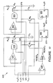
step 440 may be implemented in electronic hardware as set forth, for example, inFigures 6A and6B , which are schematic diagrams ofcircuits peak processing circuits edge detection systems circuits circuits circuits - The
circuit 600 operates as follows: The first derivative signal x'(t) is connected to the gate of a transistor M1. When x'(t) is positive and increasing, the transistor M1 turns on and conducts across its source and drain. The turn-on of the transistor M1 has two effects. First, the same currents flow across each of transistors M2 and M3, which form a current mirror. Second, that current charges a capacitor C1, as the transistor M1 and the capacitor C1 form a simple peak rectifier, and the voltage at thenode 610 is a peak-rectified version of x'(t). That charging continues until the voltage at thenode 610 equals that of x'(t) minus the gate-to-source voltage drop across the transistor M1 (VGSM1), and x'(t) stops increasing. During that time of charging, a mirror current flows through the transistor M3, thus pulling theoutput node 620 to a high voltage (approximately the positive supply voltage VDD). As long as x'(t) is increasing at a sufficient rate, the capacitor C1 will continue to charge, and the voltage of thenode 620 will remain high. - However, as x'(t) stops increasing, the voltage of the
node 620 will begin to discharge. The transistor M4 is set to have a drain-to-source current equal to IREF/3, while a transistor M5 is connected between thenode 620 and ground, which supplies a drain-to-source current equal to IREF. That is accomplished by use of a transistor M13, which forms a current mirror with the transistors M4 an M5. To achieve the unequal currents, the transistors M5 and M13 are preferably designed to have a channel width-to-length ratio three times that of the transistor M4, so that the drain-to-source current through each of the transistor M5 and M13 is three times that of transistor M4. Thus, the current through transistor M5, which discharges thenode 620, is IREF. The precise condition under which thenode 620 discharges is given by the following Equations (A) - (C):


- When the condition stated in Equation (C) is met, then the voltage at the
node 620 decays to ground at a rate determined by the parasitic capacitance at thenode 620 and the difference between the currents in M3 and M5, i.e., IREF - i(M3). When x'(t) stops charging the capacitor C1, such as after a local peak in x'(t), then no current flows through C1 and as a result i(M1) = IREF/3. Due to the current mirror, i(M3) = IREF/3 as well. Thus, in that case, the greater current IREF through the transistor M5 rather quickly pulls the voltage at thenode 620 low, where it stays until a larger subsequent value of x'(t) causes the capacitor C1 to charge further. - The initial decay rate of the voltage at the node 620 (after x"(t) < 2IREF/3C1 but before the capacitor C1 stops charging) should be carefully selected. If the initial decay rate is too fast, then the voltage at the
node 620 will decay to ground before x"(t) crosses zero, and no edges will be rendered. If the initial decay rate is too slow, then the gate will remain open and qualify trailing peaks which are near in time to the peak having maximum amplitude. For a given system, the reference current IREF is therefore ideally chosen to ensure that all legitimate edges are rendered while still rejecting as many trailing peaks as possible. - The transistor M4 provides a small DC current to overcome whatever leakage current may flow in the transistors M1 and M2. Without the current from M4, the leakage current from the transistors M1 and M2 would be integrated by the capacitor C1, causing the voltage at the
node 610 to increase to near VDD. Thus, the current in M4 should be chosen to be greater than the maximum possible leakage current through the transistors M1 and M2. If the current through M4 is too large, on the other hand, the gate-to-source voltage drop of M1 could become large enough to limit dynamic range, especially if the supply voltage VDD is low. Further, i(M4) must be significantly smaller than i(M5) to ensure that the voltage at thenode 620 drops quickly to ground after the first derivative slope drops below the threshold. By providing both currents from a common current mirror as shown, all of these conditions may be met. While a 3:1 ratio is used in this example, other ratios may be chosen which would also meet the above criteria. - In the absence of the first derivative signal x'(t), baseline noise can cause the voltage at the
node 620 to qualify illegitimate edges. To counteract that problem, which could cause a downstream decoder to expend resources processing spurious edges, potentially overloading the decoder to the point where legitimate edges are ignored, the voltage at thenode 620 is qualified by AND-ing it with the gated peak signal yR(t), which is true when x'(t) exceeds a threshold generated conventionally (as inU.S. Patent No. 4,000,397 ). The logical AND-ing of these two signals occurs at an ANDgate 625, as shown inFigure 6A . In this way the positive features of the conventional threshold gating (such as noise immunity in the absence of signal) and the added benefit of rejection of trailing peaks are both achieved. -
Figure 7 is a set of voltage-versus-time plots for various signals in thecircuit 600.Figure 7A is a plot of a portion of x'(t), just as inFigure 5 , and a plot of the voltage v610(t) across the capacitor C1 at thenode 610. While x'(t) is initially rising, the capacitor C1 is charging, and the voltage v610(t) tracks x'(t) except for a small voltage drop VGSM1 across the transistor M1. However, when x'(t) reaches a peak and begins falling, then the capacitor no longer charges and in fact begins discharging slowly due to the current in M4, until x'(t) exceeds the voltage v610(t) + VGSM1 again. Thus, the voltage v610(t) is a peak-rectified version of x'(t).Figure 7A also shows the threshold +T, which is applied to the generation of the signal yR(t).Figure 7B is a plot of x"(t), the derivative of x'(t). Also shown onFigure 7B is the threshold level 2IREF/3C1.Figure 7C is a plot of the voltage v620(t) at thenode 620. As explained above, the voltage v620(t) is at a high value when x"(t) exceeds the threshold level 21REF/3C1. Otherwise, the voltage V620 decays as shown.Figure 7D is a plot of yR(t), assuming the threshold shown inFigure 7A. Figure 7E is a plot of zR(t), which is the logical AND-ing of the voltage V620 and yR(t). As can be seen, zR(t) contains pulses corresponding to the peaks p1, p2, and p4, but not the trailing sub-maximum peaks p3, p5, and p6. - With reference to
Figure 6B , thecircuit 605 comprises acomparator 630, an optional ANDgate 635, a resistor Rs, a transistor MS, and a capacitor CS, which together form apeak detector 638. Thepeak detector 638 detects peaks in the first derivative signal x'(t) as follows: Ignoring for the moment the AND gate 635 (or assuming for the moment that u(t) is high, meaning that x'(t) is rising), then thenode 640, which is connected to the gate of the transistor MS, is high and therefore turns on the transistor MS whenever the first derivative signal x'(t) exceeds the voltage across the capacitor CS at thenode 645. In that case, the first derivative signal x'(t) is connected to thenode 645 across the resistor Rs, causing the voltage at thenode 645 to track the first derivative signal x'(t). When the first derivative signal x'(t) begins to decrease, the accumulated charge on the capacitor Cs causes the voltage at thenode 645 to be greater than the first derivative signal x'(t), causing thecomparator 630 output to go low, which causes the voltage at thenode 640 to go low, which in turn causes the transistor MS to turn off. In that case, the capacitor CS holds its accumulated charge and the voltage of thenode 645 remains essentially constant unless and until the first derivative signal x'(t) exceeds the voltage at thenode 645. In other words, thepeak detector 638 tracks the first derivative signal x'(t) while it is increasing beyond a previous peak, or holds at a peak value until that peak value is again exceeded. Thus, for example, with reference toFigure 5 , thepeak detector 638 would track to and thereafter hold at the maximum peak p4, as shown in simplistic form inFigure 8A . - While the transistor MS is illustrated as a field-effect transistor (FET), it may be of any type of switching transistor or other suitable switch. The transistor MS functions as a switch, where the gate terminal is a control terminal controlling whether there is conduction between controllable conduction terminals, viz., the drain and source terminals.
- The
peak detector 638 differs from a conventional peak detector; which typically would connect the drain terminal of the transistor MS to a positive supply voltage. An advantage of the peak detector in thecircuit 605 is that it exhibits significantly less overshoot than the conventional implementation. That advantage can be important when processing high bandwidth signals, as often occurs in bar code reading. Overshoot occurs when thecomparator 630 has a non-zero propagation delay that delays turn off of the transistor MS. If, as in the conventional peak detector, the drain terminal of the transistor MS were connected to a positive supply voltage, then significant additional charge could accumulate on the capacitor Cs during that slight delay time. Because the drain terminal of the transistor MS is connected to the input signal, rather than a supply voltage, there is no additional charging of the capacitor CS during the comparator's turn-off delay. Instead, there may be some undershoot resulting from discharging of the capacitor Cs as the input signal begins to decrease during the comparator's turn-off delay. Fortunately, that undershoot is considerably smaller in magnitude than the overshoot that the conventional implementation exhibits, as the input signal typically has a fairly flat slope near the time of turn-off. - The parameters of the capacitor CS, the resistor RS, and the transistor MS are preferably chosen to satisfy application-specific constraints, such as input signal bandwidth, available circuitry area, and tolerable charge injection. For example, the time constant resulting from the product of Cs and Rs should be sufficiently small to permit the circuit to respond to variations in the input signal. Furthermore, charge injection becomes more problematic as the size of the capacitor CS decreases, and as the size of transistor MS increases. If the capacitance gets too large, it can affect the stability of the amplifier providing the input signal; resistor RS should therefore be large enough to isolate the amplifier output from this capacitance while in the tracking mode. Those and other considerations can be taken into account in determining suitable parameter values characterizing the capacitor CS, the resistor RS, and the transistor MS.
- The AND
gate 635 is an optional component in thecircuit 605. If included, as shown inFigure 6B , it can hasten the turn-off of the transistor MS, as the second derivative polarity signal u(t) tends to become negative earlier than thecomparator 630 recognizes that a peak has been reached. One reason that thecomparator 630 has a non-zero response time during transitions of its inputs is that thecomparator 630 has a finite gain and has limited overdrive when its inputs are nearly equal, as is the case during transitions from tracking to holding modes at or near the peaks of the input signal. - Not shown in
Figure 6B is reset circuitry to short the capacitor CS at the conclusion of a half-cycle. Such reset circuitry is illustrated inFigure 10 , which is discussed below. -
Figure 8B illustrates a more realistic plot of the behavior of the peak detector portion of thecircuit 605 than the simplified one inFigure 8A . TheFigure 8B plot was generated by computer simulation of thecircuit 605 for a case in which the signal strength is quite small (in fact, near the lower limit to acceptably read bar codes). As can be seen, the voltage at thenode 645 is generally slightly less than the first derivative signal x'(t). That tracking error becomes less significant as the signal strength increases and in fact is negligible at typical signal strength.Figure 7B also illustrates some pedestal error in the voltage at thenode 645. That appears as "shelves" 710 in the v645(t) waveform after each positive peak in the first derivative signal x'(t), where v645(t) in hold mode is slightly less than the voltage of the preceding peak. The pedestal error is due, in part, to overshoot attributable to finite response time by thecomparator 630. The pedestal error is also due, in part, to charge injection in the transistor MS. - Besides the peak detector explained above, the
circuit 605 also comprises a set-reset flip-flop 650. Thenode 640 is connected to the set input of the flip-flop 650, while the STV signal is connected to the reset input of the flip-flop 650. The operation of the flip-flop 650 can be understood by considering the signals depicted inFigure 8B . As the first derivative signal x'(t) is increasing, thepeak detector 638 is in its tracking mode and the voltage atnode 640 is high. This state is shown initially inFigure 8B from about 30 µs to about 31 µs. During this time, the high value at thenode 640 sets the flip-flop 650, causing the signal wS(t) output from the flip-flop 650 to be high. After a slight propagation delay following the first positive peak shown inFigure 8B , the signals wS(t), yS(t) and u(t) are all high, causing the STV signal to be asserted. The STV signal then resets the flip-flop 650. As x'(t) begins to decrease after the first peak, the peak detector enters its holding mode, and the voltage at thenode 640 is low, in which case the flip-flop 650 remains reset and wS(t) remains low. That condition continues until x'(t) increases again and surpasses its previous peak (occurring somewhat after about 32 µs inFigure 8B ), at which point thepeak detector 638 switches to its tracking mode, causing the flip-flop 650 to set. At the next peak of x'(t) the STV signal is again asserted briefly until the flip-flop 650 is reset. This process repeats every time x'(t) rises to a peak of greater magnitude than any previous peak during a half-cycle. As a result, in the example depicted inFigure 7B , for instance, the STV signal is asserted near the peaks p1, p2, and p4, but not the peaks p3, p5, and p6. Among the qualified peaks p1, p2, and p4, subsequent processing detects the last one p4, which is the maximum and best choice among the multiple peaks in the half cycle. -
Figure 9 and10 are schematic diagrams ofillustrative circuits peak processing circuit circuits - The
circuit 800 contains two separate circuits, each like thecircuit 600, one for each signal of the differential pair. The first circuit, which processes x'P(t) comprises the transistors M1 - M5, capacitor C1, and thenodes circuit 600. The other circuit, which processes x'N(t), comprises transistors M7 - M11, a capacitor C2, andnodes nodes - In addition, the
circuit 800 comprises additional circuitry to selectively enable and disable the two circuits such that only one operates at any given time. That additional circuitry comprises acomparator 810, aninverter 820, and two transistors M6 and M12. The inputs of thecomparator 810 are the differential pair x'P(t) and x'N(t). The output of thecomparator 810 is a signal labeled RESETN, which is input to theinverter 820 to produce a signal labeled RESETP. The signal RESETN is high and the signal RESETP is low during a positive half cycle of x'(t), when x'P(t) > x'N(t). During that time, the signal RESETN, which is connected to the gate of the transistor M12, causes the transistor M12 to turn on and thereby to short the capacitor C2. Also, during that time, the signal RESETP, which is connected to the gate of the transistor M6, causes the transistor M6 to turn off, thus allowing the capacitor C1 to charge in response to x'P(t) and the first circuit to operate normally. Conversely, during a negative half cycle of x'(t), when x'N(t) > x'P(t), the transistor M6 turns on, shorting the capacitor C1, while the transistor M12 turns off, allowing the second circuit to operate normally. - Finally, the
circuit 800 comprises two similar circuits for combining the voltages at thenodes inverter 830 with hysteresis, a negative-input ANDgate 840, and aninverter 850. The second of those circuits comprises aninverter 860 with hysteresis, a negative-input ANDgate 870, and aninverter 880 in an identical configuration. The particular configuration of those elements in thecircuit 800 is for the case when yS(t), yR(t), zS(t), and zR(t) are low-true signals. - With reference to
Figure 10 , thecircuit 805 contains two separate circuits, each like thecircuit 605, one for each signal of the differential pair. The first circuit, which processes x'P(t), comprises thecomparator 630, ANDgate 635, transistor MS, capacitor CS, resistor Rs, set-reset flip-flop 650 and thenodes circuit 605. The other circuit, which processes x'N(t), comprises corresponding elements:comparator 660, ANDgate 665, transistor MR, capacitor CR, resistor RR, set-reset flip-flop 680, andnodes - In addition, the
circuit 805 comprises circuitry to selectively enable and disable the two complementary circuits such that only one operates at any given time. That additional circuitry comprises acomparator 690, aninverter 695, and two transistors MP and MN. The inputs of thecomparator 690 are the differential pair. The output of thecomparator 690 is a signal labeled RESETN, which is input to theinverter 695 to produce a signal labeled RESETP. The signal RESETN is high and the signal RESETP is low during a positive half cycle of x'(t), when x'P(t) > x'N(t). During that time, the signal RESETN, which is connected to the gate of the transistor MN, causes the transistor MN to turn on and thereby to discharge the capacitor CR to a DC reference voltage VREF, which is the reference voltage for the differential pair x'P(t) and x'N(t), where x'P(t) - VREF = VREF - x'N(t). Also, during that time, the signal RESETP, which is connected to the gate of the transistor MP, causes the transistor MP to turn off, thus allowing the capacitor Cs to charge in response to x'P(t) and the first circuit to operate normally. Conversely, during a negative half cycle of x'(t), when x'N(t) > x'P(t), the transistor MP turns on, discharging the capacitor CS, while the transistor MN turns off, allowing the second circuit to operate normally. The reference voltage VREF can be seen inFigure 8B at a level slightly below 1.54 volts. - The
circuits circuits circuits - Moreover, the
circuits method 400. Although the analog form of thecircuit 805 is preferred at the present time because of its lower cost and power consumption, those factors may change in the future. - More generally, the
method 400 and optional improvements tomethod 400 can be implemented in special-purpose digital hardware or programmed for execution on a processor. For example,improvement methods Figures 11A and 11B , respectively. - The
method 900A begins by generating (step 910) a scan line signal x(t) and differentiating (step 920) it twice to yield x'(t) and x"(t). Next, the method 900 detects (step 930) zero crossings of x"(t). It is the zero crossings of x"(t) that indicate, albeit possibly ambiguously, locations of edges in the binary optical code that the scan line signal x(t) represents, albeit imperfectly. To resolve that possible ambiguity, themethod 900A performs aqualifying step 940 and a choosingstep 950. Thequalifying step 940 detects the substantially simultaneous occurrence of two conditions: (1) x"(t) having a magnitude greater than a threshold, i.e., |x"(t)| > T2, and (2) x'(t) having a maximum magnitude since its last zero crossing. Thecircuit 600 performs thequalifying step 940 in analog form, where the threshold T2 = 2IREF/3C1, and the voltage v610(t) at thenode 610 approximately tracks the maximum magnitude of x'(t) over a half cycle. Referring toFigure 7C , the voltage v620(t) at thenode 620 represents substantially simultaneous occurrence of conditions (1) and (2) for a positive half cycle. Finally, themethod 900A chooses (step 950) the most likely one of the qualified zero crossings of x"(t). As explained above, that is the one occurring last in time in a half cycle of x'(t). - The
method 900B begins by is similar to themethod 900A, except that themethod 900B alternately tracks and holds (step 932) x'(t) with a peak detector, such as thepeak detector 638, as x'(t) varies over time. Tracking preferably involves tracking the x'(t) signal while it is not less than a previous one of the multiple like-polarity successive local peaks in a half cycle, while holding preferably involves holding a value approximately equal to a peak that is greater than any previous one of the multiple like-polarity successive local peaks in the first derivative, until a larger magnitude peak in the series of multiple like-polarity successive local peaks is encountered. Indeed, steps are preferably taken to insure that the stored value is as close as possible to the voltage of the associated peak. For example, thecircuit 605 connects the drain terminal of the transistor MS to x'(t) rather than a positive supply to accomplish that goal. Moreover, themethod 900B preferably expedites the transitions from tracking to holding to improve response time, which in turn reduces the error of the stored value. For example, thecircuit 605 utilizes u(t) via the ANDgate 635 to accomplish that goal. - Note that the steps of the
methods Figures 11A and 11B are presented in a simplified, linear order of steps to most readily teach the concepts involved, not to imply a particular order of operations. - The methods and systems illustrated and described herein can exist in a variety of forms both active and inactive. For example, they can exist as one or more software programs comprised of program instructions in source code, object code, executable code or other formats. Any of the above can be embodied on a computer-readable medium, which include storage devices and signals, in compressed or uncompressed form. Exemplary computer-readable storage devices include conventional computer system RAM (random access memory), ROM (read only memory), EPROM (erasable, programmable ROM), EEPROM (electrically erasable, programmable ROM), flash memory and magnetic or optical disks or tapes. Exemplary computer-readable signals, whether modulated using a carrier or not, are signals that a computer system hosting or running a computer program can be configured to access, including signals downloaded through the internet or other networks. Concrete examples of the foregoing include distribution of software on a CD ROM or via Internet download. In a sense, the Internet itself, as an abstract entity, is a computer-readable medium. The same is true of computer networks in general.
Claims (17)
- A method (400) for detecting edges in a binary optical code by processing a signal (x(t)) imperfectly indicating perceived regions of relatively dark and relatively light areas arranged in an alternating pattern as part of a binary optical code, and by differentiating (420) the signal (x(t)) to form a first derivative (x'(t)) of the signal, the first derivative (x'(t)) having at least in part a series of successive local peaks of the same polarity, the method characterized in that it includes the steps of:ignoring (440) peaks in the series having a peak value less than any previous peak value in the series, thereby producing a resulting set of unignored peaks;choosing (450) from the unignored peaks in the series the one peak occurring last in order; andgenerating, according to the chosen peak, a signal (STV, RTV) indicative of an edge between a light area and a dark area in the pattern.
- The method (400) of claim 1, wherein the ignoring step (440) comprises:peak-rectifying the first derivative signal; andselectively charging or discharging a node based on the peak-rectifying step.
- The method (400) of claim 2, wherein the peak-rectifying step generates a peak rectified version of the first derivative, and the step of selectively charging or discharging comprises:charging the node while the first derivative is rising by at least a predetermined rate; anddischarging the node while the first derivative is not rising.
- The method (400) of claim 1, further comprising: comparing the first derivative to a threshold, and wherein the generating step is further based in-part on the comparison of the first derivative to the threshold.
- The method (400) of claim 1, further comprising:differentiating the first derivative so as to form (920) a second derivative ((x"(t)) of the signal, wherein the second derivative may have multiple zero crossings for a given edge in the binary optical code;detecting (930) the zero crossings of the second derivative;qualifying (940) a zero crossing of the second derivative by identifying among the multiple zero crossings of the second derivative the first one occurring after the substantially simultaneous occurrence of the second derivative exceeding a threshold and the first derivative having a magnitude greater than at any previous time since a last zero crossing of the first derivative; andwherein the generating step (STV, RTV) is further based in-part on a set of one or more qualified zero crossings of the second derivative indicating possible positions for the given edge in the binary optical code.
- The method (400, 900A) of claim 5, further comprising:choosing (950), as a unique indication of the position of the given edge, the qualified zero crossing of the second derivative that occurs last in time in the set of one or more qualified zero crossings of the second derivative.
- The method (400) of claim 1, wherein the optical code is a bar code, the relatively light areas are spaces in the bar code, and the relatively dark areas are bars in the bar code.
- The method (400) of claim 1, wherein the series of local peaks of the same polarity is a series of positive local peaks.
- The method (400) of claim 1, wherein the differentiating, ignoring, choosing, and generating steps are performed by one or more of the group consisting of a processor and a digital logic circuit.
- The method (400) of claim 1, wherein the ignoring step (440) comprises:tracking (932) the first derivative while it is not less than a previous one of the successive local peaks of the same polarity in the first derivative;holding (932) a value approximately equal to a peak that is greater than any previous one of the multiple like-polarity successive local peaks in the first derivative, until a larger magnitude peak in the series of multiple like-polarity successive local peaks is encountered; andswitching between the tracking step and the holding step as the first derivative varies over time.
- A circuit (300, 305) for detecting edges in a binary optical code, the circuit having a means for receiving a signal (x(t)) imperfectly indicating perceived regions of relatively dark and relatively light areas arranged in an alternating pattern as part of a binary optical code, and the circuit having a means (220) for differentiating the signal (x(t)) to form a first derivative (x'(t)) of the signal, wherein the first derivative (x'(t)) may have a series of successive local peaks of the same polarity, the circuit characterized in that it includes:means (310, 320) for ignoring peaks in the series having a peak value less than any previous peak value in the series, thereby resulting in a set of unignored peaks;means (310, 320) for choosing from the unignored peaks in the series the one peak occurring last in order; andmeans for generating, according to the chosen peak, a signal (STV, RTV) indicative of an edge between a light area and a dark area in the pattern.
- The circuit (300, 305) of claim 11, wherein the means (310, 320) for ignoring comprises:means for peak-rectifying the first derivative signal so as to generate a peak rectified version of the first derivative; andmeans for selectively charging or discharging a node based on the peak rectified version of the first derivative.
- The circuit (300, 305) of claim 12, wherein the means for selectively charging or discharging comprises:means for charging the node while the first derivative is rising by at least a predetermined rate; andmeans for discharging the node while the first derivative is not rising.
- The circuit (300, 305) of claim 11, wherein the means (310, 320) for ignoring comprises:means for tracking the first derivative while it is not less than a previous one of the successive local peaks of the same polarity in the first derivative;means for holding a value approximately equal to a peak that is greater than any previous one of the multiple like-polarity successive local peaks in the first derivative, until a larger magnitude peak in the series of multiple like-polarity successive local peaks is encountered; andmeans for switching between the tracking step and the holding step as the first derivative varies over time.
- The circuit (305) of claim 11, wherein the means (310, 320) for ignoring comprises:a peak detector (638) having an input receiving the input signal (x'(t)), the peak detector (638) approximately tracking the input signal (x'(t)) while the absolute value of the input signal (x'(t)) is both (a) increasing and (b) greater than at any previous time during the half-cycle, the peak detector otherwise approximately holding during the half-cycle near those local peaks having increasingly larger magnitudes in the series of multiple successive peaks of the same polarity as the half-cycle;a node (640) in the peak detector (638) having a voltage indicative of whether the peak detector (638) is in a tracking state or a holding state; anda set-reset flip-flop (650) having a set input connected to the node (640), whereby the output of the flip-flop (650) is set when the peak detector (638) is in a tracking state.
- A circuit (605) according to claim 15, wherein the peak detector (638) comprises a comparator (630) having two inputs and an output, a switch having a control terminal and two controllable conduction terminals, a capacitor (CS), and a resistor (RS); wherein the input signal (x'(t)) is connected to a first of the comparator (630) inputs, the comparator (630) output is connected to the switch control terminal, the resistor (RS) is connected between one of the conduction terminals of the switch and the input signal (x'(t)), the capacitor (CS) is connected to the other of the conduction terminals of the switch, and the voltage across the capacitor (CS) is input to the second of the comparator (630) inputs.
- The circuit (605) according to claim 15, wherein the flip-flop (650) has a reset input receiving a signal indicating detection of an edge of a feature in a binary optical code.
Applications Claiming Priority (3)
| Application Number | Priority Date | Filing Date | Title |
|---|---|---|---|
| US10/866,308 US7201322B2 (en) | 2004-06-10 | 2004-06-10 | System, circuit, and method for edge detection in a binary optical code |
| US11/039,193 US7204422B2 (en) | 2004-06-10 | 2005-01-18 | System, circuit, and method for edge detection in a binary optical code |
| PCT/US2005/020346 WO2005124661A1 (en) | 2004-06-10 | 2005-06-08 | System, circuit, and method for edge detection in a binary optical code |
Publications (4)
| Publication Number | Publication Date |
|---|---|
| EP1771810A1 EP1771810A1 (en) | 2007-04-11 |
| EP1771810A4 EP1771810A4 (en) | 2010-12-01 |
| EP1771810B1 true EP1771810B1 (en) | 2014-03-12 |
| EP1771810B8 EP1771810B8 (en) | 2014-06-11 |
Family
ID=35509921
Family Applications (1)
| Application Number | Title | Priority Date | Filing Date |
|---|---|---|---|
| EP05765457.6A Expired - Lifetime EP1771810B8 (en) | 2004-06-10 | 2005-06-08 | System, circuit, and method for edge detection in a binary optical code |
Country Status (3)
| Country | Link |
|---|---|
| US (1) | US7204422B2 (en) |
| EP (1) | EP1771810B8 (en) |
| WO (1) | WO2005124661A1 (en) |
Families Citing this family (10)
| Publication number | Priority date | Publication date | Assignee | Title |
|---|---|---|---|---|
| US7093763B1 (en) * | 2005-02-25 | 2006-08-22 | Symbol Technologies, Inc. | Laser scanner having analog digitizer with increased noise immunity |
| JP2008282262A (en) * | 2007-05-11 | 2008-11-20 | Olympus Corp | Bar code reader and bar code reading method |
| US8172145B2 (en) * | 2007-11-20 | 2012-05-08 | Datalogic ADC, Inc. | Enhanced virtual scan line processing |
| US8459556B2 (en) * | 2009-01-09 | 2013-06-11 | Datalogic ADC, Inc. | Prioritized virtual scan line processing |
| JP5398653B2 (en) * | 2010-06-30 | 2014-01-29 | 株式会社オプトエレクトロニクス | Decoding method and decoding processing apparatus |
| US9141841B2 (en) | 2012-12-20 | 2015-09-22 | Ebay, Inc. | Methods, system and apparatus for conducting a point of sale transaction |
| AT515932B1 (en) * | 2014-10-27 | 2016-01-15 | Bernecker & Rainer Ind Elektronik Gmbh | Method and device for detecting a printed mark |
| DE102016100261A1 (en) * | 2016-01-08 | 2017-07-13 | Nanofocus Ag | Method for electronic analysis of a time-varying signal |
| US10381036B1 (en) * | 2016-02-16 | 2019-08-13 | Seagate Technology Llc | Laser bias calibration |
| WO2025230513A1 (en) * | 2024-04-30 | 2025-11-06 | Siemens Medical Solutions Usa, Inc. | Methods and apparatus for medical imaging event timing determination and image reconstruction |
Family Cites Families (15)
| Publication number | Priority date | Publication date | Assignee | Title |
|---|---|---|---|---|
| US4000397A (en) * | 1975-03-21 | 1976-12-28 | Spectra-Physics, Inc. | Signal processor method and apparatus |
| US5734152A (en) * | 1995-05-31 | 1998-03-31 | Symbol Technologies, Inc. | Optical scanners and signal processors therefor |
| US5302813A (en) * | 1992-04-02 | 1994-04-12 | Symbol Technologies, Inc. | Multi-bit digitizer |
| US5449893A (en) * | 1992-04-02 | 1995-09-12 | Symbol Technologies, Inc. | Digitizer for bar code reader |
| US6164540A (en) * | 1996-05-22 | 2000-12-26 | Symbol Technologies, Inc. | Optical scanners |
| US5514858A (en) * | 1995-02-10 | 1996-05-07 | Intermec Corporation | Method and apparatus for decoding unresolved complex multi-width bar code symbology profiles |
| DE69634584T2 (en) * | 1995-05-31 | 2005-09-15 | Symbol Technologies, Inc. | Optical scanner |
| US5633488A (en) * | 1995-12-19 | 1997-05-27 | Webscan, Inc. | Method and apparatus to enable the high speed evaluation of bar code indicia |
| US6012639A (en) * | 1996-11-01 | 2000-01-11 | Psc Scanning Inc. | Edge detection method and apparatus for shot noise limited signals |
| US6073849A (en) | 1996-11-01 | 2000-06-13 | Psc Scanning, Inc. | Electronic edge detection system using a second derivative signal processor |
| US6012640A (en) * | 1997-07-08 | 2000-01-11 | Intermec Ip Corporation | Rule based and fuzzy logic method and apparatus for processing reflectance signals from machine-readable symbols or images |
| WO2000016240A1 (en) * | 1998-09-14 | 2000-03-23 | Psc Scanning, Inc. | Fast edge detection system tolerant of high degree of intersymbol interference |
| US6918540B2 (en) * | 2000-04-18 | 2005-07-19 | Metrologic Instruments, Inc. | Bioptical point-of-sale (pos) scanning system employing dual polygon-based laser scanning platforms disposed beneath horizontal and vertical scanning windows for 360° omni-directional bar code scanning |
| EP1752909A1 (en) * | 2001-01-26 | 2007-02-14 | Fujitsu Ltd. | Information reading method and device, signal capturing method for information reading device, band limiting method therefor, timing point amplitude extracting method therefor, and signal processing method therefor |
| SE0301143D0 (en) * | 2003-04-17 | 2003-04-17 | C Technologies Ab | Method and device for loading data |
-
2005
- 2005-01-18 US US11/039,193 patent/US7204422B2/en not_active Expired - Lifetime
- 2005-06-08 WO PCT/US2005/020346 patent/WO2005124661A1/en not_active Ceased
- 2005-06-08 EP EP05765457.6A patent/EP1771810B8/en not_active Expired - Lifetime
Also Published As
| Publication number | Publication date |
|---|---|
| EP1771810A1 (en) | 2007-04-11 |
| US20050274809A1 (en) | 2005-12-15 |
| EP1771810A4 (en) | 2010-12-01 |
| US7204422B2 (en) | 2007-04-17 |
| WO2005124661A1 (en) | 2005-12-29 |
| EP1771810B8 (en) | 2014-06-11 |
Similar Documents
| Publication | Publication Date | Title |
|---|---|---|
| EP0193762B1 (en) | Low powered high ambient light bar code reader circuit | |
| US6499662B1 (en) | Fast edge detection system tolerant of high degree of intersymbol interference | |
| US7201322B2 (en) | System, circuit, and method for edge detection in a binary optical code | |
| US7204422B2 (en) | System, circuit, and method for edge detection in a binary optical code | |
| WO1999023598A1 (en) | Electronic edge detection system | |
| EP1443450B1 (en) | Optical barcode scanner | |
| US6508404B2 (en) | Symbology scanning system for efficiently locating coded symbologies | |
| US6012639A (en) | Edge detection method and apparatus for shot noise limited signals | |
| US9367716B2 (en) | Information reproduction device and information reproduction method | |
| US5608201A (en) | Method and apparatus for detecting edges in a signal obtained from a bar code scanned in the Fresnel zone | |
| US5864129A (en) | Bar code digitizer including a voltage comparator | |
| JP2716298B2 (en) | Barcode signal binarization device | |
| JPH06348877A (en) | Binarization circuit and CCD solid-state imaging device | |
| US20060065734A1 (en) | Dual scanner signal acquisition | |
| JP2923375B2 (en) | Barcode reader | |
| JP5391102B2 (en) | Ternary barcode detection method and detection apparatus | |
| JP2001028045A (en) | Binarization circuit and code reader | |
| JP2745945B2 (en) | Barcode detection device | |
| JP2732911B2 (en) | Article detection method | |
| JPH0751635Y2 (en) | Binary signal reader | |
| JPS58120111A (en) | Binary coding device for analog image signal | |
| JP3453896B2 (en) | Binarization circuit, solid-state imaging device having the same, and bar code reader using the same | |
| JPH11191220A (en) | Optical disk apparatus and optical disk reproducing method | |
| JP2852172B2 (en) | Write detection circuit | |
| JPH02184108A (en) | Binarizing device |
Legal Events
| Date | Code | Title | Description |
|---|---|---|---|
| PUAI | Public reference made under article 153(3) epc to a published international application that has entered the european phase |
Free format text: ORIGINAL CODE: 0009012 |
|
| 17P | Request for examination filed |
Effective date: 20070102 |
|
| AK | Designated contracting states |
Kind code of ref document: A1 Designated state(s): DE FR GB |
|
| RAP1 | Party data changed (applicant data changed or rights of an application transferred) |
Owner name: DATALOGIC SCANNING, INC. |
|
| DAX | Request for extension of the european patent (deleted) | ||
| RBV | Designated contracting states (corrected) |
Designated state(s): DE FR GB |
|
| A4 | Supplementary search report drawn up and despatched |
Effective date: 20101028 |
|
| 17Q | First examination report despatched |
Effective date: 20110630 |
|
| GRAP | Despatch of communication of intention to grant a patent |
Free format text: ORIGINAL CODE: EPIDOSNIGR1 |
|
| INTG | Intention to grant announced |
Effective date: 20131010 |
|
| GRAS | Grant fee paid |
Free format text: ORIGINAL CODE: EPIDOSNIGR3 |
|
| GRAA | (expected) grant |
Free format text: ORIGINAL CODE: 0009210 |
|
| AK | Designated contracting states |
Kind code of ref document: B1 Designated state(s): DE FR GB |
|
| REG | Reference to a national code |
Ref country code: GB Ref legal event code: FG4D |
|
| RAP2 | Party data changed (patent owner data changed or rights of a patent transferred) |
Owner name: DATALOGIC ADC, INC. |
|
| REG | Reference to a national code |
Ref country code: DE Ref legal event code: R096 Ref document number: 602005042940 Country of ref document: DE Effective date: 20140417 |
|
| REG | Reference to a national code |
Ref country code: DE Ref legal event code: R097 Ref document number: 602005042940 Country of ref document: DE |
|
| PLBE | No opposition filed within time limit |
Free format text: ORIGINAL CODE: 0009261 |
|
| STAA | Information on the status of an ep patent application or granted ep patent |
Free format text: STATUS: NO OPPOSITION FILED WITHIN TIME LIMIT |
|
| 26N | No opposition filed |
Effective date: 20141215 |
|
| GBPC | Gb: european patent ceased through non-payment of renewal fee |
Effective date: 20140612 |
|
| REG | Reference to a national code |
Ref country code: DE Ref legal event code: R097 Ref document number: 602005042940 Country of ref document: DE Effective date: 20141215 |
|
| PG25 | Lapsed in a contracting state [announced via postgrant information from national office to epo] |
Ref country code: GB Free format text: LAPSE BECAUSE OF NON-PAYMENT OF DUE FEES Effective date: 20140612 |
|
| REG | Reference to a national code |
Ref country code: FR Ref legal event code: PLFP Year of fee payment: 12 |
|
| REG | Reference to a national code |
Ref country code: FR Ref legal event code: PLFP Year of fee payment: 13 |
|
| REG | Reference to a national code |
Ref country code: FR Ref legal event code: PLFP Year of fee payment: 14 |
|
| PGFP | Annual fee paid to national office [announced via postgrant information from national office to epo] |
Ref country code: FR Payment date: 20180620 Year of fee payment: 14 |
|
| PG25 | Lapsed in a contracting state [announced via postgrant information from national office to epo] |
Ref country code: FR Free format text: LAPSE BECAUSE OF NON-PAYMENT OF DUE FEES Effective date: 20190630 |
|
| REG | Reference to a national code |
Ref country code: DE Ref legal event code: R079 Ref document number: 602005042940 Country of ref document: DE Free format text: PREVIOUS MAIN CLASS: G06K0009180000 Ipc: G06V0030224000 |
|
| P01 | Opt-out of the competence of the unified patent court (upc) registered |
Effective date: 20230530 |
|
| PGFP | Annual fee paid to national office [announced via postgrant information from national office to epo] |
Ref country code: DE Payment date: 20240619 Year of fee payment: 20 |
|
| REG | Reference to a national code |
Ref country code: DE Ref legal event code: R071 Ref document number: 602005042940 Country of ref document: DE |