EP1770865A1 - Area efficient fracturable logic elements - Google Patents
Area efficient fracturable logic elements Download PDFInfo
- Publication number
- EP1770865A1 EP1770865A1 EP06019794A EP06019794A EP1770865A1 EP 1770865 A1 EP1770865 A1 EP 1770865A1 EP 06019794 A EP06019794 A EP 06019794A EP 06019794 A EP06019794 A EP 06019794A EP 1770865 A1 EP1770865 A1 EP 1770865A1
- Authority
- EP
- European Patent Office
- Prior art keywords
- inputs
- multiplexer
- luts
- output
- multiplexers
- Prior art date
- Legal status (The legal status is an assumption and is not a legal conclusion. Google has not performed a legal analysis and makes no representation as to the accuracy of the status listed.)
- Granted
Links
Images



Classifications
-
- H—ELECTRICITY
- H03—ELECTRONIC CIRCUITRY
- H03K—PULSE TECHNIQUE
- H03K19/00—Logic circuits, i.e. having at least two inputs acting on one output; Inverting circuits
- H03K19/02—Logic circuits, i.e. having at least two inputs acting on one output; Inverting circuits using specified components
- H03K19/173—Logic circuits, i.e. having at least two inputs acting on one output; Inverting circuits using specified components using elementary logic circuits as components
- H03K19/1733—Controllable logic circuits
- H03K19/1737—Controllable logic circuits using multiplexers
Definitions
- the present application relates to logic elements for use with programmable logic devices or other similar devices.
- PLDs Programmable logic devices
- CPLDs CPLDs
- PALs PLAs
- PLAs PLAs
- FPLAs FPLAs
- EPLDs EEPLDs
- LCAs LCAs
- FPGAs FPGAs
- PLDs Programmable logic devices
- Such devices are well known in the art and typically provide an "off the shelf” device having at least a portion that can be electrically programmed to meet a user's specific needs.
- ASICs Application specific integrated circuits
- ASICs have traditionally been fixed integrated circuits, however, it is possible to provide an ASIC that has a portion or portions that are programmable; thus, it is possible for an integrated circuit device to have qualities of both an ASIC and a PLD.
- PLD as used herein will be considered broad enough to include such devices.
- PLDs typically include blocks of logic elements, which are sometimes referred to as logic array blocks (“LABs”) or “configurable logic blocks” (“CLBs”).
- Logic elements which are also referred to by other names such as “logic circuits” or “logic cells”, may include a look-up table (“LUT”), product term, carryout chain, register, and other elements.
- Logic elements typically include configurable elements holding configuration data that determine the particular function or functions carried out by the logic element.
- a typical LUT circuit may include RAM bits that hold data (a "1" or “0").
- Other types of configurable elements may be used. Some examples may include static, magnetic, ferro-electric or dynamic random access memory, electrically erasable read-only memory, flash, fuse, and anti-fuse programmable connections.
- the programming of configuration elements could also be implemented through mask programming during fabrication of the device. While mask programming may have disadvantages relative to some of the field programmable options already listed, it may be useful in certain high volume applications.
- the generic term "memory element" will be used to refer to any programmable element that may be configured to determine functions implemented by a PLD.
- K-LUT K-input lookup table
- K-LUT typically includes 2 K programmable memory elements, and a 2K to 1 multiplexer tree, selecting one of the storage elements under the control of the K select inputs to the multiplexer.
- K inputs can be considered to be the inputs to a K-input logic function which can implement any particular required logic function by setting the contents of the memory elements to the appropriate values.
- the 6-LUT circuitry are offset by a reduction in the delay.
- the longest path through a logic circuit might be ten 4-LUTs versus eight 6-LUTs.
- the 6-LUT version of the circuit might be larger, but faster.
- the 6-LUT circuit would likely require less programmable routing in a PLD, offsetting some of its higher cost.
- the eight-hundred 6-LUTs might actually include three-hundred 6-input functions, three-hundred 5-input functions, one-hundred 4-input functions, and one-hundred 3-input functions.
- the LE based on 6-LUTs is only being used to its fullest extent in three-hundred out of eight-hundred instances.
- a fracturable logic element includes a first, second, third, and fourth two-input lookup tables (2-LUTs). Each 2-LUT includes four memory elements. Each memory element is configured to hold one data bit.
- the fracturable logic element also includes a set of six inputs and a control circuit configured to operate in a first mode and a second mode. When the control circuit operates in the first mode, a first combinatorial output is generated using four of the set of six inputs and the first, second, third, and fourth 2-LUTs. When the control circuit operates in the second mode, a second combinatorial output is generated using a first subset of three of the set of six inputs and the first and second 2-LUTS.
- a third combinatorial output is generated using a second subset of three of the set of six inputs and the third and fourth 2-LUTs, the first and second subsets being non-intersecting subsets of the set of six inputs.
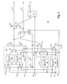
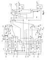
- Fig. 1 is a schematic of an exemplary two-input lookup table (2-LUT);
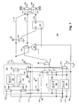
- Fig. 2 is a schematic of an exemplary fracturable logic element
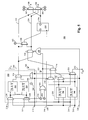
- Fig. 3 is a schematic of another exemplary fracturable logic element
- Fig. 4 is a schematic of another exemplary fracturable logic element
- Fig. 5 is a schematic of another exemplary fracturable logic element
- Fig. 6 is a schematic of another exemplary fracturable logic element
- Fig. 7 is a schematic of another exemplary fracturable logic element
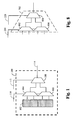
- Fig. 8 is a schematic of an exemplary 4:1 multiplexer implemented as a tree of 2:1 multiplexers
- Fig. 9 is a schematic of another exemplary fracturable logic element.
- Fig. 10 is a block diagram of an exemplary data processing system.
- 2-LUT 100 includes memory elements 102 connected to 2:1 multiplexers 104, 106.
- each memory element 102 can hold one data bit (i.e., 1 or 0), and each is coupled to provide that bit to an input of multiplexers 104, 106.
- the control inputs of multiplexers 104, 106 are connected to input 110.
- the outputs of multiplexers 104, 106 are connected to 2:1 multiplexer 108.
- the control input of multiplexer 108 is connected to input 112.
- inputs 110, 112 can be used to selected any one of memory element 102 as an output 114 of 2-LUT 100.
- Logic element 200 includes four 2-LUTs 202, 204, 206, and 208 and a set of six inputs 210, 212, 214, 216, 218, and 220.
- Each 2-LUT 202, 204, 206, and 208 includes four memory elements.
- logic element 200 includes a total of 16 memory elements, which are also referred to as its LUT mask.
- fractuable logic elements see U.S. Patent Application Serial No. 10/364,310 , titled FRACTURABLE LOOKUP TABLE AND LOGIC ELEMENT, filed on February 10, 2003, which is incorporated herein by reference in its entirety.
- Logic element 200 includes a control circuit 222 that operates in a first mode and a second mode.
- logic element 200 operates as a single 4-LUT, where four of the set of six inputs are used and two of the six inputs are not used.
- logic element 200 operates as two 3-LUTs (i.e., a first 3-LUT 201 and a second 3-LUT 203), where a first subset of the six inputs are used for first 3-LUT 201 and a second subset of the six inputs are used for second 3-LUT 203, and where the inputs in the first and second subsets are distinct.
- control circuit 222 includes a control bit 224 connected to the control inputs of multiplexers 226, 228.
- Inputs 210, 216 are connected to multiplexer 226.
- Inputs 212, 214 are connected to multiplexer 228.
- the outputs of multiplexers 226, 228 are connected to the inputs of 2-LUTs 202, 204.
- the outputs of 2-LUTs 202, 204 are connected to the inputs of multiplexer 230.
- Inputs 214, 216 are also connected to the inputs of 2-LUTs 206, 208.
- the outputs of 2-LUTs 206, 208 are connected to the inputs of multiplexer 242.
- Input 218 is connected to the control input of multiplexer 230 through multiplexer 246. Input 218 is also connected to the control input of multiplexer 242. The output of multiplexer 242 is connected to an input of multiplexer 238 through multiplexer 234. The output of multiplexer 230 is connected to the other input of multiplexer 238. Input 220 is connected to the control input of multiplexer 238 through logic gate 240.
- control bit 224 controls multiplexers 226, 228 to select inputs 214, 216 as the outputs of multiplexers 226, 228 rather than inputs 210, 212.
- inputs 214, 216 are used as inputs of 2-LUTs 202, 204 as well as 2-LUTs 206, 208.
- Input 218 controls multiplexers 230, 242 to select among the outputs of 2-LUTs 202, 204, 206, and 208.
- Control bit 224 also controls multiplexer 234 to select the output of multiplexer 242 as the output of multiplexer 234.
- Input 220 controls multiplexer 238 through logic gate 240 to select between the output of multiplexer 230 and multiplexer 234.
- output line 234 outputs the combinatorial output of the four inputs 214, 216, 218, and 220.
- control bit 224 controls multiplexers 226, 228 to select inputs 210, 212 as the outputs of multiplexers 226, 228 rather than inputs 214, 216.
- inputs 210, 212 are used as inputs of 2-LUTs 202, 204.
- Input 218 controls multiplexer 230 through multiplexer 246 to select between the outputs of 2-LUTs 202, 204.
- output line 232 outputs the combinatorial output of the three inputs 210, 212, and 218.
- control circuit 222 when control circuit 222 operates in the second mode, inputs 214, 216 are used as inputs to 2-LUTs 206, 208.
- Input 220 controls multiplexer 236 to select between the outputs of 2-LUTs 206, 208.
- Control bit 224 selects the output of multiplexer 236 as the output of multiplexer 234.
- Control bit 224 also controls multiplexer 238 through logic gate 240 to select the output of multiplexer 234 as the output of multiplexer 238.
- output line 234 outputs the combinatorial output of the three inputs 214, 216, and 220.
- logic element 200 includes an arithmetic circuit 243 to implement one-bit arithmetic.
- arithmetic circuit 243 includes a carry-chain input (C in ) 244, which is generated by a previous logic element, connected to an input of multiplexer 246.
- a control bit 248 controls multiplexer 246 to select between input 218 and carry-chain input 244.
- the output of multiplexer 246 controls multiplexer 230.
- multiplexer 230 can produce an arithmetic sum based on inputs to 2-LUTs 202, 204 and carry-chain input 244.
- carry-chain input 244 controls multiplexer 250 to generate a carry-chain output (C out ) 252, which feeds a subsequent logic element.
- logic element 200 includes a flip-flop 254 to produce a registered output on output line 256.
- flip-flop 254 receives a clock signal 258, and the data input of flip-flop 254 is connected to the output of multiplexer 260.
- a control bit 262 controls multiplexer 260 to select between the outputs of multiplexer 230, which outputs the combinatorial output of the three inputs 210, 212, 218, and multiplexer 238, which outputs the combinatory output of the four inputs 214, 216, 218, and 220.
- output line 256 outputs the registered output of either three inputs 210, 212, and 218 or four inputs 214, 216, 218, and 220.
- a second exemplary embodiment of logic element 200 is depicted.
- the second exemplary embodiment of logic element 200 includes the features of the first exemplary embodiment with the addition of 3:1 multiplexers 302, 304 to reduce the number of output lines from three to two, which reduces the number of drivers needed.
- multiplexers 302, 304 are each connected to output lines 232, 234, and 256.
- outputs on output lines 306, 308 from multiplexers 302, 304, respectively, can be selected among output lines 232, 234, and 256.
- logic gate 402 is an OR gate with inputs connected to control bits 224, 404 and an output connected to an input of logic gate 240 and the control input of multiplexer 234.
- control bit 224 controls multiplexers 226, 228 to select inputs 210, 212.
- Input 218 controls multiplexer 230 through multiplexer 246 to select between inputs 210, 212.
- Input 218 also controls multiplexer 242 to select between inputs 214, 216.
- Control bit 404 is set appropriately to control multiplexer 234 to select the output of multiplexer 242 as the output to multiplexer 234 and to force input 220 to control multiplexer 238 through logic gate 240.
- input 220 controls multiplexer 238 to select between the outputs of multiplexer 230 (inputs 210, 212) and multiplexer 234 (inputs 214, 216).
- the order of the multiplexors e.g., multiplexer 226) can be modified so that this controlling behavior is possible while maintaining the dual usage of the SRAM configuration bits.
- a fourth exemplary embodiment of logic element 200 is depicted.
- the fourth exemplary embodiment of logic element 200 includes the features of the third exemplary embodiment with the addition of multiplexers 302, 304 to reduce the number of output lines from three to two, which reduces the number of drivers needed.
- multiplexers 302, 304 are each connected to output lines 232, 234, and 256.
- outputs on output lines 306, 308 from multiplexers 302, 304, respectively, can be selected among output lines 232, 234, and 256.
- the fifth exemplary embodiment of logic element 200 includes the features of the third exemplary embodiment but with arithmetic circuit 243 comprised of adder circuits 600, 602 to implement two-bits of arithmetic.
- the fifth exemplary embodiment of logic element 200 also includes a second flip-flop 626 and a fourth output line 628.
- Adder circuit 600 includes an exclusive OR (XOR) 604 with inputs connected to inputs 210, 212.
- the inputs of multiplexer 606 receive the output of XOR 604 and an inverse of the output of XOR 604 through inverter 608.
- the control input of multiplexer 606 is connected to carry-chain input 244.
- multiplexer 606 can produce an arithmetic sum based on inputs 210, 212 and carry-chain input 244.
- the inputs of multiplexer 610 are connected to the outputs of multiplexer 606 and multiplexer 230.
- the control input of multiplexer 610 is connected to a control bit 612.
- control bit 612 controls multiplexer 610 to select between the sum produced by multiplexer 606 and the output of multiplexer 230.
- Adder circuit 602 includes an XOR 616 with inputs connected to inputs 214, 216.
- the inputs of multiplexer 618 receive the output of XOR 616 and an inverse of the output of XOR 616 through inverter 620.
- multiplexer 618 can produce an arithmetic sum based on inputs 214, 216.
- the inputs of multiplexer 622 are connected to the outputs of multiplexer 618 and multiplexer 236.
- the control input of multiplexer 622 is connected to a control bit 624.
- control bit 624 controls multiplexer 622 to select between the sum produced by multiplexer 618 and the output of multiplexer 236.
- logic element 200 includes second flip-flop 626 to produce a second registered output on output line 628.
- flip-flop 626 receives clock signal 258, and the data input of flip-flop 626 is connected to the output of multiplexer 630.
- a control bit 632 controls multiplexer 630 to select between the outputs of multiplexer 610 and multiplexer 238.
- logic element 200 can be configured to perform two four-input logic functions sharing the logic elements/LUT masks of 2-LUTs 202, 204, 206, and 208.
- a first 4:1 multiplexer 702 receives an input from each 2-LUT 202, 204, 206, and 208.
- a second 4:1 multiplexer 704 also receives an input from each 2-LUT 202, 204, 206, and 208.
- Control circuit 222 includes a control bit 706 connected to control inputs of multiplexers 708, 710. Inputs 210, 218 are connected to the inputs of multiplexer 708.
- the output of multiplexer 708 is connected to the inputs of 2-LUTs 202, 204.
- the outputs of 2-LUTs 202, 204 are connected to 4:1 multiplexers 702, 704.
- Input 218 is also connected to an input of multiplexer 710.
- the output of multiplexer 710 is connected to a control input of 4:1 multiplexer 702.
- Input 220 is connected to another control input of 4:1 multiplexer 702.
- Control circuit 222 also includes a control bit 712 connected to control inputs of multiplexers 714, 716. Inputs 212, 216 are connected to the inputs of multiplexer 714. The output of multiplexer 714 is connected to the inputs of 2-LUTs 206, 208. The outputs of 2-LUTs 206, 208 are connected to 4:1 multiplexers 702, 704. Input 216 is connected to a control input of 4:1 multiplexer 704. Input 214 is connected to another control input of 4:1 multiplexer 704.
- control bit 706 controls multiplexer 708 to select input 210 as the output of multiplexer 708 rather than input 218.
- Control bit 712 controls multiplexer 714 to select input 212 as the output of multiplexer 714.
- inputs 210, 212 are used as inputs of 2-LUTs 206, 208 as well as 2-LUTs 202, 204.
- Control bit 706 controls multiplexer 710 to select input 218 as the output of multiplexer 710.
- 4:1 multiplexer 702 is controlled by inputs 218, 220, and the output of 4:1 multiplexer 702 is the combinatorial output of the four inputs 210, 212, 218, and 220.
- control bit 712 controls multiplexer 716 to select input 216 as the output of multiplexer 716.
- 4:1 multiplexer 702 is controlled by inputs 214, 216, and the output of 4:1 multiplexer 704 is the combinatorial output of the four inputs 210, 212, 214, and 216.
- control bit 706 controls multiplexer 708 to select input 218 as the output of multiplexer 708 rather than input 210.
- inputs 212, 218 are used as inputs of 2-LUTs 202, 204.
- Input 220 controls 4:1 multiplexer 702.
- the output of 4:1 multiplexer 702 is the combinatorial output of the three inputs 212, 218, and 220.
- control bit 712 control multiplexer 714 to select input 216 as the output of multiplexer 714.
- inputs 210, 216 are used as inputs of 2-LUTs 206, 208.
- Input 214 controls 4:1 multiplexer 704.
- the output of 4:1 multiplexer 704 is the combinatorial output of the three inputs 210, 214, and 216.
- each 4:1 multiplexer 702, 704 can be implemented as a tree of multiple 2:1 multiplexers.
- 4:1 multiplexer 702 can be implemented as a tree of three 2:1 multiplexers 802, 804, 806.
- the inputs of multiplexer 802 are connected to the outputs of 2-LUT 202 (Fig. 7) and 2-LUT 206 (Fig. 7), respectively.
- the inputs of multiplexer 804 are connected to the outputs of 2-LUT 204 (Fig. 7) and 2-LUT 208 (Fig. 7), respectively.
- the control inputs of multiplexers 802, 804 are connected to input 218.
- the outputs of multiplexers 802, 804 are connected to the inputs of multiplexer 806.
- the control input of multiplexer 806 is connected to input 220.
- a seventh exemplary embodiment of logic element 200 is depicted.
- the seventh exemplary embodiment of logic element 200 includes the features of the sixth exemplary embodiment with the addition of multiplexer 902 to implement a 4:1 multiplexing mode.
- multiplexer 902 selects between inputs 210, 214 under the control of a control bit 904.
- control bit 706 controls multiplexer 708 to select input 210.
- Control bit 904 controls multiplexer 902 to select input 214.
- Control bit 712 controls multiplexer 714 to select input 216.
- inputs 210, 212, 214, and 216 are used as inputs to 4:1 multiplexer 702.
- Inputs 218, 220 control 4:1 multiplexer 702.
- Data processing system 1000 includes a PLD 1010 that may include embodiments of logic element 200 as discussed above.
- PLD 1010 includes a plurality of logic array blocks (LABs), such as the illustrated LAB 1012.
- LAB 1012 includes a plurality of logic elements such as the illustrated logic element 200.
- Data processing system 1000 may include one or more of the following components: a processor 1040; memory 1050; I/O circuitry 1020; and peripheral devices 1030. These components are coupled together by a system bus 1060 and are populated on a circuit board 1070 which is contained in an end-user system 1080.
- Data processing system 1000 can be used in a wide variety of applications, such as computer networking, data networking, instrumentation, video processing, digital signal processing, or any other application where the advantage of using programmable or reprogrammable logic is desirable.
- PLD 1010 can be used to perform a variety of different logic functions.
- PLD 1010 can be configured as a processor or controller that works in cooperation with processor 1040 (or, in alternative embodiments, a PLD might itself act as the sole system processor).
- PLD 1010 may also be used as an arbiter for arbitrating access to shared resources in system 1000.
- PLD 1010 can be configured as an interface between the processor 1040 and one of the other components in system 1000. It should be noted that system 1000 is only exemplary.
Landscapes
- Physics & Mathematics (AREA)
- Engineering & Computer Science (AREA)
- Computer Hardware Design (AREA)
- Computing Systems (AREA)
- General Engineering & Computer Science (AREA)
- Mathematical Physics (AREA)
- Logic Circuits (AREA)
- Electronic Switches (AREA)
Abstract
Description
- The present application relates to logic elements for use with programmable logic devices or other similar devices.
- Programmable logic devices ("PLDs") (also sometimes referred to as CPLDs, PALs, PLAs, FPLAs, EPLDs, EEPLDs, LCAs, FPGAs, or by other names), are well-known integrated circuits that provide the advantages of fixed integrated circuits with the flexibility of custom integrated circuits. Such devices are well known in the art and typically provide an "off the shelf" device having at least a portion that can be electrically programmed to meet a user's specific needs. Application specific integrated circuits ("ASICs") have traditionally been fixed integrated circuits, however, it is possible to provide an ASIC that has a portion or portions that are programmable; thus, it is possible for an integrated circuit device to have qualities of both an ASIC and a PLD. The term PLD as used herein will be considered broad enough to include such devices.
- PLDs typically include blocks of logic elements, which are sometimes referred to as logic array blocks ("LABs") or "configurable logic blocks" ("CLBs"). Logic elements ("LEs"), which are also referred to by other names such as "logic circuits" or "logic cells", may include a look-up table ("LUT"), product term, carryout chain, register, and other elements.
- Logic elements, including LUT-based logic elements, typically include configurable elements holding configuration data that determine the particular function or functions carried out by the logic element. A typical LUT circuit may include RAM bits that hold data (a "1" or "0"). However, other types of configurable elements may be used. Some examples may include static, magnetic, ferro-electric or dynamic random access memory, electrically erasable read-only memory, flash, fuse, and anti-fuse programmable connections. The programming of configuration elements could also be implemented through mask programming during fabrication of the device. While mask programming may have disadvantages relative to some of the field programmable options already listed, it may be useful in certain high volume applications. For purposes herein, the generic term "memory element" will be used to refer to any programmable element that may be configured to determine functions implemented by a PLD.
- As discussed above, PLDs are commonly constructed using a lookup table (LUT) as the basic logic element. For example, a K-input lookup table (K-LUT) typically includes 2K programmable memory elements, and a 2K to 1 multiplexer tree, selecting one of the storage elements under the control of the K select inputs to the multiplexer. These K inputs can be considered to be the inputs to a K-input logic function which can implement any particular required logic function by setting the contents of the memory elements to the appropriate values.
- There is a tradeoff between cost and speed of a logic circuit constructed with LUTs. Typically the cost of each LUT grows exponentially with the choice of K, but the number of LUTs required to build a logic circuit decreases more slowly with larger values of K. However, the number of LUTs that are in series for a larger value of K will be reduced, making the logic circuit faster. For example, with K=4, sixteen memory elements and a 16:1 multiplexer are required to build a single LUT, and for K=6, sixty-four memory elements and a 64:1 multiplexer are required.
A given logic circuit might require one-thousand 4-LUTs, but only eight-hundred 6-LUTs. Under these assumptions, more hardware is required to construct the 6-LUT logic elements because the reduced number of LUTs is insufficient to compensate for the larger complexity of each LUT. However, the increased hardware requirements for the 6-LUT circuitry are offset by a reduction in the delay. The longest path through a logic circuit might be ten 4-LUTs versus eight 6-LUTs. Thus the 6-LUT version of the circuit might be larger, but faster. Further, the 6-LUT circuit would likely require less programmable routing in a PLD, offsetting some of its higher cost. - One reason for the lack of efficiency of larger LUTs is that not all logic functions will use all K inputs. For the example described above, the eight-hundred 6-LUTs might actually include three-hundred 6-input functions, three-hundred 5-input functions, one-hundred 4-input functions, and one-hundred 3-input functions. Thus, the LE based on 6-LUTs is only being used to its fullest extent in three-hundred out of eight-hundred instances.
- Thus, there is a need for a logic element with progammable structures that can be configured to implement a relatively large LUT or a multiplicity of smaller LUTs.
- In one exemplary embodiment, a fracturable logic element includes a first, second, third, and fourth two-input lookup tables (2-LUTs). Each 2-LUT includes four memory elements. Each memory element is configured to hold one data bit. The fracturable logic element also includes a set of six inputs and a control circuit configured to operate in a first mode and a second mode. When the control circuit operates in the first mode, a first combinatorial output is generated using four of the set of six inputs and the first, second, third, and fourth 2-LUTs. When the control circuit operates in the second mode, a second combinatorial output is generated using a first subset of three of the set of six inputs and the first and second 2-LUTS. Additionally, when the control circuit operates in the second mode, a third combinatorial output is generated using a second subset of three of the set of six inputs and the third and fourth 2-LUTs, the first and second subsets being non-intersecting subsets of the set of six inputs.
- Fig. 1 is a schematic of an exemplary two-input lookup table (2-LUT);
- Fig. 2 is a schematic of an exemplary fracturable logic element;
- Fig. 3 is a schematic of another exemplary fracturable logic element;
- Fig. 4 is a schematic of another exemplary fracturable logic element;
- Fig. 5 is a schematic of another exemplary fracturable logic element;
- Fig. 6 is a schematic of another exemplary fracturable logic element;
- Fig. 7 is a schematic of another exemplary fracturable logic element;
- Fig. 8 is a schematic of an exemplary 4:1 multiplexer implemented as a tree of 2:1 multiplexers;
- Fig. 9 is a schematic of another exemplary fracturable logic element; and
- Fig. 10 is a block diagram of an exemplary data processing system.
- With reference to Fig. 1, an exemplary two-input lookup table (2-LUT) 100 is depicted. 2-
LUT 100 includesmemory elements 102 connected to 2:1multiplexers memory element 102 can hold one data bit (i.e., 1 or 0), and each is coupled to provide that bit to an input ofmultiplexers multiplexers input 110. The outputs ofmultiplexers multiplexer 108. The control input ofmultiplexer 108 is connected toinput 112. Thus,inputs memory element 102 as anoutput 114 of 2-LUT 100. - With reference to Fig. 2, a first exemplary embodiment of a
fracturable logic element 200 is depicted.Logic element 200 includes four 2-LUTs inputs LUT logic element 200 includes a total of 16 memory elements, which are also referred to as its LUT mask. For addition descriptions of fractuable logic elements, seeU.S. Patent Application Serial No. 10/364,310 , titled FRACTURABLE LOOKUP TABLE AND LOGIC ELEMENT, filed on February 10, 2003, which is incorporated herein by reference in its entirety. -
Logic element 200 includes acontrol circuit 222 that operates in a first mode and a second mode. In the first mode ofcontrol circuit 222,logic element 200 operates as a single 4-LUT, where four of the set of six inputs are used and two of the six inputs are not used. In the second mode ofcontrol circuit 222,logic element 200 operates as two 3-LUTs (i.e., a first 3-LUT 201 and a second 3-LUT 203), where a first subset of the six inputs are used for first 3-LUT 201 and a second subset of the six inputs are used for second 3-LUT 203, and where the inputs in the first and second subsets are distinct. - In particular, as depicted in Fig. 2,
control circuit 222 includes acontrol bit 224 connected to the control inputs ofmultiplexers Inputs multiplexer 226.Inputs multiplexer 228. The outputs ofmultiplexers LUTs LUTs multiplexer 230.Inputs LUTs LUTs multiplexer 242.Input 218 is connected to the control input ofmultiplexer 230 throughmultiplexer 246.Input 218 is also connected to the control input ofmultiplexer 242. The output ofmultiplexer 242 is connected to an input ofmultiplexer 238 throughmultiplexer 234. The output ofmultiplexer 230 is connected to the other input ofmultiplexer 238.Input 220 is connected to the control input ofmultiplexer 238 throughlogic gate 240. - Thus, when
control circuit 222 operates in the first mode,control bit 224controls multiplexers inputs multiplexers inputs inputs LUTs LUTs controls multiplexers LUTs Control bit 224 also controlsmultiplexer 234 to select the output ofmultiplexer 242 as the output ofmultiplexer 234. Input 220 controls multiplexer 238 throughlogic gate 240 to select between the output ofmultiplexer 230 andmultiplexer 234. Thus,output line 234 outputs the combinatorial output of the fourinputs - When
control circuit 222 operates in the second mode,control bit 224controls multiplexers inputs multiplexers inputs inputs LUTs multiplexer 246 to select between the outputs of 2-LUTs output line 232 outputs the combinatorial output of the threeinputs - Additionally, when
control circuit 222 operates in the second mode,inputs LUTs LUTs Control bit 224 selects the output ofmultiplexer 236 as the output ofmultiplexer 234.Control bit 224 also controlsmultiplexer 238 throughlogic gate 240 to select the output ofmultiplexer 234 as the output ofmultiplexer 238. Thus,output line 234 outputs the combinatorial output of the threeinputs - In the present exemplary embodiment,
logic element 200 includes anarithmetic circuit 243 to implement one-bit arithmetic. As depicted in Fig. 2,arithmetic circuit 243 includes a carry-chain input (Cin) 244, which is generated by a previous logic element, connected to an input ofmultiplexer 246. Acontrol bit 248 controls multiplexer 246 to select betweeninput 218 and carry-chain input 244. The output ofmultiplexer 246controls multiplexer 230. Thus, in an arithmetic mode,multiplexer 230 can produce an arithmetic sum based on inputs to 2-LUTs chain input 244. As also depicted in Fig. 2, carry-chain input 244 controls multiplexer 250 to generate a carry-chain output (Cout) 252, which feeds a subsequent logic element. - In the present exemplary embodiment,
logic element 200 includes a flip-flop 254 to produce a registered output onoutput line 256. As depicted in Fig. 2, flip-flop 254 receives aclock signal 258, and the data input of flip-flop 254 is connected to the output ofmultiplexer 260. Acontrol bit 262 controls multiplexer 260 to select between the outputs ofmultiplexer 230, which outputs the combinatorial output of the threeinputs multiplexer 238, which outputs the combinatory output of the fourinputs output line 256 outputs the registered output of either threeinputs inputs - With reference to Fig. 3, a second exemplary embodiment of
logic element 200 is depicted. The second exemplary embodiment oflogic element 200 includes the features of the first exemplary embodiment with the addition of 3:1multiplexers multiplexers output lines output lines multiplexers output lines - With reference to Fig. 4, a third exemplary embodiment of
logic element 200 is depicted. The third exemplary embodiment oflogic element 200 includes the features of the first exemplary embodiment with the addition of alogic gate 402 to implement a 4:1 multiplexing mode. As depicted in Fig. 4,logic gate 402 is an OR gate with inputs connected to controlbits logic gate 240 and the control input ofmultiplexer 234. - To operate in the 4:1 multiplexing mode,
control bit 224controls multiplexers inputs multiplexer 246 to select betweeninputs multiplexer 242 to select betweeninputs Control bit 404 is set appropriately to controlmultiplexer 234 to select the output ofmultiplexer 242 as the output to multiplexer 234 and to forceinput 220 to controlmultiplexer 238 throughlogic gate 240. Thus,input 220 controls multiplexer 238 to select between the outputs of multiplexer 230 (inputs 210, 212) and multiplexer 234 (inputs 214, 216). Note that the order of the multiplexors (e.g., multiplexer 226) can be modified so that this controlling behavior is possible while maintaining the dual usage of the SRAM configuration bits. - With reference to Fig. 5, a fourth exemplary embodiment of
logic element 200 is depicted. The fourth exemplary embodiment oflogic element 200 includes the features of the third exemplary embodiment with the addition ofmultiplexers multiplexers output lines output lines multiplexers output lines - With reference to Fig. 6, a fifth exemplary embodiment of
logic element 200 is depicted. The fifth exemplary embodiment oflogic element 200 includes the features of the third exemplary embodiment but witharithmetic circuit 243 comprised ofadder circuits logic element 200 also includes a second flip-flop 626 and afourth output line 628. -
Adder circuit 600 includes an exclusive OR (XOR) 604 with inputs connected toinputs multiplexer 606 receive the output ofXOR 604 and an inverse of the output ofXOR 604 throughinverter 608. The control input ofmultiplexer 606 is connected to carry-chain input 244. Thus, in an arithmetic mode,multiplexer 606 can produce an arithmetic sum based oninputs chain input 244. The inputs ofmultiplexer 610 are connected to the outputs ofmultiplexer 606 andmultiplexer 230. The control input ofmultiplexer 610 is connected to acontrol bit 612. Thus,control bit 612 controls multiplexer 610 to select between the sum produced bymultiplexer 606 and the output ofmultiplexer 230. -
Adder circuit 602 includes anXOR 616 with inputs connected toinputs multiplexer 618 receive the output ofXOR 616 and an inverse of the output ofXOR 616 throughinverter 620. Thus, in an arithmetic mode,multiplexer 618 can produce an arithmetic sum based oninputs multiplexer 622 are connected to the outputs ofmultiplexer 618 andmultiplexer 236. The control input ofmultiplexer 622 is connected to acontrol bit 624. Thus,control bit 624 controls multiplexer 622 to select between the sum produced bymultiplexer 618 and the output ofmultiplexer 236. - In the present exemplary embodiment,
logic element 200 includes second flip-flop 626 to produce a second registered output onoutput line 628. As depicted in Fig. 6, flip-flop 626 receivesclock signal 258, and the data input of flip-flop 626 is connected to the output ofmultiplexer 630. Acontrol bit 632 controls multiplexer 630 to select between the outputs ofmultiplexer 610 andmultiplexer 238. - With reference to Fig. 7, a sixth exemplary embodiment of
logic element 200 is depicted. In the present exemplary embodiment,logic element 200 can be configured to perform two four-input logic functions sharing the logic elements/LUT masks of 2-LUTs - As depicted in Fig. 7, in the present exemplary embodiment, a first 4:1
multiplexer 702 receives an input from each 2-LUT multiplexer 704 also receives an input from each 2-LUT Control circuit 222 includes acontrol bit 706 connected to control inputs ofmultiplexers Inputs multiplexer 708. The output ofmultiplexer 708 is connected to the inputs of 2-LUTs LUTs multiplexers Input 218 is also connected to an input ofmultiplexer 710. The output ofmultiplexer 710 is connected to a control input of 4:1multiplexer 702.Input 220 is connected to another control input of 4:1multiplexer 702. -
Control circuit 222 also includes acontrol bit 712 connected to control inputs ofmultiplexers Inputs multiplexer 714. The output ofmultiplexer 714 is connected to the inputs of 2-LUTs LUTs multiplexers Input 216 is connected to a control input of 4:1multiplexer 704.Input 214 is connected to another control input of 4:1multiplexer 704. - When
control circuit 222 operates in a first mode,control bit 706 controls multiplexer 708 to selectinput 210 as the output ofmultiplexer 708 rather thaninput 218.Control bit 712 controls multiplexer 714 to selectinput 212 as the output ofmultiplexer 714. Thus,inputs LUTs LUTs Control bit 706 controls multiplexer 710 to selectinput 218 as the output ofmultiplexer 710. Thus, 4:1multiplexer 702 is controlled byinputs multiplexer 702 is the combinatorial output of the fourinputs control bit 712 controls multiplexer 716 to selectinput 216 as the output ofmultiplexer 716. Thus, 4:1multiplexer 702 is controlled byinputs multiplexer 704 is the combinatorial output of the fourinputs - When
control circuit 222 operates in a second mode,control bit 706 controls multiplexer 708 to selectinput 218 as the output ofmultiplexer 708 rather thaninput 210. Thus,inputs LUTs multiplexer 702. Thus, the output of 4:1multiplexer 702 is the combinatorial output of the threeinputs - Additionally, when
control circuit 222 operates in the second mode,control bit 712control multiplexer 714 to selectinput 216 as the output ofmultiplexer 714. Thus,inputs LUTs multiplexer 704. Thus, the output of 4:1multiplexer 704 is the combinatorial output of the threeinputs - It should be recognized that each 4:1
multiplexer multiplexer 702 can be implemented as a tree of three 2:1multiplexers multiplexer 802 are connected to the outputs of 2-LUT 202 (Fig. 7) and 2-LUT 206 (Fig. 7), respectively. The inputs ofmultiplexer 804 are connected to the outputs of 2-LUT 204 (Fig. 7) and 2-LUT 208 (Fig. 7), respectively. The control inputs ofmultiplexers multiplexers multiplexer 806. The control input ofmultiplexer 806 is connected to input 220. - For additional descriptions of shared LUT masks, see
U.S. Patent Application Serial No. 10/810,117 , titled OMNIBUS LOGIC ELEMENT, filed on March 25, 2004, which is incorporated herein by reference in its entirety, andU.S. Patent Application Serial No. 10/351,026 , titled LOGIC CIRCUITRY WITH SHARED LOOKUP TABLE, filed on January 24, 2003, which is incorporated herein by reference in its entirety. - With reference to Fig. 9, a seventh exemplary embodiment of
logic element 200 is depicted. The seventh exemplary embodiment oflogic element 200 includes the features of the sixth exemplary embodiment with the addition ofmultiplexer 902 to implement a 4:1 multiplexing mode. As depicted in Fig. 9,multiplexer 902 selects betweeninputs control bit 904. - To operate in the 4:1 multiplexing mode,
control bit 706 controls multiplexer 708 to selectinput 210.Control bit 904 controls multiplexer 902 to selectinput 214.Control bit 712 controls multiplexer 714 to selectinput 216. Thus,inputs multiplexer 702.Inputs multiplexer 702. - With reference to Fig. 10, an exemplary
data processing system 1000 is depicted.Data processing system 1000 includes aPLD 1010 that may include embodiments oflogic element 200 as discussed above.PLD 1010 includes a plurality of logic array blocks (LABs), such as the illustratedLAB 1012. (Only one LAB is shown to avoid overcomplicating the drawing.)LAB 1012 includes a plurality of logic elements such as the illustratedlogic element 200. (Only one logic element is shown to avoid overcomplicating the drawing.)Data processing system 1000 may include one or more of the following components: aprocessor 1040;memory 1050; I/O circuitry 1020; andperipheral devices 1030. These components are coupled together by asystem bus 1060 and are populated on acircuit board 1070 which is contained in an end-user system 1080. -
Data processing system 1000 can be used in a wide variety of applications, such as computer networking, data networking, instrumentation, video processing, digital signal processing, or any other application where the advantage of using programmable or reprogrammable logic is desirable.PLD 1010 can be used to perform a variety of different logic functions. For example,PLD 1010 can be configured as a processor or controller that works in cooperation with processor 1040 (or, in alternative embodiments, a PLD might itself act as the sole system processor).PLD 1010 may also be used as an arbiter for arbitrating access to shared resources insystem 1000. In yet another example,PLD 1010 can be configured as an interface between theprocessor 1040 and one of the other components insystem 1000. It should be noted thatsystem 1000 is only exemplary. - Although various exemplary embodiments have been described, it will be appreciated that various modifications and alterations may be made by those skilled in the art.
Claims (23)
- A fracturable logic element comprising:a first, second, third, and fourth two-input lookup tables (2-LUTs), wherein each 2-LUT includes four memory elements, each memory element configured to hold one data bit;a set of six inputs; anda control circuit configured to operate in a first mode and a second mode,wherein, when the control circuit operates in the first mode, a first combinatorial output is generated using four of the set of six inputs and the first, second, third, and fourth 2-LUTs,
wherein, when the control circuit operates in the second mode, a second combinatorial output is generated using a first subset of three of the set of six inputs and the first and second 2-LUTS, and
wherein, when the control circuit operates in the second mode, a third combinatorial output is generated using a second subset of three of the set of six inputs and the third and fourth 2-LUTs, the first and second subsets being non-intersecting subsets of the set of six inputs. - The fracturable logic element of claim 1, further comprising:a first multiplexer with inputs connected to the first and fourth inputs of the set of six inputs and an output connected to the first and second 2-LUTs;a second multiplexer with inputs connected to the second and third inputs of the set of six inputs and an output connected to the first and second 2-LUTs,wherein the control circuit is connected to the control inputs of the first and second multiplexers,
wherein, when the control circuit operates in the first mode, the first and second multiplexers select the fourth and third inputs as outputs from the first and second multiplexers to the first and second 2-LUTs, and
wherein, when the control circuit operates in the second mode, the first and second multiplexers select the first and second inputs as outputs from the first and second multiplexers to the first and second 2-LUTs. - The fracturable logic element of claim 2, further comprising:a hierarchy of multiplexers connected to the first, second, third, and fourth 2-LUTs, wherein, when the control circuit operates in the second mode, the first, second, third, and fourth inputs are multiplexed by the hierarchy of multiplexers with the fifth and sixth inputs of the set of six inputs used as control inputs for the hierarchy of multiplexers.
- The fracturable logic element of claim 3, wherein the hierarchy of multiplexers includes:a third multiplexer with inputs connected to the first and second 2-LUTs and a control input connected to the fifth input;a fourth multiplexer with inputs connected to the third and fourth 2-LUTs and a control input connected to the fifth input; anda fifth multiplexer with inputs connected to the third and fourth multiplexers and a control input connected to the sixth input.
- The fracturable logic element of claim 4, further comprising:a sixth multiplexer with inputs connected to the third and fourth 2-LUTs and a control input connected to the sixth input;a seventh multiplexer connected between the fourth and fifth multiplexers with inputs connected to the fourth and sixth multiplexers;a first logic gate connected to the control input of the seventh multiplexer; anda second logic gate connected to the control input of the fifth multiplexer with inputs connected to the first logic gate and the sixth input.
- The fractuarable logic element of claim 1, further comprising:an arithmetic circuit having a carry-chain input connected to a previous logic element and a carry-chain output connected to a subsequent logic element, wherein the arithmetic circuit is configured to produce an arithmetic sum based on outputs from the first and second 2-LUTs and the carry-chain input.
- The fracturable logic element of claim 1, further comprising:a first adder circuit connected to a carry-chain input and the first and fourth inputs of the set of six inputs, wherein the first adder circuit generates an arithmetic sum based on the carry-chain input and the first and fourth inputs of the set of six inputs; anda second adder circuit connected to the third and fourth inputs of the set of six inputs, wherein the second adder circuit generates an arithmetic sum based on the third and fourth inputs of the set of six inputs.
- The fracturable logic element of claim 1, further comprising:a flip-flop connected to the outputs of the first, second, third, and fourth 2-LUTs to generate a first registered output using four of the set of six inputs or a second registered output using the first subset of three of the set of six inputs.
- The fracturable logic element of claim 8, further comprising:a first output line connected to the outputs of the first and second 2-LUTs;a second output line connected to the outputs of the first, second, third, and fourth 2-LUTs;a third output line connected to the flip-flop;a first multiplexer with inputs connected to the first, second, and third output lines; anda second multiplexer with inputs connected to the first, second, and third output lines.
- The fracturable logic element of claim 1, further comprising:a first 4:1 multiplexer with inputs connected to the first, second, third, and fourth 2-LUTs; anda second 4:1 multiplexer with inputs connected to the first, second, third, and fourth 2-LUTs.
- The fracturable logic element of claim 10, further comprising:a first multiplexer with inputs connected to the fifth and first inputs of the set of six inputs and an output connected to the first and second 2-LUTs; anda second multiplexer with inputs connected to second and fourth inputs of the set of six inputs and an output connected to the third and fourth 2-LUTs,wherein, when the control circuit operates in the first mode, the first 4:1 multiplexer generates the first combinatorial output of the first, second, fifth, and sixth inputs of the set of six inputs and the second 4:1 multiplexer generates the first combinatorial output of the first, second, third, and fourth inputs of the set of six inputs, and
wherein, when the control circuit operates in the second mode, the first 4:1 multiplexer generates the second combinatorial output of the second, fifth, and sixth inputs of the set of six inputs and the second 4:1 multiplexer generates the third combinatorial output of the first, third, and fourth inputs of the set of six inputs; - The fracturable logic element of claim 11, further comprising:a third multiplexer with inputs connected to the first and third inputs, wherein, when the first multiplexer outputs the first input of the set of six inputs to the first 2-LUT and the second multiplexer outputs the fourth input of the set of six inputs to the fourth 2-LUT and the third multiplexer outputs the third input of the set of six inputs to the third 2-LUT, the first 4:1 multiplexer multiplexes the first, second, third, and fourth inputs with the fifth and sixth inputs used as control inputs for the first 4:1 multiplexer.
- The fracturable logic element of claim 10, wherein the first 4:1 multiplexer is a tree of 2:1 multiplexers.
- A programmable logic device, comprising:a logic element according to claim 1.
- A data processing system, comprising:a programmable logic device according to claim 13.
- A fracturable logic element comprising:a first, second, third, and fourth two-input lookup tables (2-LUTs), wherein each 2-LUT includes four memory elements, each memory element configured to hold one data bit;a set of six inputs;a set of multiplexers with inputs connected to four of the set of six inputs with outputs connected to at least two of the first, second, third, and fourth 2-LUTs; anda control circuit connected to the set of multiplexers and configured to operate in a first mode and a second mode,wherein, when the control circuit operates in the first mode, a first combinatorial output is generated using four of the set of six inputs and the first, second, third, and fourth 2-LUTs,
wherein, when the control circuit operates in the second mode, a second combinatorial output is generated using a first subset of three of the set of six inputs and the first and second 2-LUTS, and
wherein, when the control circuit operates in the second mode, a third combinatorial output is generated using a second subset of three of the set of six inputs and the third and fourth 2-LUTs, the first and second subsets being non-intersecting subsets of the set of six inputs. - The fracturable logic element of claim 16, wherein the set of multiplexers comprises:a first multiplexer with inputs connected to the first and fourth inputs of the set of six inputs and an output connected to the first and second 2-LUTs;a second multiplexer with inputs connected to the second and third inputs of the set of six inputs and an output connected to the first and second 2-LUTs,wherein the control circuit is connected to the control inputs of the first and second multiplexers,
wherein, when the control circuit operates in the first mode, the first and second multiplexers select the fourth and third inputs as outputs from the first and second multiplexers to the first and second 2-LUTs, and
wherein, when the control circuit operates in the second mode, the first and second multiplexers select the first and second inputs as outputs from the first and second multiplexers to the first and second 2-LUTs. - The fracturable logic element of claim 16, wherein the set of multiplexers comprises:a first multiplexer with inputs connected to the fifth and first inputs of the set of six inputs and an output connected to the first and second 2-LUTs; anda second multiplexer with inputs connected to second and fourth inputs of the set of six inputs and an output connected to the third and fourth 2-LUTs,wherein the control circuit is connected to the control inputs of the first and second multiplexers,
wherein, when the control circuit operates in the first mode, the first and second multiplexers select first and second inputs as outputs from the first and second multiplexers, and
wherein, when the control circuit operates in the second mode, the first and second multiplexers select the fifth and fourth inputs as outputs from the first and second multiplexers., - The fracturable logic element of claim 18, further comprising:a first 4:1 multiplexer with inputs connected to the first, second, third, and fourth 2-LUTs; anda second 4:1 multiplexer with inputs connected to the first, second, third, and fourth 2-LUTswherein, when the control circuit operates in the first mode, the first 4:1 multiplexer generates the first combinatorial output of the first, second, fifth, and sixth inputs of the set of six inputs and the second 4:1 multiplexer generates the first combinatorial output of the first, second, third, and fourth inputs of the set of six inputs, and
wherein, when the control circuit operates in the second mode, the first 4:1 multiplexer generates the second combinatorial output of the second, fifth, and sixth inputs of the set of six inputs and the second 4:1 multiplexer generates the third combinatorial output of the first, third, and fourth inputs of the set of six inputs; - A method of making a fracturable logic element, comprising:forming a first, second, third, and fourth two-input lookup tables (2-LUTs), wherein each 2-LUT includes four memory elements, each memory element configured to hold one data bit;forming a set of six input lines; andforming a control circuit configured to operate in a first mode and a second mode,wherein, when the control circuit operates in the first mode, a first combinatorial output is generated using four of the set of six input lines and the first, second, third, and fourth 2-LUTs,
wherein, when the control circuit operates in the second mode, a second combinatorial output is generated using a first subset of three of the set of six input lines and the first and second 2-LUTS, and
wherein, when the control circuit operates in the second mode, a third combinatorial output is generated using a second subset of three of the set of six input lines and the third and fourth 2-LUTs, the first and second subsets being non-intersecting subsets of the set of six input lines. - The method of claim 20, further comprising:connecting inputs of a first multiplexer to the first and fourth input lines of the set of six input lines;connecting an output of the first multiplexer to the first and second 2-LUTs;connecting inputs of a second multiplexer to the second and third input lines of the set of six input lines;connecting an output of the second multiplexer to the first and second 2-LUTs; andconnecting the control circuit to the control inputs of the first and second multiplexers,wherein, when the control circuit operates in the first mode, the first and second multiplexers select the fourth and third input lines, and
wherein, when the control circuit operates in the second mode, the first and second multiplexers select the first and second input lines. - The method of claim 20, further comprising:connecting inputs of a first multiplexer to the fifth and first input lines of the set of six input lines;connecting an output of the first multiplexer to the first and second 2-LUTs;connecting inputs of a second multiplexer to the second and fourth input lines of the set of six input lines;connecting an output of the second multiplexer to the third and fourth 2-LUTs; andconnecting the control circuit to the control inputs of the first and second multiplexers,wherein, when the control circuit operates in the first mode, the first and second multiplexers select the first and second input lines, and
wherein, when the control circuit operates in the second mode, the first and second multiplexers select the fifth and fourth input lines. - The method of claim 22, further comprising:connecting inputs of a first 4:1 multiplexer to the first, second, third, and fourth 2-LUTs; andconnecting inputs of a second 4:1 multiplexer to the first, second, third, and fourth 2-LUTs,wherein, when the control circuit operates in the first mode, the first and second 4:1 multiplexers generate the first combinatorial output, and
wherein, when the control circuit operates in the second mode, the first 4:1 multiplexer generates the second combinatorial output and the second 4:1 multiplexer generates the third combinatorial output.
Applications Claiming Priority (1)
| Application Number | Priority Date | Filing Date | Title |
|---|---|---|---|
| US11/234,538 US7330052B2 (en) | 2005-09-22 | 2005-09-22 | Area efficient fractureable logic elements |
Publications (2)
| Publication Number | Publication Date |
|---|---|
| EP1770865A1 true EP1770865A1 (en) | 2007-04-04 |
| EP1770865B1 EP1770865B1 (en) | 2010-08-25 |
Family
ID=37492422
Family Applications (1)
| Application Number | Title | Priority Date | Filing Date |
|---|---|---|---|
| EP06019794A Active EP1770865B1 (en) | 2005-09-22 | 2006-09-21 | Area efficient fracturable logic elements |
Country Status (5)
| Country | Link |
|---|---|
| US (1) | US7330052B2 (en) |
| EP (1) | EP1770865B1 (en) |
| JP (1) | JP5026037B2 (en) |
| CN (1) | CN1937409B (en) |
| DE (1) | DE602006016388D1 (en) |
Cited By (2)
| Publication number | Priority date | Publication date | Assignee | Title |
|---|---|---|---|---|
| EP3157171A1 (en) * | 2015-10-15 | 2017-04-19 | Menta | Logic block architecture for programmable gate array |
| US10230368B2 (en) | 2013-02-13 | 2019-03-12 | Semiconductor Energy Laboratory Co., Ltd. | Programmable logic device and semiconductor device |
Families Citing this family (20)
| Publication number | Priority date | Publication date | Assignee | Title |
|---|---|---|---|---|
| US7902864B1 (en) * | 2005-12-01 | 2011-03-08 | Altera Corporation | Heterogeneous labs |
| US7812633B1 (en) * | 2006-04-03 | 2010-10-12 | Altera Corporation | Apparatus and method for the arithmetic over-ride of look up table outputs in a programmable logic device |
| US7812635B1 (en) | 2006-05-08 | 2010-10-12 | Altera Corporation | Programmable logic device architecture with the ability to combine adjacent logic elements for the purpose of performing high order logic functions |
| US7394287B1 (en) * | 2007-05-21 | 2008-07-01 | Altera Corporation | Programmable logic device having complex logic blocks with improved logic cell functionality |
| US7459932B1 (en) * | 2007-05-24 | 2008-12-02 | Altera Corporation | Programmable logic device having logic modules with improved register capabilities |
| WO2010106738A1 (en) * | 2009-03-18 | 2010-09-23 | 日本電気株式会社 | Reconfigurable logic circuit |
| JP5618275B2 (en) * | 2011-06-12 | 2014-11-05 | 独立行政法人産業技術総合研究所 | Multiplexer, demultiplexer, look-up table and integrated circuit using CMOS inverter |
| US8519740B2 (en) | 2012-01-06 | 2013-08-27 | Altera Corporation | Integrated circuits with shared interconnect buses |
| CN103259528A (en) * | 2012-02-17 | 2013-08-21 | 京微雅格(北京)科技有限公司 | Integrated circuit of an isomerism programmable logic structure |
| US8581624B2 (en) | 2012-03-29 | 2013-11-12 | Altera Corporation | Integrated circuits with multi-stage logic regions |
| US9571103B2 (en) * | 2012-05-25 | 2017-02-14 | Semiconductor Energy Laboratory Co., Ltd. | Lookup table and programmable logic device including lookup table |
| US9916131B2 (en) | 2013-10-02 | 2018-03-13 | The Penn State Research Foundation | Techniques and devices for performing arithmetic |
| CN103762974B (en) * | 2014-01-26 | 2016-09-14 | 无锡中微亿芯有限公司 | Multi-functional configurable six input look-up table configuration |
| US10312918B2 (en) * | 2017-02-13 | 2019-06-04 | High Performance Data Storage And Processing Corporation | Programmable logic design |
| US10140239B1 (en) | 2017-05-23 | 2018-11-27 | Texas Instruments Incorporated | Superimposing butterfly network controls for pattern combinations |
| US10530397B2 (en) * | 2017-07-17 | 2020-01-07 | Texas Instruments Incorporated | Butterfly network on load data return |
| US10790830B1 (en) | 2019-05-20 | 2020-09-29 | Achronix Semiconductor Corporation | Fused memory and arithmetic circuit |
| US11256476B2 (en) | 2019-08-08 | 2022-02-22 | Achronix Semiconductor Corporation | Multiple mode arithmetic circuit |
| US12519474B2 (en) * | 2021-02-02 | 2026-01-06 | Efinix, Inc. | Adding LUT fracturabiliy to FPGA 4-LUTs using existing adder circuitry |
| US12249987B2 (en) | 2021-12-31 | 2025-03-11 | Lattice Semiconductor Corporation | Programmable look-up table systems and methods |
Citations (4)
| Publication number | Priority date | Publication date | Assignee | Title |
|---|---|---|---|---|
| US6747480B1 (en) * | 2002-07-12 | 2004-06-08 | Altera Corporation | Programmable logic devices with bidirect ional cascades |
| EP1445864A2 (en) * | 2003-02-10 | 2004-08-11 | Altera Corporation | Logic element and method |
| US20040155676A1 (en) | 2003-02-11 | 2004-08-12 | Sinan Kaptanoglu | Fracturable incomplete look up table for area efficient logic elements |
| US6798240B1 (en) * | 2003-01-24 | 2004-09-28 | Altera Corporation | Logic circuitry with shared lookup table |
Family Cites Families (4)
| Publication number | Priority date | Publication date | Assignee | Title |
|---|---|---|---|---|
| JP3580785B2 (en) * | 2001-06-29 | 2004-10-27 | 株式会社半導体理工学研究センター | Look-up table, programmable logic circuit device having look-up table, and method of configuring look-up table |
| US7185035B1 (en) * | 2003-10-23 | 2007-02-27 | Altera Corporation | Arithmetic structures for programmable logic devices |
| US7176716B2 (en) * | 2003-12-24 | 2007-02-13 | Viciciv Technology | Look-up table structure with embedded carry logic |
| US7167022B1 (en) * | 2004-03-25 | 2007-01-23 | Altera Corporation | Omnibus logic element including look up table based logic elements |
-
2005
- 2005-09-22 US US11/234,538 patent/US7330052B2/en not_active Expired - Fee Related
-
2006
- 2006-09-21 DE DE602006016388T patent/DE602006016388D1/en active Active
- 2006-09-21 EP EP06019794A patent/EP1770865B1/en active Active
- 2006-09-21 JP JP2006256398A patent/JP5026037B2/en not_active Expired - Fee Related
- 2006-09-22 CN CN2006101598041A patent/CN1937409B/en not_active Expired - Fee Related
Patent Citations (4)
| Publication number | Priority date | Publication date | Assignee | Title |
|---|---|---|---|---|
| US6747480B1 (en) * | 2002-07-12 | 2004-06-08 | Altera Corporation | Programmable logic devices with bidirect ional cascades |
| US6798240B1 (en) * | 2003-01-24 | 2004-09-28 | Altera Corporation | Logic circuitry with shared lookup table |
| EP1445864A2 (en) * | 2003-02-10 | 2004-08-11 | Altera Corporation | Logic element and method |
| US20040155676A1 (en) | 2003-02-11 | 2004-08-12 | Sinan Kaptanoglu | Fracturable incomplete look up table for area efficient logic elements |
Cited By (3)
| Publication number | Priority date | Publication date | Assignee | Title |
|---|---|---|---|---|
| US10230368B2 (en) | 2013-02-13 | 2019-03-12 | Semiconductor Energy Laboratory Co., Ltd. | Programmable logic device and semiconductor device |
| EP3157171A1 (en) * | 2015-10-15 | 2017-04-19 | Menta | Logic block architecture for programmable gate array |
| WO2017063956A1 (en) * | 2015-10-15 | 2017-04-20 | Menta | Logic block architecture for programmable gate array |
Also Published As
| Publication number | Publication date |
|---|---|
| JP5026037B2 (en) | 2012-09-12 |
| CN1937409A (en) | 2007-03-28 |
| US7330052B2 (en) | 2008-02-12 |
| US20070063732A1 (en) | 2007-03-22 |
| JP2007089180A (en) | 2007-04-05 |
| EP1770865B1 (en) | 2010-08-25 |
| DE602006016388D1 (en) | 2010-10-07 |
| CN1937409B (en) | 2012-01-25 |
Similar Documents
| Publication | Publication Date | Title |
|---|---|---|
| EP1770865B1 (en) | Area efficient fracturable logic elements | |
| US6943580B2 (en) | Fracturable lookup table and logic element | |
| US7030650B1 (en) | Fracturable incomplete look up table area efficient logic elements | |
| US7671625B1 (en) | Omnibus logic element | |
| US7317330B2 (en) | Logic circuitry with shared lookup table | |
| US8217678B1 (en) | Fracturable lookup table and logic element | |
| US7030652B1 (en) | LUT-based logic element with support for Shannon decomposition and associated method | |
| US7185035B1 (en) | Arithmetic structures for programmable logic devices | |
| CN101312347B (en) | a programmable logic device having complex logic blocks with improved logic cell functionality | |
| US20070030029A1 (en) | Interconnection and input/output resources for programmable logic integrated circuit devices | |
| US20040070422A1 (en) | Programmable logic devices having enhanced cascade functions to provide increased flexibility | |
| US6084427A (en) | Programmable logic devices with enhanced multiplexing capabilities | |
| US7565388B1 (en) | Logic cell supporting addition of three binary words | |
| US6975154B1 (en) | Reduced power consumption clock network | |
| CN101312346B (en) | Programmable logic device having logic modules with improved register capabilities | |
| US7119575B1 (en) | Logic cell with improved multiplexer, barrel shifter, and crossbarring efficiency | |
| US9235498B1 (en) | Circuits for and methods of enabling the modification of an input data stream | |
| US7010777B1 (en) | Shared lookup table enhancements for the efficient implementation of barrel shifters | |
| US9768784B2 (en) | Transformable logic and routing structures for datapath optimization | |
| US7368942B1 (en) | Dedicated resource interconnects | |
| US7098687B1 (en) | Flexible routing resources in a programmable logic device | |
| US7336099B1 (en) | Multiplexer including addition element |
Legal Events
| Date | Code | Title | Description |
|---|---|---|---|
| PUAI | Public reference made under article 153(3) epc to a published international application that has entered the european phase |
Free format text: ORIGINAL CODE: 0009012 |
|
| AK | Designated contracting states |
Kind code of ref document: A1 Designated state(s): AT BE BG CH CY CZ DE DK EE ES FI FR GB GR HU IE IS IT LI LT LU LV MC NL PL PT RO SE SI SK TR |
|
| AX | Request for extension of the european patent |
Extension state: AL BA HR MK YU |
|
| 17P | Request for examination filed |
Effective date: 20070927 |
|
| AKX | Designation fees paid |
Designated state(s): DE |
|
| GRAP | Despatch of communication of intention to grant a patent |
Free format text: ORIGINAL CODE: EPIDOSNIGR1 |
|
| GRAS | Grant fee paid |
Free format text: ORIGINAL CODE: EPIDOSNIGR3 |
|
| GRAA | (expected) grant |
Free format text: ORIGINAL CODE: 0009210 |
|
| AK | Designated contracting states |
Kind code of ref document: B1 Designated state(s): DE |
|
| REF | Corresponds to: |
Ref document number: 602006016388 Country of ref document: DE Date of ref document: 20101007 Kind code of ref document: P |
|
| REG | Reference to a national code |
Ref country code: DE Ref legal event code: R096 Ref document number: 602006016388 Country of ref document: DE Effective date: 20101007 |
|
| PLBE | No opposition filed within time limit |
Free format text: ORIGINAL CODE: 0009261 |
|
| STAA | Information on the status of an ep patent application or granted ep patent |
Free format text: STATUS: NO OPPOSITION FILED WITHIN TIME LIMIT |
|
| 26N | No opposition filed |
Effective date: 20110526 |
|
| REG | Reference to a national code |
Ref country code: DE Ref legal event code: R097 Ref document number: 602006016388 Country of ref document: DE Effective date: 20110526 |
|
| P01 | Opt-out of the competence of the unified patent court (upc) registered |
Effective date: 20230531 |
|
| PGFP | Annual fee paid to national office [announced via postgrant information from national office to epo] |
Ref country code: DE Payment date: 20250819 Year of fee payment: 20 |