EP1770680A1 - Organic light-emitting display device having a pixel unit for testing pixels of the display device - Google Patents
Organic light-emitting display device having a pixel unit for testing pixels of the display device Download PDFInfo
- Publication number
- EP1770680A1 EP1770680A1 EP06255080A EP06255080A EP1770680A1 EP 1770680 A1 EP1770680 A1 EP 1770680A1 EP 06255080 A EP06255080 A EP 06255080A EP 06255080 A EP06255080 A EP 06255080A EP 1770680 A1 EP1770680 A1 EP 1770680A1
- Authority
- EP
- European Patent Office
- Prior art keywords
- organic light
- pixel unit
- display device
- pixel
- unit
- Prior art date
- Legal status (The legal status is an assumption and is not a legal conclusion. Google has not performed a legal analysis and makes no representation as to the accuracy of the status listed.)
- Ceased
Links
- 238000012360 testing method Methods 0.000 title claims abstract description 33
- 239000000758 substrate Substances 0.000 claims abstract description 23
- 239000010409 thin film Substances 0.000 claims description 12
- 230000002093 peripheral effect Effects 0.000 claims description 6
- 229910052782 aluminium Inorganic materials 0.000 description 6
- 239000011368 organic material Substances 0.000 description 6
- 239000000463 material Substances 0.000 description 5
- 229910052751 metal Inorganic materials 0.000 description 5
- 239000002184 metal Substances 0.000 description 5
- 229920000642 polymer Polymers 0.000 description 5
- 239000010408 film Substances 0.000 description 4
- -1 acryl Chemical group 0.000 description 3
- 150000001875 compounds Chemical class 0.000 description 3
- 230000005525 hole transport Effects 0.000 description 3
- 229910052749 magnesium Inorganic materials 0.000 description 3
- 150000002739 metals Chemical class 0.000 description 3
- 239000000203 mixture Substances 0.000 description 3
- 238000012986 modification Methods 0.000 description 3
- 230000004048 modification Effects 0.000 description 3
- 229920003023 plastic Polymers 0.000 description 3
- 239000004033 plastic Substances 0.000 description 3
- 229910052709 silver Inorganic materials 0.000 description 3
- YTPLMLYBLZKORZ-UHFFFAOYSA-N Thiophene Chemical compound C=1C=CSC=1 YTPLMLYBLZKORZ-UHFFFAOYSA-N 0.000 description 2
- 230000015572 biosynthetic process Effects 0.000 description 2
- 238000000151 deposition Methods 0.000 description 2
- 239000011521 glass Substances 0.000 description 2
- PJXISJQVUVHSOJ-UHFFFAOYSA-N indium(III) oxide Inorganic materials [O-2].[O-2].[O-2].[In+3].[In+3] PJXISJQVUVHSOJ-UHFFFAOYSA-N 0.000 description 2
- 238000002347 injection Methods 0.000 description 2
- 239000007924 injection Substances 0.000 description 2
- 229920000553 poly(phenylenevinylene) Polymers 0.000 description 2
- 239000005725 8-Hydroxyquinoline Substances 0.000 description 1
- 229910052779 Neodymium Inorganic materials 0.000 description 1
- 239000004411 aluminium Substances 0.000 description 1
- XAGFODPZIPBFFR-UHFFFAOYSA-N aluminium Chemical compound [Al] XAGFODPZIPBFFR-UHFFFAOYSA-N 0.000 description 1
- 229910052804 chromium Inorganic materials 0.000 description 1
- 239000002131 composite material Substances 0.000 description 1
- 238000010276 construction Methods 0.000 description 1
- 238000005520 cutting process Methods 0.000 description 1
- 230000000694 effects Effects 0.000 description 1
- 239000012467 final product Substances 0.000 description 1
- 229910052737 gold Inorganic materials 0.000 description 1
- RBTKNAXYKSUFRK-UHFFFAOYSA-N heliogen blue Chemical compound [Cu].[N-]1C2=C(C=CC=C3)C3=C1N=C([N-]1)C3=CC=CC=C3C1=NC([N-]1)=C(C=CC=C3)C3=C1N=C([N-]1)C3=CC=CC=C3C1=N2 RBTKNAXYKSUFRK-UHFFFAOYSA-N 0.000 description 1
- 229910052741 iridium Inorganic materials 0.000 description 1
- 238000004519 manufacturing process Methods 0.000 description 1
- 239000011159 matrix material Substances 0.000 description 1
- IBHBKWKFFTZAHE-UHFFFAOYSA-N n-[4-[4-(n-naphthalen-1-ylanilino)phenyl]phenyl]-n-phenylnaphthalen-1-amine Chemical compound C1=CC=CC=C1N(C=1C2=CC=CC=C2C=CC=1)C1=CC=C(C=2C=CC(=CC=2)N(C=2C=CC=CC=2)C=2C3=CC=CC=C3C=CC=2)C=C1 IBHBKWKFFTZAHE-UHFFFAOYSA-N 0.000 description 1
- 229910052759 nickel Inorganic materials 0.000 description 1
- 229960003540 oxyquinoline Drugs 0.000 description 1
- 229910052763 palladium Inorganic materials 0.000 description 1
- 229910052697 platinum Inorganic materials 0.000 description 1
- 229920002098 polyfluorene Polymers 0.000 description 1
- 239000000047 product Substances 0.000 description 1
- 229930192474 thiophene Natural products 0.000 description 1
- TVIVIEFSHFOWTE-UHFFFAOYSA-K tri(quinolin-8-yloxy)alumane Chemical compound [Al+3].C1=CN=C2C([O-])=CC=CC2=C1.C1=CN=C2C([O-])=CC=CC2=C1.C1=CN=C2C([O-])=CC=CC2=C1 TVIVIEFSHFOWTE-UHFFFAOYSA-K 0.000 description 1
- 238000001771 vacuum deposition Methods 0.000 description 1
Images


Classifications
-
- G—PHYSICS
- G09—EDUCATION; CRYPTOGRAPHY; DISPLAY; ADVERTISING; SEALS
- G09G—ARRANGEMENTS OR CIRCUITS FOR CONTROL OF INDICATING DEVICES USING STATIC MEANS TO PRESENT VARIABLE INFORMATION
- G09G3/00—Control arrangements or circuits, of interest only in connection with visual indicators other than cathode-ray tubes
- G09G3/006—Electronic inspection or testing of displays and display drivers, e.g. of LED or LCD displays
-
- H—ELECTRICITY
- H05—ELECTRIC TECHNIQUES NOT OTHERWISE PROVIDED FOR
- H05B—ELECTRIC HEATING; ELECTRIC LIGHT SOURCES NOT OTHERWISE PROVIDED FOR; CIRCUIT ARRANGEMENTS FOR ELECTRIC LIGHT SOURCES, IN GENERAL
- H05B33/00—Electroluminescent light sources
- H05B33/12—Light sources with substantially two-dimensional radiating surfaces
- H05B33/26—Light sources with substantially two-dimensional radiating surfaces characterised by the composition or arrangement of the conductive material used as an electrode
-
- G—PHYSICS
- G09—EDUCATION; CRYPTOGRAPHY; DISPLAY; ADVERTISING; SEALS
- G09G—ARRANGEMENTS OR CIRCUITS FOR CONTROL OF INDICATING DEVICES USING STATIC MEANS TO PRESENT VARIABLE INFORMATION
- G09G2320/00—Control of display operating conditions
- G09G2320/02—Improving the quality of display appearance
- G09G2320/029—Improving the quality of display appearance by monitoring one or more pixels in the display panel, e.g. by monitoring a fixed reference pixel
-
- G—PHYSICS
- G09—EDUCATION; CRYPTOGRAPHY; DISPLAY; ADVERTISING; SEALS
- G09G—ARRANGEMENTS OR CIRCUITS FOR CONTROL OF INDICATING DEVICES USING STATIC MEANS TO PRESENT VARIABLE INFORMATION
- G09G3/00—Control arrangements or circuits, of interest only in connection with visual indicators other than cathode-ray tubes
- G09G3/20—Control arrangements or circuits, of interest only in connection with visual indicators other than cathode-ray tubes for presentation of an assembly of a number of characters, e.g. a page, by composing the assembly by combination of individual elements arranged in a matrix no fixed position being assigned to or needed to be assigned to the individual characters or partial characters
- G09G3/22—Control arrangements or circuits, of interest only in connection with visual indicators other than cathode-ray tubes for presentation of an assembly of a number of characters, e.g. a page, by composing the assembly by combination of individual elements arranged in a matrix no fixed position being assigned to or needed to be assigned to the individual characters or partial characters using controlled light sources
- G09G3/30—Control arrangements or circuits, of interest only in connection with visual indicators other than cathode-ray tubes for presentation of an assembly of a number of characters, e.g. a page, by composing the assembly by combination of individual elements arranged in a matrix no fixed position being assigned to or needed to be assigned to the individual characters or partial characters using controlled light sources using electroluminescent panels
- G09G3/32—Control arrangements or circuits, of interest only in connection with visual indicators other than cathode-ray tubes for presentation of an assembly of a number of characters, e.g. a page, by composing the assembly by combination of individual elements arranged in a matrix no fixed position being assigned to or needed to be assigned to the individual characters or partial characters using controlled light sources using electroluminescent panels semiconductive, e.g. using light-emitting diodes [LED]
- G09G3/3208—Control arrangements or circuits, of interest only in connection with visual indicators other than cathode-ray tubes for presentation of an assembly of a number of characters, e.g. a page, by composing the assembly by combination of individual elements arranged in a matrix no fixed position being assigned to or needed to be assigned to the individual characters or partial characters using controlled light sources using electroluminescent panels semiconductive, e.g. using light-emitting diodes [LED] organic, e.g. using organic light-emitting diodes [OLED]
- G09G3/3225—Control arrangements or circuits, of interest only in connection with visual indicators other than cathode-ray tubes for presentation of an assembly of a number of characters, e.g. a page, by composing the assembly by combination of individual elements arranged in a matrix no fixed position being assigned to or needed to be assigned to the individual characters or partial characters using controlled light sources using electroluminescent panels semiconductive, e.g. using light-emitting diodes [LED] organic, e.g. using organic light-emitting diodes [OLED] using an active matrix
Definitions
- aspects of the invention relate to an organic light-emitting display device, and more particularly, to an organic light-emitting display device having a pixel unit that has the same characteristics as the pixels of the display device and that is used for testing the pixels of the display device.
- An organic light emitting display device is an emissive display device that emits light by energy generated from exitons formed by recombining electrons and holes injected through an anode electrode and a cathode electrode in an organic thin film.
- the organic light emitting display device can operate at a low voltage, is thin and light, and has a wide viewing angle and a quick response time. Also, studies have been conducted with regard to active matrix (AM) organic light emitting display devices, where light emission or the absence of light emission and the degree of light emission of each pixel are controlled by a thin film transistor (TFT) included in each pixel.
- AM active matrix
- TFT thin film transistor
- a pixel unit 50 to test the final product is further formed on a substrate 10 outside a display unit 20 to check the formation of pixels and the characteristics of the TFT in the pixel.
- the pixel unit 50 denotes a location where a pixel can be formed.
- the display unit 20 can include a display device that involves light emission or can include only an electronic device, such as a TFT that controls the display device.
- the pixel unit 50 can be removed from a final light emitting display device by cutting along a line A-A, as necessary.
- the surroundings and structure of the pixel in the pixel unit 50 can be different from pixels in the display unit 20. Therefore, the characteristics of the pixel in the pixel unit 50 and the pixels in the display unit 20 are not necessarily identical. Therefore, the reliability of a test result can typically be low.
- aspects of the invention provide an organic light emitting display device having a pixel unit that has the same characteristics as pixels displaying images and which is used for testing the pixels displaying the images.
- an organic light-emitting display device including: a substrate; a display unit located on the substrate; a plurality of first scan lines located in the display unit; and a second scan line located in the display unit and separated from the first scan lines, wherein a plurality of pixel units, except one pixel unit located in at least one corner, or other suitable area, of the display unit, are electrically connected to the first scan lines, and the pixel unit that is not connected to the first scan line is electrically connected to the second scan line.
- the pixel unit electrically connected to the second scan line can be a pixel unit having the characteristics of the pixels displaying images of the display unit for testing pixels of the display unit.
- the pixel unit electrically connected to the second scan line can include only electronic elements.
- the electronic elements can include thin film transistors (TFTs).
- an organic light-emitting display device including: a substrate; a display unit located in the substrate; a plurality of first data lines located in the display unit; and a second data line located on the display unit and separated from the first data lines, wherein a plurality of pixel units, except one pixel unit located in at least one corner, or other suitable area, of the display unit, are electrically connected to the first date lines, and the pixel unit that is not connected to the first data line is electrically connected to the second data line.
- the pixel unit electrically connected to the second data line can be a pixel unit having the characteristics of the pixels displaying images of the display unit to test pixels of the display unit.
- the pixel unit electrically connected to the second data line can include only electronic elements.
- the electronic elements can be only thin film transistors (TFTs).
- an organic light emitting display device including: a substrate; a display unit located in the substrate; a plurality of first scan lines located in the display unit; and a second scan line located in the display unit and separated from the plurality of first scan lines; a plurality of first data lines located on the display unit; and a second data line located on the display unit and separated from the first data lines, wherein a plurality of pixel units, except one pixel unit located in at least one corner, or other suitable area, of the display unit, are electrically connected to the first scan lines and the first data lines, and the pixel unit that is not connected to the first scan lines and the first data lines is electrically connected to the second scan line and the second data line.
- the pixel unit electrically connected to the second scan line and the second data line can be a pixel unit having the characteristics of the pixels displaying images of the display unit to test pixels of the display unit.
- the pixel unit electrically connected to the second scan line and the second data line can include electronic elements.
- the electronic elements can include thin film transistors (TFTs).
- TFTs thin film transistors
- the second scan line may be dedicated to the second pixel unit.
- the second data line may be dedicated to the second pixel unit.
- FIG. 3 is a plan view of an organic light emitting display device 100 according to an embodiment of the invention.
- a display unit 120 is formed on a substrate 110.
- the display unit 120 includes a plurality of pixel units 151 and 152.
- the pixel units 151 and 152 in FIG. 3 denote sub-pixel units. Therefore, hereinafter, each of the pixel units 151 and 152 can denote a set of a minimum number of sub-pixels of red, green, and blue color to generate white light or can denote each of the sub-pixels.
- the pixel units 151 and 152 denote locations where pixels can be formed, and can include an organic light-emitting device that involves light emission.
- the substrate 110 can be a glass substrate, a plastic substrate formed of various plastics such as acryl, etc., or a metal substrate, or other suitable substrate, and the substrate 110 according to aspects of the invention is therefore not limited in this regard.
- the display unit 120 includes a plurality of first scan lines 131 and at least one second scan line 132 separated from the first scan lines 131. All pixel units 151, except for the at least one pixel unit 152 located on at least one corner 122, or other suitable area, such as in a peripheral area 121 which includes the corners 122, of the display unit 120, are electrically connected to the first scan lines 131, and the pixel unit 152, which is not electrically connected to the first scan lines 131 is electrically connected to the second scan line 132. In FIG. 3, at least one pixel unit 152 located in a lower right corner 122 of the display unit 120 is connected to the second scan line 132.
- connection modifications are possible with regard to connecting the pixel units 151 and the at least one pixel unit 152.
- a plurality of pixel units located in the lower right corner 122 of the display unit 120 can be connected to the second scan line 132, or pixel units located in another corner 122 of the display unit 120 can also be connected to the second scan line 132.
- various connection modifications are also possible for the pixel units 151 and the at least one pixel unit 152 of the organic light emitting display device 100 of FIG. 3, the organic light emitting display device 101 of FIG. 4 and the organic light emitting display device 102 of FIG. 5, or for other embodiments of the invention.
- a plurality of data lines 141 crossing the first scan lines 131 is formed.
- the pixel units 151 and the pixel unit 152 are electrically connected to the data lines 141.
- the pixel units 151 electrically connected to the first scan lines 131 and the pixel unit 152 electrically connected to the second scan line 132 are organic light emitting elements including a first electrode, a second electrode facing the first electrode, and an intermediate layer interposed between the first electrode and the second electrode and formed of an organic material.
- the intermediate layer can be formed of multiple layers including at least a light-emitting layer.
- the configuration of the organic light-emitting elements such as the pixel units 151 and the pixel unit 152, will now be described.
- the first electrode of the organic light-emitting elements functions as an anode electrode
- the second electrode of the organic light-emitting elements functions as a cathode electrode.
- the polarity of the first electrode and the second electrode of the organic light-emitting elements can be opposite to each other.
- the first electrode of the organic light-emitting elements can be a transparent electrode or a reflection electrode.
- the first electrode can be formed of ITO, IZO, ZnO or In 2 O 3
- the first electrode of the organic light-emitting elements is a reflection electrode
- a reflection film is formed using Ag, Mg, Al, Pt, Pd, Au, Ni, Nd, Ir, Cr, or a compound of these metals, a film can be formed on the reflection film using ITO, IZO, ZnO or In 2 O 3 .
- the second electrode of the organic light-emitting elements can also be a transparent electrode or a reflection electrode.
- the second electrode of the organic light-emitting elements is a transparent electrode, after depositing a material layer formed of Li, Ca, LiF/Ca, LiF/Al, Al, Ag, Mg, or a compound of these metals facing the organic film layer interposed between the first electrode and the second electrode of the organic light-emitting elements, an auxiliary electrode or a bus electrode line can be formed using a material for forming the transparent electrode, such as ITO, IZO, ZnO or Zn 2 O 3 , on the material layer.
- the second electrode of the organic light-emitting elements is a reflection electrode
- the second electrode of the organic light-emitting elements is formed by entirely depositing Li, Ca, LiF/Ca, LiF/Al, Al, Ag, Mg, or a compound of these metals.
- the intermediate layer of the organic light-emitting elements includes at least an emission layer formed between the first electrode and the second electrode of the organic light-emitting elements.
- the intermediate layer of the organic light-emitting elements can be formed of a low molecular organic material or a polymer organic material.
- the intermediate layer of the organic light-emitting elements is formed of a low molecular weight organic material
- the intermediate layer of the organic light-emitting elements can be formed in a single or a composite structure by stacking a hole injection layer (HIL), a hole transport layer (HTL), an emission layer (EML), an electron transport layer (ETL), and an electron injection layer (EIL).
- HIL hole injection layer
- HTL hole transport layer
- EML emission layer
- ETL electron transport layer
- EIL electron injection layer
- Organic materials that can be used to form the organic intermediate layer of the organic light-emitting elements can include copper phthalocyanine (CuPc), N,N'-Di(naphthalene-1-yl)-N,N'-diphenyl-benzidine (NPB), and tris-8-hydroxyquinoline aluminium (Alq3).
- the structure of the intermediate layer of the organic light-emitting elements and the materials to form the intermediate layer of the organic light-emitting elements, according to aspects of the invention, are not limited in this regard.
- the organic intermediate layer of the organic light-emitting elements can be formed using a vacuum evaporation method using masks, for example.
- the intermediate layer of the organic light-emitting elements can include a hole transport layer (HTL) and an emission layer (EML).
- the polymer hole transport layer (HTL) can be formed of poly-(2,4)-ethylene-dihydroxy thiophene (PEDOT) and the polymer organic light emitting layer can be formed of polyphenylenevinylene (PPV) group or polyfluorene group polymer, for example.
- the organic light-emitting elements such as the pixel units 151 and the pixel unit 152, formed on the substrate 110 can be sealed by a facing member.
- the facing member can be formed of glass or plastic similar to the substrate 110, or other suitable material or composition.
- the facing member can also be a metal cap, or other suitable cap.
- the exemplary above described structure and composition of the organic light emitting elements in the organic light emitting display 100 of FIG. 3, including the first electrode, the second electrode the intermediate layer, the facing layer and the cap, can also apply to the structure and composition of the organic light emitting elements, such as the pixel units 151 and the at least one pixel unit 152, of the organic light emitting display device 101 of FIG. 4 and the organic light emitting display device 102 of FIG. 5, or to other embodiments of the invention.
- the pixel unit 152 located in a lower right corner 122 of the display unit 120 and electrically connected to the second scan line 132 is a pixel unit for testing pixels. Therefore, the pixel unit 152 electrically connected to the second scan line 132 can be used to emit light, or can test the electrical characteristics of a thin film transistor (TFT) included in the pixel unit 152 by applying an electrical signal to the second scan line 132.
- the pixel unit 152 electrically connected to the second scan line 132 is located in the display unit 120. Therefore, the pixel unit 152 shares the same, similar, or corresponding environment and structure as the pixel units 151 located in the display unit 120. Accordingly, the characteristics of the pixel unit 152 to test pixels are identical, similar, or correspond to the characteristics of the pixel units 151 in the display unit 120.
- the pixel unit 152 as a pixel unit for testing pixels, electrically connected to the second scan line 132, typically cannot be used to display an image in the display unit 120, but the pixel unit 152 typically does not affect the image quality, since the pixel unit 152 is typically located in a corner 122 of the display unit 120.
- the pixel unit 152 electrically connected to the second scan line 132 denotes a location where a pixel can be formed.
- a light-emitting display device or element, or an electronic device such as a thin film transistor (TFT) that controls the light-emitting display device can be formed in the pixel unit 152.
- TFT thin film transistor
- the pixel unit 152 can be used to test the characteristics of the electronic device.
- FIG. 4 is a plan view of the organic light emitting display device 101 according to another embodiment of the invention.
- a display unit 120' includes a plurality of scan lines 131', a plurality of first data lines 141' and at least one second data line 142' separated from the first data lines 141'.
- a plurality of pixel units 151 are electrically connected to the scan lines 131' and the first data lines 141'.
- At least one pixel unit 152 as a pixel unit, located at least in a corner 122', or other suitable area, such as a peripheral area 121'which includes the corners 122', of the display unit 120', that is not connected to the first data lines 141', is electrically connected to the second data line 142' and to a scan line 131'.
- the pixel unit 152 located in a lower right corner 122' of the display unit 120' and electrically connected to the second data line 142' is a pixel unit for testing pixels. Therefore, the pixel unit 152 electrically connected to the second data line 142' can be used to emit light, or can test the electrical characteristics of a thin film transistor (TFT) included in the pixel unit 152 by applying an electrical signal to the second data line 142'.
- TFT thin film transistor
- the pixel unit 152 electrically connected to the second data line 142' is located in the display unit 120'. Therefore, the pixel unit 152 shares the same, similar, or corresponding environment and structure as the pixel units 151 located in the display unit 120'. Accordingly, the characteristics of the pixel unit 152 to test pixels are identical, similar, or correspond to the characteristics of the pixel units 151 in the display unit 120'.
- the pixel unit 152 electrically connected to the second data line 142' typically cannot be used to display an image in the display unit 120', but the pixel unit 152 typically does not affect the image quality, since the pixel unit 152 is typically located in a corner 122' of the display unit 120'.
- the pixel unit 152 which is electrically connected to the second data line 142' denotes a location where a pixel can be formed.
- a light-emitting display device or element, or an electronic device such as a thin film transistor (TFT) that controls the light-emitting display device can be formed in the pixel unit 152.
- TFT thin film transistor
- the pixel unit 152 can be used to test the characteristics of the electronic device.
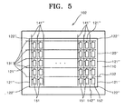
- FIG. 5 is a plan view of the organic light emitting display device 102 according to another embodiment of the invention.
- a plurality of first scan lines 131" and a plurality of first data lines 141" crossing the first scan lines 131" are included in a display unit 120" on a substrate 110.
- at least one second scan line 132", separated from the first scan lines 131", and at least one second data line 142", separated from the first data lines 141 ", are included in the display unit 120".
- a plurality of pixel units 151 are electrically connected to the first scan lines 131" and the first data lines 141 ".
- At least one pixel unit 152 as a pixel unit for testing pixels, typically located at least in a corner 122", or other suitable area, such as a peripheral area 121" which includes the corners 122" of the display unit 120", that is not connected to the first scan lines 131" and the first data lines 141" is electrically connected to the second scan line 132" and the second data line 142".
- the pixel unit 152 that is typically located in a corner 122" of the display unit 120" and electrically connected to the second scan line 132" and the second data line 142" is a pixel unit for testing pixels. Therefore, the pixel unit 152 electrically connected to the second data line 142" can be used to emit light or can test the electrical characteristics of a thin film transistor (TFT) included in the pixel unit 152 by applying an electrical signal to the second scan line 132" and the second data line 142". In this regard, the pixel unit 152, electrically connected to the second scan line 132" and the second data line 142", is located in the display unit 120".
- TFT thin film transistor
- the pixel unit 152 shares the same, similar, or corresponding environment and structure as the pixel units 151 located in the display unit 120". Accordingly, the characteristics of the pixel unit 152 to test pixels are identical, similar or correspond to the characteristics of the pixel units 151 in the display unit 120".
- the pixel unit 152 electrically connected to the second scan line 132" and the second data line 142" typically cannot be used for displaying an image in the display unit 120", but the pixel unit 152 typically does not affect the image quality since the pixel unit 152 is typically located in a corner 122" of the display unit 120".
- the pixel unit 152 electrically connected to the second scan line 132" and the second data line 142" denotes a location where a pixel can be formed.
- a light-emitting display device or element, or an electronic device such as a thin film transistor (TFT) that controls the light-emitting display device can be formed in the pixel unit 152. In the latter case, the pixel unit 152 can be used for testing the characteristics of the electronic device.
- TFT thin film transistor
- An organic light emitting display device can have the following effects or characteristics, for example.
- Second, the pixel unit to test pixels is located in a display unit so that the pixel unit shares the same, similar, or corresponding environment and structure as the pixel units to display images in the display unit. Therefore, a suitable characteristic test of the pixels in a display device can be made according to aspects of the invention.
- the at least one pixel unit to test the pixels is typically located in a corner, or other suitable area, such as a peripheral area which includes the corners, of the display unit, so that the pixel unit, as a pixel unit, typically cannot affect the quality of a displayed image.
Abstract
Description
- Aspects of the invention relate to an organic light-emitting display device, and more particularly, to an organic light-emitting display device having a pixel unit that has the same characteristics as the pixels of the display device and that is used for testing the pixels of the display device.
- An organic light emitting display device is an emissive display device that emits light by energy generated from exitons formed by recombining electrons and holes injected through an anode electrode and a cathode electrode in an organic thin film. The organic light emitting display device can operate at a low voltage, is thin and light, and has a wide viewing angle and a quick response time. Also, studies have been conducted with regard to active matrix (AM) organic light emitting display devices, where light emission or the absence of light emission and the degree of light emission of each pixel are controlled by a thin film transistor (TFT) included in each pixel.
- In manufacturing organic light emitting display devices, tests for checking products, for example, the formation of pixels, the characteristics of a TFT in each pixel, etc., are typically necessary. In the conventional art, as depicted in FIG. 1, a
pixel unit 50 to test the final product is further formed on asubstrate 10 outside adisplay unit 20 to check the formation of pixels and the characteristics of the TFT in the pixel. Thepixel unit 50 denotes a location where a pixel can be formed. Thedisplay unit 20 can include a display device that involves light emission or can include only an electronic device, such as a TFT that controls the display device. - As depicted in FIG. 2, after a test is completed using the
pixel unit 50, thepixel unit 50 can be removed from a final light emitting display device by cutting along a line A-A, as necessary. However, where anadditional pixel unit 50 to test pixels is formed, the surroundings and structure of the pixel in thepixel unit 50 can be different from pixels in thedisplay unit 20. Therefore, the characteristics of the pixel in thepixel unit 50 and the pixels in thedisplay unit 20 are not necessarily identical. Therefore, the reliability of a test result can typically be low. - Aspects of the invention provide an organic light emitting display device having a pixel unit that has the same characteristics as pixels displaying images and which is used for testing the pixels displaying the images.
- According to an aspect of the present invention, there is provided an organic light-emitting display device, including: a substrate; a display unit located on the substrate; a plurality of first scan lines located in the display unit; and a second scan line located in the display unit and separated from the first scan lines, wherein a plurality of pixel units, except one pixel unit located in at least one corner, or other suitable area, of the display unit, are electrically connected to the first scan lines, and the pixel unit that is not connected to the first scan line is electrically connected to the second scan line.
- According to aspects of the invention, the pixel unit electrically connected to the second scan line can be a pixel unit having the characteristics of the pixels displaying images of the display unit for testing pixels of the display unit. The pixel unit electrically connected to the second scan line can include only electronic elements. The electronic elements can include thin film transistors (TFTs).
- According to another aspect of the present invention, there is provided an organic light-emitting display device, including: a substrate; a display unit located in the substrate; a plurality of first data lines located in the display unit; and a second data line located on the display unit and separated from the first data lines, wherein a plurality of pixel units, except one pixel unit located in at least one corner, or other suitable area, of the display unit, are electrically connected to the first date lines, and the pixel unit that is not connected to the first data line is electrically connected to the second data line.
- The pixel unit electrically connected to the second data line can be a pixel unit having the characteristics of the pixels displaying images of the display unit to test pixels of the display unit. The pixel unit electrically connected to the second data line can include only electronic elements. The electronic elements can be only thin film transistors (TFTs).
- According to another aspect of the present invention, there is provided an organic light emitting display device, including: a substrate; a display unit located in the substrate; a plurality of first scan lines located in the display unit; and a second scan line located in the display unit and separated from the plurality of first scan lines; a plurality of first data lines located on the display unit; and a second data line located on the display unit and separated from the first data lines, wherein a plurality of pixel units, except one pixel unit located in at least one corner, or other suitable area, of the display unit, are electrically connected to the first scan lines and the first data lines, and the pixel unit that is not connected to the first scan lines and the first data lines is electrically connected to the second scan line and the second data line.
- The pixel unit electrically connected to the second scan line and the second data line can be a pixel unit having the characteristics of the pixels displaying images of the display unit to test pixels of the display unit. The pixel unit electrically connected to the second scan line and the second data line can include electronic elements. The electronic elements can include thin film transistors (TFTs). The second scan line may be dedicated to the second pixel unit. The second data line may be dedicated to the second pixel unit.
- Additional aspects and/or advantages of the invention are set forth in the description which follows or are evident from the description, or can be learned by practice of the invention.
- These and/or other aspects and advantages of the invention will become apparent and more readily appreciated from the following description of the embodiments, taken in conjunction with the accompanying drawings of which:
- FIG. 1 is a plan view of a conventional organic light emitting display device;
- FIG. 2 is a plan view of another conventional organic light emitting display device;
- FIG. 3 is a plan view of an organic light emitting display device according to an embodiment of the invention;
- FIG. 4 is a plan view of an organic light emitting display device according to another embodiment of the invention; and
- FIG. 5 is a plan view of an organic light emitting display device according to another embodiment of the invention.
- Reference will now be made in detail to embodiments of the invention, examples of which are illustrated in the accompanying drawings, wherein like reference numerals refer to the like elements throughout. The embodiments are described below in order to explain aspects of the invention by referring to the figures, with well-known functions or constructions not necessarily being described in detail.
- FIG. 3 is a plan view of an organic light
emitting display device 100 according to an embodiment of the invention. Referring to FIG. 3, adisplay unit 120 is formed on asubstrate 110. Thedisplay unit 120 includes a plurality ofpixel units pixel units pixel units - The
pixel units substrate 110 can be a glass substrate, a plastic substrate formed of various plastics such as acryl, etc., or a metal substrate, or other suitable substrate, and thesubstrate 110 according to aspects of the invention is therefore not limited in this regard. - The
display unit 120 includes a plurality offirst scan lines 131 and at least onesecond scan line 132 separated from thefirst scan lines 131. Allpixel units 151, except for the at least onepixel unit 152 located on at least onecorner 122, or other suitable area, such as in aperipheral area 121 which includes thecorners 122, of thedisplay unit 120, are electrically connected to thefirst scan lines 131, and thepixel unit 152, which is not electrically connected to thefirst scan lines 131 is electrically connected to thesecond scan line 132. In FIG. 3, at least onepixel unit 152 located in a lowerright corner 122 of thedisplay unit 120 is connected to thesecond scan line 132. Of course, various connection modifications are possible with regard to connecting thepixel units 151 and the at least onepixel unit 152. For example, a plurality of pixel units located in the lowerright corner 122 of thedisplay unit 120 can be connected to thesecond scan line 132, or pixel units located in anothercorner 122 of thedisplay unit 120 can also be connected to thesecond scan line 132. Also, according to aspects of the invention, various connection modifications are also possible for thepixel units 151 and the at least onepixel unit 152 of the organic lightemitting display device 100 of FIG. 3, the organic lightemitting display device 101 of FIG. 4 and the organic lightemitting display device 102 of FIG. 5, or for other embodiments of the invention. - In the organic light
emitting display device 100 of FIG. 3, a plurality ofdata lines 141 crossing thefirst scan lines 131 is formed. Thepixel units 151 and thepixel unit 152 are electrically connected to thedata lines 141. Thepixel units 151 electrically connected to thefirst scan lines 131 and thepixel unit 152 electrically connected to thesecond scan line 132 are organic light emitting elements including a first electrode, a second electrode facing the first electrode, and an intermediate layer interposed between the first electrode and the second electrode and formed of an organic material. The intermediate layer can be formed of multiple layers including at least a light-emitting layer. - The configuration of the organic light-emitting elements, such as the
pixel units 151 and thepixel unit 152, will now be described. The first electrode of the organic light-emitting elements functions as an anode electrode, and the second electrode of the organic light-emitting elements functions as a cathode electrode. The polarity of the first electrode and the second electrode of the organic light-emitting elements can be opposite to each other. - The first electrode of the organic light-emitting elements can be a transparent electrode or a reflection electrode. When the first electrode of the organic light-emitting elements is a transparent electrode, the first electrode can be formed of ITO, IZO, ZnO or In2O3, and where the first electrode of the organic light-emitting elements is a reflection electrode, after a reflection film is formed using Ag, Mg, Al, Pt, Pd, Au, Ni, Nd, Ir, Cr, or a compound of these metals, a film can be formed on the reflection film using ITO, IZO, ZnO or In2O3.
- The second electrode of the organic light-emitting elements can also be a transparent electrode or a reflection electrode. When the second electrode of the organic light-emitting elements is a transparent electrode, after depositing a material layer formed of Li, Ca, LiF/Ca, LiF/Al, Al, Ag, Mg, or a compound of these metals facing the organic film layer interposed between the first electrode and the second electrode of the organic light-emitting elements, an auxiliary electrode or a bus electrode line can be formed using a material for forming the transparent electrode, such as ITO, IZO, ZnO or Zn2O3, on the material layer. Where the second electrode of the organic light-emitting elements is a reflection electrode, the second electrode of the organic light-emitting elements is formed by entirely depositing Li, Ca, LiF/Ca, LiF/Al, Al, Ag, Mg, or a compound of these metals.
- The intermediate layer of the organic light-emitting elements includes at least an emission layer formed between the first electrode and the second electrode of the organic light-emitting elements. The intermediate layer of the organic light-emitting elements can be formed of a low molecular organic material or a polymer organic material.
- Where the intermediate layer of the organic light-emitting elements is formed of a low molecular weight organic material, the intermediate layer of the organic light-emitting elements can be formed in a single or a composite structure by stacking a hole injection layer (HIL), a hole transport layer (HTL), an emission layer (EML), an electron transport layer (ETL), and an electron injection layer (EIL). Organic materials that can be used to form the organic intermediate layer of the organic light-emitting elements can include copper phthalocyanine (CuPc), N,N'-Di(naphthalene-1-yl)-N,N'-diphenyl-benzidine (NPB), and tris-8-hydroxyquinoline aluminium (Alq3). The structure of the intermediate layer of the organic light-emitting elements and the materials to form the intermediate layer of the organic light-emitting elements, according to aspects of the invention, are not limited in this regard. The organic intermediate layer of the organic light-emitting elements can be formed using a vacuum evaporation method using masks, for example.
- When the intermediate layer of the organic light-emitting elements is formed of a polymer organic material, the intermediate layer of the organic light-emitting elements can include a hole transport layer (HTL) and an emission layer (EML). The polymer hole transport layer (HTL) can be formed of poly-(2,4)-ethylene-dihydroxy thiophene (PEDOT) and the polymer organic light emitting layer can be formed of polyphenylenevinylene (PPV) group or polyfluorene group polymer, for example.
- Also, in the organic light emitting
display device 100 of FIG. 3, the organic light-emitting elements, such as thepixel units 151 and thepixel unit 152, formed on thesubstrate 110 can be sealed by a facing member. The facing member can be formed of glass or plastic similar to thesubstrate 110, or other suitable material or composition. The facing member can also be a metal cap, or other suitable cap. - Further, according to aspects of the invention, the exemplary above described structure and composition of the organic light emitting elements in the organic
light emitting display 100 of FIG. 3, including the first electrode, the second electrode the intermediate layer, the facing layer and the cap, can also apply to the structure and composition of the organic light emitting elements, such as thepixel units 151 and the at least onepixel unit 152, of the organic light emittingdisplay device 101 of FIG. 4 and the organic light emittingdisplay device 102 of FIG. 5, or to other embodiments of the invention. - In the organic light emitting
display device 100 of FIG. 3, thepixel unit 152 located in a lowerright corner 122 of thedisplay unit 120 and electrically connected to thesecond scan line 132 is a pixel unit for testing pixels. Therefore, thepixel unit 152 electrically connected to thesecond scan line 132 can be used to emit light, or can test the electrical characteristics of a thin film transistor (TFT) included in thepixel unit 152 by applying an electrical signal to thesecond scan line 132. In this regard, thepixel unit 152 electrically connected to thesecond scan line 132 is located in thedisplay unit 120. Therefore, thepixel unit 152 shares the same, similar, or corresponding environment and structure as thepixel units 151 located in thedisplay unit 120. Accordingly, the characteristics of thepixel unit 152 to test pixels are identical, similar, or correspond to the characteristics of thepixel units 151 in thedisplay unit 120. - The
pixel unit 152, as a pixel unit for testing pixels, electrically connected to thesecond scan line 132, typically cannot be used to display an image in thedisplay unit 120, but thepixel unit 152 typically does not affect the image quality, since thepixel unit 152 is typically located in acorner 122 of thedisplay unit 120. Thepixel unit 152 electrically connected to thesecond scan line 132 denotes a location where a pixel can be formed. Thus, a light-emitting display device or element, or an electronic device such as a thin film transistor (TFT) that controls the light-emitting display device, can be formed in thepixel unit 152. In the latter case, according to aspects of the invention, thepixel unit 152 can be used to test the characteristics of the electronic device. - FIG. 4 is a plan view of the organic light emitting
display device 101 according to another embodiment of the invention. Referring to FIG. 4, a display unit 120' includes a plurality of scan lines 131', a plurality of first data lines 141' and at least one second data line 142' separated from the first data lines 141'. A plurality ofpixel units 151 are electrically connected to the scan lines 131' and the first data lines 141'. At least onepixel unit 152, as a pixel unit, located at least in a corner 122', or other suitable area, such as a peripheral area 121'which includes the corners 122', of the display unit 120', that is not connected to the first data lines 141', is electrically connected to the second data line 142' and to a scan line 131'. - In the organic light emitting
display device 101, thepixel unit 152 located in a lower right corner 122' of the display unit 120' and electrically connected to the second data line 142' is a pixel unit for testing pixels. Therefore, thepixel unit 152 electrically connected to the second data line 142' can be used to emit light, or can test the electrical characteristics of a thin film transistor (TFT) included in thepixel unit 152 by applying an electrical signal to the second data line 142'. In this regard, thepixel unit 152 electrically connected to the second data line 142' is located in the display unit 120'. Therefore, thepixel unit 152 shares the same, similar, or corresponding environment and structure as thepixel units 151 located in the display unit 120'. Accordingly, the characteristics of thepixel unit 152 to test pixels are identical, similar, or correspond to the characteristics of thepixel units 151 in the display unit 120'. - The
pixel unit 152 electrically connected to the second data line 142' typically cannot be used to display an image in the display unit 120', but thepixel unit 152 typically does not affect the image quality, since thepixel unit 152 is typically located in a corner 122' of the display unit 120'. Thepixel unit 152 which is electrically connected to the second data line 142' denotes a location where a pixel can be formed. Thus, a light-emitting display device or element, or an electronic device such as a thin film transistor (TFT) that controls the light-emitting display device, can be formed in thepixel unit 152. In the latter case, according to aspects of the invention, thepixel unit 152 can be used to test the characteristics of the electronic device. - FIG. 5 is a plan view of the organic light emitting
display device 102 according to another embodiment of the invention. Referring to FIG. 5, a plurality offirst scan lines 131" and a plurality offirst data lines 141" crossing thefirst scan lines 131" are included in adisplay unit 120" on asubstrate 110. Also, at least onesecond scan line 132", separated from thefirst scan lines 131", and at least onesecond data line 142", separated from thefirst data lines 141 ", are included in thedisplay unit 120". A plurality ofpixel units 151 are electrically connected to thefirst scan lines 131" and thefirst data lines 141 ". At least onepixel unit 152, as a pixel unit for testing pixels, typically located at least in acorner 122", or other suitable area, such as aperipheral area 121" which includes thecorners 122" of thedisplay unit 120", that is not connected to thefirst scan lines 131" and thefirst data lines 141" is electrically connected to thesecond scan line 132" and thesecond data line 142". - In the organic light emitting
display device 102, thepixel unit 152 that is typically located in acorner 122" of thedisplay unit 120" and electrically connected to thesecond scan line 132" and thesecond data line 142" is a pixel unit for testing pixels. Therefore, thepixel unit 152 electrically connected to thesecond data line 142" can be used to emit light or can test the electrical characteristics of a thin film transistor (TFT) included in thepixel unit 152 by applying an electrical signal to thesecond scan line 132" and thesecond data line 142". In this regard, thepixel unit 152, electrically connected to thesecond scan line 132" and thesecond data line 142", is located in thedisplay unit 120". Therefore, thepixel unit 152 shares the same, similar, or corresponding environment and structure as thepixel units 151 located in thedisplay unit 120". Accordingly, the characteristics of thepixel unit 152 to test pixels are identical, similar or correspond to the characteristics of thepixel units 151 in thedisplay unit 120". - The
pixel unit 152 electrically connected to thesecond scan line 132" and thesecond data line 142" typically cannot be used for displaying an image in thedisplay unit 120", but thepixel unit 152 typically does not affect the image quality since thepixel unit 152 is typically located in acorner 122" of thedisplay unit 120". Thepixel unit 152 electrically connected to thesecond scan line 132" and thesecond data line 142" denotes a location where a pixel can be formed. Thus, a light-emitting display device or element, or an electronic device such as a thin film transistor (TFT) that controls the light-emitting display device, can be formed in thepixel unit 152. In the latter case, thepixel unit 152 can be used for testing the characteristics of the electronic device. - An organic light emitting display device according to aspects of the invention can have the following effects or characteristics, for example. First, at least one pixel unit to test pixels, having the same, similar, or corresponding characteristics and structure as pixel units that display images can be formed. Second, the pixel unit to test pixels is located in a display unit so that the pixel unit shares the same, similar, or corresponding environment and structure as the pixel units to display images in the display unit. Therefore, a suitable characteristic test of the pixels in a display device can be made according to aspects of the invention. Also, according to aspects of the invention, the at least one pixel unit to test the pixels is typically located in a corner, or other suitable area, such as a peripheral area which includes the corners, of the display unit, so that the pixel unit, as a pixel unit, typically cannot affect the quality of a displayed image.
- The foregoing embodiments, aspects and advantages are merely exemplary and are not to be construed as limiting the invention. Also, the description of the embodiments of the invention is intended to be illustrative, and not to limit the scope of the claims, and various other alternatives, modifications, and variations will be apparent to those skilled in the art. Therefore, although a few embodiments of the invention have been shown and described, it would be appreciated by those skilled in the art that changes may be made in the embodiments without departing from the scope of the invention, which is defined in the claims and their equivalents.
Claims (10)
- An organic light-emitting display device, comprising:a substrate;a display unit located on the substrate;a plurality of first scan lines;a second scan line separated from the first scan lines,a plurality of first pixel units located in the display unit, and electrically connected to the first scan lines; anda second pixel unit located in the display unit;wherein the second pixel unit is not connected to the first scan lines and is electrically connected to the second scan line.
- An organic light-emitting display device, comprising:a substrate;a display unit located on the substrate;a plurality of first data lines;a second data line separated from the first data lines,a plurality of first pixel units located in the display unit and electrically connected to the first data lines; anda second pixel unit located in the display unit,wherein the second pixel unit is not connected to the first data lines and is electrically connected to the second data line.
- An organic light-emitting display device according to claim 1 further, comprising:a plurality of first data lines; anda second data line separated from the first data lines, whereinthe plurality of first pixel units, are electrically connected to the first data lines, andthe second pixel unit is not connected to the first data lines and is electrically connected to the second data line.
- An organic light-emitting display device according to any one of claims 1 to 3, wherein:the second pixel unit comprises a pixel unit for testing the plurality of first pixel units.
- An organic light-emitting display device according to any one of claims 1 to 4, wherein:the second pixel unit comprises electronic elements.
- An organic light-emitting display device according to claim 5, wherein:the electronic elements comprise thin film transistors (TFTs).
- An organic light-emitting display device according to any one of claims 1 to 6, wherein:the said pixel unit has characteristics corresponding to characteristics of the plurality of pixel units.
- An organic light-emitting display device, according to any preceding claim:
wherein the second pixel unit is located in a peripheral area of the display unit. - An organic light-emitting display device according to claim 8, wherein:the peripheral area comprises at least one corner of the display unit.
- An organic light-emitting display device according to any preceding claim, wherein:the second pixel unit has a corresponding environment and structure to the plurality of first pixel units.
Applications Claiming Priority (1)
| Application Number | Priority Date | Filing Date | Title |
|---|---|---|---|
| KR1020050092145A KR100708715B1 (en) | 2005-09-30 | 2005-09-30 | Organic light emitting display apparatus |
Publications (1)
| Publication Number | Publication Date |
|---|---|
| EP1770680A1 true EP1770680A1 (en) | 2007-04-04 |
Family
ID=37684508
Family Applications (1)
| Application Number | Title | Priority Date | Filing Date |
|---|---|---|---|
| EP06255080A Ceased EP1770680A1 (en) | 2005-09-30 | 2006-09-29 | Organic light-emitting display device having a pixel unit for testing pixels of the display device |
Country Status (3)
| Country | Link |
|---|---|
| US (1) | US8223095B2 (en) |
| EP (1) | EP1770680A1 (en) |
| KR (1) | KR100708715B1 (en) |
Cited By (1)
| Publication number | Priority date | Publication date | Assignee | Title |
|---|---|---|---|---|
| CN108806602A (en) * | 2013-05-31 | 2018-11-13 | 三星显示有限公司 | Organic light emitting display panel |
Families Citing this family (8)
| Publication number | Priority date | Publication date | Assignee | Title |
|---|---|---|---|---|
| JP2008211146A (en) * | 2007-02-28 | 2008-09-11 | Oki Data Corp | Information display device |
| KR101365898B1 (en) * | 2007-05-16 | 2014-02-24 | 엘지디스플레이 주식회사 | Organic light emitting device |
| KR20100130008A (en) * | 2009-06-02 | 2010-12-10 | 삼성전자주식회사 | Sollar cell structure |
| US8259095B2 (en) * | 2009-08-20 | 2012-09-04 | Global Oled Technology Llc | Optically testing chiplets in display device |
| KR101954981B1 (en) | 2010-09-24 | 2019-03-08 | 삼성디스플레이 주식회사 | Organic light emitting display device |
| KR102047002B1 (en) * | 2013-05-31 | 2019-11-21 | 삼성디스플레이 주식회사 | Organic light emitting display apparatus and method for repair thereof |
| CN103761935B (en) * | 2014-01-21 | 2016-01-06 | 深圳市华星光电技术有限公司 | Display panel |
| CN108305576B (en) * | 2017-01-13 | 2021-11-30 | 元太科技工业股份有限公司 | Display device |
Citations (5)
| Publication number | Priority date | Publication date | Assignee | Title |
|---|---|---|---|---|
| EP1341147A2 (en) * | 2002-02-27 | 2003-09-03 | Tohoku Pioneer Corp. | Drive method of light-emitting display and organic EL display device |
| EP1450341A1 (en) * | 2001-09-25 | 2004-08-25 | Matsushita Electric Industrial Co., Ltd. | El display panel and el display apparatus comprising it |
| WO2004088626A1 (en) * | 2003-04-01 | 2004-10-14 | Koninklijke Philips Electronics N.V. | Active matrix display devices with modelling circuit located outside the display area for compensating threshold variations of the pixel drive transistor |
| WO2004097782A1 (en) * | 2003-05-02 | 2004-11-11 | Koninklijke Philips Electronics N.V. | Active matrix oled display device with threshold voltage drift compensation |
| US20040263445A1 (en) * | 2001-01-29 | 2004-12-30 | Semiconductor Energy Laboratory Co., Ltd, A Japan Corporation | Light emitting device |
Family Cites Families (2)
| Publication number | Priority date | Publication date | Assignee | Title |
|---|---|---|---|---|
| JP3928413B2 (en) * | 2001-11-15 | 2007-06-13 | ソニー株式会社 | Image display device driving method and image display device |
| JP4610886B2 (en) * | 2002-12-06 | 2011-01-12 | 株式会社半導体エネルギー研究所 | Image display device, electronic equipment |
-
2005
- 2005-09-30 KR KR1020050092145A patent/KR100708715B1/en active IP Right Grant
-
2006
- 2006-08-21 US US11/506,828 patent/US8223095B2/en active Active
- 2006-09-29 EP EP06255080A patent/EP1770680A1/en not_active Ceased
Patent Citations (5)
| Publication number | Priority date | Publication date | Assignee | Title |
|---|---|---|---|---|
| US20040263445A1 (en) * | 2001-01-29 | 2004-12-30 | Semiconductor Energy Laboratory Co., Ltd, A Japan Corporation | Light emitting device |
| EP1450341A1 (en) * | 2001-09-25 | 2004-08-25 | Matsushita Electric Industrial Co., Ltd. | El display panel and el display apparatus comprising it |
| EP1341147A2 (en) * | 2002-02-27 | 2003-09-03 | Tohoku Pioneer Corp. | Drive method of light-emitting display and organic EL display device |
| WO2004088626A1 (en) * | 2003-04-01 | 2004-10-14 | Koninklijke Philips Electronics N.V. | Active matrix display devices with modelling circuit located outside the display area for compensating threshold variations of the pixel drive transistor |
| WO2004097782A1 (en) * | 2003-05-02 | 2004-11-11 | Koninklijke Philips Electronics N.V. | Active matrix oled display device with threshold voltage drift compensation |
Cited By (1)
| Publication number | Priority date | Publication date | Assignee | Title |
|---|---|---|---|---|
| CN108806602A (en) * | 2013-05-31 | 2018-11-13 | 三星显示有限公司 | Organic light emitting display panel |
Also Published As
| Publication number | Publication date |
|---|---|
| US8223095B2 (en) | 2012-07-17 |
| US20070075936A1 (en) | 2007-04-05 |
| KR100708715B1 (en) | 2007-04-17 |
| KR20070036995A (en) | 2007-04-04 |
Similar Documents
| Publication | Publication Date | Title |
|---|---|---|
| US8223095B2 (en) | Organic light-emitting display device having a pixel unit for testing pixels of the display device | |
| US9647046B2 (en) | Organic light emitting diode display having high aperture ratio and method for manufacturing the same | |
| US7510891B2 (en) | Organic light emitting display device and method of manufacturing the same | |
| US11443695B2 (en) | Display apparatus | |
| US20150048335A1 (en) | Organic light-emitting display apparatus and method of manufacturing the same | |
| US8550667B2 (en) | Optical film and organic light emitting display apparatus including the same | |
| JP2016146364A (en) | Organic light emitting display device | |
| KR102443645B1 (en) | Organic light emitting diode display and manufacturing method thereof | |
| US8927327B2 (en) | Method of manufacturing organic light emitting display device having polarizable particles in sealant | |
| US9331131B2 (en) | Organic light emitting diode display and manufacturing method thereof | |
| US20140138630A1 (en) | Organic light-emitting display apparatus and method of manufacturing the same | |
| US20230178036A1 (en) | Display apparatus | |
| US9185796B2 (en) | Organic light emitting diode display and manufacuring method thereof | |
| KR101694886B1 (en) | Image display apparatus and organic light emitting display apparatus comprising image shift unit | |
| US9269756B2 (en) | Organic light emitting display apparatus | |
| US20210005700A1 (en) | Display apparatus | |
| US9224986B2 (en) | Organic light-emitting display device and method of manufacturing same | |
| KR102324765B1 (en) | Organic light emitting diode display and method of manufacturing the same | |
| KR20220044173A (en) | Display panel and display apparatus including the same | |
| US8395145B2 (en) | Top-emitting organic light-emitting device | |
| KR100787454B1 (en) | Organic light emitting display apparatus | |
| KR100626078B1 (en) | Method of detecting and repairing shorted portion in flat panel display | |
| US11594560B2 (en) | Display apparatus | |
| KR100741134B1 (en) | Organic light emitting display apparatus | |
| KR100669740B1 (en) | Flat display device |
Legal Events
| Date | Code | Title | Description |
|---|---|---|---|
| PUAI | Public reference made under article 153(3) epc to a published international application that has entered the european phase |
Free format text: ORIGINAL CODE: 0009012 |
|
| 17P | Request for examination filed |
Effective date: 20061006 |
|
| AK | Designated contracting states |
Kind code of ref document: A1 Designated state(s): AT BE BG CH CY CZ DE DK EE ES FI FR GB GR HU IE IS IT LI LT LU LV MC NL PL PT RO SE SI SK TR |
|
| AX | Request for extension of the european patent |
Extension state: AL BA HR MK YU |
|
| AKX | Designation fees paid |
Designated state(s): DE FR GB |
|
| RAP1 | Party data changed (applicant data changed or rights of an application transferred) |
Owner name: SAMSUNG MOBILE DISPLAY CO., LTD. |
|
| 17Q | First examination report despatched |
Effective date: 20090211 |
|
| RAP1 | Party data changed (applicant data changed or rights of an application transferred) |
Owner name: SAMSUNG DISPLAY CO., LTD. |
|
| STAA | Information on the status of an ep patent application or granted ep patent |
Free format text: STATUS: THE APPLICATION HAS BEEN REFUSED |
|
| 18R | Application refused |
Effective date: 20130115 |