EP1769264B1 - Bulk material windows for distributed aperture sensors - Google Patents
Bulk material windows for distributed aperture sensors Download PDFInfo
- Publication number
- EP1769264B1 EP1769264B1 EP05756302A EP05756302A EP1769264B1 EP 1769264 B1 EP1769264 B1 EP 1769264B1 EP 05756302 A EP05756302 A EP 05756302A EP 05756302 A EP05756302 A EP 05756302A EP 1769264 B1 EP1769264 B1 EP 1769264B1
- Authority
- EP
- European Patent Office
- Prior art keywords
- window
- sensor system
- ohm
- windows
- test
- Prior art date
- Legal status (The legal status is an assumption and is not a legal conclusion. Google has not performed a legal analysis and makes no representation as to the accuracy of the status listed.)
- Revoked
Links
- 239000013590 bulk material Substances 0.000 title 1
- 238000000034 method Methods 0.000 claims abstract description 10
- 229910052710 silicon Inorganic materials 0.000 claims description 16
- 239000010703 silicon Substances 0.000 claims description 16
- 230000005670 electromagnetic radiation Effects 0.000 claims description 2
- 230000003287 optical effect Effects 0.000 claims 2
- 239000000463 material Substances 0.000 abstract description 18
- 238000012360 testing method Methods 0.000 description 39
- XUIMIQQOPSSXEZ-UHFFFAOYSA-N Silicon Chemical compound [Si] XUIMIQQOPSSXEZ-UHFFFAOYSA-N 0.000 description 14
- 239000000758 substrate Substances 0.000 description 12
- 238000003780 insertion Methods 0.000 description 9
- 230000037431 insertion Effects 0.000 description 9
- 238000005259 measurement Methods 0.000 description 9
- 230000005540 biological transmission Effects 0.000 description 7
- 238000004519 manufacturing process Methods 0.000 description 7
- 229910003460 diamond Inorganic materials 0.000 description 5
- 239000010432 diamond Substances 0.000 description 5
- 230000010287 polarization Effects 0.000 description 5
- 238000009304 pastoral farming Methods 0.000 description 4
- PXHVJJICTQNCMI-UHFFFAOYSA-N Nickel Chemical compound [Ni] PXHVJJICTQNCMI-UHFFFAOYSA-N 0.000 description 2
- 238000009434 installation Methods 0.000 description 2
- 238000012986 modification Methods 0.000 description 2
- 230000004048 modification Effects 0.000 description 2
- 238000012935 Averaging Methods 0.000 description 1
- RYGMFSIKBFXOCR-UHFFFAOYSA-N Copper Chemical compound [Cu] RYGMFSIKBFXOCR-UHFFFAOYSA-N 0.000 description 1
- 241001074085 Scophthalmus aquosus Species 0.000 description 1
- 229910052782 aluminium Inorganic materials 0.000 description 1
- XAGFODPZIPBFFR-UHFFFAOYSA-N aluminium Chemical compound [Al] XAGFODPZIPBFFR-UHFFFAOYSA-N 0.000 description 1
- 238000004458 analytical method Methods 0.000 description 1
- 229910052799 carbon Inorganic materials 0.000 description 1
- 238000012512 characterization method Methods 0.000 description 1
- 229910052802 copper Inorganic materials 0.000 description 1
- 239000010949 copper Substances 0.000 description 1
- 238000013480 data collection Methods 0.000 description 1
- 238000010586 diagram Methods 0.000 description 1
- 230000008030 elimination Effects 0.000 description 1
- 238000003379 elimination reaction Methods 0.000 description 1
- 238000011156 evaluation Methods 0.000 description 1
- 230000003993 interaction Effects 0.000 description 1
- 238000003913 materials processing Methods 0.000 description 1
- 229910052751 metal Inorganic materials 0.000 description 1
- 239000002184 metal Substances 0.000 description 1
- 230000003278 mimic effect Effects 0.000 description 1
- 229910052759 nickel Inorganic materials 0.000 description 1
- 239000003973 paint Substances 0.000 description 1
- 238000012545 processing Methods 0.000 description 1
- 230000003595 spectral effect Effects 0.000 description 1
Images


Classifications
-
- H—ELECTRICITY
- H01—ELECTRIC ELEMENTS
- H01Q—ANTENNAS, i.e. RADIO AERIALS
- H01Q21/00—Antenna arrays or systems
- H01Q21/28—Combinations of substantially independent non-interacting antenna units or systems
Definitions
- the present invention relates to windows for distributed aperture sensors.
- Distributed aperture sensors comprise a collection of sensors mounted either around a vehicle or co-located in one location where an unobstructed 360 degree line-of-sight (or other field of view requiring more than one sensor aperture) can be obtained.
- Each aperture will ordinarily comprise a window.
- the present invention recognized that these bulk materials exhibit performance properties that make them candidates for a lower cost replacement for the epitaxial layer equipped window substrates for distributed aperture sensor windows. Results indicate that a simple, scaleable, readily available, cost and performance effective alternative exists to the traditional expensive, complex, multi-layer applications currently implemented.
- WO 02/101774 A2 discloses an infrared segmented RF signature managed window having at least two surfaces oriented relative to each other at an angle greater than zero.
- the present invention is of a sensor system and method comprising: employing a window comprising a material with a bulk resistivity that is substantially uniform throughout the Window; and sensing electromagnetic radiation through the window.
- the window consists substantially of the material, and most preferably consists of the material.
- the window preferably lacks an epitaxial layer and is a component of a distributed aperture sensor system or radar system.
- the bulk resistivity is preferably less than or equal to approximately 10 ohm-cm, more preferably less than or equal to approximately 5 ohm-cm, and most preferably wherein the window is approximately 0.635 cm thick.
- the material preferably comprises silicon.
- the present invention is also of a window for a sensor system comprising a material with a bulk resistivity that is substantially uniform throughout the window.
- the present invention is of a window for a distributed aperture sensor (or single aperture sensor, though this is less preferred) comprising a material with a bulk resistivity that is substantially uniform throughout the window.
- the preferred material is silicon, and the preferred bulk resistivity is less than 10 ohm-cm, most preferably less than 5 ohm-cm (particularly for a silicon window of 0.635 cm thickness).
- the window consists substantially of such material, and most preferably the window consists of such material.
- the invention is also of a corresponding method and sensor system.
- a preferred distributed aperture sensor system 10 comprises a plurality of sensors 12 each with a window 14 of the invention.
- Two sample window substrates consisting of various characteristic and substantially uniform bulk resistivities were compared to a known measured baseline substrate equipped with a high conductivity epitaxial overlay.
- the sample substrates were manufactured to the same shape and tolerances as a baseline windowpane. All the items were then subsequently mounted in the same test fixture for measurement purposes. Radar cross-section and insertion loss measurements were then performed under identical conditions.
- the radar cross section testing of the silicon window substrates compared the backscatter produced at the window/frame interface to a typical production-type configuration window with an epitaxial (Epi) layer on its top surface.
- Epi epitaxial
- the main area of interest for this test was the backscatter produced by the window/frame interface at near grazing incidence angles.
- IR spectral transmission measurements were also performed on each of the substrates to determine the relative impact of bulk loading on transmission.
- Results,of the RCS characterization measurements indicate that there is a range of bulk volume resistivities within which the RCS performance closely matches that of the substrate containing the high conductivity epitaxial layer. Measurements of insertion loss for each of the substrates demonstrated consistent and similar performance characteristics. Results of the IR transmission measurements indicate nearly identical transmission performance for each of the substrates.
- the window substrate chosen to serve as the baseline for this evaluation has 0.0698 m (2.75") long, straight leading edges at angles of 29° and 31° relative to the window's long axis.
- a production configuration bezel was machined into a 0.00635 m (0.25") thick, T6 aluminum, removable test coupon panel. It was located forward of the center of rotation and at an angle of 60° relative to the diamond's long axis radially outward from the center as far as possible to enhance movement of the window when the test body is rotated in azimuth.
- Fig. 2 provides a top view of the test coupon panel with the windows and bezel placement. Note that at 0° azimuth, the window's longest edges are facing forward toward the RF emitter.
- a 151 tap FIR Doppler filter was used to remove stationary scatterers, i.e. pylon, test body to pylon interactions, test chamber noise, etc., from the measured backscatter to reduce the background which tends to be higher in W polarization (transmitter and receiver vertically polarized).
- W polarization transmitter and receiver vertically polarized
- the entire diamond test coupon panel was nickel plated on both sides to mimic a window frame and all three windows were test fitted into the bezel and profiled to insure that they met a step requirement of +0.13/-0,10 mm (+5/-4 mils).
- the average step height for the three windows as tested were:
- range gate was set at 122 cm to eliminate scattering from the test body's leading and trailing tips and that backscatter data was collected for grazing incidence angles of 1°, 10° and 15°.
- the measurement system was calibrated for RCS data collection using a six (6) inch diameter metallic sphere (-17.4 dB sm ).
- One baseline configuration was tested: a standard production configuration silicon window with Epi layer that met typical specifications for such windows. Backscatter from this window's interface region, window/AI knife edge, is the reference backscatter level for comparison with that produced by the two bulk silicon test windows. Two different resistivity windows according to the invention, 2 and 10 ohm-cm, were installed into the test coupon panel and the resulting backscatter was measured and compared to the baseline configuration to determine any increase in backscatter due to the use of the non-Epi layer windows.
- test equipment was used for this test. Equivalent test equipment could have been substituted if needed. Measurement test equipment was certified to be within calibration and of the required accuracy to fulfill the needs of these tests.
- Fig. 4 shows the measured RF transmission levels for both the 10 ohm-cm and 2 ohm-cm windows and the measured level for the production window.
- the present invention permits the elimination of the epitaxial layer and re-specification of silicon window substrates to have a bulk volume resistivity of 5 ohm-cm or less.
- Backscatter levels from a 5 ohm-cm simple silicon window were not evaluated during this test but based upon the levels observed from the 10 and 2 ohm-cm windows, backscatter produced by a 5 ohm-cm window should be acceptable.
Landscapes
- Radar Systems Or Details Thereof (AREA)
- Photometry And Measurement Of Optical Pulse Characteristics (AREA)
- Burglar Alarm Systems (AREA)
- Glass Compositions (AREA)
- Special Wing (AREA)
- Light Receiving Elements (AREA)
Abstract
Description
- The present invention relates to windows for distributed aperture sensors.
- Distributed aperture sensors comprise a collection of sensors mounted either around a vehicle or co-located in one location where an unobstructed 360 degree line-of-sight (or other field of view requiring more than one sensor aperture) can be obtained. Each aperture will ordinarily comprise a window.
- The electromagnetic (EM) capabilities of different window materials and resistivities play an important role in the EM compatibility of host vehicles and the performance of on-board sensors. In the mid-wave infrared, there is a trade between high and low bulk resistivity silicon (Si) windows. The former provides high transmission for optimal sensor performance, while the latter provides increased conductance for low radar cross sections (RCS). In the past, a relatively expensive compromise was utilized to provide the benefits of both types of materials by overlaying the bulk Si substrate material with a low resistivity epitaxial layer. These materials represented a major cost and schedule impact due to the number of steps and amount of material processing, the high degree of precision and the tolerances that had to be maintained, and the requirement for special handling and tools necessary for producing the finished product.
- Recent advances in materials processing, however, have made available materials that can be better tuned for bulk resistivity. These bulk materials are readily available and can be readily provided at a substantially lower cost.
- The present invention recognized that these bulk materials exhibit performance properties that make them candidates for a lower cost replacement for the epitaxial layer equipped window substrates for distributed aperture sensor windows. Results indicate that a simple, scaleable, readily available, cost and performance effective alternative exists to the traditional expensive, complex, multi-layer applications currently implemented.
-
WO 02/101774 A2 - The present invention is of a sensor system and method comprising: employing a window comprising a material with a bulk resistivity that is substantially uniform throughout the Window; and sensing electromagnetic radiation through the window. In the preferred embodiment, the window consists substantially of the material, and most preferably consists of the material. The window preferably lacks an epitaxial layer and is a component of a distributed aperture sensor system or radar system. The bulk resistivity is preferably less than or equal to approximately 10 ohm-cm, more preferably less than or equal to approximately 5 ohm-cm, and most preferably wherein the window is approximately 0.635 cm thick. The material preferably comprises silicon.
- The present invention is also of a window for a sensor system comprising a material with a bulk resistivity that is substantially uniform throughout the window.
- Objects, advantages and novel features, and further scope of applicability of the present invention will be set forth in part in the detailed description to follow, taken in conjunction with the accompanying drawings, and in part will become apparent to those skilled in the art upon examination of the following, or may be learned by practice of the invention. The objects and advantages of the invention may be realized and attained by means of the instrumentalities and combinations particularly pointed out in the appended claims.
- The accompanying drawings, which are incorporated into and form a part of the specification, illustrate one or more embodiments of the present invention and, together with the description, serve to explain the principles of the invention. The drawings are only for the purpose of illustrating one or more preferred embodiments of the invention and are not to be construed as limiting the invention. In the drawings:
-
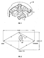
Fig. 1 is a cut-away view of a distributed aperture sensor system comprising windows according to the invention; -
Fig. 2 is a diagram of the test coupon panel with window bezel of the example; -
Fig. 3 is a chart comparing backscatter sector averages for prior art windows and windows according to the invention with 10 ohm-cm and 2 ohm-cm bulk resistivities; -
Fig. 4 is a graph comparing insertion loss in the windows ofFig. 3 ; and -
Fig. 5 is a graph comparing insertion loss in a 0.635 cm thick bulk silicon window at 9 ohm-cm and 5 ohm-cm compared to a preferred maximum. - The present invention is of a window for a distributed aperture sensor (or single aperture sensor, though this is less preferred) comprising a material with a bulk resistivity that is substantially uniform throughout the window. The preferred material is silicon, and the preferred bulk resistivity is less than 10 ohm-cm, most preferably less than 5 ohm-cm (particularly for a silicon window of 0.635 cm thickness). Preferably the window consists substantially of such material, and most preferably the window consists of such material. The invention is also of a corresponding method and sensor system.
- As shown in
Fig. 1 , a preferred distributedaperture sensor system 10 according to the invention comprises a plurality ofsensors 12 each with awindow 14 of the invention. - The invention is further illustrated by the following non-limiting examples.
- Two sample window substrates consisting of various characteristic and substantially uniform bulk resistivities were compared to a known measured baseline substrate equipped with a high conductivity epitaxial overlay. The sample substrates were manufactured to the same shape and tolerances as a baseline windowpane. All the items were then subsequently mounted in the same test fixture for measurement purposes. Radar cross-section and insertion loss measurements were then performed under identical conditions. The radar cross section testing of the silicon window substrates compared the backscatter produced at the window/frame interface to a typical production-type configuration window with an epitaxial (Epi) layer on its top surface. The main area of interest for this test was the backscatter produced by the window/frame interface at near grazing incidence angles. IR spectral transmission measurements were also performed on each of the substrates to determine the relative impact of bulk loading on transmission.
- Results,of the RCS characterization measurements indicate that there is a range of bulk volume resistivities within which the RCS performance closely matches that of the substrate containing the high conductivity epitaxial layer. Measurements of insertion loss for each of the substrates demonstrated consistent and similar performance characteristics. Results of the IR transmission measurements indicate nearly identical transmission performance for each of the substrates.
- To evaluate the near grazing incidence backscatter produced by the Si window / Al frame interface, a very low RCS at grazing incidence test fixture was chosen. This test body, a 1.828 m (6 ft.) model, features a top, center mounted, diamond shaped test coupon panel into which is inserted the window under test. The RCS tests were conducted using a 6.096 m (20-foot) tall, low RCS pylon / Az over El rotator system. A range of 13.176 m (45 feet) exists between the radar antennas and the pylon / rotator location. The rotator provides 360.0 degrees of azimuth rotation at elevation angles of interest.
- The window substrate chosen to serve as the baseline for this evaluation has 0.0698 m (2.75") long, straight leading edges at angles of 29° and 31° relative to the window's long axis. A production configuration bezel was machined into a 0.00635 m (0.25") thick, T6 aluminum, removable test coupon panel. It was located forward of the center of rotation and at an angle of 60° relative to the diamond's long axis radially outward from the center as far as possible to enhance movement of the window when the test body is rotated in azimuth.
Fig. 2 provides a top view of the test coupon panel with the windows and bezel placement. Note that at 0° azimuth, the window's longest edges are facing forward toward the RF emitter. - A 151 tap FIR Doppler filter was used to remove stationary scatterers, i.e. pylon, test body to pylon interactions, test chamber noise, etc., from the measured backscatter to reduce the background which tends to be higher in W polarization (transmitter and receiver vertically polarized). After the diamond test coupon panel was placed in the test body, its edges were taped with metallic tape and the tape was painted with a conductive copper paint similar to that used on the test body's surface.
- The entire diamond test coupon panel was nickel plated on both sides to mimic a window frame and all three windows were test fitted into the bezel and profiled to insure that they met a step requirement of +0.13/-0,10 mm (+5/-4 mils). The average step height for the three windows as tested were:
- Production Baseline: -0.06 mm (-2.2 mils);
- 10 ohm-cm window: -0.07 mm (-2.7 mils); and
- 2 ohm-cm window: +0.02 mm (+0.6 mils).
- The RCS tests were conducted using the parameters in Table 1. The range gate was centered about the 6' test body's center of rotation.
Table 1: RCS Test Parameters Parameter Specification Frequency X band 10 GHz Ku band 16 GHz Polarization HH W Range Gate 1.22 meters (4 feet) Pitch 1 °, +10°, +15° Azimuth Continuous -50° to +50° steps of 0.1° - Note that the range gate was set at 122 cm to eliminate scattering from the test body's leading and trailing tips and that backscatter data was collected for grazing incidence angles of 1°, 10° and 15°.
- The measurement system was calibrated for RCS data collection using a six (6) inch diameter metallic sphere (-17.4 dBsm).
- One baseline configuration was tested: a standard production configuration silicon window with Epi layer that met typical specifications for such windows. Backscatter from this window's interface region, window/AI knife edge, is the reference backscatter level for comparison with that produced by the two bulk silicon test windows. Two different resistivity windows according to the invention, 2 and 10 ohm-cm, were installed into the test coupon panel and the resulting backscatter was measured and compared to the baseline configuration to determine any increase in backscatter due to the use of the non-Epi layer windows.
- All tests were conducted at ambient conditions of temperature, humidity, and pressure prevailing at the test facility at the time the testing was performed.
- The following test equipment was used for this test. Equivalent test equipment could have been substituted if needed. Measurement test equipment was certified to be within calibration and of the required accuracy to fulfill the needs of these tests.
- A. HP8510C Network Analyzer
- B. RF Synthesized Sources: HP8341 B and HP83622B
- C. HP8517B Test Set
- D. S, C and X through Ku band TWTA amplifiers
- E. EM Systems A6100 Feedhorns, One for Transmit and One for Receive
- F. IBM PC with Compu-Quest 1519 Collection and Analysis System V1.23 Software
- No measurable backscatter was observed at the window location in HH polarization for all three windows and for all test configurations. In W polarization, backscatter was observed and the downrange versus azimuth images were used to determine the location and width of the scattering produced by the window's leading edges. Arithmetic sector averages encompassing these two scattering centers were utilized to perform the backscatter comparison of the three windows. The right and left sectors were averaged independently, their average taken and then converted into dBsm to arrive at a single backscatter level at each elevation angle for the window. In X band, the window leading edge scattering occurs over a wider angular sector than in Ku band so, in X band, wider sectors were used for the averaging.
Fig. 3 presents a summary of the W polarization, sector averaged backscatter data for the three windows in each frequency band and at each elevation angle. As can be seen, backscatter from all three windows is less than -43 dBsm except for the 10 ohm-cm window in Ku band at 10° and 15° elevation angles. Table 2 gives the elevation averaged, measured backscatter difference between the 10 and 2 ohm-cm windows and the production configuration window.Table 2: Backscatter Difference Between Simple Si Windows and Production Window Test Window X Band Backscatter Increase Ku Band Backscatter Increase 10 ohm-cm Silicon 1.4 dBsm 4.2 dBsm 2 ohm-cm Silicon 0.2 dBsm 0.5 dBsm - Before the window was removed from the test coupon panel, its RF insertion loss was measured in a transmission tunnel. Due to the window dimensions, this data is only valid from approximately 10 GHz and up. Also, since the windows were not potted into the bezel for this test but just metal taped around their perimeter on the underside of the diamond panel, more RF leakage occurred than would be expected in an actual window installation.
Fig. 4 shows the measured RF transmission levels for both the 10 ohm-cm and 2 ohm-cm windows and the measured level for the production window. - Increase in backscatter over the production configuration window due to use of the 2 ohm-cm simple silicon window is insignificant and within measurement error. The RF insertion loss provided by the 2 ohm-cm window far exceeds current typical requirements. On the other hand, backscatter from the 10 ohm-cm window is 2 to 4 dBsm higher which may not be very significant in an actual detector installation. An Si window resistivity of 5 ohm-cm or less at a thickness of 0.635 cm +/- 0.0127 cm is preferred to provide adequate insertion toss as indicated in
Fig. 5 . This figure shows the insertion loss attainable by using the current typical allowable range for the silicon window's volume resistivity (5 to 9 ohm-cm) along with the insertion loss performance specification for the window. Accordingly, the present invention permits the elimination of the epitaxial layer and re-specification of silicon window substrates to have a bulk volume resistivity of 5 ohm-cm or less. Backscatter levels from a 5 ohm-cm simple silicon window were not evaluated during this test but based upon the levels observed from the 10 and 2 ohm-cm windows, backscatter produced by a 5 ohm-cm window should be acceptable. - Although the invention has been described in detail with particular reference to these preferred embodiments, other embodiments can achieve the same results. Variations and modifications of the present invention will be obvious to those skilled in the art and it is intended to cover in the appended claims all such modifications.
Claims (14)
- A method for sensing electromagnetic radiation through a plurality of windows (14) of a distributed aperture sensor system (10), the method employing a plurality of windows (14) that provide electromagnetic interference shielding characterized by the windows (14) having a bulk resistivity of less than or approximately equal to 10 ohm-cm which is substantially uniform throughout each window (14).
- The method of claim 1 wherein each window (14) lacks an epitaxial layer.
- The method of claim 1 wherein the distributed aperture sensor system (10) is an electro optical system.
- The method of claim 1 wherein the bulk resistivity is less than or equal to approximately 5 ohm-cm.
- The method of claim 1 wherein each window (14) is approximately 0.635 cm thick.
- The method of claim 1 wherein each window (14) comprises silicon.
- A distributed aperture sensor system (10) having a window (14) providing electromagnetic shielding properties characterized by a bulk resistivity of less than or approximately equal to 10 ohm-cm which is substantially uniform throughout said window (14).
- The sensor system (10) of claim 7 wherein in the bulk resistivity is less than or equal to approximately 5 ohm-cm.
- The sensor system (10) of claim 7 wherein said window (14) comprises silicon.
- The sensor system (10) of claim 7 wherein each of said plurality of sensors (12) is an infrared sensor.
- The sensor system (10) of claim 7 wherein the sensor system (10) is an infrared sensor system
- The sensor system (10) of claim 7 wherein said window (14) lacks an epitaxial layer.
- The sensor system (10) of claim 7 wherein each of said plurality of sensors (12) is an electro optical sensor.
- The sensor system (10) of claim 7 wherein each said window (14) is approximately 0.635 cm thick.
Applications Claiming Priority (2)
| Application Number | Priority Date | Filing Date | Title |
|---|---|---|---|
| US10/861,005 US7718936B2 (en) | 2004-06-03 | 2004-06-03 | Bulk material windows for distributed aperture sensors |
| PCT/US2005/019818 WO2005119292A2 (en) | 2004-06-03 | 2005-06-03 | Bulk material windows for distributed aperture sensors |
Publications (3)
| Publication Number | Publication Date |
|---|---|
| EP1769264A2 EP1769264A2 (en) | 2007-04-04 |
| EP1769264A4 EP1769264A4 (en) | 2008-09-10 |
| EP1769264B1 true EP1769264B1 (en) | 2010-08-04 |
Family
ID=35447102
Family Applications (1)
| Application Number | Title | Priority Date | Filing Date |
|---|---|---|---|
| EP05756302A Revoked EP1769264B1 (en) | 2004-06-03 | 2005-06-03 | Bulk material windows for distributed aperture sensors |
Country Status (7)
| Country | Link |
|---|---|
| US (1) | US7718936B2 (en) |
| EP (1) | EP1769264B1 (en) |
| AT (1) | ATE476674T1 (en) |
| AU (1) | AU2005250942B2 (en) |
| CA (1) | CA2565702C (en) |
| DE (1) | DE602005022719D1 (en) |
| WO (1) | WO2005119292A2 (en) |
Family Cites Families (16)
| Publication number | Priority date | Publication date | Assignee | Title |
|---|---|---|---|---|
| US562935A (en) * | 1896-06-30 | sweet | ||
| US4006356A (en) * | 1961-10-27 | 1977-02-01 | Aeronutronic Ford Corporation | Radiant energy tracking device |
| US3912859A (en) * | 1962-06-08 | 1975-10-14 | Philco Ford Corp | Electronic tracking device |
| US3944167A (en) * | 1973-08-24 | 1976-03-16 | Sanders Associates, Inc. | Radiation detection apparatus |
| US5259570A (en) * | 1974-08-12 | 1993-11-09 | The United States Of America As Represented By The Secretary Of The Navy | Laser resistant optical detector arrangement |
| US4231533A (en) * | 1975-07-09 | 1980-11-04 | The United States Of America As Represented By The Secretary Of The Air Force | Static self-contained laser seeker system for active missile guidance |
| US4245890A (en) * | 1979-01-02 | 1981-01-20 | The United States Of America As Represented By The Secretary Of The Army | Gradient index of refraction for missile seekers |
| DE3638847C1 (en) * | 1986-11-13 | 1996-07-25 | Bodenseewerk Geraetetech | Missile component forming cover transparent to infrared radiation |
| DE3807725A1 (en) * | 1988-03-09 | 1989-09-21 | Bodenseewerk Geraetetech | END PHASE STEERED BULLET |
| US5075797A (en) * | 1990-07-02 | 1991-12-24 | Mcdonnell Douglas Corporation | Cooled mosaic window |
| DE4442134A1 (en) * | 1994-11-26 | 1996-05-30 | Bodenseewerk Geraetetech | Guiding loop for missiles |
| US5639683A (en) * | 1994-12-01 | 1997-06-17 | Motorola, Inc. | Structure and method for intergrating microwave components on a substrate |
| US5681009A (en) * | 1996-09-27 | 1997-10-28 | Lockheed Missiles And Space Company | Missile having endoatmospheric and exoatmospheric seeker capability |
| IL139304A (en) * | 2000-10-26 | 2006-07-05 | Rafael Advanced Defense Sys | Optical window assembly for use in a supersonic platform |
| US6560050B2 (en) | 2001-06-12 | 2003-05-06 | Lockheed Martin Corporation | Optical segmented RF signature managed window |
| US6842144B2 (en) * | 2002-06-10 | 2005-01-11 | University Of Florida Research Foundation, Inc. | High gain integrated antenna and devices therefrom |
-
2004
- 2004-06-03 US US10/861,005 patent/US7718936B2/en not_active Expired - Lifetime
-
2005
- 2005-06-03 AT AT05756302T patent/ATE476674T1/en not_active IP Right Cessation
- 2005-06-03 WO PCT/US2005/019818 patent/WO2005119292A2/en not_active Ceased
- 2005-06-03 AU AU2005250942A patent/AU2005250942B2/en not_active Expired
- 2005-06-03 DE DE602005022719T patent/DE602005022719D1/en not_active Expired - Lifetime
- 2005-06-03 CA CA2565702A patent/CA2565702C/en not_active Expired - Lifetime
- 2005-06-03 EP EP05756302A patent/EP1769264B1/en not_active Revoked
Also Published As
| Publication number | Publication date |
|---|---|
| US7718936B2 (en) | 2010-05-18 |
| EP1769264A4 (en) | 2008-09-10 |
| EP1769264A2 (en) | 2007-04-04 |
| WO2005119292A2 (en) | 2005-12-15 |
| DE602005022719D1 (en) | 2010-09-16 |
| AU2005250942B2 (en) | 2009-11-05 |
| CA2565702A1 (en) | 2005-12-15 |
| ATE476674T1 (en) | 2010-08-15 |
| AU2005250942A1 (en) | 2005-12-15 |
| WO2005119292A3 (en) | 2006-09-28 |
| US20050270230A1 (en) | 2005-12-08 |
| CA2565702C (en) | 2014-09-16 |
Similar Documents
| Publication | Publication Date | Title |
|---|---|---|
| US12050240B2 (en) | Radome measuring system and method | |
| US20130154887A1 (en) | Antenna testing enclosures and methods for testing antenna systems therewith | |
| Myagkov et al. | Evaluation of the reflectivity calibration of W-band radars based on observations in rain | |
| Leng et al. | Study on electromagnetic wave propagation characteristics in rotating environments and its application in tire pressure monitoring | |
| WO1989010569A1 (en) | Method and apparatus for determining earth station parameters, such as rain margin, with attenuation pads | |
| CA2982599A1 (en) | Systems and methods for antenna analysis and validation | |
| US20240213684A1 (en) | Ultra-wideband, low-distortion, omni-directional, and placement-insensitive antennas | |
| CN111505396B (en) | Method and system for measuring shortwave antenna gain | |
| Liu et al. | Fully polarimetric calibration of a near-field MIMO imaging radar using the QCCLD reflector | |
| CN110609179B (en) | 77GHz millimeter wave antenna testing device | |
| US7718936B2 (en) | Bulk material windows for distributed aperture sensors | |
| CN113922080B (en) | An airborne conformal low RCS radome | |
| EP4136707B1 (en) | Devices, systems and methods for measuring radomes | |
| US5760735A (en) | Phase stationary test body | |
| Gong et al. | Material testing and optimum thickness calculation for automotive millimeter wave radar radome | |
| Freialdenhoven et al. | Fully Polarimetric Calibration of Ka-Band Radar With Band Separated Twist Reflector | |
| Pupavac et al. | Radome shape impact on automotive radar sensor operating at 79 ghz | |
| Yonemoto et al. | Statistical Analysis of Bistatic RCS of Small Drone for New Airport Surveillance Systems | |
| Mozharov et al. | Special aspects of backscattering amplitude characteristics measurement of small and ultrasmall RCS objects in Ka-band | |
| Prasad et al. | Electromagnetic characterization of airborne radome of fighter aircraft for multimode radar applications | |
| Kang et al. | Influence of Snow Surface Contaminants on Automotive Radar Systems | |
| Kimball | Enhanced techniques for broadband radar backscatter measurements | |
| Lawrence | Rf anechoic chambers the alternate test site | |
| Yin et al. | Calibration and data preprocessing for the flight experiment of Chinese spaceborne precipitation measurement radar | |
| Bothe et al. | AGARD Flight Test Techniques Series. Volume 4. Determination of Antennae Patterns and Radar Reflection Characteristics of Aircraft |
Legal Events
| Date | Code | Title | Description |
|---|---|---|---|
| PUAI | Public reference made under article 153(3) epc to a published international application that has entered the european phase |
Free format text: ORIGINAL CODE: 0009012 |
|
| AK | Designated contracting states |
Kind code of ref document: A2 Designated state(s): AT BE BG CH CY CZ DE DK EE ES FI FR GB GR HU IE IS IT LI LT LU MC NL PL PT RO SE SI SK TR |
|
| AX | Request for extension of the european patent |
Extension state: AL BA HR LV MK YU |
|
| 17P | Request for examination filed |
Effective date: 20070328 |
|
| RBV | Designated contracting states (corrected) |
Designated state(s): AT BE BG CH CY CZ DE DK EE ES FI FR GB GR HU IE IS IT LI LT LU MC NL PL PT RO SE SI SK TR |
|
| DAX | Request for extension of the european patent (deleted) | ||
| A4 | Supplementary search report drawn up and despatched |
Effective date: 20080812 |
|
| 17Q | First examination report despatched |
Effective date: 20081124 |
|
| GRAP | Despatch of communication of intention to grant a patent |
Free format text: ORIGINAL CODE: EPIDOSNIGR1 |
|
| GRAS | Grant fee paid |
Free format text: ORIGINAL CODE: EPIDOSNIGR3 |
|
| GRAA | (expected) grant |
Free format text: ORIGINAL CODE: 0009210 |
|
| AK | Designated contracting states |
Kind code of ref document: B1 Designated state(s): AT BE BG CH CY CZ DE DK EE ES FI FR GB GR HU IE IS IT LI LT LU MC NL PL PT RO SE SI SK TR |
|
| REG | Reference to a national code |
Ref country code: GB Ref legal event code: FG4D |
|
| REG | Reference to a national code |
Ref country code: CH Ref legal event code: EP |
|
| REG | Reference to a national code |
Ref country code: IE Ref legal event code: FG4D |
|
| REF | Corresponds to: |
Ref document number: 602005022719 Country of ref document: DE Date of ref document: 20100916 Kind code of ref document: P |
|
| REG | Reference to a national code |
Ref country code: NL Ref legal event code: VDEP Effective date: 20100804 |
|
| LTIE | Lt: invalidation of european patent or patent extension |
Effective date: 20100804 |
|
| PG25 | Lapsed in a contracting state [announced via postgrant information from national office to epo] |
Ref country code: FI Free format text: LAPSE BECAUSE OF FAILURE TO SUBMIT A TRANSLATION OF THE DESCRIPTION OR TO PAY THE FEE WITHIN THE PRESCRIBED TIME-LIMIT Effective date: 20100804 Ref country code: LT Free format text: LAPSE BECAUSE OF FAILURE TO SUBMIT A TRANSLATION OF THE DESCRIPTION OR TO PAY THE FEE WITHIN THE PRESCRIBED TIME-LIMIT Effective date: 20100804 Ref country code: NL Free format text: LAPSE BECAUSE OF FAILURE TO SUBMIT A TRANSLATION OF THE DESCRIPTION OR TO PAY THE FEE WITHIN THE PRESCRIBED TIME-LIMIT Effective date: 20100804 Ref country code: AT Free format text: LAPSE BECAUSE OF FAILURE TO SUBMIT A TRANSLATION OF THE DESCRIPTION OR TO PAY THE FEE WITHIN THE PRESCRIBED TIME-LIMIT Effective date: 20100804 |
|
| PG25 | Lapsed in a contracting state [announced via postgrant information from national office to epo] |
Ref country code: IS Free format text: LAPSE BECAUSE OF FAILURE TO SUBMIT A TRANSLATION OF THE DESCRIPTION OR TO PAY THE FEE WITHIN THE PRESCRIBED TIME-LIMIT Effective date: 20101204 Ref country code: BG Free format text: LAPSE BECAUSE OF FAILURE TO SUBMIT A TRANSLATION OF THE DESCRIPTION OR TO PAY THE FEE WITHIN THE PRESCRIBED TIME-LIMIT Effective date: 20101104 Ref country code: CY Free format text: LAPSE BECAUSE OF FAILURE TO SUBMIT A TRANSLATION OF THE DESCRIPTION OR TO PAY THE FEE WITHIN THE PRESCRIBED TIME-LIMIT Effective date: 20100804 Ref country code: SI Free format text: LAPSE BECAUSE OF FAILURE TO SUBMIT A TRANSLATION OF THE DESCRIPTION OR TO PAY THE FEE WITHIN THE PRESCRIBED TIME-LIMIT Effective date: 20100804 Ref country code: PT Free format text: LAPSE BECAUSE OF FAILURE TO SUBMIT A TRANSLATION OF THE DESCRIPTION OR TO PAY THE FEE WITHIN THE PRESCRIBED TIME-LIMIT Effective date: 20101206 Ref country code: PL Free format text: LAPSE BECAUSE OF FAILURE TO SUBMIT A TRANSLATION OF THE DESCRIPTION OR TO PAY THE FEE WITHIN THE PRESCRIBED TIME-LIMIT Effective date: 20100804 |
|
| PG25 | Lapsed in a contracting state [announced via postgrant information from national office to epo] |
Ref country code: BE Free format text: LAPSE BECAUSE OF FAILURE TO SUBMIT A TRANSLATION OF THE DESCRIPTION OR TO PAY THE FEE WITHIN THE PRESCRIBED TIME-LIMIT Effective date: 20100804 Ref country code: GR Free format text: LAPSE BECAUSE OF FAILURE TO SUBMIT A TRANSLATION OF THE DESCRIPTION OR TO PAY THE FEE WITHIN THE PRESCRIBED TIME-LIMIT Effective date: 20101105 Ref country code: SE Free format text: LAPSE BECAUSE OF FAILURE TO SUBMIT A TRANSLATION OF THE DESCRIPTION OR TO PAY THE FEE WITHIN THE PRESCRIBED TIME-LIMIT Effective date: 20100804 |
|
| PG25 | Lapsed in a contracting state [announced via postgrant information from national office to epo] |
Ref country code: DK Free format text: LAPSE BECAUSE OF FAILURE TO SUBMIT A TRANSLATION OF THE DESCRIPTION OR TO PAY THE FEE WITHIN THE PRESCRIBED TIME-LIMIT Effective date: 20100804 |
|
| PLBI | Opposition filed |
Free format text: ORIGINAL CODE: 0009260 |
|
| PG25 | Lapsed in a contracting state [announced via postgrant information from national office to epo] |
Ref country code: IT Free format text: LAPSE BECAUSE OF FAILURE TO SUBMIT A TRANSLATION OF THE DESCRIPTION OR TO PAY THE FEE WITHIN THE PRESCRIBED TIME-LIMIT Effective date: 20100804 Ref country code: EE Free format text: LAPSE BECAUSE OF FAILURE TO SUBMIT A TRANSLATION OF THE DESCRIPTION OR TO PAY THE FEE WITHIN THE PRESCRIBED TIME-LIMIT Effective date: 20100804 Ref country code: SK Free format text: LAPSE BECAUSE OF FAILURE TO SUBMIT A TRANSLATION OF THE DESCRIPTION OR TO PAY THE FEE WITHIN THE PRESCRIBED TIME-LIMIT Effective date: 20100804 Ref country code: RO Free format text: LAPSE BECAUSE OF FAILURE TO SUBMIT A TRANSLATION OF THE DESCRIPTION OR TO PAY THE FEE WITHIN THE PRESCRIBED TIME-LIMIT Effective date: 20100804 Ref country code: CZ Free format text: LAPSE BECAUSE OF FAILURE TO SUBMIT A TRANSLATION OF THE DESCRIPTION OR TO PAY THE FEE WITHIN THE PRESCRIBED TIME-LIMIT Effective date: 20100804 |
|
| PLAX | Notice of opposition and request to file observation + time limit sent |
Free format text: ORIGINAL CODE: EPIDOSNOBS2 |
|
| 26 | Opposition filed |
Opponent name: DIEHL BGT DEFENCE GMBH & CO. KG Effective date: 20110423 |
|
| PG25 | Lapsed in a contracting state [announced via postgrant information from national office to epo] |
Ref country code: ES Free format text: LAPSE BECAUSE OF FAILURE TO SUBMIT A TRANSLATION OF THE DESCRIPTION OR TO PAY THE FEE WITHIN THE PRESCRIBED TIME-LIMIT Effective date: 20101115 |
|
| REG | Reference to a national code |
Ref country code: DE Ref legal event code: R026 Ref document number: 602005022719 Country of ref document: DE Effective date: 20110423 |
|
| PGFP | Annual fee paid to national office [announced via postgrant information from national office to epo] |
Ref country code: NL Payment date: 20110630 Year of fee payment: 7 |
|
| PLAF | Information modified related to communication of a notice of opposition and request to file observations + time limit |
Free format text: ORIGINAL CODE: EPIDOSCOBS2 |
|
| REG | Reference to a national code |
Ref country code: CH Ref legal event code: PL |
|
| PLBB | Reply of patent proprietor to notice(s) of opposition received |
Free format text: ORIGINAL CODE: EPIDOSNOBS3 |
|
| REG | Reference to a national code |
Ref country code: FR Ref legal event code: ST Effective date: 20120229 |
|
| REG | Reference to a national code |
Ref country code: IE Ref legal event code: MM4A |
|
| REG | Reference to a national code |
Ref country code: DE Ref legal event code: R119 Ref document number: 602005022719 Country of ref document: DE Effective date: 20120103 |
|
| PG25 | Lapsed in a contracting state [announced via postgrant information from national office to epo] |
Ref country code: FR Free format text: LAPSE BECAUSE OF NON-PAYMENT OF DUE FEES Effective date: 20110630 Ref country code: DE Free format text: LAPSE BECAUSE OF NON-PAYMENT OF DUE FEES Effective date: 20120103 Ref country code: IE Free format text: LAPSE BECAUSE OF NON-PAYMENT OF DUE FEES Effective date: 20110603 Ref country code: CH Free format text: LAPSE BECAUSE OF NON-PAYMENT OF DUE FEES Effective date: 20110630 Ref country code: LI Free format text: LAPSE BECAUSE OF NON-PAYMENT OF DUE FEES Effective date: 20110630 |
|
| PG25 | Lapsed in a contracting state [announced via postgrant information from national office to epo] |
Ref country code: MC Free format text: LAPSE BECAUSE OF NON-PAYMENT OF DUE FEES Effective date: 20110630 |
|
| PG25 | Lapsed in a contracting state [announced via postgrant information from national office to epo] |
Ref country code: LU Free format text: LAPSE BECAUSE OF NON-PAYMENT OF DUE FEES Effective date: 20110603 |
|
| PGFP | Annual fee paid to national office [announced via postgrant information from national office to epo] |
Ref country code: GB Payment date: 20130627 Year of fee payment: 9 |
|
| PG25 | Lapsed in a contracting state [announced via postgrant information from national office to epo] |
Ref country code: TR Free format text: LAPSE BECAUSE OF FAILURE TO SUBMIT A TRANSLATION OF THE DESCRIPTION OR TO PAY THE FEE WITHIN THE PRESCRIBED TIME-LIMIT Effective date: 20100804 |
|
| PG25 | Lapsed in a contracting state [announced via postgrant information from national office to epo] |
Ref country code: HU Free format text: LAPSE BECAUSE OF FAILURE TO SUBMIT A TRANSLATION OF THE DESCRIPTION OR TO PAY THE FEE WITHIN THE PRESCRIBED TIME-LIMIT Effective date: 20100804 |
|
| RDAF | Communication despatched that patent is revoked |
Free format text: ORIGINAL CODE: EPIDOSNREV1 |
|
| RDAG | Patent revoked |
Free format text: ORIGINAL CODE: 0009271 |
|
| STAA | Information on the status of an ep patent application or granted ep patent |
Free format text: STATUS: PATENT REVOKED |
|
| 27W | Patent revoked |
Effective date: 20130627 |
|
| GBPR | Gb: patent revoked under art. 102 of the ep convention designating the uk as contracting state |
Effective date: 20130627 |