EP1764762A1 - Electronic element and data processing method - Google Patents
Electronic element and data processing method Download PDFInfo
- Publication number
- EP1764762A1 EP1764762A1 EP04747102A EP04747102A EP1764762A1 EP 1764762 A1 EP1764762 A1 EP 1764762A1 EP 04747102 A EP04747102 A EP 04747102A EP 04747102 A EP04747102 A EP 04747102A EP 1764762 A1 EP1764762 A1 EP 1764762A1
- Authority
- EP
- European Patent Office
- Prior art keywords
- random number
- bit
- electronic device
- data
- result
- Prior art date
- Legal status (The legal status is an assumption and is not a legal conclusion. Google has not performed a legal analysis and makes no representation as to the accuracy of the status listed.)
- Granted
Links
Images










Classifications
-
- H—ELECTRICITY
- H04—ELECTRIC COMMUNICATION TECHNIQUE
- H04L—TRANSMISSION OF DIGITAL INFORMATION, e.g. TELEGRAPHIC COMMUNICATION
- H04L9/00—Cryptographic mechanisms or cryptographic arrangements for secret or secure communications; Network security protocols
- H04L9/06—Cryptographic mechanisms or cryptographic arrangements for secret or secure communications; Network security protocols the encryption apparatus using shift registers or memories for block-wise or stream coding, e.g. DES systems or RC4; Hash functions; Pseudorandom sequence generators
- H04L9/0618—Block ciphers, i.e. encrypting groups of characters of a plain text message using fixed encryption transformation
- H04L9/0625—Block ciphers, i.e. encrypting groups of characters of a plain text message using fixed encryption transformation with splitting of the data block into left and right halves, e.g. Feistel based algorithms, DES, FEAL, IDEA or KASUMI
-
- H—ELECTRICITY
- H04—ELECTRIC COMMUNICATION TECHNIQUE
- H04L—TRANSMISSION OF DIGITAL INFORMATION, e.g. TELEGRAPHIC COMMUNICATION
- H04L9/00—Cryptographic mechanisms or cryptographic arrangements for secret or secure communications; Network security protocols
- H04L9/002—Countermeasures against attacks on cryptographic mechanisms
- H04L9/003—Countermeasures against attacks on cryptographic mechanisms for power analysis, e.g. differential power analysis [DPA] or simple power analysis [SPA]
-
- H—ELECTRICITY
- H04—ELECTRIC COMMUNICATION TECHNIQUE
- H04L—TRANSMISSION OF DIGITAL INFORMATION, e.g. TELEGRAPHIC COMMUNICATION
- H04L2209/00—Additional information or applications relating to cryptographic mechanisms or cryptographic arrangements for secret or secure communication H04L9/00
- H04L2209/08—Randomization, e.g. dummy operations or using noise
-
- H—ELECTRICITY
- H04—ELECTRIC COMMUNICATION TECHNIQUE
- H04L—TRANSMISSION OF DIGITAL INFORMATION, e.g. TELEGRAPHIC COMMUNICATION
- H04L2209/00—Additional information or applications relating to cryptographic mechanisms or cryptographic arrangements for secret or secure communication H04L9/00
- H04L2209/12—Details relating to cryptographic hardware or logic circuitry
- H04L2209/125—Parallelization or pipelining, e.g. for accelerating processing of cryptographic operations
Definitions
- the present invention relates to an electronic device that forms a semiconductor for implementing cryptographic algorithms.
- this invention relates to an electronic device and a data processing method that defend against an attack trying to identify confidential information processed within a device based on the power consumption of the device.
- the software based countermeasures of the former case are implemented by a device formed by both a CPU and a memory in itself, which is typified by an IC card.
- JP2000066585 describes as follows: a widely used common key block encryption, DES (Data Encryption Standard), uses a conversion table called S-box, which is used in the algorithms thereof.
- the algorithms are computed by using a random parameter R based on a predetermined rule X, in advance to obtain a plurality of conversion tables that are different from the S-box prescribed by the algorithms. Then, a result thereof is stored in a memory.
- the plaintext data M (or the ciphertext data C) is processed by using the key data K and the random number parameter R to obtain the ciphertext data C (plaintext data M).
- R the number thereof
- the use of the random number parameter R makes intermediate values in the process unpredictable, and it is therefore impossible to decipher confidential information from power consumption.
- JP2002540654T discloses similar countermeasures. This art discloses a different method in setting the rule X and the random number parameter R from that of the previous one. Substantially, however, they show equivalent countermeasures.
- JP2003526134T describes as follows; countermeasures are taken by implementing a pair of an AND gate as an elementary device of a digital circuit and an INV-AND gate, which has a switching characteristic complementary to (offsetting) that of the AND gate (which will be referred to hereinafter as a gate pair). Therefore the intermediate value of algorithm does not dependent on power consumption. This makes it impossible to decipher confidential information from power consumption.
- JP2002311826 discloses analogous countermeasures as follows: a pair is formed not on a gate basis but on a circuit basis (a circuit for implementing the S-box in this specific case). Apparently this is different from the countermeasures of JP2003526134T , but substantially they are the same.
- the security of the gate pair is based on a fully complementary operation performed by the AND gate and the INV-AND gate. To meet this condition, it is required that the pair of the AND gate and the INV-AND gate operate with the same timing and also that loads connected to the gates are the same. This is because a tiny gap in operation timing will also cause a time difference in power consumption to be measured, so that power resulting from the gates will be measured with a phase difference. If the gate loads of the AND gate and the INV-AND gate of a gate pair are different from each other, then the power consumptions of the two gates measured immediately after their operations are also different. This easily shows which gate operated. This does not provide a complementary operation.
- a gate added to provide a complimentary operation (which will be referred to hereinafter as a dummy gate) is a redundant gate in terms of logical implementation, and therefore an output from the gate is not used. Therefore, the dummy gate tends to have load smaller than that of a necessary gate.
- a pair may be formed by whole circuits instead of gates, which is exemplified by the countermeasures described in JP2002311826 . It is however very difficult to guarantee that a corresponding gate pair will operate with the same timing.
- the problems posed here result from the fact that there are two output nodes in order to allow a gate pair or a circuit pair to perform a complementary operation.
- Patent Document 1 JP2000066585
- Patent Document 2 JP2002540654T
- Patent Document 3 JP2003526134T
- Patent Document 4 JP2002311826
- An electronic device may be characterized in that the electronic device may receive as an input signal a result of an XOR operation of predetermined data with a first random number, perform a predetermined logic operation based on the input signal received, perform an XOR operation of a result of the logic operation with a second random number, and output a result of the XOR operation of the result of the logic operation with the second random number as an output signal.
- An electronic device may be characterized in that the electronic device may receive XOR data indicating data obtained by XORing data of n bits (n ⁇ 1) with a first random number of n bits, the first random number of n bits, and a second random number of 1 bit as input signals, perform an XOR operation of the XOR data with the first random number to obtain the data of n bits, perform a predetermined logic operation using each bit of the data of n bits obtained, perform an XOR operation of a result of the logic operation with the second random number, and output as an output signal a result of the XOR operation of the result of the logic operation with the second random number.
- the first random number may be characterized by being an n-bit random number, each bit having a same value, and the second random number may be characterized by being the same value as that of the each bit of the first random number.
- the electronic device may be characterized by being independent of the state transitions of the input signals, and outputting the output signal without performing transitional processes.
- the electronic device may be characterized by further receiving a command signal that instructs the electronic device to output the output signal, and outputting the output signal upon receipt of the command signal.
- the predetermined logic operation may be characterized by being selected from among a logical multiply (AND) operation, a negative AND (NAND) operation, a logical add (OR) operation, a negative OR (NOR) operation, and an exclusive-OR (XOR) operation.
- An electronic device may be characterized by being formed by a plurality of transistors.
- the electronic device may also be characterized by receiving a first random number, a second random number, and n-bit data (n ⁇ 1), and outputting a predetermined signal as an output signal.
- the electronic device may also be characterized by outputting by switching of the plurality of transistors the output signal indicating an equivalent result of a result obtained by processes of an XOR operation of the first random number with the n-bit data upon receipt of the first random number, the second random number, and the n-bit data, a predetermined logic operation using each bit indicating a result of the XOR operation, and an XOR operation of a result of the predetermined logic operation with the second random number.
- the first random number may be characterized by being an n-bit random number, each bit having a same value, and the second random number may be characterized by being a 1-bit random number having the same value as that of the each bit of the first random number.
- the electronic device may be characterized in that the plurality of transistors may perform simultaneous switching.
- the electronic device may be characterized by receiving a command signal that instructs the elementary device to output the output signal, and outputting the output signal upon receipt of the command signal.
- An electronic device may be characterized by receiving a first random number, a second random number, and n-bit data (n ⁇ 1), and outputting a predetermined signal as an output signal.
- the electronic device may also be characterized by including a receiving portion that may receive the first random number, the second random number, and the n-bit data; a storing portion that may store logic data formed by 0 and 1; and a plurality of transistors.
- Each of the plurality of transistors may retrieve, when the receiving portion receives the first random number, the second random number and the n-bit data, by switching from the logic data stored in the storing portion an equivalent result to a result obtained by processes of an XOR operation of the first random number with the n-bit data, then a predetermined logic operation using each bit indicating a result of the XOR operation, and then an XOR operation of a result of the predetermined logic operation with the second random number, and outputting the equivalent result as the output signal.
- the first random number may be characterized by being an n-bit random number, each bit having a same value, and the second random number may be characterized by being a 1-bit random number having the same value as that of the each bit of the first random number.
- the plurality of transistors may be characterized by performing simultaneous switching.
- the receiving portion may be characterized by further receiving a command signal that instructs the electronic device to output the output signal.
- the electronic device may be characterized by outputting the output signal upon receipt of the command signal.
- a data processing method may be characterized by including: receiving as an input signal a result of an XOR operation of predetermined data with a first random number; performing a predetermined logic operation based on the input signal received; performing an XOR operation of a result of the logic operation with a second random number; and outputting as an output signal a result of the XOR operation of the result of the logic operation with the second random number.
- a data processing method may be characterized by including: receiving as input signals XOR data indicating data obtained by XORing data of n bits with a first random number of n bits, the first random number of n bits, and a second random number of 1 bit; performing an XOR operation of the XOR data with the first random number to obtain the data of n bits; performing a predetermined logic operation using each bit of the data of n bits obtained; performing an XOR operation of a result of the logic operation with the second random number; and outputting as an output signal a result of the XOR operation of the result of the logic operation with the second random number.
- This invention may be used to defend against an attack trying to identify confidential information by power consumption without having a circuit performing a complementary operation.
- a first embodiment will be discussed with reference to Fig. 1 through Fig. 11.
- the first embodiment relates to an elementary device A for nonlinear transformation, an elementary device B for linear transformation, and a circuit processing cryptographic algorithms by using the elementary device A and the elementary device B.
- the XOR of n-bit data A and n-bit data B on a bit-by-bit basis will be referred to hereinafter also as A ⁇ XOR>B.
- An arbitrary cryptographic algorithm F is always a combination of a nonlinear transformation S i (0 ⁇ i ⁇ p) and a linear transformation L j (0 ⁇ j ⁇ q) to ensure its security.
- This combination is necessary so as to be equivalently replaced by another combination of an AND (logical multiply) gate and an XOR (exclusive OR) gate when the algorithm is implemented by a digital circuit.
- the implementation is, of course, possible with any combinations of basic logic gates, such as OR (logic add), NOR (negative OR), NAND (negative AND), etc. All processes performed by those combinations may also be equivalently replaced by the combination of an AND gate and an XOR gate. Given this fact, a discussion will be given, focusing on the AND gate and the XOR gate. Claims, however, are directed to all the basic gates of AND, XOR, OR, NOR, NAND, etc.
- the elementary device A As a component of the nonlinear transformation S i .
- a device as a component of a nonlinear transformation will be referred to hereinafter as the elementary device A.
- the nonlinear transformation S i is assumed to be formed by the elementary device A.
- Fig. 1 is a diagram showing a device 20 of convenience for illustrating a process of the elementary device A, assuming that the elementary device A receives 2-bit input data (x 1 , y 2 ).
- the device 20 of Fig. 1 shows a configuration of convenience to explain the process of the elementary device A.
- the device 20 is not shown as an embodiment of the elementary device A.
- a concrete embodiment of the elementary device A will be described later with reference to an elementary device A 100 in Fig. 6.
- the device 20 includes an XOR 22, an AND gate 23, an XOR 27, and an AND gate 24.
- the device 20 also receives the random number r and a control signal en 26.
- n-input AND is implemented by the elementary device A that performs the following processes (1a) through (4a) in each nonlinear process of the nonlinear transformation S i .
- the elementary device A receives X(x 1 , X 2 , ⁇ , x n ) of n-bit data, R a (r 1 , r 2 , ⁇ , r n )(an example of the first random number) of an n-bit random number, r b (an example of the second random number) of a 1-bit random number, and the control signal en (an example of a command signal).
- the elementary device A is characterized as follows.
- the elementary device A receives data that is obtained by XORing data to be processed by conventional cryptographic algorithms (x i , x j , etc.) with a random number.
- the elementary device A then XORs a result of a predetermined logic operation of data to be processed by the conventional process with a random number, and outputs an XOR result.
- the XOR result is outputted after all the input signals are settled.
- This characteristic makes it possible to defend against an attack trying to identify confidential information processed within the device by the power consumption thereof.
- Reasons of defence are as follows.
- the output z is the XOR of the random number r.
- the probability ratio of "0" and "1" appearing as the random number r is 1/2, so that the signal transition rate a of the output z is 1/2.
- the output signal z is outputted after the state transitions of all the input signals are completed and processes are performed.
- the "processes” here is a series of processes including: performing an XOR operation of X (XOR data), the n-bit data, with the random number R a (the first random number) to obtain n-bit data, performing an AND operation (an example of the predetermined logic operation) using each bit of the n-bit data obtained, and performing an XOR operation of a result of the AND operation (a logic operation) with the random number r b (the second random number). It is thus impossible for an attacker to detect any change in the power of the output z. The same is applied to the elementary device B, which will be discussed later. This characteristic will be further elaborated with reference to Fig. 8 to Fig. 11.
- the elementary device B forming the linear transformation L j is now explained in outline.
- a device forming a linear transformation will be referred to hereinafter as the elementary deice B. It is assumed that the linear transformation L j is formed by the elementary device B.
- an n-input XOR is implemented by a device performing the process such as follows, for example.
- the control signal en used as an input to the elementary device A and the elementary device B is made to change considerably later than other input signals to the elementary devices change.
- the elementary device A and the elementary device B each output a result in the form of:
- Fig 2 is a schematic block diagram of a configuration of a circuit 30 that processes the cryptographic algorithm F using the elementary device A and the elementary device B.
- Application algorithms are not limited because the elementary device A and the elementary device B are countermeasures against the basic operation of cryptographic algorithms of the smallest unit.
- the circuit 30 includes a selector 2, a random number generator 3, an XOR 4, an XOR 5, nonlinear transformations S 1 6 etc., linear transformations L 2 7 etc., a control circuit 8, a timing generation circuit TG 9, a timing control circuit TC 10, an AND gate 11, an XOR 12, a register 13, and a register 14.
- the nonlinear transformation S 1 6, the linear transformation L 2 7, etc. are formed in layers.
- a nonlinear transformation S i is formed by the elementary device A.
- a linear transformation L j is formed by the elementary device B.
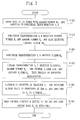
- Fig. 3 is a flow chart illustrating an operation of the circuit 30 shown in Fig. 2. An operation of the circuit 30 is explained with reference to Fig. 3.
- Input data X1 (a plaintext, a ciphertext, a key, etc.) is XORed with a random number R 1 at the XOR 4, thereby obtaining X ⁇ XOR>R 1 , which is inputted to the nonlinear transformation S 1 6 (S101).
- Fig. 2 shows an example of layer formation in the order of the nonlinear transformation S 1 6, the linear transformation L 2 , etc. This is only an example. The order of the layers of nonlinear transformation and linear transformation, and the number of layers depend on the algorithm F and the implementation method thereof.
- An input from above to the XOR 5 is 0.
- An output at the top from the random number generator 3 is the random number R 1 .
- Inputs from the right to the nonlinear transformation S 1 6 are the random number R 1 and the random number R 2 .
- the nonlinear transformation S 1 6 receives the control signal en 1 (S102).
- the control signal en 1 changes to "1" later than the changes of the input signals of X ⁇ XOR>R 1 , R 1 , and R 2 .
- This control is performed by the control circuit 8, the timing generation circuit TG 9, and the timing control circuit TC 10.
- the nonlinear transformation S 1 6 outputs X 1 ⁇ XOR>R 2 (S103).
- the linear transformation L 2 7 receives the input signals of X 1 ⁇ XOR>R 2 , R 2 and a control signal en 2 that changes later than these signals change.
- the linear transformation L 2 7 then outputs X 2 ⁇ XOR>R 2 .
- the processes of nonlinear transformation and linear transformation are repeated in the same manner. (S104).
- a result X 1 ⁇ XOR>R 1 outputted from the last transformation layer S n (or L n ) is selected by the selector 2, and inputted to the XOR 4 again.
- an input from above to the XOR 5 is R j
- an output from the top of the random number generator 3 is R j+1 .
- the XOR 4 thus receives R j ⁇ XOR>R j+1 from the right and outputs X i ⁇ XOR>R j+1 (S105).
- the control circuit 8 inputs "1" to the AND gate 11 after the processes of nonlinear transformation and linear transformation required for the process of the cryptographic algorithm F are completed.
- a result X n ⁇ XOR>R m outputted from the last transformation layer S n (or L n ) is then XORed with R m at the XOR 12, and data X n is thus outputted (S106).
- Fig. 4 is a diagram illustrating a configuration of a simplified circuit 31 where the number of random number is reduced to 1 bit in contrast to the circuit 30 shown in Fig. 2.
- the nonlinear transformation S 1 of the circuit 31, for example, is formed by the elementary device A using a 1-bit random number only mentioned earlier.
- the circuit 31 may minimize the number of random numbers used on the circuit and therefore may be implemented with a smaller area of circuit than that of the circuit 30.
- Fig. 5 is a timing chart illustrating the timing of control signals used in each layer of the circuit 30 of Fig. 2 and the circuit 31 of Fig. 4.
- the control signals need initialization to obtain logic 0 for another arithmetic operation.
- the initialization system may include a method of initialization performed after all operations are done. Another method, like the one shown in Fig. 5, starts sequential initialization from the top layer. According to the method of sequential initialization from the top layer, waiting time before the start of the next operation may be shortened, thereby implementing high speed processing. This method, however, requires a register between a layer to be initialized and the next layer in order to store an output from the layer to be initialized. Hence, circuit costs are increased.
- Fig. 6 is a diagram of the elementary device A 100 of a transistor configuration as a concrete embodiment of the previously described elementary device A.
- the third random number r in the equation of z is the second random number.
- the elementary device A 100 receives x 1 and x 2 , which are data obtained by XORing x i and x j with the random number r, respectively, then applies a predetermined logic operation to x i and x j , then XORs a result thereof with the random number r, and outputs an XOR.
- the output is performed as soon as when all input signals are settled. Consequently, an output signal is not affected by the transient transition of an input signal.
- an output is performed all at once without generating intermediate data between an input and an output. This makes it possible to defend against an attack that tries to identify confidential information by power consumption.
- the elementary device A 100 of Fig. 6 is a 2-input AND type, and outputs the following z as mentioned above:
- Inputs to the nonlinear transformation S 1 , X ⁇ XOR> ⁇ r,r,r,... ,r ⁇ , r and the control signal en, are processed as follows.
- Fig. 7 shows a truth table of the elementary device A 100.
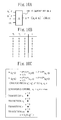
- Fig. 8A to Fig. 8C are diagrams illustrating the roles of the random number r and the control signal en in the elementary device A 100.
- the result becomes the same as that of the 2-input AND gate shown in Fig. 8A.
- Fig. 8B is the truth table of this case.
- the signal transition rates a are different.
- PO is a probability of z being "0”
- P1 is a probability of z being "1”.
- Fig. 9A shows an elementary device A' that does not use the control signal en.
- Fig. 9B shows a truth table of the elementary device A' of Fig. 9A.
- Fig. 9C shows a signal transition rate a of the elementary device A'. According to the truth table of Fig.
- the following is given.
- the elementary device A' when a signal changes in the order of x i , x j , and r, as shown in Fig. 9C, similar bias to that of Fig. 8C occurs in the signal transition rate a during the time when x j changes, for example. Consequently, power consumption may be used to predict an input to the AND gate. If the changing order of x i , x j , and r is different, bias occurs but with a time difference. There is no problem when there is no time difference in the changes of the input signals.
- Fig. 10A to Fig. 10C are diagrams illustrating a process of the elementary device A 100.
- Fig. 10A shows inputs to and an output from the elementary device A 100.
- Fig. 10B shows a truth table of the elementary device A 100.
- Fig. 10C is a diagram illustrating a relationship between the changes of the input signals and an output signal z.
- the signal transition rate ⁇ is 1/2, regardless of the values, 0 or 1, of x i and x j .
- the output z of the elementary device A 100 is always 0 when the control signal en is 0.
- the input/output values are processed as follows. Values to be processed in a conventional process, x i , x j , etc. are XORed with the random number, processed in the operation using the control signal en, and a result may then be outputted. There is an alternative process system that may output an arbitrary value. These systems may be applied to an three- or more input AND operation and three- or more input other operations of such as OR, NOR, NAND, XOR, etc. to form a nonlinear transformation layer or a linear transformation layer.
- Fig. 11 shows an equivalent circuit to one shown in Fig. 6, for example.
- An AND circuit 40 of Fig. 11 performs the process of x i &x j , which means that the operation of the gate is therefore the same as that of one of Fig. 8A. Accordingly, bias will occur in the signal transition rate a, so that an input to the AND gate 40 becomes predictable.
- the "equivalent circuit" of Fig. 11 and the device 20 of Fig. 1 are equivalent.
- the device 20 is a convenient configuration for the explanation of the elementary device A.
- a conventional value of an input/output value is XORed with a random number, and a result is outputted at once by the control signal en.
- it is required to perform the process by a single arithmetic element for outputting the output z at once like the elementary device A 100 of Fig. 6.
- the elementary device A 100 of the first embodiment uses a single arithmetic element to make the signal transition rate a equal. In addition to this, transient transition does not occur in the output z. For this reason, such a condition mentioned above that "it is required that complementary circuits operate with the same timing" is not needed. Therefore, efficient countermeasures may be implemented.
- the elementary device A 100 of Fig. 6 is provided with a single output line only. Therefore, there is no need for considering "load equalization of output lines", which is needed to be considered with the gate pair or the circuit pair.
- the elementary device A receives XOR data X of the n-bit data and the random number R a , performs the predetermined logic operation, and outputs the XOR of a result of the logic operation and the random number r b as the output signal. Therefore, the signal transition rate of the output signal may be made equal. Thus, the bias in power consumption may be eliminated, thereby defending against an attack trying to identify confidential information by power consumption.
- the elementary device A of the first embodiment a single kind of the random number r is used for processing, thereby minimizing the number of kinds of random numbers to be used. Therefore, the area of implementation may be made smaller than that when using multiple kinds of random numbers.
- the elementary device A according to the first embodiment performs processing when the state transition of the input signal is completed, and then output the output signal. Therefore, the signal transition of the output may be made equal.
- the elementary device A outputs the output z by using the control signal en (a command signal) that instructs the elementary device A to output it. Therefore, the signal transition rate may be made equal.
- the elementary device A 100 may serve to defend against an attack trying to identify confidential information by power consumption.
- the elementary device A 100 is the hardware based countermeasures with the transistor circuit configuration. Therefore, higher speed processing is possible with the elementary device A 100 than software based countermeasures.
- the elementary device A 100 uses the single kind of the random number r for processing, thereby serving to minimize the number of the kinds of random numbers to be used. Therefore, the area of implementation may be made smaller than that when using multiple kinds of random numbers.
- the elementary device A 100 outputs the output z by using the control signal en (a command signal) that instructs the elementary device A to output it. Therefore, the signal transition rate may be made equal.
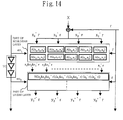
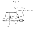
- FIG. 12A A second embodiment is now discussed with reference to Fig. 12A to Fig. 16.
- an LUT 200 (shown in Fig. 15 elaborated later) is described.
- the LUT 200 may implement an equivalent function to that of the elementary device A 100 of the first embodiment shown in Fig. 6 by using a memory element.
- the "S-box” is a conversion table that is used for an operation in which a predetermined output is performed upon receipt of a specific input.
- DES defines eight kinds of tables for 6-bit inputs and 4-bit outputs.
- a conversion table such as this may be implemented by AND-XOR circuits alone.
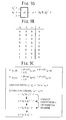
- Fig. 12A is a diagram showing inputs/outputs of a table S1 that is defined by a DES algorithm.
- the table S1 receives 6-bit data ⁇ X 5 , X 4 , X 3 , X 2 , X 1 , X 0 ⁇ , converts the data to 4-bit data ⁇ y 3 , y 2 , y 1 , y 0 ⁇ , and then outputs the 4-bit data.
- Fig. 12B is a diagram showing the content of the table S1.
- a row is determined by ⁇ X 5 , X 0 ⁇ of the input data ⁇ X 5 , X 4 , X 3 , X 2 , X 1 , X 0 ⁇ .
- a column is determined by ⁇ X 4 , X 3 , X 2 , X 1 ⁇ .
- Fig. 12C is a diagram showing an example of an input value and an output value.
- MOSFET Metal Oxide Semiconductor Field Effect Transistor
- FPGA Field Programable Gate Array
- SRAM Static Random Access Memory
- Fig. 15 is a diagram illustrating a configuration that implements an equivalent function to the elementary device A 100 of Fig. 6 using the LUT 200 having four inputs and one output.
- the LUT 200 which is equivalent to the elementary device A 100, receives the inputs of x 1 , x 2 , r and en.
- the LUT 200 includes an input portion 250, a plurality of SRAMs 260 etc. (storage portions), and a plurality of pass-transistors 280 etc.
- the SRAM has a function to store a value to implement a logic function.
- a data stream 270 (logic data) is formed by data stored in the SRAMs.
- the pass-transistor has a function to switch right and left connections.
- a pass-transistor is placed at each branch in a tree structure.
- the pass-transistors are placed each at thirty branches, branch 201 to branch 230.
- An input signal line switches ON/OFF of the pass-transistor provided at each branch.
- the pass-transistor as a switching function opens when receiving "0".
- the control signal en is not needed. In this case, transistors corresponding to the signals perform switching at the same time.
- the LUT 200 according to the second embodiment may serve to defend against an attack trying to identify confidential information by power consumption.
- the LUT 200 according to the second embodiment may serve to minimize the number of kinds of random numbers to be used based on the process using one kind of the random number r. This may make the area of implementation smaller than that when multiple kinds of random numbers are used.
- the LUT 200 performs simultaneous switching by the plurality of transistors. This may make the signal transition rate equal without a transient process occurring during an input to an output.
- the LUT 200 outputs the output z by using the control signal en (a command signal) that instructs the LUT to output it. This may make the signal transition rate equal.
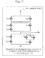
- Fig. 17 to Fig. 24 show a series of elementary devices that are also designed to defend against an attack trying to identify confidential information by power consumption, like the elementary device A 100, the LUT 200, etc.
- Fig. 17 is a diagram illustrating an elementary device A 300 according to a third embodiment.
- the elementary device A 300 modifies the elementary device A 100 of Fig 6 by removing the transistor 101 and the transistor 107 that receive the control signal en. That is, the elementary device A 300 receives input signals x 1 , x 2 and r.
- the control signal en does not exist.
- the elementary device A 300 is designed assuming that the input signals x 1 , x 2 and r are inputted to the respective transistors with the same timing. In other words, the input signals are inputted at the same time, so that corresponding transistors perform switching at the same time. This is done because the control signal en is not needed.
- the elementary device A 300 of the third embodiment does not require the input of the control signal en, and therefore may be implemented in a simplified form.
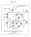
- Fig. 18 is a diagram illustrating an elementary device A 400 according to the third embodiment.
- the elementary device A 400 is a 2-input OR type whereas the elementary device A 100 of Fig. 6 is a 2-input AND type.
- the elementary device A 400 receives input signals x 1 , x 2 and r.
- the output z is outputted at once by switching by the respective transistors based on the control signal en. This makes it possible to defend against an attack trying to identify confidential information by power consumption like the elementary device A 100.
- Fig. 19 is a diagram illustrating an elementary device A 500 according to the third embodiment.
- the elementary device A 500 is a 2-input NAND type whereas the elementary device A 100 of Fig. 6 is a 2-input AND type.
- the input signals are x 1 , x 2 , r and en.
- the output z is outputted as soon as possible by switching by the respective transistors based on the control signal en. This makes it possible to defend against an attack trying to identify confidential information by power consumption like the elementary device A 100.
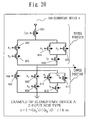
- Fig. 20 is a diagram illustrating an elementary device A 600 according to the third embodiment.
- the elementary device A 600 is a 2-input NOR type whereas the elementary device A 100 of Fig. 6 is a 2-input AND type.
- the input signals are x 1 , x 2 , r and en.
- the inputs x 1 and x 2 are:
- Fig. 21 is a diagram illustrating an elementary device B 700 according to the third embodiment.
- the elementary device B 700 is a 2-input XOR type whereas the elementary device A 100 of Fig. 6 is a 2-input AND type.
- the input signals are x 1 , x 2 , r and en.
- inputs x 1 and x 2 are:
- Fig. 22 is a diagram illustrating an elementary device A 800 according to the third embodiment.
- the elementary device A 800 is a 3-input AND type whereas the elementary device A 100 of Fig. 6 is a 2-input AND type.
- the input signals are x 1 , x 2 , x 3 , r and en.
- Fig. 23 is a graph showing time variation of power consumption when an attack is made to identify confidential information from power consumption.
- Fig. 23 shows the time variation of power consumption sampled prior to countermeasures being taken for a circuit formed by AND circuits and XOR circuits without using the elementary device A or the elementary device B. As the figure shows, peaks appear in consumed energy when an AND operation and an XOR operation are executed. The presence of the peak may identify confidential information.
- Fig. 24 is a comparative example to Fig. 23 showing a result of countermeasures being taken with the elementary device A or the elementary device B. No such peak as those in Fig. 23 appears. The absence of the peak may prevent confidential information from being identified.
Landscapes
- Engineering & Computer Science (AREA)
- Computer Security & Cryptography (AREA)
- Computer Networks & Wireless Communication (AREA)
- Signal Processing (AREA)
- Storage Device Security (AREA)
- Logic Circuits (AREA)
Abstract
Description
- The present invention relates to an electronic device that forms a semiconductor for implementing cryptographic algorithms. For example, this invention relates to an electronic device and a data processing method that defend against an attack trying to identify confidential information processed within a device based on the power consumption of the device.
- Conventional countermeasures for protecting confidential information on semiconductor devices are divided roughly into two types: software based countermeasures using a specific semiconductor device, which is typified by Central Processing Unit (CPU), and hardware based countermeasures on the semiconductor device itself.
- The software based countermeasures of the former case are implemented by a device formed by both a CPU and a memory in itself, which is typified by an IC card.
JP2000066585 JP2002540654T - The hardware based countermeasures of the latter case are implemented by a design method for implementing algorithms by a semiconductor device. For example,
JP2003526134T JP2002311826 JP2003526134T - In principle, with those conventional gate-pair based countermeasures, confidential information may be deciphered for the following reason.
- The security of the gate pair is based on a fully complementary operation performed by the AND gate and the INV-AND gate. To meet this condition, it is required that the pair of the AND gate and the INV-AND gate operate with the same timing and also that loads connected to the gates are the same. This is because a tiny gap in operation timing will also cause a time difference in power consumption to be measured, so that power resulting from the gates will be measured with a phase difference. If the gate loads of the AND gate and the INV-AND gate of a gate pair are different from each other, then the power consumptions of the two gates measured immediately after their operations are also different. This easily shows which gate operated. This does not provide a complementary operation. A gate added to provide a complimentary operation (which will be referred to hereinafter as a dummy gate) is a redundant gate in terms of logical implementation, and therefore an output from the gate is not used. Therefore, the dummy gate tends to have load smaller than that of a necessary gate. In order to have load equalization, a pair may be formed by whole circuits instead of gates, which is exemplified by the countermeasures described in
JP2002311826
Patent Document 1:JP2000066585
Patent Document 2:JP2002540654T
Patent Document 3:JP2003526134T
Patent Document 4:JP2002311826 - It is an object of the present invention to solve the problem of time difference and the problem of load balancing by providing a semiconductor device configured to perform a complementary operation in principle with a single output node.
- An electronic device according to this invention may be characterized in that the electronic device may receive as an input signal a result of an XOR operation of predetermined data with a first random number, perform a predetermined logic operation based on the input signal received, perform an XOR operation of a result of the logic operation with a second random number, and output a result of the XOR operation of the result of the logic operation with the second random number as an output signal.
- An electronic device according to this invention may be characterized in that the electronic device may receive XOR data indicating data obtained by XORing data of n bits (n≧1) with a first random number of n bits, the first random number of n bits, and a second random number of 1 bit as input signals, perform an XOR operation of the XOR data with the first random number to obtain the data of n bits, perform a predetermined logic operation using each bit of the data of n bits obtained, perform an XOR operation of a result of the logic operation with the second random number, and output as an output signal a result of the XOR operation of the result of the logic operation with the second random number.
- The first random number may be characterized by being an n-bit random number, each bit having a same value, and the second random number may be characterized by being the same value as that of the each bit of the first random number.
- The electronic device may be characterized by being independent of the state transitions of the input signals, and outputting the output signal without performing transitional processes.
- The electronic device may be characterized by further receiving a command signal that instructs the electronic device to output the output signal, and outputting the output signal upon receipt of the command signal.
- The predetermined logic operation may be characterized by being selected from among a logical multiply (AND) operation, a negative AND (NAND) operation, a logical add (OR) operation, a negative OR (NOR) operation, and an exclusive-OR (XOR) operation.
- An electronic device according to this invention may be characterized by being formed by a plurality of transistors. The electronic device may also be characterized by receiving a first random number, a second random number, and n-bit data (n≧1), and outputting a predetermined signal as an output signal. The electronic device may also be characterized by outputting by switching of the plurality of transistors the output signal indicating an equivalent result of a result obtained by processes of an XOR operation of the first random number with the n-bit data upon receipt of the first random number, the second random number, and the n-bit data, a predetermined logic operation using each bit indicating a result of the XOR operation, and an XOR operation of a result of the predetermined logic operation with the second random number.
- The first random number may be characterized by being an n-bit random number, each bit having a same value, and the second random number may be characterized by being a 1-bit random number having the same value as that of the each bit of the first random number.
- The electronic device may be characterized in that the plurality of transistors may perform simultaneous switching.
- The electronic device may be characterized by receiving a command signal that instructs the elementary device to output the output signal, and outputting the output signal upon receipt of the command signal.
- An electronic device according to this invention may be characterized by receiving a first random number, a second random number, and n-bit data (n≧1), and outputting a predetermined signal as an output signal. The electronic device may also be characterized by including a receiving portion that may receive the first random number, the second random number, and the n-bit data; a storing portion that may store logic data formed by 0 and 1; and a plurality of transistors. Each of the plurality of transistors may retrieve, when the receiving portion receives the first random number, the second random number and the n-bit data, by switching from the logic data stored in the storing portion an equivalent result to a result obtained by processes of an XOR operation of the first random number with the n-bit data, then a predetermined logic operation using each bit indicating a result of the XOR operation, and then an XOR operation of a result of the predetermined logic operation with the second random number, and outputting the equivalent result as the output signal.
- The first random number may be characterized by being an n-bit random number, each bit having a same value, and the second random number may be characterized by being a 1-bit random number having the same value as that of the each bit of the first random number.
- The plurality of transistors may be characterized by performing simultaneous switching.
- The receiving portion may be characterized by further receiving a command signal that instructs the electronic device to output the output signal. The electronic device may be characterized by outputting the output signal upon receipt of the command signal.
- A data processing method according to this invention may be characterized by including: receiving as an input signal a result of an XOR operation of predetermined data with a first random number; performing a predetermined logic operation based on the input signal received; performing an XOR operation of a result of the logic operation with a second random number; and outputting as an output signal a result of the XOR operation of the result of the logic operation with the second random number.
- A data processing method according to this invention may be characterized by including: receiving as input signals XOR data indicating data obtained by XORing data of n bits with a first random number of n bits, the first random number of n bits, and a second random number of 1 bit; performing an XOR operation of the XOR data with the first random number to obtain the data of n bits; performing a predetermined logic operation using each bit of the data of n bits obtained; performing an XOR operation of a result of the logic operation with the second random number; and outputting as an output signal a result of the XOR operation of the result of the logic operation with the second random number.
- This invention may be used to defend against an attack trying to identify confidential information by power consumption without having a circuit performing a complementary operation.
- A first embodiment will be discussed with reference to Fig. 1 through Fig. 11. The first embodiment relates to an elementary device A for nonlinear transformation, an elementary device B for linear transformation, and a circuit processing cryptographic algorithms by using the elementary device A and the elementary device B. The XOR of n-bit data A and n-bit data B on a bit-by-bit basis will be referred to hereinafter also as A<XOR>B.
- An arbitrary cryptographic algorithm F is always a combination of a nonlinear transformation Si (0≦i≦p) and a linear transformation Lj (0≦j≦q) to ensure its security. This combination is necessary so as to be equivalently replaced by another combination of an AND (logical multiply) gate and an XOR (exclusive OR) gate when the algorithm is implemented by a digital circuit. Alternatively, the implementation is, of course, possible with any combinations of basic logic gates, such as OR (logic add), NOR (negative OR), NAND (negative AND), etc. All processes performed by those combinations may also be equivalently replaced by the combination of an AND gate and an XOR gate. Given this fact, a discussion will be given, focusing on the AND gate and the XOR gate. Claims, however, are directed to all the basic gates of AND, XOR, OR, NOR, NAND, etc.
- First, a description is given of the elementary device A as a component of the nonlinear transformation Si. A device as a component of a nonlinear transformation will be referred to hereinafter as the elementary device A. The nonlinear transformation Si is assumed to be formed by the elementary device A.
- Fig. 1 is a diagram showing a
device 20 of convenience for illustrating a process of the elementary device A, assuming that the elementary device A receives 2-bit input data (x1, y2). Thedevice 20 of Fig. 1 shows a configuration of convenience to explain the process of the elementary device A. Thedevice 20 is not shown as an embodiment of the elementary device A. A concrete embodiment of the elementary device A will be described later with reference to anelementary device A 100 in Fig. 6. - The
device 20 includes anXOR 22, an ANDgate 23, anXOR 27, and an ANDgate 24. Thedevice 20 receives x1(x1=xi^r) and x2(x2=x1^r), which are the XOR of (xi,yi) with a random number r, respectively. Thedevice 20 also receives the random number r and a control signal en 26. - An operation of the
device 20 is described. - (1) The
device 20 receives x1(x1=xi^r) and x2(x2=xj^r), which are the XOR of the data (xi,yi) (an example of predetermined data) with the random number r (an example of the first random number). - (2) The
XOR 22 receives (x1,x2) (an example of XOR data) and the random number r and performs an XOR operation. Specifically, "xi^r^r" and "xj^r^r" are executed. TheXOR 22 then outputs Xi and Xj. - (3) The AND
gate 23 receives Xi and xj, and outputs "Xi&Xj" (an output point 25). - (4) The
XOR 27 receives the random number r (an example of a second random number) and "xi&xj", and outputs "xi&xj^r". - (5) The AND
gate 24 receives "xi&xj^r" and the control signal en 26, and outputs "z=xi&xj^r" when the control signal en 26 is "1". This is however only an example. The operation of the elementary device A may be implemented by replacing the ANDgate 24 by an OR gate if the control signal en is "0" effective.
If the control signal en is a kind of signal that determines effectiveness at a "leading edge" or a "trailing edge", then the ANDgate 24 may be replaced by a flip-flop, so that the operation of the elementary device A is implemented by an operation of a system receiving the output of theXOR 27 at the "leading edge" or the "trailing edge" of the control signal en. To make the explanation simple, it is assumed the control signal en is "1" effective, and the operation of the elementary device A is explained with reference to the operation explained with the ANDgate 24. Claims, however, are directed to all systems where signals are effective when "0", "1", "at a leading edge" and "at a trailing edge". This also applies to the elementary device B. - Next, a description is given of a case of n-bit input in contrast with the case of 2-bit input of the
device 20 shown in Fig. 1. For example, n-input AND is implemented by the elementary device A that performs the following processes (1a) through (4a) in each nonlinear process of the nonlinear transformation Si. The elementary device A receives X(x1, X2, ···, xn) of n-bit data, Ra (r1, r2, ···, rn)(an example of the first random number) of an n-bit random number, rb (an example of the second random number) of a 1-bit random number, and the control signal en (an example of a command signal). The elementary device A then outputs
- (1a) The n-bit input X(x1, x2, ... , xn)(an example of XOR data) is XORed with the n-bit random number Ra(r1,r2,.. .,rn)(note: x1, x2, etc. had already been XORed with the random number Ra before being inputted). This is referred to as X'. With the
device 20, x1=xi^r,x2=xj^r. A random number Ra is Ra=(r1,r2)=(r,r). Accordingly, X'=(xi,xj). - (2a) All the bits of X' are ANDed. This is referred to as x". With the
device 20, x"=xi&xj. - (3a) The x" is XORed with the 1-bit random number rb. This is referred to as y. With the
device 20, rb=r, and y=xi&xj^r. - (4a) The y and the control signal en are ANDed and then outputted. This is referred to as z. With the
device 20, z=xi&xj^r as mentioned earlier. Note: z is outputted as soon as possible by setting the control signal en to "1" after all the input signals are settled. - All the processes of (1a) through (4a) are performed by a single arithmetic element. The elementary device A operates the processes, which forms the nonlinear transformation Si. The output z is outputted as soon as possible by setting the control signal en to "1" after all the input signals are settled.
- The elementary device A is characterized as follows. The elementary device A receives data that is obtained by XORing data to be processed by conventional cryptographic algorithms (xi, xj, etc.) with a random number. The elementary device A then XORs a result of a predetermined logic operation of data to be processed by the conventional process with a random number, and outputs an XOR result. The XOR result is outputted after all the input signals are settled. This characteristic makes it possible to defend against an attack trying to identify confidential information processed within the device by the power consumption thereof. Reasons of defence are as follows. The output z is the XOR of the random number r. The probability ratio of "0" and "1" appearing as the random number r is 1/2, so that the signal transition rate a of the output z is 1/2. In addition to this, the output signal z is outputted after the state transitions of all the input signals are completed and processes are performed. The "processes" here is a series of processes including: performing an XOR operation of X (XOR data), the n-bit data, with the random number Ra (the first random number) to obtain n-bit data, performing an AND operation (an example of the predetermined logic operation) using each bit of the n-bit data obtained, and performing an XOR operation of a result of the AND operation (a logic operation) with the random number rb (the second random number). It is thus impossible for an attacker to detect any change in the power of the output z. The same is applied to the elementary device B, which will be discussed later. This characteristic will be further elaborated with reference to Fig. 8 to Fig. 11.
- It is also possible to use one bit for the random number for the purpose of making the configuration of the elementary device A simplified. Specifically,
- (1b) The n-bit input X (x1,x2,···,xn) is XORed with an n-bit string of 1-bit random numbers r. This is referred to as X'. That is,

- (2b) The X' is ANDed for all the bits. This is referred to as x". That is,

- (3b) The x" is XORed with r. This is referred to as y. That is,

- (4b) The y and the control signal en are ANDed, and the AND is to be outputted. This is referred to as z.
- The elementary device B forming the linear transformation Lj is now explained in outline.
A device forming a linear transformation will be referred to hereinafter as the elementary deice B. It is assumed that the linear transformation Lj is formed by the elementary device B. In each linear process of the linear transformation Lj, an n-input XOR is implemented by a device performing the process such as follows, for example. - (1c) The n-bit input X(x1,x2, -,xn) is XORed for all the bits. This is referred to as x'. That is,

- (2c) The x' is XORed with the 1-bit random number r. This is referred to as y. That is,

- (3c) The y and the control signal en are ANDed, and the AND is to be outputted. This is referred to as z.
- The control signal en used as an input to the elementary device A and the elementary device B is made to change considerably later than other input signals to the elementary devices change. Specifically, the elementary device A and the elementary device B each output a result in the form of:
- "(an intermediate value of a cryptographic algorithm or a process result thereof)^ a random number value"
- only when the control signal en is logical "1". In all other cases, 0 is always outputted. The cryptographic algorithm F is formed by using the elementary device A and the elementary device B. Like the case of the "last transformation layer" of Fig. 2 discussed below, a ciphertext or a plaintext may be obtained by XORing a result from the elementary device A or the elementary device B with the same random number used in the previous process.
- A description is now given of a circuit that processes cryptographic algorithms using the elementary device A and the elementary device B with reference to Fig. 2. Fig 2 is a schematic block diagram of a configuration of a circuit 30 that processes the cryptographic algorithm F using the elementary device A and the elementary device B. Application algorithms are not limited because the elementary device A and the elementary device B are countermeasures against the basic operation of cryptographic algorithms of the smallest unit.
- The circuit 30 includes a
selector 2, arandom number generator 3, anXOR 4, anXOR 5, nonlinear transformations S1 6 etc.,linear transformations L 2 7 etc., acontrol circuit 8, a timinggeneration circuit TG 9, a timingcontrol circuit TC 10, an ANDgate 11, anXOR 12, aregister 13, and aregister 14. Thenonlinear transformation S 1 6, thelinear transformation L 2 7, etc. are formed in layers. A nonlinear transformation Si is formed by the elementary device A. A linear transformation Lj is formed by the elementary device B. - Fig. 3 is a flow chart illustrating an operation of the circuit 30 shown in Fig. 2. An operation of the circuit 30 is explained with reference to Fig. 3.
- Input data X1 (a plaintext, a ciphertext, a key, etc.) is XORed with a random number R1 at the
XOR 4, thereby obtaining X<XOR>R1, which is inputted to the nonlinear transformation S1 6 (S101). Fig. 2 shows an example of layer formation in the order of thenonlinear transformation S 1 6, the linear transformation L2, etc. This is only an example. The order of the layers of nonlinear transformation and linear transformation, and the number of layers depend on the algorithm F and the implementation method thereof. An input from above to theXOR 5 is 0. An output at the top from therandom number generator 3 is the random number R1. Inputs from the right to thenonlinear transformation S 1 6 are the random number R1 and the random number R2. From the left thenonlinear transformation S 1 6 receives the control signal en1 (S102). The control signal en1 changes to "1" later than the changes of the input signals of X<XOR>R1, R1, and R2. This control is performed by thecontrol circuit 8, the timinggeneration circuit TG 9, and the timingcontrol circuit TC 10. Thenonlinear transformation S 1 6 outputs X1<XOR>R2 (S103). Likewise, thelinear transformation L 2 7 receives the input signals of X1<XOR>R2, R2 and a control signal en2 that changes later than these signals change. Thelinear transformation L 2 7 then outputs X2<XOR>R2. The processes of nonlinear transformation and linear transformation are repeated in the same manner. (S104). - When the nonlinear transformation and the linear transformation are processed in the same circuit, a result X1<XOR>R1 outputted from the last transformation layer Sn (or Ln) is selected by the
selector 2, and inputted to theXOR 4 again. In this case, an input from above to theXOR 5 is Rj, and an output from the top of therandom number generator 3 is Rj+1. TheXOR 4 thus receives Rj<XOR>Rj+1 from the right and outputs Xi<XOR>Rj+1 (S105). - The
control circuit 8 inputs "1" to the ANDgate 11 after the processes of nonlinear transformation and linear transformation required for the process of the cryptographic algorithm F are completed. A result Xn<XOR>Rm outputted from the last transformation layer Sn (or Ln) is then XORed with Rm at theXOR 12, and data Xn is thus outputted (S106). - Fig. 4 is a diagram illustrating a configuration of a
simplified circuit 31 where the number of random number is reduced to 1 bit in contrast to the circuit 30 shown in Fig. 2. The nonlinear transformation S1 of thecircuit 31, for example, is formed by the elementary device A using a 1-bit random number only mentioned earlier. Thecircuit 31 may minimize the number of random numbers used on the circuit and therefore may be implemented with a smaller area of circuit than that of the circuit 30. - Fig. 5 is a timing chart illustrating the timing of control signals used in each layer of the circuit 30 of Fig. 2 and the
circuit 31 of Fig. 4. When a "start" signal becomes effective to start the process of cryptographic algorithms, the process of the input data X1 is performed and then completed at theselector 2 and theXOR 4. When the process results thereof are fully transmitted to the elementary device A that forms the nonlinear transformation S1, the control signal en (S1) of the first layer S1 changes tologic 1. Then, S1 outputs an arithmetic result, and data is transmitted to the elementary device B that forms L2. When all data is transmitted, the control signal (L2) of L2 changes tologic 1. This operation is repeated in the subsequent layers. The control signal en (S2l-1) of the final layer S2i-1 finally changes tologic 1. - The control signals need initialization to obtain
logic 0 for another arithmetic operation. The initialization system may include a method of initialization performed after all operations are done. Another method, like the one shown in Fig. 5, starts sequential initialization from the top layer. According to the method of sequential initialization from the top layer, waiting time before the start of the next operation may be shortened, thereby implementing high speed processing. This method, however, requires a register between a layer to be initialized and the next layer in order to store an output from the layer to be initialized. Hence, circuit costs are increased. - Fig. 6 is a diagram of the
elementary device A 100 of a transistor configuration as a concrete embodiment of the previously described elementary device A. Theelementary device A 100 of Fig. 6 receives x1(x1=xi^r), x2(x2=xj^r), the random number r, and the control signal en (an example of a command signal), and outputs
where the random numbers r that are XORed with x1 and x2 are the first random number. The third random number r in the equation of z is the second random number. - A configuration of the
elementary device A 100 is explained with reference to Fig. 6. - (1) The
elementary device A 100 is formed by series-connectedupper portion 115 andlower portion 116. An output signal z is outputted between theupper portion 115 and thelower portion 116. - (2) In Fig. 6, a sign "!" denotes an inversion of a signal. A right-pointing arrow "→" added to each transistor forming the
upper portion 115 means that the transistor becomes ON when the signal is "0". A left-pointing arrow "←" added to each transistor forming theupper portion 116 means that the transistor becomes ON when the signal is "1". Theupper portion 115 is therefore an aggregate of transistors that become ON when a signal is "0". Thelower portion 116 is therefore an aggregate of transistors that become ON when a signal is "1". Avoltage applying portion 113 receives voltage corresponding to logic "1". - (3) When voltage corresponding to logic "1" is applied to the
voltage applying portion 113,
- (4) The transistor configuration of the
elementary device A 100 is explained. Theupper portion 115 includes a serial connection of atransistor 101, a parallel circuit oftransistors transistors transistor 106. - (5) The
lower portion 116 is formed by a parallel connection of atransistor 107, series-connectedtransistors transistors transistor 112. Thetransistors earth 114 at one end. - (6) An input signal is now explained. A signal is always inverted before inputted to a transistor.
An input signal x1, inverted, is inputted to thetransistor 102, thetransistor 104,transistor 108, andtransistor 110. - (7) An input signal x2, inverted, is inputted to the
transistor 103, thetransistor 105, thetransistor 109, and thetransistor 111. - (8) An input signal r, inverted, is inputted to the
transistor 106 and thetransistor 112. - (9) An input signal en, inverted, is inputted to the
transistor 101 and thetransistor 107. - The
elementary device A 100, as mentioned earlier, receives x1 and x2, which are data obtained by XORing xi and xj with the random number r, respectively, then applies a predetermined logic operation to xi and xj, then XORs a result thereof with the random number r, and outputs an XOR. The output is performed as soon as when all input signals are settled. Consequently, an output signal is not affected by the transient transition of an input signal. In addition to this, an output is performed all at once without generating intermediate data between an input and an output. This makes it possible to defend against an attack that tries to identify confidential information by power consumption. - The
elementary device A 100 of Fig. 6 is a 2-input AND type, and outputs the following z as mentioned above:
where x1=xj^r, and x2=xj^r.
When the nonlinear transformation S1 of Fig. 4 is formed by theelementary device A 100, the following is given. Inputs to the nonlinear transformation S1, X<XOR>{r,r,r,... ,r}, r and the control signal en, are processed as follows. Theelementary device A 100 processes arbitrary two bits using A(xi^r,xj^r), and then outputs z. That is,
When en=1, then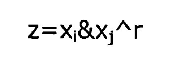
is outputted. - Fig. 7 shows a truth table of the
elementary device A 100. When x1=0, the signal transition rate a(x1=0) of the signal of output z changing "from 0 to 1" or "from 1 to 0" is:
where PO is a probability when z is "0", and P1 is a probability when z is
"1". According to the truth table,
PO=4/8, and
P1=4/8.
P1(x1=0) is a probability of z being "1" under the condition that x1=0. P0(x1=0) is a probability of z being "0" under the condition that x1=0. According to the truth table,

Therefore:
With x1=1, according to the truth table,

when calculated in the same manner.
Therefore,
Therefore, the signal transition rate α is the same when the input x1 (or x2) is 0 as when it is 1. The output z is outputted as soon as by the control signal en when input signals are settled. Consequently, an output signal is not affected by the transient transition of an input signal. In addition to this, output is performed at once without generating intermediate data between an input and an output. Therefore, with the elementary device A, it is not possible to predict confidential information by power consumption. - Fig. 8A to Fig. 8C are diagrams illustrating the roles of the random number r and the control signal en in the
elementary device A 100. When the previously mentioned process of xi&xj in theelementary device A 100 is performed without using the random number r and the control signal en, the result becomes the same as that of the 2-input AND gate shown in Fig. 8A. Fig. 8B is the truth table of this case. According to the truth table of Fig. 8B, the signal transition rate a is:

Thus, the signal transition rates a are different. - A more detailed explanation is given with reference to Fig. 8C. First, when xj=0, a signal transition rate a (xi=0) of the signal of the output z changing "from 0 to 1" or "from 1 to 0" is:

Note: PO is a probability of z being "0", and P1 is a probability of z being "1". According to the truth table of Fig. 8B, P0= 3/4 and P1=1/4.
P1(xj=0) is a probability of z being "1" under the condition of xi=0.
P0(xi=0) is a probability of z being "0" under the condition of xi=0.
According to the truth table,

Therefore:

When xi=0, according to the truth table,
are obtained in the same manner. Therefore,
Consequently, as mentioned above,

Thus, the signal transition rate a is biased. - Thus, with the 2-input AND shown in Fig. 8A, there is a power difference between when an input, xi (or xj), is 0 and when it is 1. Consequently, power consumption may be used to predict an input to the AND gate. This makes it possible to identify confidential information used in the process.
- Next, a description is given of the control signal en with reference to Fig. 9A to Fig. 9C. Fig. 9A shows an elementary device A' that does not use the control signal en. With the elementary device A', when there is a time difference between the changes in the input signals, signal changes independent of random numbers occur in transient transition, which causes bias in the signal transition rate a. This makes it impossible to identify confidential information. Fig. 9B shows a truth table of the elementary device A' of Fig. 9A. Fig. 9C shows a signal transition rate a of the elementary device A'. According to the truth table of Fig. 9B, both the signal transition rate a (xi=0) and the signal transition rate α (xi=1) relating to the output z are 1/2. When there is a time difference between the changes in the input signals, however, the following is given. With the elementary device A', when a signal changes in the order of xi, xj, and r, as shown in Fig. 9C, similar bias to that of Fig. 8C occurs in the signal transition rate a during the time when xj changes, for example. Consequently, power consumption may be used to predict an input to the AND gate. If the changing order of xi, xj, and r is different, bias occurs but with a time difference. There is no problem when there is no time difference in the changes of the input signals.
- Fig. 10A to Fig. 10C are diagrams illustrating a process of the
elementary device A 100.
Fig. 10A shows inputs to and an output from theelementary device A 100.
Fig. 10B shows a truth table of theelementary device A 100.
Fig. 10C is a diagram illustrating a relationship between the changes of the input signals and an output signal z.
In Fig. 10C, according to the truth table of Fig. 10B, the signal transition rate α is 1/2, regardless of the values, 0 or 1, of xi and xj. In addition to this, as shown in Fig. 10C, the output z of theelementary device A 100 is always 0 when the control signal en is 0. Therefore, if the control signal en is made to 1 after changes are made to the signals xi, xj, and r, then transient transition does not occur to the output z, so that transition occurs always with an equal transition rate a. It is impossible therefore to specify confidential information from power consumption - As mentioned above, the input/output values are processed as follows. Values to be processed in a conventional process, xi, xj, etc. are XORed with the random number, processed in the operation using the control signal en, and a result may then be outputted. There is an alternative process system that may output an arbitrary value. These systems may be applied to an three- or more input AND operation and three- or more input other operations of such as OR, NOR, NAND, XOR, etc. to form a nonlinear transformation layer or a linear transformation layer.
- When the elementary device is formed by the previously described method, if the device is simply a combination of conventional basic gates and performs the same operation as that mentioned above, the device does not function as countermeasures. Fig. 11 shows an equivalent circuit to one shown in Fig. 6, for example. An AND
circuit 40 of Fig. 11 performs the process of xi&xj, which means that the operation of the gate is therefore the same as that of one of Fig. 8A. Accordingly, bias will occur in the signal transition rate a, so that an input to the ANDgate 40 becomes predictable. The "equivalent circuit" of Fig. 11 and thedevice 20 of Fig. 1 are equivalent. At theoutput point 25 of thedevice 20, like the ANDgate 40, bias occurs in the signal transition rate αo For this reason, thedevice 20 is a convenient configuration for the explanation of the elementary device A. In order to prevent confidential information from leaking from power consumption, a conventional value of an input/output value is XORed with a random number, and a result is outputted at once by the control signal en. To implement this process, it is required to perform the process by a single arithmetic element for outputting the output z at once like theelementary device A 100 of Fig. 6. - A system that equalizes the signal transition rate a with complementary circuits, such as the gate pair of
JP2003526134T JP2002311826 elementary device A 100 of the first embodiment, however, uses a single arithmetic element to make the signal transition rate a equal. In addition to this, transient transition does not occur in the output z. For this reason, such a condition mentioned above that "it is required that complementary circuits operate with the same timing" is not needed. Therefore, efficient countermeasures may be implemented. In addition to this, theelementary device A 100 of Fig. 6 is provided with a single output line only. Therefore, there is no need for considering "load equalization of output lines", which is needed to be considered with the gate pair or the circuit pair. - The elementary device A according to the first embodiment receives XOR data X of the n-bit data and the random number Ra, performs the predetermined logic operation, and outputs the XOR of a result of the logic operation and the random number rb as the output signal. Therefore, the signal transition rate of the output signal may be made equal. Thus, the bias in power consumption may be eliminated, thereby defending against an attack trying to identify confidential information by power consumption.
- According to the elementary device A of the first embodiment, a single kind of the random number r is used for processing, thereby minimizing the number of kinds of random numbers to be used. Therefore, the area of implementation may be made smaller than that when using multiple kinds of random numbers.
- The elementary device A according to the first embodiment performs processing when the state transition of the input signal is completed, and then output the output signal. Therefore, the signal transition of the output may be made equal.
- The elementary device A according to the first embodiment outputs the output z by using the control signal en (a command signal) that instructs the elementary device A to output it. Therefore, the signal transition rate may be made equal.
- The
elementary device A 100 according to the first embodiment may serve to defend against an attack trying to identify confidential information by power consumption. In addition to this, theelementary device A 100 is the hardware based countermeasures with the transistor circuit configuration. Therefore, higher speed processing is possible with theelementary device A 100 than software based countermeasures. - The
elementary device A 100 according to the first embodiment uses the single kind of the random number r for processing, thereby serving to minimize the number of the kinds of random numbers to be used. Therefore, the area of implementation may be made smaller than that when using multiple kinds of random numbers. - The
elementary device A 100 according to the first embodiment outputs the output z by using the control signal en (a command signal) that instructs the elementary device A to output it. Therefore, the signal transition rate may be made equal. - A second embodiment is now discussed with reference to Fig. 12A to Fig. 16. In the second embodiment, an LUT 200 (shown in Fig. 15 elaborated later) is described. The
LUT 200 may implement an equivalent function to that of theelementary device A 100 of the first embodiment shown in Fig. 6 by using a memory element. - First, a configuration method of DES S-boxes as an example of a nonlinear layer is described. Then, an application of the
LUT 200 to the S-boxes will be discussed. - The "S-box" is a conversion table that is used for an operation in which a predetermined output is performed upon receipt of a specific input. DES defines eight kinds of tables for 6-bit inputs and 4-bit outputs. A conversion table such as this may be implemented by AND-XOR circuits alone.
- Fig. 12A is a diagram showing inputs/outputs of a table S1 that is defined by a DES algorithm. As shown in Fig. 12A, the table S1 receives 6-bit data {X5, X4, X3, X2, X1, X0}, converts the data to 4-bit data {y3, y2, y1, y0}, and then outputs the 4-bit data.
- Fig. 12B is a diagram showing the content of the table S1. Referring to the table S1 of Fig. 12B, a row is determined by {X5, X0} of the input data {X5, X4, X3, X2, X1, X0}. A column is determined by {X4, X3, X2, X1}.
- Fig. 12C is a diagram showing an example of an input value and an output value. When


Therefore, the second row is determined of the table S1. Then,
Therefore, the 14th column is determined of the table S1. Therefore, {011011} is converted to "5" (0101) in the second row at the 14th column. - Equivalent transformations are possible from "14, 4, 13, ... 0, 7" of the first row of the table S1 in Fig. 12B to the equations of y0' to y3' shown in Fig. 13. Likewise, the second and subsequent rows may also be transformed. The equations of Fig. 13, like the case of the
circuit 31 of Fig. 4, may be formed by a single nonlinear layer and a single linear layer like the one shown in Fig. 14. Referring to Fig. 14, like the case of Fig. 4, input data is XORed with the random number r before being inputted to a nonlinear layer. Then, an AND operation is performed in the first layer of the nonlinear layer, and then an XOR operation is performed in the second layer of the linear layer. - The previously explained countermeasures are assumed to be formed by MOSFET (Metal Oxide Semiconductor Field Effect Transistor) like the
elementary device A 100 of Fig. 6. Alternatively, however, it is also possible that a MOSFET level design is not used in a circuit for cryptographic algorithms. For example, a rewritable semiconductor device typified by FPGA (Field Programable Gate Array) may also be used. In this case, the designer is allowed to alter the internal state of a memory element (referred to hereinafter as LUT) that is formed by SRAM (Static Random Access Memory) mounted on a chip in advance, the internal state of a storage element typified by a flip-flop, and the wiring thereof only. Fig. 15 shows an embodiment using such a device. - Fig. 15 is a diagram illustrating a configuration that implements an equivalent function to the
elementary device A 100 of Fig. 6 using theLUT 200 having four inputs and one output. - The
LUT 200, which is equivalent to theelementary device A 100, receives the inputs of x1, x2, r and en. The output z is:
- The
LUT 200 includes aninput portion 250, a plurality ofSRAMs 260 etc. (storage portions), and a plurality of pass-transistors 280 etc. The SRAM has a function to store a value to implement a logic function. A data stream 270 (logic data) is formed by data stored in the SRAMs. The pass-transistor has a function to switch right and left connections. - The configuration of the
LUT 200 shown in Fig. 15 is explained. A pass-transistor is placed at each branch in a tree structure. The pass-transistors are placed each at thirty branches,branch 201 tobranch 230. An input signal line switches ON/OFF of the pass-transistor provided at each branch. The pass-transistor as a switching function opens when receiving "0". -
- (1) Next, a configuration of the
LUT 200 is explained. With theLUT 200, the output z branches into two branches of thebranch 201 and abranch 202. Thebranch 202 branches into two branches of abranch 205 and abranch 206. Thebranch 205 branches into two branches of abranch 211 and abranch 212. Thebranch 206 branches into two branches of abranch 213 and abranch 214. Thebranch 211 branches into two branches of abranch 223 and abranch 224. Thebranch 212 branches into two branches of abranch 225 and abranch 226. Thebranch 213 branches into two branches of abranch 227 and abranch 228. Thebranch 214 branches into two branches of abranch 229 and thebranch 230. Each of "thebranch 223, thebranch 224, ..., and thebranch 230" is connected to a SRAM. - (2) The
branch 201 branches in a similar manner to thebranch 202. Thebranch 201 branches into two branches of abranch 203 and abranch 204. Thebranch 203 branches into two branches of abranch 207 and abranch 208. Thebranch 204 branches into two branches of abranch 209 and abranch 210. Thebranch 207 branches into two branches of abranch 215 and abranch 216. Thebranch 208 branches into two branches of abranch 217 and abranch 218. Thebranch 209 branches into two branches of abranch 219 and abranch 220. Thebranch 210 branches into two branches of abranch 221 and abranch 222. Each of "thebranch 215, thebranch 216, ..., and thebranch 222" is connected to a SRAM. In Fig. 15, the SRAMs connected to thebranch 216, thebranch 218, and thebranch 220 each store "1". The other SRAMs each store "0". - (3) An input signal is explained. An inverted signal of the input signal x2 is inputted to a pass-transistor placed at the
branch 201. The input signal x2 is inputted to a pass-transistor placed at thebranch 202. An inverted signal of the input signal x1 is inputted to pass-transistors placed at thebranch 203 and thebranch 205. The input signal x1 is inputted to pass-transistors placed at thebranch 204 and thebranch 206. An inverted signal of the input signal r is inputted to pass-transistors placed at thebranch 207, thebranch 209, thebranch 211, and thebranch 213. The input signal r is inputted to pass-transistors placed at thebranch 208, thebranch 210, thebranch 212, and thebranch 214. An inverted signal of the input signal en is inputted to pass-transistors placed at thebranch 215, thebranch 217, thebranch 219, thebranch 221, thebranch 223, thebranch 225, thebranch 227, and thebranch 229. The input signal en is inputted to pass-transistors placed at thebranch 216, thebranch 218, thebranch 220, thebranch 222, thebranch 224, thebranch 226, thebranch 228, and thebranch 230. - If the control signal en is "0" effective, then the process of "&en" in the previously mentioned z=((x1^r)&(x2^r)^r)&en changes to "|en" (OR with the control signal en). An equivalent function to the elementary device A may thus be implemented by LUT in the same way.
- If the input signals x1, x2 and r are inputted at the same time, then the control signal en is not needed. In this case, transistors corresponding to the signals perform switching at the same time.
- If the same process system is also applied to OR, NOR, NAND, XOR, etc. that receive two inputs, then an attack trying to identify confidential information by power consumption may be defended.
- With an elementary device having three or more inputs, in general, the size of the LUT is fixed in many cases. Therefore, as shown in Fig. 16, it is practical to use elementary devices having two inputs in combination. In this case, two different control signals are needed. The reason is given. As shown in Fig. 16, there is a time difference in signal change between an input to an
LUT 292, which is outputted from anLUT 291, and the other inputs to theLUT 292, which are not outputted from theLUT 291. Therefore, if a control signal is shared, then the randomness of the random number does not work on the previously mentioned grounds (the transient transition of an input signal). - The
LUT 200 according to the second embodiment may serve to defend against an attack trying to identify confidential information by power consumption. - The
LUT 200 according to the second embodiment may serve to minimize the number of kinds of random numbers to be used based on the process using one kind of the random number r. This may make the area of implementation smaller than that when multiple kinds of random numbers are used. - The
LUT 200 according to the second embodiment performs simultaneous switching by the plurality of transistors. This may make the signal transition rate equal without a transient process occurring during an input to an output. - The
LUT 200 according to the second embodiment outputs the output z by using the control signal en (a command signal) that instructs the LUT to output it. This may make the signal transition rate equal. - A description is given of elementary devices other than the
elementary device A 100 of Fig. 6 and theLUT 200 of Fig. 15 with reference to Fig. 17 to Fig. 22. Fig. 17 to Fig. 24 show a series of elementary devices that are also designed to defend against an attack trying to identify confidential information by power consumption, like theelementary device A 100, theLUT 200, etc. - Fig. 17 is a diagram illustrating an
elementary device A 300 according to a third embodiment. Theelementary device A 300 modifies theelementary device A 100 of Fig 6 by removing thetransistor 101 and thetransistor 107 that receive the control signal en. That is, theelementary device A 300 receives input signals x1, x2 and r. The output z is:
The control signal en does not exist. Theelementary device A 300 is designed assuming that the input signals x1, x2 and r are inputted to the respective transistors with the same timing. In other words, the input signals are inputted at the same time, so that corresponding transistors perform switching at the same time. This is done because the control signal en is not needed. - The
elementary device A 300 of the third embodiment does not require the input of the control signal en, and therefore may be implemented in a simplified form. - Fig. 18 is a diagram illustrating an
elementary device A 400 according to the third embodiment. Theelementary device A 400 is a 2-input OR type whereas theelementary device A 100 of Fig. 6 is a 2-input AND type. Theelementary device A 400 receives input signals x1, x2 and r. The output z is:
The inputs x1 and x2 are:
x1=xi^r and x2=xj^r , respectively, like the case of theelementary device A 100. Therefore, an input/output is XORed with a random number. In addition to this, the output z is outputted at once by switching by the respective transistors based on the control signal en. This makes it possible to defend against an attack trying to identify confidential information by power consumption like theelementary device A 100. - (1) A configuration of the
elementary device A 400 is explained. Theelementary device A 400 is formed by series-connectedupper portion 415 andlower portion 416. The output signal z is outputted between theupper portion 415 and thelower portion 416. - (2) With reference to Fig. 18, a sign "!", a right-pointing arrow "→", and a left-pointing arrow "←" denote the same as those of Fig. 6. The same applies to those of Fig. 19 to Fig. 22 discussed later. Voltage corresponding to logic "1" is applied to a
voltage applying portion 413. - (3) When the voltage corresponding to logic "1" is applied to the
voltage applying portion 413,
- (4) The
upper portion 415 is formed by series-connectedtransistor 401 and apartial circuit 417. Thetransistor 401 is connected to thevoltage applying portion 413 at one end and thepartial circuit 417 at the other end. Thepartial circuit 417 is formed by a parallel connection of series-connectedtransistors transistors transistor 406. - (5) The
lower portion 416 is formed in the same manner as that of thelower portion 116 of theelementary device A 100 of Fig. 6. Specifically, the arrangement of atransistor 407 to atransistor 412 is the same as that of thetransistor 107 to thetransistor 112. Thetransistor 412 of thelower portion 416, however, receives the input signal r, which is not inverted, whereas thetransistor 112 of thelower portion 116 receives the inverted signal of the input signal r. - (6) Next, the input signal is explained. An inverted signal of the input signal x1 is inputted to the
transistor 402, thetransistor 404, atransistor 408, and atransistor 410. - (7) An inverted signal of the input signal x2 is inputted to the
transistor 403, thetransistor 405, atransistor 409, and atransistor 411. (7) The input signal r is inputted to thetransistor 406 and thetransistor 412. - (8) An inverted signal of the input signal en is inputted to the
transistor 401 and thetransistor 407. - Fig. 19 is a diagram illustrating an
elementary device A 500 according to the third embodiment. Theelementary device A 500 is a 2-input NAND type whereas theelementary device A 100 of Fig. 6 is a 2-input AND type. The input signals are x1, x2, r and en. The output z is:
Inputs x1 and x2 are:
respectively. Therefore, an input/output is XORed with a random number. In addition to this, the output z is outputted as soon as possible by switching by the respective transistors based on the control signal en. This makes it possible to defend against an attack trying to identify confidential information by power consumption like theelementary device A 100. -
- (1) The configuration of the
elementary device A 500 is the same as that of theelementary device A 500 of Fig. 18 as shown in Fig. 19, but the signal inversion of input signals to the respective transistors is different. - (2) Input signals are explained. The input signal x1 is inputted to a
transistor 502, atransistor 504, atransistor 508, and atransistor 510. - (3) The input signal x2 is inputted to a
transistor 503, atransistor 505, atransistor 509, and atransistor 511. - (4) The input signal r is inputted to a
transistor 506, and atransistor 512. - (5) An inverted signal of the input signal en is inputted to a transistor 301 and a transistor 307.
- Fig. 20 is a diagram illustrating an
elementary device A 600 according to the third embodiment. Theelementary device A 600 is a 2-input NOR type whereas theelementary device A 100 of Fig. 6 is a 2-input AND type. The input signals are x1, x2, r and en. The output z is:
Like the case of theelementary device A 100, the inputs x1 and x2 are: - x1=xi^r and x2=xj^r,
- (1) The configuration of the
elementary device A 600 is the same as that of theelementary device A 300 of Fig. 18 as shown in Fig. 20, but the signal conversion of signals to be inputted to the respective transistors is different. - (2) Input signals are explained. The input signal x1 is inputted to a
transistor 602, atransistor 604, atransistor 608, and atransistor 610. - (3) The input signal x2 is inputted to a
transistor 603, atransistor 605, and atransistor 609. An inverted signal of the input signal x2 is inputted to atransistor 611. - (4) An inverted signal of the input signal r is inputted to a
transistor 606, and atransistor 612. - (5) An inverted signal of the input signal en is inputted to a
transistor 601 and atransistor 607. - Fig. 21 is a diagram illustrating an
elementary device B 700 according to the third embodiment. Theelementary device B 700 is a 2-input XOR type whereas theelementary device A 100 of Fig. 6 is a 2-input AND type. The input signals are x1, x2, r and en. The output z is:
Like the case of theelementary device A 100, inputs x1 and x2 are: - x1=xl^r and x2=xj^r,
- (1) The
elementary device B 700 is formed by series-connectedupper portion 721 andlower portion 722. The output signal z is outputted between theupper portion 721 and thelower portion 722. - (2) Voltage corresponding to logic "1" is applied to a
voltage applying portion 719. - (3) When voltage corresponding to logic "1" is applied to the
voltage applying portion 719,
- (4) The
upper portion 721 is formed by atransistor 701 and apartial circuit 727 connected in series. Thetransistor 701 is connected to thevoltage applying portion 719 at one end and thepartial circuit 727 at the other end. - (5) A configuration of the
partial circuit 727 is explained. Thepartial circuit 727 is formed by a parallel connection of series-connectedtransistor 702 andparallel circuit 723 and series-connectedparallel circuit 724 andtransistor 709. More specifically, theparallel circuit 723 is formed by a parallel connection of series-connectedtransistors transistors
Theparallel circuit 724 is formed by atransistor 705 and atransistor 706. - (6) A configuration of the
lower portion 722 is now explained. Thelower portion 722 is formed by a parallel connection of atransistor 710, series-connectedparallel circuit 725 andtransistor 715, and series-connectedparallel circuit 726 andtransistor 718. More specifically, theparallel circuit 725, like theparallel circuit 723, is formed by a parallel connection of series-connectedtransistors transistors parallel circuit 726 is formed by atransistor 716 and atransistor 717. - (7) Next, input signals to the respective transistors are explained. The input signal x1 is inputted to the
transistor 703, thetransistor 707, thetransistor 711, and thetransistor 716. An inverted signal of the input signal x1 is inputted to thetransistor 705, and thetransistor 713. The input signal x2 is inputted to thetransistor 704, thetransistor 708, thetransistor 712, and thetransistor 717. An inverted signal of the input signal x2 is inputted to thetransistor 706, and thetransistor 714. The input signal r is inputted to thetransistor 709 and thetransistor 718. An inverted signal of the input signal r is inputted to thetransistor 702 and thetransistor 715. An inverted signal of the input signal en is inputted to thetransistor 701 and thetransistor 710. - Fig. 22 is a diagram illustrating an
elementary device A 800 according to the third embodiment. Theelementary device A 800 is a 3-input AND type whereas theelementary device A 100 of Fig. 6 is a 2-input AND type. The input signals are x1, x2, x3, r and en. The output z is:
Like the case of theelementary device A 100, inputs x1, x2 and x3 are:
respectively. Therefore, an input/output is XORed with a random number. In addition to this, z is outputted as soon as possible by switching performed by the respective transistors based on the control signal en. This makes it possible to defend against an attack trying to identify confidential information from power consumption like theelementary device A 100. -
- (1) The
elementary device A 800 is formed by anupper portion 819 and alower portion 820 connected in series. The output signal z is outputted between theupper portion 819 and thelower portion 820. - (2) Voltage corresponding to logic "1" is applied to a
voltage applying portion 817. - (3) When voltage corresponding to logic "1" is applied to the
voltage applying portion 817,:
- (4) The
upper portion 819 is formed by a series connection of atransistor 801, a partial circuit of atransistor 802, atransistor 803, and a transistor 804, and a parallel circuit of series-connectedtransistors transistor 808. - (5) The
lower portion 820 is formed by a parallel circuit of atransistor 809, series-connectedtransistors transistors transistor 816. - (6) Input signals to the respective transistors are now explained. With the
elementary device A 800, all the input signals x1, x2, x3, r and en are inverted and then inputted to the respective transistors. An inverted signal of the input signal x1 is inputted to thetransistor 802, thetransistor 805, thetransistor 810, and thetransistor 813. An inverted signal of the input signal x2 is inputted to thetransistor 803, thetransistor 806, thetransistor 811 and thetransistor 814. An inverted signal of the input signal x3 is inputted to the transistor 804, thetransistor 807, thetransistor 812, and thetransistor 815. An inverted signal of the input signal r is inputted to thetransistor 808 and thetransistor 816. An inverted signal of the input signal en is inputted to thetransistor 801 and thetransistor 809. - Fig. 23 is a graph showing time variation of power consumption when an attack is made to identify confidential information from power consumption. Fig. 23 shows the time variation of power consumption sampled prior to countermeasures being taken for a circuit formed by AND circuits and XOR circuits without using the elementary device A or the elementary device B. As the figure shows, peaks appear in consumed energy when an AND operation and an XOR operation are executed. The presence of the peak may identify confidential information.
- Fig. 24 is a comparative example to Fig. 23 showing a result of countermeasures being taken with the elementary device A or the elementary device B. No such peak as those in Fig. 23 appears. The absence of the peak may prevent confidential information from being identified.
-
- [Fig. 1] It is a diagram illustrating a
device 20, which is a convenient example provided for explaining the process of an elementary device A according to a first embodiment. - [Fig. 2] It is a block diagram illustrating a schematic configuration of a circuit 30 according to the first embodiment.
- [Fig. 3] It is a flow chart illustrating an operation of the circuit 30 according to the first embodiment.
- [Fig. 4] It is a diagram illustrating a configuration of a
circuit 31 according to the first embodiment. - [Fig. 5] It is a timing chart of control signals used in the layers of the circuit 30 and the
circuit 31 according to the first embodiment. - [Fig. 6] It is a diagram of an
elementary device A 100 according to the first embodiment. - [Fig. 7] It shows a truth table of the
elementary device A 100 according to the first embodiment. - [Fig. 8A] It shows a 2-input AND gate.
- [Fig. 8B] It shows a truth table of the 2-input AND gate.
- [Fig. 8C] It is a diagram illustrating a signal transition rate of the 2-input AND gate.
- [Fig. 9A] It shows a 2-input AND gate.
- [Fig. 9B] It shows a truth table of the 2-input AND gate.
- [Fig. 9C] It is a diagram illustrating transient transition in relation to the signal transition rate of the 2-input AND gate.
- [Fig. 10A] It shows inputs to and an output from the
elementary device A 100 according to the first embodiment. - [Fig. 10B] It shows a truth table of the
elementary device A 100 according to the first embodiment. - [Fig. 10C] It is a diagram illustrating a change of an input signal in relation to an output signal z of the
elementary device A 100 according to the first embodiment. - [Fig. 11] It is a diagram showing a circuit that is logically equivalent to the
elementary device A 100. - [Fig. 12A] It is a diagram showing inputs/outputs of a table S1 that is defined by a DES algorithm.
- [Fig. 12B] It is a diagram showing a content of the table S1.
- [Fig. 12C] It is a diagram showing an example of an input value and an output value.
- [Fig. 13] It shows equations obtained by processing data of the first row of the table S1 by equivalent transformation.
- [Fig. 14] It is a diagram illustrating a circuit configuration for executing the equations shown in Fig. 13.
- [Fig. 15] It is a diagram of a
LUT 200 according to a second embodiment. - [Fig. 16] It is a diagram of a circuit formed by a combination of 2-input elementary devices according to the second embodiment.
- [Fig. 17] It is a diagram of an
elementary device A 300 according to a third embodiment. - [Fig. 18] It is a diagram of an
elementary device A 400 according to the third embodiment. - [Fig. 19] It is a diagram of an
elementary device A 500 according to the third embodiment. - [Fig. 20] It is a diagram of an
elementary device A 600 according to the third embodiment. - [Fig. 21] It is a diagram of an
elementary device B 700 according to the third embodiment. - [Fig. 22] It is a diagram of an
elementary device A 800 according to the third embodiment. - [Fig. 23] It is a graph of time-varying power consumption before countermeasures are taken against an attack trying to identify confidential information by power consumption.
- [Fig. 24] It is a graph of time-varying power consumption after countermeasures are taken against an attack trying to identify confidential information by power consumption.
- 1 input data X, 2 selector, 3 random number generator, 4,5 exclusive OR, 6 nonlinear transformation S1, 7 linear transformation L2, 8 control circuit, 9 timing generating circuit TG, 10 timing control circuit TC, 11 AND gate, 12 exclusive OR, 13,14 register, 20 device, 21,22 XOR, 23,24 AND gate, 25 output point, 26 control signal en, 27 XOR, 30 circuit, 31 circuit, 40 AND gate, 100 elementary device A, 101-112 transistor, 113 voltage applying portion, 114 earth, 115 upper portion, 116 lower portion, 200 LUT, 201-230 branch, 250 input portion, 260 SRAM, 270 data stream, 280 pass-transistor, 291,292 LUT, 300 elementary device A, 400 elementary device A, 401-412 transistor, 413 voltage applying portion, 414 earth, 415 upper portion, 416 lower portion, 417 partial circuit, 500 elementary device A, 501-512 transistor, 600 elementary device A, 601-612 transistor, 700 elementary device B, 701-718 transistor, 719 voltage applying portion, 720 earth, 721 upper portion, 722 lower portion, 723 parallel circuit, 724,725,726 parallel circuit, 727 partial circuit, 800 elementary device A, 801-816 transistor, 817 voltage applying portion, 818 earth, 819 upper portion, 820 lower portion.
Elementary Device A (X) is:

Elementary Device B (X) is:

When the input X has been XORed with a random number component, e.g., an output from A(X), for example, then the process of (2c) is omitted if X is an odd number bit stream.
Claims (16)
- An electronic device, wherein the electronic device receives as an input signal a result of an XOR operation of predetermined data with a first random number, performs a predetermined logic operation based on the input signal received, performs an XOR operation of a result of the logic operation with a second random number, and outputs a result of the XOR operation of the result of the logic operation with the second random number as an output signal.
- An electronic device, wherein the electronic device receives XOR data indicating data obtained by XORing data of n bits (n≧1) with a first random number of n bits, the first random number of n bits, and a second random number of 1 bit as input signals, performs an XOR operation of the XOR data with the first random number to obtain the data of n bits, performs a predetermined logic operation using each bit of the data of n bits obtained, performs an XOR operation of a result of the logic operation with the second random number, and outputs as an output signal a result of the XOR operation of the result of the logic operation with the second random number.
- The electronic device of claim 2, wherein the first random number is a n-bit random number, each bit having a same value, and
wherein the second random number is the same value as that of the each bit of the first random number. - The electronic device of claim 2, wherein the electronic device performs processes when state transitions of the input signals are completed, and outputs the output signal.
- The electronic device of claim 2, wherein the electronic device further receives a command signal that instructs the electronic device to output the output signal, and outputs the output signal upon receipt of the command signal.
- The electronic device of claim 2, wherein the predetermined logic operation is selected from among a logical multiply (AND) operation, a negative AND (NAND) operation, a logical add (OR) operation, a negative OR (NOR) operation, and an exclusive-OR (XOR) operation.
- An electronic device formed by a plurality of transistors, the electronic device receiving a first random number, a second random number, and n-bit data (n≧1), and outputting a predetermined signal as an output signal, wherein the electronic device outputs by switching of the plurality of transistors the output signal indicating an equivalent result of a result obtained by processes of an XOR operation of the first random number with the n-bit data upon receipt of the first random number, the second random number, and the n-bit data, a predetermined logic operation using each bit indicating a result of the XOR operation, and an XOR operation of a result of the predetermined logic operation with the second random number.
- The electronic device of claim 7, wherein the first random number is an n-bit random number, each bit having a same value, and
wherein the second random number is a 1-bit random number having the same value as that of the each bit of the first random number. - The electronic device of claim 7, wherein the plurality of transistors performs simultaneous switching.
- The electronic device of claim 7, wherein the electronic device receives a command signal that instructs the electronic device to output the output signal, and outputs the output signal upon receipt of the command signal.
- An electronic device that receives a first random number, a second random number, and n-bit data (n≧1), and outputs a predetermined signal as an output signal, the electronic device comprising:a receiving portion that receives the first random number, the second random number, and the n-bit data;a storing portion that stores logic data formed by 0 and 1; anda plurality of transistors, each transistor retrieving, when the receiving portion receives the first random number, the second random number and the n-bit data, by switching from the logic data stored in the storing portion an equivalent result to a result obtained by an XOR operation of the first random number with the n-bit data, then a predetermined logic operation using each bit indicating a result of the XOR operation, and then an XOR operation of a result of the predetermined logic operation with the second random number, and outputting the equivalent result as the output signal.
- The electronic device of claim 11, wherein the first random number is a n-bit random number, each bit having a same value, and
wherein the second random number is a 1-bit random number having the same value as that of the each bit of the first random number. - The electronic device of claim 11, wherein the plurality of transistors performs simultaneous switching.
- The electronic device of claim 11, wherein the receiving portion further receives a command signal that instructs the electronic device to output the output signal, and
wherein the electronic device outputs the output signal upon receipt of the command signal. - A data processing method comprising:receiving as an input signal a result of an XOR operation of predetermined data with a first random number,performing a predetermined logic operation based on the input signal received,performing an XOR operation of a result of the logic operation with a second random number, andoutputting as an output signal a result of the XOR operation of the result of the logic operation with the second random number.
- A data processing method comprising:receiving as input signals XOR data indicating data obtained by XORing data of n bits with a first random number of n bits, the first random number of n bits, and a second random number of 1 bit;performing an XOR operation of the XOR data with the first random number to obtain the data of n bits;performing a predetermined logic operation using each bit of the data of n bits obtained;performing an XOR operation of a result of the logic operation with the second random number, andoutputting as an output signal a result of the XOR operation of the result of the logic operation with the second random number.
Applications Claiming Priority (1)
| Application Number | Priority Date | Filing Date | Title |
|---|---|---|---|
| PCT/JP2004/009633 WO2006006199A1 (en) | 2004-07-07 | 2004-07-07 | Electronic element and data processing method |
Publications (3)
| Publication Number | Publication Date |
|---|---|
| EP1764762A1 true EP1764762A1 (en) | 2007-03-21 |
| EP1764762A4 EP1764762A4 (en) | 2009-11-18 |
| EP1764762B1 EP1764762B1 (en) | 2019-05-15 |
Family
ID=35783565
Family Applications (1)
| Application Number | Title | Priority Date | Filing Date |
|---|---|---|---|
| EP04747102.4A Expired - Lifetime EP1764762B1 (en) | 2004-07-07 | 2004-07-07 | Electronic element and data processing method |
Country Status (6)
| Country | Link |
|---|---|
| US (1) | US8577942B2 (en) |
| EP (1) | EP1764762B1 (en) |
| JP (1) | JP4589327B2 (en) |
| CN (1) | CN1957384B (en) |
| TW (1) | TWI276337B (en) |
| WO (1) | WO2006006199A1 (en) |
Families Citing this family (10)
| Publication number | Priority date | Publication date | Assignee | Title |
|---|---|---|---|---|
| FR2954868A1 (en) * | 2009-12-24 | 2011-07-01 | St Microelectronics Rousset | METHOD AND CONTESSING DEVICE FOR PROTECTING DATA CIRCULATING IN AN ELECTRONIC COMPONENT |
| JP5322977B2 (en) * | 2010-03-04 | 2013-10-23 | 株式会社エヌ・ティ・ティ・データ | Power consumption confusion type logic circuit and information storage medium |
| WO2012014291A1 (en) | 2010-07-28 | 2012-02-02 | 学校法人立命館 | Tamper-resistant memory integrated circuit and encryption circuit using same |
| JP2012150661A (en) * | 2011-01-19 | 2012-08-09 | Toshiba Corp | Processor operation inspection system and its inspection method |
| US10905305B2 (en) * | 2011-05-20 | 2021-02-02 | Ecolab Usa Inc. | Automated cleaning method and apparatus |
| CN104333362B (en) * | 2014-09-16 | 2017-07-04 | 哈尔滨工业大学(威海) | A kind of same or XOR double track precharge logical unit |
| CN108092760A (en) * | 2016-11-22 | 2018-05-29 | 北京同方微电子有限公司 | A kind of co-processor device of block cipher and non-linear transformation method |
| TWI631544B (en) * | 2017-03-03 | 2018-08-01 | 友達光電股份有限公司 | Display panel and driving method |
| CN110414276B (en) * | 2018-04-27 | 2021-05-18 | 联华电子股份有限公司 | Encryption method for electronic component |
| CN109359470B (en) * | 2018-08-14 | 2020-09-01 | 阿里巴巴集团控股有限公司 | Multi-party security calculation method and device and electronic equipment |
Family Cites Families (18)
| Publication number | Priority date | Publication date | Assignee | Title |
|---|---|---|---|---|
| US5808486A (en) * | 1997-04-28 | 1998-09-15 | Ag Communication Systems Corporation | Glitch free clock enable circuit |
| EP1088295B1 (en) | 1998-06-03 | 2007-08-15 | Cryptography Research Inc. | Balanced cryptographic computational method and apparatus for leak minimization in smartcards and other cryptosystems |
| IL139935A (en) | 1998-06-03 | 2005-06-19 | Cryptography Res Inc | Des and other cryptographic processes with leak minimization for smartcards and other cryptosystems |
| JP3600454B2 (en) * | 1998-08-20 | 2004-12-15 | 株式会社東芝 | Encryption / decryption device, encryption / decryption method, and program storage medium therefor |
| DE19850721A1 (en) | 1998-11-03 | 2000-05-18 | Koninkl Philips Electronics Nv | Disk with concealment of power consumption |
| FR2789776B1 (en) | 1999-02-17 | 2001-04-06 | Gemplus Card Int | COUNTER-MEASUREMENT METHOD IN AN ELECTRONIC COMPONENT USING A SECRET KEY CRYPTOGRAPHY ALGORITHM |
| FR2790890B1 (en) * | 1999-03-08 | 2001-04-27 | Gemplus Card Int | COUNTER-MEASUREMENT METHOD IN AN ELECTRONIC COMPONENT USING A SECRET KEY CRYPTOGRAPHY ALGORITHM |
| JP2000305453A (en) * | 1999-04-21 | 2000-11-02 | Nec Corp | Ciphering device, deciphering device, and ciphering and deciphering device |
| JP2001016196A (en) * | 1999-04-28 | 2001-01-19 | Fuji Soft Abc Inc | Encryption / decryption method using multiple affine keys, authentication method, and devices using the same |
| JP3844116B2 (en) | 2001-04-16 | 2006-11-08 | 株式会社ルネサステクノロジ | Encryption / decryption device and IC card |
| JP4596686B2 (en) | 2001-06-13 | 2010-12-08 | 富士通株式会社 | Secure encryption against DPA |
| KR100446317B1 (en) * | 2001-12-24 | 2004-09-01 | 주식회사 하이닉스반도체 | System for protecting data of code ROM in code ROM test |
| DE10201449C1 (en) * | 2002-01-16 | 2003-08-14 | Infineon Technologies Ag | Arithmetic unit, method for performing an operation with an encrypted operand, carry select adder and cryptography processor |
| EP1351148A3 (en) | 2002-04-04 | 2008-05-07 | Texas Instruments Incorporated | Power profiling system and method for correlating runtime information |
| US7403620B2 (en) | 2002-07-02 | 2008-07-22 | Stmicroelectronics S.A. | Cyphering/decyphering performed by an integrated circuit |
| KR101061906B1 (en) * | 2004-02-19 | 2011-09-02 | 삼성전자주식회사 | Basic Computing Device and Method Safe for Power Analysis Attack |
| KR100594265B1 (en) * | 2004-03-16 | 2006-06-30 | 삼성전자주식회사 | Data encryption processing apparatus, AES encryption system and AES encryption method to which the masking method is applied. |
| JP4271077B2 (en) * | 2004-04-30 | 2009-06-03 | 株式会社東芝 | Mask logic circuit and encryption device |
-
2004
- 2004-07-07 JP JP2006527641A patent/JP4589327B2/en not_active Expired - Lifetime
- 2004-07-07 EP EP04747102.4A patent/EP1764762B1/en not_active Expired - Lifetime
- 2004-07-07 WO PCT/JP2004/009633 patent/WO2006006199A1/en not_active Ceased
- 2004-07-07 US US11/629,358 patent/US8577942B2/en not_active Expired - Fee Related
- 2004-07-07 CN CN2004800431276A patent/CN1957384B/en not_active Expired - Fee Related
- 2004-08-04 TW TW093123315A patent/TWI276337B/en not_active IP Right Cessation
Also Published As
| Publication number | Publication date |
|---|---|
| EP1764762B1 (en) | 2019-05-15 |
| US8577942B2 (en) | 2013-11-05 |
| CN1957384B (en) | 2011-04-06 |
| TWI276337B (en) | 2007-03-11 |
| EP1764762A4 (en) | 2009-11-18 |
| JP4589327B2 (en) | 2010-12-01 |
| US20080021940A1 (en) | 2008-01-24 |
| CN1957384A (en) | 2007-05-02 |
| WO2006006199A1 (en) | 2006-01-19 |
| JPWO2006006199A1 (en) | 2008-04-24 |
| TW200603591A (en) | 2006-01-16 |
Similar Documents
| Publication | Publication Date | Title |
|---|---|---|
| US20050169463A1 (en) | Hardware cryptographic engine and hardware cryptographic method using an efficient S-BOX implementation | |
| KR100585119B1 (en) | Encryption apparatus, encryption method and recording medium thereof | |
| EP1764762B1 (en) | Electronic element and data processing method | |
| US20030161467A1 (en) | Compact crypto-engine for random number and stream cipher generation | |
| KR100574965B1 (en) | Finite Field Multiplier | |
| CN104301096B (en) | AES takes turns operation method and circuit | |
| Rais et al. | Efficient hardware realization of advanced encryption standard algorithm using Virtex-5 FPGA | |
| Purohit et al. | FPGA implementation of the AES algorithm with lightweight LFSR-based approach and optimized key expansion | |
| Kaur et al. | Efficient implementation of AES algorithm in FPGA device | |
| Alshammari | Cryptanalysis of a bilateral-diffusion image encryption algorithm based on dynamical compound chaos | |
| Lac et al. | Thwarting fault attacks using the internal redundancy countermeasure (IRC) | |
| Masoumi et al. | Design and evaluation of basic standard encryption algorithm modules using nanosized complementary metal–oxide–semiconductor–molecular circuits | |
| US7613295B2 (en) | Cryptographic device and associated methods | |
| US7464130B2 (en) | Logic circuit and method for performing AES MixColumn transform | |
| Nadjia et al. | Efficient implementation of AES S-box in LUT-6 FPGAs | |
| KR100861841B1 (en) | Electronic device and data processing method | |
| Gupta et al. | Advanced Encryption Standard Algorithm with Optimal S-box and Automated Key Generation | |
| Jansen et al. | Cascade jump controlled sequence generator and Pomaranch stream cipher | |
| Harshitha et al. | High performance advanced encryption standard system using secure double rate registers | |
| Saqib et al. | A compact and efficient FPGA implementation of the DES algorithm | |
| Lakshmi et al. | Enhance Speed Low Area FPGA Design Using S-Box GF and Pipeline Approach on Logic for AES. | |
| JP2018155922A (en) | Feedback shift register circuit and operation method of feedback shift register | |
| Sarkar et al. | Efficient Implementation of “Large” Stream Cipher Systems | |
| EP1575209B1 (en) | Cryptographic device and associated method | |
| Tijare et al. | Verilog implementation of AES 256 algorithm |
Legal Events
| Date | Code | Title | Description |
|---|---|---|---|
| PUAI | Public reference made under article 153(3) epc to a published international application that has entered the european phase |
Free format text: ORIGINAL CODE: 0009012 |
|
| 17P | Request for examination filed |
Effective date: 20061212 |
|
| AK | Designated contracting states |
Kind code of ref document: A1 Designated state(s): DE FR GB |
|
| DAX | Request for extension of the european patent (deleted) | ||
| RBV | Designated contracting states (corrected) |
Designated state(s): DE FR GB |
|
| A4 | Supplementary search report drawn up and despatched |
Effective date: 20091016 |
|
| RIC1 | Information provided on ipc code assigned before grant |
Ipc: H04L 9/06 20060101AFI20091012BHEP |
|
| 17Q | First examination report despatched |
Effective date: 20100126 |
|
| GRAP | Despatch of communication of intention to grant a patent |
Free format text: ORIGINAL CODE: EPIDOSNIGR1 |
|
| INTG | Intention to grant announced |
Effective date: 20180920 |
|
| GRAJ | Information related to disapproval of communication of intention to grant by the applicant or resumption of examination proceedings by the epo deleted |
Free format text: ORIGINAL CODE: EPIDOSDIGR1 |
|
| GRAS | Grant fee paid |
Free format text: ORIGINAL CODE: EPIDOSNIGR3 |
|
| GRAP | Despatch of communication of intention to grant a patent |
Free format text: ORIGINAL CODE: EPIDOSNIGR1 |
|
| INTC | Intention to grant announced (deleted) | ||
| INTG | Intention to grant announced |
Effective date: 20190205 |
|
| GRAA | (expected) grant |
Free format text: ORIGINAL CODE: 0009210 |
|
| AK | Designated contracting states |
Kind code of ref document: B1 Designated state(s): DE FR GB |
|
| REG | Reference to a national code |
Ref country code: GB Ref legal event code: FG4D |
|
| REG | Reference to a national code |
Ref country code: DE Ref legal event code: R096 Ref document number: 602004053972 Country of ref document: DE |
|
| REG | Reference to a national code |
Ref country code: DE Ref legal event code: R097 Ref document number: 602004053972 Country of ref document: DE |
|
| PLBE | No opposition filed within time limit |
Free format text: ORIGINAL CODE: 0009261 |
|
| STAA | Information on the status of an ep patent application or granted ep patent |
Free format text: STATUS: NO OPPOSITION FILED WITHIN TIME LIMIT |
|
| 26N | No opposition filed |
Effective date: 20200218 |
|
| PGFP | Annual fee paid to national office [announced via postgrant information from national office to epo] |
Ref country code: FR Payment date: 20200612 Year of fee payment: 17 |
|
| PGFP | Annual fee paid to national office [announced via postgrant information from national office to epo] |
Ref country code: GB Payment date: 20200624 Year of fee payment: 17 |
|
| PGFP | Annual fee paid to national office [announced via postgrant information from national office to epo] |
Ref country code: DE Payment date: 20200624 Year of fee payment: 17 |
|
| REG | Reference to a national code |
Ref country code: DE Ref legal event code: R119 Ref document number: 602004053972 Country of ref document: DE |
|
| GBPC | Gb: european patent ceased through non-payment of renewal fee |
Effective date: 20210707 |
|
| PG25 | Lapsed in a contracting state [announced via postgrant information from national office to epo] |
Ref country code: GB Free format text: LAPSE BECAUSE OF NON-PAYMENT OF DUE FEES Effective date: 20210707 Ref country code: DE Free format text: LAPSE BECAUSE OF NON-PAYMENT OF DUE FEES Effective date: 20220201 |
|
| PG25 | Lapsed in a contracting state [announced via postgrant information from national office to epo] |
Ref country code: FR Free format text: LAPSE BECAUSE OF NON-PAYMENT OF DUE FEES Effective date: 20210731 |