EP1758261A1 - A system for wirelessly transmitting and receiving inductively coupled data - Google Patents
A system for wirelessly transmitting and receiving inductively coupled data Download PDFInfo
- Publication number
- EP1758261A1 EP1758261A1 EP05107693A EP05107693A EP1758261A1 EP 1758261 A1 EP1758261 A1 EP 1758261A1 EP 05107693 A EP05107693 A EP 05107693A EP 05107693 A EP05107693 A EP 05107693A EP 1758261 A1 EP1758261 A1 EP 1758261A1
- Authority
- EP
- European Patent Office
- Prior art keywords
- terminals
- antenna circuit
- transmit
- inductive antenna
- series connection
- Prior art date
- Legal status (The legal status is an assumption and is not a legal conclusion. Google has not performed a legal analysis and makes no representation as to the accuracy of the status listed.)
- Granted
Links
Images

Classifications
-
- H—ELECTRICITY
- H04—ELECTRIC COMMUNICATION TECHNIQUE
- H04B—TRANSMISSION
- H04B5/00—Near-field transmission systems, e.g. inductive or capacitive transmission systems
- H04B5/20—Near-field transmission systems, e.g. inductive or capacitive transmission systems characterised by the transmission technique; characterised by the transmission medium
- H04B5/24—Inductive coupling
-
- H—ELECTRICITY
- H04—ELECTRIC COMMUNICATION TECHNIQUE
- H04R—LOUDSPEAKERS, MICROPHONES, GRAMOPHONE PICK-UPS OR LIKE ACOUSTIC ELECTROMECHANICAL TRANSDUCERS; ELECTRIC HEARING AIDS; PUBLIC ADDRESS SYSTEMS
- H04R25/00—Electric hearing aids
- H04R25/55—Electric hearing aids using an external connection, either wireless or wired
- H04R25/554—Electric hearing aids using an external connection, either wireless or wired using a wireless connection, e.g. between microphone and amplifier or using Tcoils
-
- H—ELECTRICITY
- H04—ELECTRIC COMMUNICATION TECHNIQUE
- H04B—TRANSMISSION
- H04B5/00—Near-field transmission systems, e.g. inductive or capacitive transmission systems
- H04B5/20—Near-field transmission systems, e.g. inductive or capacitive transmission systems characterised by the transmission technique; characterised by the transmission medium
- H04B5/22—Capacitive coupling
-
- H—ELECTRICITY
- H04—ELECTRIC COMMUNICATION TECHNIQUE
- H04B—TRANSMISSION
- H04B5/00—Near-field transmission systems, e.g. inductive or capacitive transmission systems
- H04B5/20—Near-field transmission systems, e.g. inductive or capacitive transmission systems characterised by the transmission technique; characterised by the transmission medium
- H04B5/24—Inductive coupling
- H04B5/26—Inductive coupling using coils
-
- H—ELECTRICITY
- H04—ELECTRIC COMMUNICATION TECHNIQUE
- H04B—TRANSMISSION
- H04B5/00—Near-field transmission systems, e.g. inductive or capacitive transmission systems
- H04B5/20—Near-field transmission systems, e.g. inductive or capacitive transmission systems characterised by the transmission technique; characterised by the transmission medium
- H04B5/24—Inductive coupling
- H04B5/26—Inductive coupling using coils
- H04B5/263—Multiple coils at either side
-
- H—ELECTRICITY
- H04—ELECTRIC COMMUNICATION TECHNIQUE
- H04B—TRANSMISSION
- H04B5/00—Near-field transmission systems, e.g. inductive or capacitive transmission systems
- H04B5/40—Near-field transmission systems, e.g. inductive or capacitive transmission systems characterised by components specially adapted for near-field transmission
- H04B5/48—Transceivers
Definitions
- This invention relates to a system for wireless communication between for example a remote controller and a hearing aid such as a behind-the-ear (BTE), an in-the-ear (ITE), an in-the-canal (ITC) or a completely-in-canal (CIC), or an implanted hearing aid.
- BTE behind-the-ear
- ITE in-the-ear
- ITC in-the-canal
- CIC completely-in-canal
- Transmit/receive switching means in hearing aids are used for providing switching between transmit and receive modes in hearing aids for wireless communication.
- This American patent application describes a system wherein an inductive coil operating as an antenna is switched between an equivalent series resonant circuit reducing inductive load in transmit mode and an equivalent parallel resonant circuit increasing inductive load in the receive mode.
- the system further utilises a transmit/receive-switch to establish a voltage protection during the transmit mode of a low noise amplifier (LNA) used for amplifying received data during the receive mode.
- LNA low noise amplifier
- An object of the present invention is to provide a system for providing wireless communication with an improved noise rejection.
- It is a further object of the present invention to provide a hearing aid comprising a system for wireless communication between a hearing aid and a remote controller as well as binaurally between a set of hearing aids.
- a particular advantage of the present invention is the provision of a simple protection of a low noise amplifier amplifying the received communication.
- Another advantage is the provision of transmit/receive switching without loss of performance.
- a system for communicating wirelessly comprising an inductive antenna circuit adapted to transmit and receive inductively coupled signals and having a first and second set of terminals, a driving means connected to said first set of terminals and adapted to drive said inductive antenna circuit during a transmit mode, an amplifier means connected to said second set of terminals and adapted to detect and amplify an incoming differential signal during a receiving mode.
- the system according to the first aspect achieves a common mode rejection of signals electrically coupled to the two antenna terminals.
- the amplifier means coupled as a differential amplifier ensures a significantly improved noise reduction scheme.
- the system according to the first aspect of the present invention further may comprise a current sensing means interconnecting said second set of terminals with a non-inverting input and an inverting input of said amplifier means.
- the current sensing means may comprise a low input impedance buffer having current to voltage conversion capabilities.
- the low input impedance buffer may convert a sensed current to a voltage for the inverting and non-inverting input of the amplifier means.
- the low impedance buffer according to the first aspect of the present invention may comprise a common base coupled transistor.
- the impedance buffer effectively may convert the current generated in the inductive antenna circuit to a voltage to be amplified by the amplifier means.
- the driving means may comprise a first power output presenting a square wave to a first terminal of said first set of terminals and a second power output presenting an inverted square wave to a second terminal of said first set of terminals.
- the inductive antenna circuit advantageously is presented with a square wave alternating between a positive and negative maximum, which enables a differential voltage signal to be transmitted as well as received and differentially amplified by the amplifier means.
- the inductive antenna circuit according to the first aspect of the present invention may comprise a series connection of tuning capacitors on either side of a transmit/receive inductor between said first and second set of terminals. Hence the first and second set of terminals are connected together and therefore no switching between components is required when changing from transmit to receive mode.
- the inductive antenna circuit may comprise a series connection of transmit/receive inductors on either side of a tuning capacitor between said first and second set of terminals.
- This series connection provides a well defined zero point between the first and second set of terminals, and provides, as the above mentioned series connection, an inductive antenna solution which does not require switching between components when changing from transmit to receive mode.
- the inductive antenna circuit according to the first aspect of the present invention may alternatively comprise a first series connection of tuning capacitors on either side of a transmit inductor between said first set of terminals, or a first series connection of transmit inductors on either side of a tuning capacitor between said first set of terminals.
- the inductive antenna circuit may further comprise a second series connection of tuning capacitors on either side of a receive inductor between said second set of terminals, or a second series connection of receive inductors on either side of a tuning capacitor between said second set of terminals.
- the inductive antenna circuit according to the first aspect of the present invention may further comprise a magnetic coupling core.
- the magnetic coupling core advantageously increases the magnetic flux permeability and therefore the transmit inductor and the receive inductor are capable of being reduced in size. This obviously is particularly advantageous for implementation of the system according to the first aspect in a hearing aid.
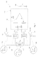
- FIG. 1 shows a system for communicating wirelessly, which is designated in entirety by reference numeral 100.
- the system 100 comprises a set of drivers 102, 104 operating 180° out of phase in transmit mode, shown in graphical representations 106, 108, respectively, so as to establish a square wave transmit signal across a transmit/receive antenna 110, which alternates between a positive maximum and negative minimum, shown in graphical representation 109.
- the transmit/receive antenna In transmit mode the transmit/receive antenna is driven as a full bridge class D transmitter. That is, enveloping the transmit data in pulse width of the square wave transmit signal. In an alternative embodiment the transmit/receive antenna is driven as a half bridge class D.
- the square wave transmit signal may be coded in accordance with any protocol known to a person skilled in the art including any proprietary protocols.
- the system 100 further comprises a low noise amplifier 112 receiving the received signal across a first 114 and second 116 input port.
- the low noise amplifier 112 comprises a differentially coupled operational amplifier 118 amplifying the voltage difference between the first 114 and second 116 input ports and providing an amplified difference signal on output port 120.
- the term "amplified” should be construed as an amplification range from unity to 1000, such as 10 or 100, which amplification obviously is controlled by the value of resistances R1 and R2. It should be understood that this difference amplifier circuit may be implemented in any configurations known to a person skilled in the art.
- the system 100 further comprises current sensing amplifiers 122, 124 interconnecting the end terminals of the transmit/receive antenna 110 and the input ports 114, 116 of the low noise amplifier 120.
- the current sensing amplifiers 122, 124 in the first embodiment of the present invention comprises a low input impedance buffer, such as a common base transistor configuration, for transforming current input signals from the transmit/receive antenna 110 to output voltage signals, which are forwarded to the input ports 114, 116.
- the low input impedance implementation of the current sensing amplifiers 122, 124 further ensures that the resonance frequency of the transmit/receive antenna 110 is not significantly disturbed by the complex imaginary part of the input impedance.
- FIG 2 shows an inductive antenna circuit 110 according to first embodiment of the present invention, which comprises a series connection of tuning capacitors 202, 204 on either side of a transmit/receive inductor 206 between end terminals 208, 210.
- the end terminal 208 is connected to driver 102 and current sensing amplifier 122
- end terminal 210 is connected to driver 104 and current sensing amplifier 124.
- the inductor may be an air coil or a wounded on a ferrite material core.
- FIG 3 shows an inductive antenna circuit 110 according to second embodiment of the present invention, which comprises a series connection of transmit/receive inductors 302, 304 on either side of a tuning capacitor 306 between end terminals 308, 310.
- the end terminal 308 is connected to driver 102 and current sensing amplifier 122
- end terminal 310 is connected to driver 104 and current sensing amplifier 124.
- the two inductors may be air coils or both inductors wound on a single or two separate ferrite material cores.
- FIG 4 shows an inductive antenna circuit 110 according to a third embodiment of the present invention, which comprises a first series connection 402 of tuning capacitors 404, 406 on either side of a transmit inductor 408 between end terminals 410, 412.
- the end terminals 410, 412 are connected to drivers 102 and 104.
- the inductive antenna circuit 110 further comprises a second series connection 414 of tuning capacitors 416, 418 on either side of a receive inductor 420 between end terminals 422, 424.
- the end terminals 422, 424 are connected to current sensing amplifiers 122 and 124.
- the inductive antenna circuit 110 further comprises a magnetic core 426 for supporting the windings of the transmit inductor 408 and the receive inductor 420.
- FIG. 5 shows an inductive antenna circuit 110 according to a fourth embodiment of the present invention, which comprises a first series connection 502 of transmit inductors 504, 506 on either side of a tuning capacitor 508 between end terminals 510, 512.
- the end terminals 510, 512 are connected to drivers 102 and 104.
- the inductive antenna circuit 110 further comprises a second series connection 514 of receive inductors 516, 518 on either side of a tuning capacitor 520 between end terminals 522, 524.
- the end terminals 522, 524 are connected to current sensing amplifiers 122 and 124.
- the inductive antenna circuit 110 further comprises a magnetic core 526 for supporting the windings of the transmit inductors 504, 506 and the receive inductors 516, 518.
Landscapes
- Engineering & Computer Science (AREA)
- Computer Networks & Wireless Communication (AREA)
- Signal Processing (AREA)
- Health & Medical Sciences (AREA)
- General Health & Medical Sciences (AREA)
- Neurosurgery (AREA)
- Otolaryngology (AREA)
- Physics & Mathematics (AREA)
- Acoustics & Sound (AREA)
- Near-Field Transmission Systems (AREA)
- Radar Systems Or Details Thereof (AREA)
- Measuring Pulse, Heart Rate, Blood Pressure Or Blood Flow (AREA)
Abstract
Description
- This invention relates to a system for wireless communication between for example a remote controller and a hearing aid such as a behind-the-ear (BTE), an in-the-ear (ITE), an in-the-canal (ITC) or a completely-in-canal (CIC), or an implanted hearing aid.
- Transmit/receive switching means in hearing aids, such as disclosed in
American patent application no.: US 2005/111682 , are used for providing switching between transmit and receive modes in hearing aids for wireless communication. This American patent application describes a system wherein an inductive coil operating as an antenna is switched between an equivalent series resonant circuit reducing inductive load in transmit mode and an equivalent parallel resonant circuit increasing inductive load in the receive mode. The system further utilises a transmit/receive-switch to establish a voltage protection during the transmit mode of a low noise amplifier (LNA) used for amplifying received data during the receive mode. - Despite the advances achieved within the hearing aid technology by the above described transmit-receive switching means there still is a need for providing improvements of the noise rejection during receive mode, improvements of the voltage protective elements, and provide means for switching between transmit and receive mode without changing the antenna matching.
- An object of the present invention is to provide a system for providing wireless communication with an improved noise rejection.
- It is a further object of the present invention to provide a hearing aid comprising a system for wireless communication between a hearing aid and a remote controller as well as binaurally between a set of hearing aids.
- A particular advantage of the present invention is the provision of a simple protection of a low noise amplifier amplifying the received communication.
- Another advantage is the provision of transmit/receive switching without loss of performance.
- The above objects and advantages together with numerous other objects, advantages and features, which will become evident from below detailed description, are obtained according to a first aspect of the present invention by a system for communicating wirelessly and comprising an inductive antenna circuit adapted to transmit and receive inductively coupled signals and having a first and second set of terminals, a driving means connected to said first set of terminals and adapted to drive said inductive antenna circuit during a transmit mode, an amplifier means connected to said second set of terminals and adapted to detect and amplify an incoming differential signal during a receiving mode.
- The system according to the first aspect achieves a common mode rejection of signals electrically coupled to the two antenna terminals. Hence the amplifier means coupled as a differential amplifier ensures a significantly improved noise reduction scheme.
- The system according to the first aspect of the present invention further may comprise a current sensing means interconnecting said second set of terminals with a non-inverting input and an inverting input of said amplifier means. The current sensing means may comprise a low input impedance buffer having current to voltage conversion capabilities. The low input impedance buffer may convert a sensed current to a voltage for the inverting and non-inverting input of the amplifier means. Hence the problems inheritably associated with prior art switching between a transmitting and receiving mode are avoided, namely problems relating to the amplifier means being exposed to damaging high voltages induced by the inductive antenna circuit during the transmit mode and disturbance of the resonance frequency of the inductive antenna circuit by stray and blocking capacitances or any other protective elements.
- The low impedance buffer according to the first aspect of the present invention may comprise a common base coupled transistor. Thus the impedance buffer effectively may convert the current generated in the inductive antenna circuit to a voltage to be amplified by the amplifier means.
- The driving means according to the first aspect of the present invention may comprise a first power output presenting a square wave to a first terminal of said first set of terminals and a second power output presenting an inverted square wave to a second terminal of said first set of terminals. Hence the inductive antenna circuit advantageously is presented with a square wave alternating between a positive and negative maximum, which enables a differential voltage signal to be transmitted as well as received and differentially amplified by the amplifier means.
- The inductive antenna circuit according to the first aspect of the present invention may comprise a series connection of tuning capacitors on either side of a transmit/receive inductor between said first and second set of terminals. Hence the first and second set of terminals are connected together and therefore no switching between components is required when changing from transmit to receive mode.
- Additionally, or alternatively, the inductive antenna circuit may comprise a series connection of transmit/receive inductors on either side of a tuning capacitor between said first and second set of terminals. This series connection provides a well defined zero point between the first and second set of terminals, and provides, as the above mentioned series connection, an inductive antenna solution which does not require switching between components when changing from transmit to receive mode.
- The inductive antenna circuit according to the first aspect of the present invention may alternatively comprise a first series connection of tuning capacitors on either side of a transmit inductor between said first set of terminals, or a first series connection of transmit inductors on either side of a tuning capacitor between said first set of terminals. The inductive antenna circuit may further comprise a second series connection of tuning capacitors on either side of a receive inductor between said second set of terminals, or a second series connection of receive inductors on either side of a tuning capacitor between said second set of terminals.
- The inductive antenna circuit according to the first aspect of the present invention may further comprise a magnetic coupling core. The magnetic coupling core advantageously increases the magnetic flux permeability and therefore the transmit inductor and the receive inductor are capable of being reduced in size. This obviously is particularly advantageous for implementation of the system according to the first aspect in a hearing aid.
- The above, as well as additional objects, features and advantages of the present invention, will be better understood through the following illustrative and non-limiting detailed description of preferred embodiments of the present invention, with reference to the appended drawing, wherein:
- figure 1, shows a system for communicating wirelessly according to a first embodiment of the present invention;
- figure 2, shows an inductive antenna circuit according to the first embodiment of the present invention;
- figure 3, shows an inductive antenna circuit according to a second embodiment of the present invention;
- figure 4, shows an inductive antenna circuit according to a third embodiment of the present invention; and
- figure 5, shows an inductive antenna circuit according to a fourth embodiment of the present invention.
- In the following description of the various embodiments, reference is made to the accompanying figures, which show by way of illustration how the invention may be practiced. It is to be understood that other embodiments may be utilized and structural and functional modifications may be made without departing from the scope of the present invention.
- Figure 1, shows a system for communicating wirelessly, which is designated in entirety by
reference numeral 100. Thesystem 100 comprises a set ofdrivers graphical representations antenna 110, which alternates between a positive maximum and negative minimum, shown ingraphical representation 109. - In transmit mode the transmit/receive antenna is driven as a full bridge class D transmitter. That is, enveloping the transmit data in pulse width of the square wave transmit signal. In an alternative embodiment the transmit/receive antenna is driven as a half bridge class D. The square wave transmit signal may be coded in accordance with any protocol known to a person skilled in the art including any proprietary protocols.
- The
system 100 further comprises alow noise amplifier 112 receiving the received signal across a first 114 and second 116 input port. Thelow noise amplifier 112 comprises a differentially coupledoperational amplifier 118 amplifying the voltage difference between the first 114 and second 116 input ports and providing an amplified difference signal onoutput port 120. In this context the term "amplified" should be construed as an amplification range from unity to 1000, such as 10 or 100, which amplification obviously is controlled by the value of resistances R1 and R2. It should be understood that this difference amplifier circuit may be implemented in any configurations known to a person skilled in the art. - The
system 100 further comprisescurrent sensing amplifiers antenna 110 and theinput ports low noise amplifier 120. Thecurrent sensing amplifiers antenna 110 to output voltage signals, which are forwarded to theinput ports - The low input impedance implementation of the
current sensing amplifiers antenna 110 is not significantly disturbed by the complex imaginary part of the input impedance. - Figure 2, shows an
inductive antenna circuit 110 according to first embodiment of the present invention, which comprises a series connection oftuning capacitors inductor 206 betweenend terminals end terminal 208 is connected todriver 102 andcurrent sensing amplifier 122, andend terminal 210 is connected todriver 104 andcurrent sensing amplifier 124. The inductor may be an air coil or a wounded on a ferrite material core. - Figure 3, shows an
inductive antenna circuit 110 according to second embodiment of the present invention, which comprises a series connection of transmit/receiveinductors tuning capacitor 306 betweenend terminals end terminal 308 is connected todriver 102 andcurrent sensing amplifier 122, andend terminal 310 is connected todriver 104 andcurrent sensing amplifier 124. The two inductors may be air coils or both inductors wound on a single or two separate ferrite material cores. - Figure 4, shows an
inductive antenna circuit 110 according to a third embodiment of the present invention, which comprises afirst series connection 402 oftuning capacitors transmit inductor 408 betweenend terminals end terminals drivers - The
inductive antenna circuit 110 according to the third embodiment of the present invention further comprises asecond series connection 414 oftuning capacitors 416, 418 on either side of a receiveinductor 420 betweenend terminals 422, 424. Theend terminals 422, 424 are connected tocurrent sensing amplifiers - The
inductive antenna circuit 110 according to the third embodiment of the present invention further comprises amagnetic core 426 for supporting the windings of the transmitinductor 408 and the receiveinductor 420. - Figure 5, shows an
inductive antenna circuit 110 according to a fourth embodiment of the present invention, which comprises afirst series connection 502 of transmitinductors tuning capacitor 508 betweenend terminals end terminals drivers - The
inductive antenna circuit 110 according to the fourth embodiment of the present invention further comprises a second series connection 514 of receiveinductors tuning capacitor 520 between end terminals 522, 524. The end terminals 522, 524 are connected tocurrent sensing amplifiers - The
inductive antenna circuit 110 according to the fourth embodiment of the present invention further comprises amagnetic core 526 for supporting the windings of the transmitinductors inductors
Claims (10)
- A system for communicating wirelessly, and comprising an inductive antenna circuit adapted to transmit and receive inductively coupled signals and having a first and second set of terminals, a driving means connected to said first set of terminals and adapted to drive said inductive antenna circuit during a transmit mode, an amplifier means connected to said second set of terminals and adapted to detect and amplify an incoming differential signal during a receiving mode.
- A system according to claim 1 further comprises a current sensing means interconnecting said second set of terminals with a non-inverting input and an inverting input of said amplifier means.
- A system according to claim 2, wherein said current sensing means comprises a low input impedance buffer having current to voltage conversion capabilities.
- A system according to claim 3, wherein said low impedance buffer comprises a common base coupled transistor.
- A system according to any of claims 1 to 4, wherein said driving means comprises a first power output presenting a square wave to a first terminal of said first set of terminals and a second power output presenting an inverted square wave to a second terminal of said first set of terminals.
- A system according to any of claims 1 to 5, wherein said inductive antenna circuit comprises a series connection of tuning capacitors on either side of a transmit/receive inductor between said first and second set of terminals.
- A system according to any of claims 1 to 5, wherein said inductive antenna circuit comprises a series connection of transmit/receive inductors on either side of a tuning capacitor between said first and second set of terminals.
- A system according to any of claims 1 to 5, wherein said inductive antenna circuit comprises a first series connection of tuning capacitors on either side of a transmit inductor between said first set of terminals, or a first series connection of transmit inductors on either side of a tuning capacitor between said first set of terminals.
- A system according to claim 8, wherein said inductive antenna circuit further comprises a second series connection of tuning capacitors on either side of a receive inductor between said second set of terminals, or a second series connection of receive inductors on either side of a tuning capacitor between said second set of terminals.
- A system according to any of claims 1 to 10, wherein said inductive antenna circuit further comprises a magnetic coupling core.
Priority Applications (8)
| Application Number | Priority Date | Filing Date | Title |
|---|---|---|---|
| EP10165164.4A EP2226951B1 (en) | 2005-08-22 | 2005-08-22 | A system for wirelessly transmitting and receiving inductively coupled data |
| DK05107693.3T DK1758261T3 (en) | 2005-08-22 | 2005-08-22 | System for wirelessly transmitting and receiving inductively coupled data |
| EP05107693A EP1758261B1 (en) | 2005-08-22 | 2005-08-22 | A system for wirelessly transmitting and receiving inductively coupled data |
| DE602005022068T DE602005022068D1 (en) | 2005-08-22 | 2005-08-22 | A system for wireless transmission and reception of inductive messages to be coupled |
| AT05107693T ATE472860T1 (en) | 2005-08-22 | 2005-08-22 | A SYSTEM FOR WIRELESSLY SENDING AND RECEIVING INDUCTIVE COUPLING MESSAGES |
| DK10165164.4T DK2226951T3 (en) | 2005-08-22 | 2005-08-22 | A system for wireless transmission and reception of inductively coupled data |
| US11/485,431 US7822390B2 (en) | 2005-08-22 | 2006-07-13 | System for transmitting and receiving data wirelessly |
| CN2006101039610A CN1921331B (en) | 2005-08-22 | 2006-07-28 | A system for wirelessly transmitting and receiving inductively coupled data |
Applications Claiming Priority (1)
| Application Number | Priority Date | Filing Date | Title |
|---|---|---|---|
| EP05107693A EP1758261B1 (en) | 2005-08-22 | 2005-08-22 | A system for wirelessly transmitting and receiving inductively coupled data |
Related Child Applications (2)
| Application Number | Title | Priority Date | Filing Date |
|---|---|---|---|
| EP10165164.4A Division EP2226951B1 (en) | 2005-08-22 | 2005-08-22 | A system for wirelessly transmitting and receiving inductively coupled data |
| EP10165164.4A Previously-Filed-Application EP2226951B1 (en) | 2005-08-22 | 2005-08-22 | A system for wirelessly transmitting and receiving inductively coupled data |
Publications (2)
| Publication Number | Publication Date |
|---|---|
| EP1758261A1 true EP1758261A1 (en) | 2007-02-28 |
| EP1758261B1 EP1758261B1 (en) | 2010-06-30 |
Family
ID=35596632
Family Applications (2)
| Application Number | Title | Priority Date | Filing Date |
|---|---|---|---|
| EP10165164.4A Expired - Lifetime EP2226951B1 (en) | 2005-08-22 | 2005-08-22 | A system for wirelessly transmitting and receiving inductively coupled data |
| EP05107693A Expired - Lifetime EP1758261B1 (en) | 2005-08-22 | 2005-08-22 | A system for wirelessly transmitting and receiving inductively coupled data |
Family Applications Before (1)
| Application Number | Title | Priority Date | Filing Date |
|---|---|---|---|
| EP10165164.4A Expired - Lifetime EP2226951B1 (en) | 2005-08-22 | 2005-08-22 | A system for wirelessly transmitting and receiving inductively coupled data |
Country Status (6)
| Country | Link |
|---|---|
| US (1) | US7822390B2 (en) |
| EP (2) | EP2226951B1 (en) |
| CN (1) | CN1921331B (en) |
| AT (1) | ATE472860T1 (en) |
| DE (1) | DE602005022068D1 (en) |
| DK (2) | DK1758261T3 (en) |
Cited By (1)
| Publication number | Priority date | Publication date | Assignee | Title |
|---|---|---|---|---|
| WO2009001234A1 (en) * | 2007-06-27 | 2008-12-31 | Nxp B.V. | Transmitter with adjustable transmit level for magnetic link |
Families Citing this family (6)
| Publication number | Priority date | Publication date | Assignee | Title |
|---|---|---|---|---|
| US7512383B2 (en) * | 2003-11-26 | 2009-03-31 | Starkey Laboratories, Inc. | Transmit-receive switching in wireless hearing aids |
| EP2747039B1 (en) * | 2012-12-21 | 2020-02-19 | Valeo Sécurité Habitacle | Motor vehicle remote control comprising a magnetic coupling cancellation device |
| US10359450B1 (en) * | 2017-01-10 | 2019-07-23 | Keysight Technologies, Inc. | Current sensing probe incorporating a current-to-voltage conversion circuit |
| CN109950696B (en) | 2018-04-25 | 2021-01-29 | 京东方科技集团股份有限公司 | Rectifying antenna |
| US10637528B2 (en) * | 2018-07-23 | 2020-04-28 | Audiowise Technology Inc. | Inductor circuit and wireless communication devices |
| DE102022214355A1 (en) * | 2022-12-22 | 2024-06-27 | Fraunhofer-Gesellschaft zur Förderung der angewandten Forschung eingetragener Verein | Transmitting/receiving arrangement for transmitting/receiving magnetic signals |
Citations (3)
| Publication number | Priority date | Publication date | Assignee | Title |
|---|---|---|---|---|
| EP1107472A2 (en) * | 1999-12-02 | 2001-06-13 | Sony Corporation | Digital data transmitting apparatus using inductive coupling |
| US20050110700A1 (en) | 2003-11-25 | 2005-05-26 | Starkey Laboratories, Inc. | Enhanced magnetic field communication system |
| US20050111682A1 (en) | 2003-11-26 | 2005-05-26 | Starkey Laboratories Inc. | Transmit-receive switching in wireless hearing aids |
Family Cites Families (3)
| Publication number | Priority date | Publication date | Assignee | Title |
|---|---|---|---|---|
| CA1223346A (en) * | 1984-08-14 | 1987-06-23 | Siltronics Ltd. | Antenna |
| DE60214417T2 (en) * | 2001-11-30 | 2007-10-18 | Sonion A/S | HIGHLY EFFICIENT DRIVER FOR MINIATURE SPEAKERS |
| US7495626B2 (en) * | 2005-07-12 | 2009-02-24 | Hz Antenna, Llc | Antenna for electron spin radiation |
-
2005
- 2005-08-22 DE DE602005022068T patent/DE602005022068D1/en not_active Expired - Lifetime
- 2005-08-22 DK DK05107693.3T patent/DK1758261T3/en active
- 2005-08-22 DK DK10165164.4T patent/DK2226951T3/en active
- 2005-08-22 AT AT05107693T patent/ATE472860T1/en not_active IP Right Cessation
- 2005-08-22 EP EP10165164.4A patent/EP2226951B1/en not_active Expired - Lifetime
- 2005-08-22 EP EP05107693A patent/EP1758261B1/en not_active Expired - Lifetime
-
2006
- 2006-07-13 US US11/485,431 patent/US7822390B2/en active Active
- 2006-07-28 CN CN2006101039610A patent/CN1921331B/en active Active
Patent Citations (3)
| Publication number | Priority date | Publication date | Assignee | Title |
|---|---|---|---|---|
| EP1107472A2 (en) * | 1999-12-02 | 2001-06-13 | Sony Corporation | Digital data transmitting apparatus using inductive coupling |
| US20050110700A1 (en) | 2003-11-25 | 2005-05-26 | Starkey Laboratories, Inc. | Enhanced magnetic field communication system |
| US20050111682A1 (en) | 2003-11-26 | 2005-05-26 | Starkey Laboratories Inc. | Transmit-receive switching in wireless hearing aids |
Cited By (2)
| Publication number | Priority date | Publication date | Assignee | Title |
|---|---|---|---|---|
| WO2009001234A1 (en) * | 2007-06-27 | 2008-12-31 | Nxp B.V. | Transmitter with adjustable transmit level for magnetic link |
| US8401470B2 (en) | 2007-06-27 | 2013-03-19 | Nxp B.V. | Transmitter with adjustable transmit level for magnetic link |
Also Published As
| Publication number | Publication date |
|---|---|
| DK2226951T3 (en) | 2017-03-27 |
| US7822390B2 (en) | 2010-10-26 |
| DE602005022068D1 (en) | 2010-08-12 |
| US20070041601A1 (en) | 2007-02-22 |
| ATE472860T1 (en) | 2010-07-15 |
| EP2226951A2 (en) | 2010-09-08 |
| EP2226951A3 (en) | 2012-05-23 |
| EP1758261B1 (en) | 2010-06-30 |
| EP2226951B1 (en) | 2017-01-11 |
| DK1758261T3 (en) | 2010-10-18 |
| CN1921331A (en) | 2007-02-28 |
| CN1921331B (en) | 2012-03-21 |
Similar Documents
| Publication | Publication Date | Title |
|---|---|---|
| EP2274837B1 (en) | Magnetic inductive systems and devices | |
| EP2367294B1 (en) | Wireless communication system with a modulation bandwidth exceeding the bandwidth of the transmitter and/or receiver antennas | |
| EP1688016B1 (en) | Transmit-receive switching in wireless hearing aids | |
| US20050111681A1 (en) | Resonance frequency shift canceling in wireless hearing aids | |
| EP2375534A1 (en) | Apparatus for transferring energy to an accumulator and system for charging an electric accumulator | |
| EP1758261B1 (en) | A system for wirelessly transmitting and receiving inductively coupled data | |
| CN110012404B (en) | Hearing instrument comprising a battery antenna | |
| US20080182517A1 (en) | Hearing apparatus including transponder detection and corresponding control method | |
| EP1617704B1 (en) | Receiver with multiple drive coils | |
| US20050036638A1 (en) | Transmission coil system and remote control for a hearing aid | |
| AU2004214555B2 (en) | Hearing aid with magnetic-field-controlled switch and corresponding method for operating a hearing aid | |
| US20050135645A1 (en) | Hearing aid with wireless transmission system, and operating method therefor | |
| US20240259738A1 (en) | Method for operating a hearing device, hearing device and hearing device system | |
| EP2721840B1 (en) | Hearing aid with a wireless transceiver and method of fitting a hearing aid | |
| EP3029958B1 (en) | Filter to suppress harmonics for an antenna | |
| GB2380330A (en) | Dielectric duplexer with reduced reflection losses | |
| EP2056626B1 (en) | Wireless transmission principle | |
| AU2007240218B2 (en) | Hearing apparatus including transponder detection and corresponding control method | |
| US12526591B2 (en) | Printed circuit board assembly for a hearing device having a multi-feed antenna apparatus and hearing device | |
| US11882410B2 (en) | Hearing-aid device | |
| JP4766780B2 (en) | Contact reader / writer | |
| EP1799012A2 (en) | Method and apparatus for wireless hearing devices | |
| JPH05110471A (en) | Balanced output circuit | |
| JPH09307487A (en) | Magnetic field communication circuit and communication system using it | |
| KR20070032267A (en) | Method, apparatus and system for canceling resonant frequency shift in wireless hearing aids |
Legal Events
| Date | Code | Title | Description |
|---|---|---|---|
| PUAI | Public reference made under article 153(3) epc to a published international application that has entered the european phase |
Free format text: ORIGINAL CODE: 0009012 |
|
| AK | Designated contracting states |
Kind code of ref document: A1 Designated state(s): AT BE BG CH CY CZ DE DK EE ES FI FR GB GR HU IE IS IT LI LT LU LV MC NL PL PT RO SE SI SK TR |
|
| AX | Request for extension of the european patent |
Extension state: AL BA HR MK YU |
|
| 17P | Request for examination filed |
Effective date: 20070828 |
|
| AKX | Designation fees paid |
Designated state(s): AT BE BG CH CY CZ DE DK EE ES FI FR GB GR HU IE IS IT LI LT LU LV MC NL PL PT RO SE SI SK TR |
|
| 17Q | First examination report despatched |
Effective date: 20071017 |
|
| GRAP | Despatch of communication of intention to grant a patent |
Free format text: ORIGINAL CODE: EPIDOSNIGR1 |
|
| GRAS | Grant fee paid |
Free format text: ORIGINAL CODE: EPIDOSNIGR3 |
|
| GRAA | (expected) grant |
Free format text: ORIGINAL CODE: 0009210 |
|
| AK | Designated contracting states |
Kind code of ref document: B1 Designated state(s): AT BE BG CH CY CZ DE DK EE ES FI FR GB GR HU IE IS IT LI LT LU LV MC NL PL PT RO SE SI SK TR |
|
| REG | Reference to a national code |
Ref country code: CH Ref legal event code: EP Ref country code: GB Ref legal event code: FG4D |
|
| REG | Reference to a national code |
Ref country code: IE Ref legal event code: FG4D |
|
| REF | Corresponds to: |
Ref document number: 602005022068 Country of ref document: DE Date of ref document: 20100812 Kind code of ref document: P |
|
| REG | Reference to a national code |
Ref country code: DE Ref legal event code: R096 Ref document number: 602005022068 Country of ref document: DE Effective date: 20100812 |
|
| REG | Reference to a national code |
Ref country code: CH Ref legal event code: NV Representative=s name: FIAMMENGHI-FIAMMENGHI |
|
| REG | Reference to a national code |
Ref country code: DK Ref legal event code: T3 |
|
| REG | Reference to a national code |
Ref country code: NL Ref legal event code: VDEP Effective date: 20100630 |
|
| PG25 | Lapsed in a contracting state [announced via postgrant information from national office to epo] |
Ref country code: LT Free format text: LAPSE BECAUSE OF FAILURE TO SUBMIT A TRANSLATION OF THE DESCRIPTION OR TO PAY THE FEE WITHIN THE PRESCRIBED TIME-LIMIT Effective date: 20100630 Ref country code: SE Free format text: LAPSE BECAUSE OF FAILURE TO SUBMIT A TRANSLATION OF THE DESCRIPTION OR TO PAY THE FEE WITHIN THE PRESCRIBED TIME-LIMIT Effective date: 20100630 |
|
| LTIE | Lt: invalidation of european patent or patent extension |
Effective date: 20100630 |
|
| PG25 | Lapsed in a contracting state [announced via postgrant information from national office to epo] |
Ref country code: AT Free format text: LAPSE BECAUSE OF FAILURE TO SUBMIT A TRANSLATION OF THE DESCRIPTION OR TO PAY THE FEE WITHIN THE PRESCRIBED TIME-LIMIT Effective date: 20100630 Ref country code: SI Free format text: LAPSE BECAUSE OF FAILURE TO SUBMIT A TRANSLATION OF THE DESCRIPTION OR TO PAY THE FEE WITHIN THE PRESCRIBED TIME-LIMIT Effective date: 20100630 Ref country code: LV Free format text: LAPSE BECAUSE OF FAILURE TO SUBMIT A TRANSLATION OF THE DESCRIPTION OR TO PAY THE FEE WITHIN THE PRESCRIBED TIME-LIMIT Effective date: 20100630 Ref country code: FI Free format text: LAPSE BECAUSE OF FAILURE TO SUBMIT A TRANSLATION OF THE DESCRIPTION OR TO PAY THE FEE WITHIN THE PRESCRIBED TIME-LIMIT Effective date: 20100630 |
|
| PG25 | Lapsed in a contracting state [announced via postgrant information from national office to epo] |
Ref country code: PL Free format text: LAPSE BECAUSE OF FAILURE TO SUBMIT A TRANSLATION OF THE DESCRIPTION OR TO PAY THE FEE WITHIN THE PRESCRIBED TIME-LIMIT Effective date: 20100630 Ref country code: GR Free format text: LAPSE BECAUSE OF FAILURE TO SUBMIT A TRANSLATION OF THE DESCRIPTION OR TO PAY THE FEE WITHIN THE PRESCRIBED TIME-LIMIT Effective date: 20101001 |
|
| PG25 | Lapsed in a contracting state [announced via postgrant information from national office to epo] |
Ref country code: NL Free format text: LAPSE BECAUSE OF FAILURE TO SUBMIT A TRANSLATION OF THE DESCRIPTION OR TO PAY THE FEE WITHIN THE PRESCRIBED TIME-LIMIT Effective date: 20100630 Ref country code: EE Free format text: LAPSE BECAUSE OF FAILURE TO SUBMIT A TRANSLATION OF THE DESCRIPTION OR TO PAY THE FEE WITHIN THE PRESCRIBED TIME-LIMIT Effective date: 20100630 |
|
| PG25 | Lapsed in a contracting state [announced via postgrant information from national office to epo] |
Ref country code: CY Free format text: LAPSE BECAUSE OF FAILURE TO SUBMIT A TRANSLATION OF THE DESCRIPTION OR TO PAY THE FEE WITHIN THE PRESCRIBED TIME-LIMIT Effective date: 20100630 Ref country code: CZ Free format text: LAPSE BECAUSE OF FAILURE TO SUBMIT A TRANSLATION OF THE DESCRIPTION OR TO PAY THE FEE WITHIN THE PRESCRIBED TIME-LIMIT Effective date: 20100630 Ref country code: BE Free format text: LAPSE BECAUSE OF FAILURE TO SUBMIT A TRANSLATION OF THE DESCRIPTION OR TO PAY THE FEE WITHIN THE PRESCRIBED TIME-LIMIT Effective date: 20100630 Ref country code: SK Free format text: LAPSE BECAUSE OF FAILURE TO SUBMIT A TRANSLATION OF THE DESCRIPTION OR TO PAY THE FEE WITHIN THE PRESCRIBED TIME-LIMIT Effective date: 20100630 Ref country code: IS Free format text: LAPSE BECAUSE OF FAILURE TO SUBMIT A TRANSLATION OF THE DESCRIPTION OR TO PAY THE FEE WITHIN THE PRESCRIBED TIME-LIMIT Effective date: 20101030 Ref country code: PT Free format text: LAPSE BECAUSE OF FAILURE TO SUBMIT A TRANSLATION OF THE DESCRIPTION OR TO PAY THE FEE WITHIN THE PRESCRIBED TIME-LIMIT Effective date: 20101102 Ref country code: RO Free format text: LAPSE BECAUSE OF FAILURE TO SUBMIT A TRANSLATION OF THE DESCRIPTION OR TO PAY THE FEE WITHIN THE PRESCRIBED TIME-LIMIT Effective date: 20100630 |
|
| PG25 | Lapsed in a contracting state [announced via postgrant information from national office to epo] |
Ref country code: IT Free format text: LAPSE BECAUSE OF FAILURE TO SUBMIT A TRANSLATION OF THE DESCRIPTION OR TO PAY THE FEE WITHIN THE PRESCRIBED TIME-LIMIT Effective date: 20100630 Ref country code: MC Free format text: LAPSE BECAUSE OF NON-PAYMENT OF DUE FEES Effective date: 20100831 |
|
| PLBI | Opposition filed |
Free format text: ORIGINAL CODE: 0009260 |
|
| PLAB | Opposition data, opponent's data or that of the opponent's representative modified |
Free format text: ORIGINAL CODE: 0009299OPPO |
|
| 26 | Opposition filed |
Opponent name: GIESECKE & DEVRIENT GMBH Effective date: 20110330 |
|
| R26 | Opposition filed (corrected) |
Opponent name: GIESECKE & DEVRIENT GMBH Effective date: 20110330 |
|
| PLAX | Notice of opposition and request to file observation + time limit sent |
Free format text: ORIGINAL CODE: EPIDOSNOBS2 |
|
| REG | Reference to a national code |
Ref country code: DE Ref legal event code: R026 Ref document number: 602005022068 Country of ref document: DE Effective date: 20110330 |
|
| PG25 | Lapsed in a contracting state [announced via postgrant information from national office to epo] |
Ref country code: ES Free format text: LAPSE BECAUSE OF FAILURE TO SUBMIT A TRANSLATION OF THE DESCRIPTION OR TO PAY THE FEE WITHIN THE PRESCRIBED TIME-LIMIT Effective date: 20101011 |
|
| PG25 | Lapsed in a contracting state [announced via postgrant information from national office to epo] |
Ref country code: IE Free format text: LAPSE BECAUSE OF NON-PAYMENT OF DUE FEES Effective date: 20100822 |
|
| PLAF | Information modified related to communication of a notice of opposition and request to file observations + time limit |
Free format text: ORIGINAL CODE: EPIDOSCOBS2 |
|
| PLBB | Reply of patent proprietor to notice(s) of opposition received |
Free format text: ORIGINAL CODE: EPIDOSNOBS3 |
|
| PG25 | Lapsed in a contracting state [announced via postgrant information from national office to epo] |
Ref country code: HU Free format text: LAPSE BECAUSE OF FAILURE TO SUBMIT A TRANSLATION OF THE DESCRIPTION OR TO PAY THE FEE WITHIN THE PRESCRIBED TIME-LIMIT Effective date: 20110101 Ref country code: BG Free format text: LAPSE BECAUSE OF FAILURE TO SUBMIT A TRANSLATION OF THE DESCRIPTION OR TO PAY THE FEE WITHIN THE PRESCRIBED TIME-LIMIT Effective date: 20100630 Ref country code: LU Free format text: LAPSE BECAUSE OF NON-PAYMENT OF DUE FEES Effective date: 20100822 |
|
| PG25 | Lapsed in a contracting state [announced via postgrant information from national office to epo] |
Ref country code: TR Free format text: LAPSE BECAUSE OF FAILURE TO SUBMIT A TRANSLATION OF THE DESCRIPTION OR TO PAY THE FEE WITHIN THE PRESCRIBED TIME-LIMIT Effective date: 20100630 |
|
| PG25 | Lapsed in a contracting state [announced via postgrant information from national office to epo] |
Ref country code: BG Free format text: LAPSE BECAUSE OF FAILURE TO SUBMIT A TRANSLATION OF THE DESCRIPTION OR TO PAY THE FEE WITHIN THE PRESCRIBED TIME-LIMIT Effective date: 20100930 |
|
| PLAY | Examination report in opposition despatched + time limit |
Free format text: ORIGINAL CODE: EPIDOSNORE2 |
|
| PLBC | Reply to examination report in opposition received |
Free format text: ORIGINAL CODE: EPIDOSNORE3 |
|
| REG | Reference to a national code |
Ref country code: FR Ref legal event code: PLFP Year of fee payment: 11 |
|
| REG | Reference to a national code |
Ref country code: DE Ref legal event code: R100 Ref document number: 602005022068 Country of ref document: DE |
|
| PLCK | Communication despatched that opposition was rejected |
Free format text: ORIGINAL CODE: EPIDOSNREJ1 |
|
| PLBN | Opposition rejected |
Free format text: ORIGINAL CODE: 0009273 |
|
| STAA | Information on the status of an ep patent application or granted ep patent |
Free format text: STATUS: OPPOSITION REJECTED |
|
| 27O | Opposition rejected |
Effective date: 20151204 |
|
| REG | Reference to a national code |
Ref country code: FR Ref legal event code: PLFP Year of fee payment: 12 |
|
| REG | Reference to a national code |
Ref country code: FR Ref legal event code: PLFP Year of fee payment: 13 |
|
| REG | Reference to a national code |
Ref country code: FR Ref legal event code: PLFP Year of fee payment: 14 |
|
| REG | Reference to a national code |
Ref country code: DE Ref legal event code: R079 Ref document number: 602005022068 Country of ref document: DE Free format text: PREVIOUS MAIN CLASS: H04B0005020000 Ipc: H04B0005480000 |
|
| PGFP | Annual fee paid to national office [announced via postgrant information from national office to epo] |
Ref country code: DE Payment date: 20240702 Year of fee payment: 20 |
|
| PGFP | Annual fee paid to national office [announced via postgrant information from national office to epo] |
Ref country code: DK Payment date: 20240702 Year of fee payment: 20 |
|
| PGFP | Annual fee paid to national office [announced via postgrant information from national office to epo] |
Ref country code: GB Payment date: 20240703 Year of fee payment: 20 |
|
| PGFP | Annual fee paid to national office [announced via postgrant information from national office to epo] |
Ref country code: FR Payment date: 20240703 Year of fee payment: 20 |
|
| PGFP | Annual fee paid to national office [announced via postgrant information from national office to epo] |
Ref country code: CH Payment date: 20240901 Year of fee payment: 20 |
|
| REG | Reference to a national code |
Ref country code: DE Ref legal event code: R071 Ref document number: 602005022068 Country of ref document: DE |
|
| REG | Reference to a national code |
Ref country code: DK Ref legal event code: EUP Expiry date: 20250822 |
|
| REG | Reference to a national code |
Ref country code: CH Ref legal event code: PL |
|
| REG | Reference to a national code |
Ref country code: GB Ref legal event code: PE20 Expiry date: 20250821 |