EP1758133A1 - Flexible flat cable - Google Patents
Flexible flat cable Download PDFInfo
- Publication number
- EP1758133A1 EP1758133A1 EP05734647A EP05734647A EP1758133A1 EP 1758133 A1 EP1758133 A1 EP 1758133A1 EP 05734647 A EP05734647 A EP 05734647A EP 05734647 A EP05734647 A EP 05734647A EP 1758133 A1 EP1758133 A1 EP 1758133A1
- Authority
- EP
- European Patent Office
- Prior art keywords
- shield
- insular
- layer
- ffc
- flat cable
- Prior art date
- Legal status (The legal status is an assumption and is not a legal conclusion. Google has not performed a legal analysis and makes no representation as to the accuracy of the status listed.)
- Withdrawn
Links
Images




Classifications
-
- H—ELECTRICITY
- H01—ELECTRIC ELEMENTS
- H01B—CABLES; CONDUCTORS; INSULATORS; SELECTION OF MATERIALS FOR THEIR CONDUCTIVE, INSULATING OR DIELECTRIC PROPERTIES
- H01B7/00—Insulated conductors or cables characterised by their form
- H01B7/08—Flat or ribbon cables
-
- H—ELECTRICITY
- H01—ELECTRIC ELEMENTS
- H01B—CABLES; CONDUCTORS; INSULATORS; SELECTION OF MATERIALS FOR THEIR CONDUCTIVE, INSULATING OR DIELECTRIC PROPERTIES
- H01B7/00—Insulated conductors or cables characterised by their form
- H01B7/08—Flat or ribbon cables
- H01B7/0861—Flat or ribbon cables comprising one or more screens
Definitions
- the present invention relates to a flexible flat cable used as a connecting cable in a variety of parts internally disposed within a variety of electrical products.
- FFC Flexible Flat Cable
- FPC Flexible Print Circuit
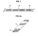
- the FFC did not require any type of characteristic impedance or electrical characteristics. Due to this the FFC, as shown in Figure 1, has a core conductor 101 affixed from both sides by the base film 103, made of polyethylene terephthalate and the like attached to the fixed adhesive layer 102, and when laminated is able to fulfill the necessary specification requirements solely through the adhesion of the base film 103 on both sides.
- EMI Electromagnetic Interference
- the formation of the shield layer as an EMI countermeasure does decrease the problems caused by noise but form the viewpoint of attempting to accelerate the signal transmission speed it is impossible to ignore the effect of transmission loss caused by the inability of impedance matching within the cable.
- reflection may occur in the cable due to the inability of impedance matching, leading to the reflected signal being emitted as noise outside of the cable.
- the shield is thought to be one of the causes of this type of reflection.
- This method is effective as an EMI countermeasure but, from the viewpoint of electrical characteristics, creates inconveniences such as a large increase in electrostatic capacity and a lowering of characteristic impedance due to the existence of a metallic body in proximity to the signal transmission conductor.
- physical measures such as decreasing the cross-sectional pile of the conductors, expanding the pitch between the conductors, and expanding the distance between the conductors and metallic bodies are effective but have a large effect on the specifications of the product and cannot be easily changed.
- the FFC has strict limitations placed on thickness and also when considering the stress placed on the FFC when flexing, a slimmer form is desirable.
- a slimmer form is desirable.
- Patent document 1 Japanese Patent Application Laid-Open No.20003-31033
- a flexible flat cable equipped with a metallic layer having an attached conductivity adhesive layer wherein a row of multiple conductors arranged in a parallel manner and a foam insulator with an adhesive layer that is laminated after sandwiching this row of conductors from both sides further sandwich a foam insulator having an adhesive agent on both sides is disclosed.
- this flexible flat cable due to the lamination of the foam insulator having sandwiched the row of conductors at both ends, the dielectric constant of the foam insulator is combined with the dielectric constant of the air allowing the combined dielectric constant to be lower than the dielectric constant of the insulator that is not yet foaming, making it possible to regulate the electrostatic capacity which is the characteristic impedance factor and make the characteristic impedance factor 50 Ohms. Furthermore, with this flexible flat cable the foam insulator is relatively large having a thickness of 150 ⁇ m to 250 ⁇ m and for the metallic layer having an attached conductivity adhesive layer, a metallic layer laminated with aluminum foil and base film is used.
- the present invention in consideration of the circumstances, is presented with the objective of being a flexible flat cable, which while maintaining the effect of the shield does not lose the electrical characteristics, also appropriate for use with existing connecters, and making matching electrical characteristics by means of existing processes.
- the invented flexible flat cable furthermore, is capable of being established with any number of wires, any length of cable, and any alignment of wiring.
- the flexible flat cable of this invention has the feature of being devised with attention given to the dielectric constant and thickness of the insular material as well as the effects of the shield layer material upon the impedance.
- the flexible flat cable of the present invention that fulfills the aforementioned objective is equipped with an arrangement of multiple conductors arranged to include a signal line and at least one ground line, first and second insular materials sandwiching the multiple conductors from both ends, shield material attached to a side of the first insular material opposite to the multiple conductors, the shield material being conductive via a conductive adhesive agent with the ground line out of the multiple conductors, and a reinforcement board attached to the side of the second insular material opposite the multiple conductors.
- the multiple conductors each having a conducting width from 0.3 ⁇ 0.03mm, are arranged in a parallel manner with a pitch of 0.5 ⁇ 0.05mm
- the first insular material is porous polyethylene trephthalate made of, starting from the side affixed to the shield material, a polyethylene trephthalate film, a substantially 34 ⁇ m thick porous layer, and an insular adhesive layer
- the shield material is made in a laminating manner, starting from the side affixed to the first insular material, of a conductive adhesive layer made of the conductive adhesive agent, a shield layer made of a polymer-based conductive layer less than 20 ⁇ m thick that is a prescribed resin formed including air with uniformly dispersed conductive particles, and base film.
- the flexible flat cable of this type of invention uses porous polyethylene trephthalate having a porous layer with a thickness of substantially 34 ⁇ m as the first insular material. Therefore, in the flexible flat cable of the present invention, by the combination of the dielectric constant of the insular material and the dielectric constant of the air containing the porous layer, the dielectric constant becomes comparatively lower than that of insular material not containing a porous layer. Accordingly, in the flexible flat cable of the present invention, regulation of the electrostatic capacity determined by differential impedance is possible due to the decrease in the dielectric constant.
- the differential impedance and the electrostatic capacity created by the space between the conductor and the shield layer can be regulated by using a polymer-based conductive layer containing air with a thickness no greater than 20 ⁇ m and containing uniformly dispersed conductive particles in a prescribed resin, as the shield material.
- the shield it is desirable for the shield to have a thickness of 10 ⁇ m, so that the differential impedance becomes 100 Ohms.
- the shield material prefferably has a surface resistivity equal to or below 10 Ohms/square and it is further desirable that the porous layer have a porous ratio of approximately 22%.
- conductive carbon can be used as the conductive particle contained in the shield layer and butylene rubber, polyester, urethane, or the like can be used as the resin forming the shield layer.
- the laminated base film and insular adhesive layer can be used as the second insular material.
- soft copper that has received surface processing by a prescribed metal plating of tin and such can be used for each of the conductors.
- the base film and insular adhesive layer that have been laminated can be used as the reinforcement board.
- the present invention as described above makes it possible to regulate the electrostatic capacity through the use of shield material having low dielectric constant insular material and polymer-based conductive layer, and as a result is able to avoid a decrease in differential impedance and achieve the desired value of 100 Ohms. Accordingly, the present invention is able to maintain the shield effect while avoiding the loss of electrical characteristics. Also, the present invention can be manufactured inexpensively due to its ability to match with electrical characteristics by existing processes and its compatibility with existing connecters, and furthermore can be established with any number of wires, cable length, and wiring arrangement.
- This embodiment is a flexible flat cable (Flexible Flat Cable; hereinafter referred to as FFC) used as a connecting cable in various internal systems disposed within various electrical products.
- FFC Flexible Flat Cable
- This FFC is especially suitable for high frequency and, as a result of the committed research of the inventors and the selection of structure and materials, has attained the ability to maintain the shield effect without losing the electrical characteristics.
- PET porous polyethylene trephthalate
- this FFC 10 is constructed in a manner such that multiple conductors 11, arranged in a parallel manner with a pitch of 0.5 ( ⁇ 0.05)mm, are laminated after being sandwiched between the first insular material 12 having an attached adhesive agent and the second insular material 13, and the shield material 14 is adhered to the side of the first insular material 12 opposite the conductors 11 by whereas the prescribed reinforcement board15 is adhered to the side of the second insular material 13 opposite the conductors 11.
- the shield material 14 and the conductors that become the ground line out of the multiple conductors are made conductive by connecting with each other via the conductive adhesive agent 16.
- the conductors 11 used are soft copper with a width of 0.3 ( ⁇ 0.03)mm and a thickness of 0.035mm that has received surface processing through tin plating.
- the first insular material 12 as a low dielectric material used is a porous PET having a total width of 68 ⁇ m and made in a laminating manner, starting form the side attached to the shield material 14, of a PET film 21 made of 4 ⁇ m thick base film, a 34 ⁇ m thick porous layer 22, and a 30 ⁇ m thick insular adhesive layer 23 as shown in Fig. 4.
- the second insular material 13 used is, in a laminating manner starting form the side attached to the reinforcement board15, PET film 24 made of 12 ⁇ m thick base film and a 25 ⁇ m thick insular adhesive layer 25.
- the shield material 14 used is evaporated silver shield material made in a laminating manner, starting from the side attached to the first insular material 12, of a 20 ⁇ m thick conductive adhesive layer16, a 0.1 ⁇ m thick evaporation coating layer 26, and a PET film 27 made of 9 ⁇ m thick base film having been laminated with a combined thickness of 29.1 ⁇ m.
- This FFC 10 as shown in Fig.
- the inventors using this type of the FFC, measured the characteristic impedance and differential impedance through the so-called TDR (Time Domain Reflectometry) method. Through this measurement, with three prescribed points of the transmission path set as the measurement points, the average value of the measurement results of these measurement points is calculated. The measurement results are shown in the following Table 2. It is to be noted that, the TDR method is able to measure electromagnetic waves caused by high frequency band range with a range of 1MHz to 30 GHz and display the wave shape along a time axis.
- TDR Time Domain Reflectometry
- Table 2 MEASUREMENT RESULTS Materials Used Characteristic impedance (Ohms) Differential Impedance (Ohms) Electrostatic Capacity (at 1MHz) (pF/m) Insular Material Shield Material Porous PET Evaporated Silver PET 50.0 81.3 192
- the FFC 10 is able to attain matching of the electrical characteristics and make the characteristic impedance 50 Ohms by using the porous PET as the first insular material 12 and evaporated silver shield material as the shield material 14.
- This type of the FFC 10 can be inexpensively manufactured with existing equipment due to its ability to be manufactured through existing manufacturing processes.
- the inventors further modified this FFC 10 and attempted to gain much larger characteristic impedance and set the differential impedance near 100 Ohms.
- the inventors used the porous PET for the insular material in the same way as the FFC 10 but used a polymer-based-based material for the shield material.
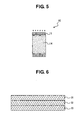
- the polymer-based shield material as shown in Fig. 6, has a three-layered structure comprising a PET film 31 serving as the base film, a polymer-based-based conductive layer 32 as the shield layer, and a conductive adhesive layer 33.
- the polymer-based-based conductive layer 32 is interfused with uniformly dispersed conductive particles of conductive carbon and the like in the prescribed resin of butylene rubber and polyester, urethane and the like.
- a shield layer formed in a membranous shape is generally used as the shield material but the polymer-based-based shield material does not have a shield layer formed in a membranous shape but rather has a polymer-based conductive layer 32 formed in a manner including air by which, from the viewpoint of electrical characteristics, attains characteristics equivalent to a metallic mesh membrane. That is to say, the polymer-based shield material does not have a uniform membranous shield layer and due to its existence with air has anisotropic properties and allows a wider distance between the conductors than shield material made from an evaporated metallic body, and is different from simple metallic shielding material in that it is advantageous in the regulation of electrical characteristics.
- the inventors were able to regulate the electrical characteristics by the construction of appropriately dispersed conductive particles and also, through the use of polymer-based shield material able to attain the shield effect, attempted to increase the characteristic impedance.
- the inventors experimentally produced an FFC 50 like that shown in Fig. 7 using the specifications shown in Table 3 for the conductors, the insular material, and the reinforcement board and using specifications shown in Table 4 for the shield material.
- this FFC 50 is constructed in a manner such that multiple conductors 51, arranged in a parallel manner with a pitch of 0.5 ( ⁇ 0.05)mm, are laminated after being sandwiched between a first insular material 52 having an attached adhesive agent and a second insular material 53.
- the shield material 54 is adhered to the side of the first insular material 52 opposite the conductors 51 whereas the prescribed reinforcement board 55 is adhered to the side of the second insular material 53 opposite the conductors 51.
- the shield material 54 and the conductor 51 that become the ground line out of the multiple conductors 51 are made conductive via the conductive adhesive agent 56.
- the conductors 51 used are soft copper with a width of 0.3 ( ⁇ 0.03)mm and a thickness of approximately 0.035mm that has received surface processing through tin plating.
- the first insular material 52 as a low dielectric material used is a porous PET having a total width of substantially 68 ⁇ m and made of, in a laminating manner starting form the side attached to the shield material 54, a PET film 61 made of 4 ⁇ m thick base film, a 34 ⁇ m thick porous layer 62, and a 30 ⁇ m thick insular adhesive layer 63 as shown in Fig. 8.
- the second insular material 53 used is, in a laminating manner starting form the side attached to the reinforcement board 55, a PET film 64 made of 35 ⁇ m thick base film and a 25 ⁇ m thick insular adhesive layer 65.
- the reinforcement board 55 used is, in a laminating manner starting from the side attached to the second insular material 53, a 40 ⁇ m thick insular adhesive layer 66 and a 188 ⁇ m thick PET.
- the shield material 54 used is a polymer-based shield material made, in a laminating manner starting from the side attached to the first insular material 52, of a 35 ⁇ m thick conductive adhesive layer 56, a 22 ⁇ m thick polymer-based conductive layer 68, and a PET film 69 made of 25 ⁇ m thick base film with a combined thickness of 82 ⁇ m.
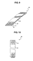
- This FFC 50 as shown in Fig. 9 and Fig. 10 with an arrangement of a ground line (G), a signal line (S), a signal line (S), a ground line (G), a signal line (S), a signal line (S), etc. and including a signal line and at least one ground line, has a wiring arrangement suitable for differential transmissions.
- an FFC using an evaporated silver shield layer comprising a laminated 20mm thick conductive adhesive layer and 9mm thick PET film with 0.1mm thick evaporated silver for a total thickness of 29.1mm
- an FFC using an evaporated aluminum shield layer comprising a laminated 25mm thick conductive adhesive layer and 12mm thick PET film with 0.06mm thick evaporated aluminum for a total thickness of 37.06mm
- an FFC with no shield material equipped for comparative purposes, the inventors experimentally produced an FFC using an evaporated silver shield layer comprising a laminated 20mm thick conductive adhesive layer and 9mm thick PET film with 0.1mm thick evaporated silver for a total thickness of 29.1mm
- an FFC using an evaporated aluminum shield layer comprising a laminated 25mm thick conductive adhesive layer and 12mm thick PET film with 0.06mm thick evaporated aluminum for a total thickness of 37.06mm
- an FFC with no shield material equipped for comparative purposes, the inventors experimentally produced an FFC using an evaporated silver shield layer comprising a laminated 20mm thick
- the inventors using this type of FFC 50 and the experimentally produced FFC for comparative purposes, conducted characteristic impedance, differential impedance, electrostatic capacity, and eye pattern measurements.
- the eye pattern was measured using the differential transmission method by a sampling oscilloscope (Model: 86100A) and pulse generator (Model: 81133A), both produced by the Agilent Technologies company, and, along with a measured frequency range of 400MHz, a wave frequency with a rising edge introduced at 2.5 ns was determined.
- Fig. 11(a) shows the eye pattern measurement results of an FFC using evaporated silver shield material as the shield material
- Fig. 11(b) shows the eye pattern measurement results of an FFC using evaporated aluminum shield material as the shield material
- Fig. 11(c) shows the eye pattern measurement results of an FFC 50 using polymer-based shield material as the shield material.
- Table 5 MEASUREMENT RESULTS Experimentally Produced Product-type Cable Length (mm) Material Used Average Value of Characteristic impedance (Ohms) Average Value of Differential Impedance (Ohms) Electrostatic Capacity (at 1MHz) (p F/m) Insular Layer Shield Layer Without Shield Material 200 Porous PET None 93.8 141.2 48.5 92.6 140.8 50.5 Evaporated Silver 38.7 61.9 205.0 39.2 62.0 204.5 38.2 61.7 205.0 38.5 62.7 207.5 With Shield Material Evaporated Aluminum 44.0 64.3 200.5 44.2 65.8 203.5 Polymer-based Shield Material 72.2 110.9 121.5 71.2 110.5 131.0
- the various types of experimentally produced FFCs can be thought of as having electrical merging between two adjacent conductors at the time of differential signal transmission due to the close proximity of the space between the conductors having a pitch of 0.5( ⁇ 0.05)mm.
- the differential impedance should be, in theory, double the characteristic impedance but, as shown in Table 5, is stuck at a value of approximately 1.5 times to 1.6 times.
- the occurrence of electrical loss caused by the electrical merging occurring between the adjacent conductors can be thought of as the reason for this.
- the FFC 50 using polymer-based shield material as the shield material results in a characteristic impedance 30 Ohms greater and a differential impedance 45 Ohms greater than other FFCs.
- This type of the FFC 50 is constructed using, aside from the shield material, the same materials as other FFCs making it effective both for avoiding a decrease in impedance and as a counter-measure to unnecessary radiation (Electromagnetic Interference; EMI).
- EMI Electromagnetic Interference
- the FFC 50 through the use of polymer-based shield material as the shield material, is able to regulate the electrical characteristics while avoiding these inconveniences, provide an effective counter-measure for unnecessary radiation, and maintain favorable mobility.
- Fig. 12 The measurement results of the attenuating rate by the electrical field from the simple shield material used in an experimentally produced FFC are shown in Fig. 12.
- the wave frequency (from 1MHz to 1GHz) is shown on the horizontal axis and the attenuating rate is shown on the vertical axis.
- the attenuating rate by the electrical field of polymer-based shield material is smaller than that of other membranous shield materials made from evaporated aluminum shield material or evaporated silver shield material. This is due to interfusion of uniformly dispersed conductive particles of conductive carbon and the like in the resin of butylene rubber and the like by the polymer-based conductive shield and this data is able to confirm that the shield layer possesses properties equivalent to a mesh-like shield layer.
- the FFC it is ideal to have both a shield effect and electrical traits but, in situations where the wiring is closely packed like a situation where the wiring pitch of the conductors is narrow or the thickness of the cable is thin, the conflicting relationship of the shield effect and electrical traits makes the combination of the two difficult and narrows the maintainable and combinable range of favorable traits from both a physical and electrical viewpoint.
- the polymer-based shield material even under the strict specifications mentioned above, possesses properties equivalent to a mesh-like membrane and is therefore extremely effective.
- the inventors further improved this type of FFC 50 and attained an FFC able to achieve differential impedance of 100 Ohms as shown in the embodiment of the present invention and achieved precise impedance regulation through the identification of materials and adjustment of width of the polymer-based conductive layer.
- the inventors used the specifications shown in the following Table 6 for the conductors and reinforcement board along with the specifications shown in the following Table 7 for the insular material. Also, the inventors experimentally produced, as shown in the following Table 8, FFCs using each of two types of polymer-based shield material having polymer-based conductive layers of dispersed carbon shield layers with electrical particles and having thicknesses of 10 ⁇ m and 20 ⁇ m, evaporated silver shield material possessing a 0.1 ⁇ m thick evaporated silver layer, and copper foil shield material possessing a 9 ⁇ m thick copper foil layer, for the shield material.
- the combinations shown in the following Table 9 were used for the first and second embodiments and the combinations shown in the following Table 10 were used for the first through eighth comparative examples.
- the porous layer made by porous PET has a porous ratio of 22% and the polymer-based shield material has a surface resistivity below 10 Ohms/square.
- the inventors measured the differential impedance and eye pattern using these types of FFCs.
- a sampling oscilloscope Model: HP54750A
- a TDR module Model: HP54754
- a measurement probe Model: ACP40 series GS500/SG500
- the eye pattern was measured using the differential transmission method by a sampling oscilloscope (Model: 86100A) and pulse generator (Model: 81133A), both produced by the Agilent Technologies company, and, along with a measured frequency range of 400MHz, a wave frequency with a rising edge introduced at 2.5 ns was determined.
- the differential impedance measurement results of all the embodiments and comparative examples are shown above in Table 9 and Table 10.
- the eye pattern measurement results of the embodiments and comparative examples are shown in Fig. 13(a) and Fig. 13(b).
- the eye pattern measurement results it is understood that in the first embodiment jitter is low and the eye pattern is clear making it sufficiently appropriate for high speed transmissions.
- the first comparative example it is understood that the eye pattern is unclear and signal reflection occurs in the transmission path due to the lack of impedance matching.
- the impedance mismatch results in the eye pattern being unclear.
- the impedance is affected by the thickness and permittivity of the insular material and the material of the shield layer.
- the porous PET through the combination of the permittivity of the insular material and the permittivity of the porous layer containing air, has lower permittivity compared to insular layers conventionally used in FFCs not containing air. Accordingly, in an FFC using porous PET as the insular material, it is possible to regulate the electrostatic capacity that determines the differential impedance and set the differential impedance to 100 Ohms due to the decrease in permittivity.
- the material of the shield material laminated above the insular material is an important factor for regulating the electrostatic capacity.
- the regulation of differential impedance is based on a fixed prescribed material for the shield material in the FFC
- compatibility with conventional FFCs is lost and it becomes necessary to use specialized connection shapes for terminal connectors.
- the cable itself is changed causing problems at the time of implementation.
- the FFC using polymer-based shield material of uniformly dispersed conductive carbon in a resin as the shield material, compared to membranous or mesh-like shield materials, it is possible to regulate and lower the electrostatic capacity occurring between the conductors and the shield layer while preserving favorable mobility and compatibility with existing connectors, which results in the ability to set the differential impedance to 100 Ohms.
- an impedance of 100 Ohms can be realized only in an FFC cable with an insular layer of suitable thickness and permittivity important for regulating the impedance, a suitable combination of materials for the shield material, porous PET that is a 34 ⁇ m thick porous layer for the insular material, and polymer-based shield material serving as a shield layer made of dispersed conductive carbon for the conductive particles with a thickness below 20 ⁇ m, desirably 10 ⁇ m, for the shield material.
- the FFC due to the structure of the insular material and shield material in the FFC it is unnecessary to have special surface treatment in order to connect to the terminal connecter. Further, the FFC can be manufactured inexpensively and without incurring initial cost due to its ability to be used by existing manufacturing processes and be combined with electrical characteristics by existing manufacturing processes. Furthermore, it is possible for the FFC to have the number of wires, cable length, and wire arrangement containing a conductive ground line with a shield layer set up in any manner.
- This type of FFC is ideally suitable for all types of electrical equipment products that require high speed transmission of a signal, for example liquid crystal monitor systems requiring the transmission of high-definition images and, while maintaining the shield effect, is able to avoid damaging the electrical characteristics and, from the perspective of its superior physical characteristics, enables the miniaturization of the electrical equipment products.
Landscapes
- Insulated Conductors (AREA)
- Communication Cables (AREA)
Abstract
The FFC (50) comprises multiple conductors (51) with widths of 0.3(±0.03)mm arranged in a parallel manner with a pitch of 0.5 (± 0.05)mm, the first insular material (52) and the second insular material (53) sandwiching these conductors (51) from both sides, shield material (54), and the reinforcement board (55). The first insular material (52) is porous PET possessing a 34µm thick porous layer (62) and the shield material (54) is a polymer-based shield material possessing a shield layer made of a polymer-based conductive layer (69) equal to or less than 20µm thick that is a prescribed resin formed including air with uniformly dispersed conductive particles. Due to this, the FFC (50) maintains the shield effect without damaging the electrical characteristics and also, along with being compatible with existing connecters, can combine with the electrical traits by existing processes and furthermore is capable of being established with any number of wires, any length of cable, and any alignment of wiring.
Description
- The present invention relates to a flexible flat cable used as a connecting cable in a variety of parts internally disposed within a variety of electrical products.
- Conventionally, a so-called flexible flat cable (Flexible Flat Cable; hereinafter referred to as FFC) is often used as a connecting cable internally disposed within various electrical products, especially printers and scanners. Due to its superior flexibility, the FFC can be used in moving parts and furthermore, when compared to the flexible print circuit (Flexible Print Circuit; FPC), has a lower manufacturing cost which leads to lower cost per unit, making it applicable in a wide range of fields.
- It is to be noted that conventionally, the FFC did not require any type of characteristic impedance or electrical characteristics. Due to this the FFC, as shown in Figure 1, has a
core conductor 101 affixed from both sides by thebase film 103, made of polyethylene terephthalate and the like attached to the fixedadhesive layer 102, and when laminated is able to fulfill the necessary specification requirements solely through the adhesion of thebase film 103 on both sides. - To the contrary, in recent years the development of electrical products that realized increased high definition quality of graphics such as notebook style personal computers and digital scanners has been accompanied by a demand for an increase in the speed of signal transmissions. Furthermore, even in the case of other electrical products, as progressing towards digitalization, those products raise imperative technological problems in increased speed of signal transmissions.
- Generally, when a signal transmission cable does a high speed signal transmission, the cable lowers the resistance to noise, so that a high speed signal transmission comes to be demanded. However, with this cable, the acceleration of the signal transmission speed may raise the problem of unnecessary radiation (Electromagnetic Interference; EMI). In other words, by this method of signal transmission where the signal wave frequency is high, EMI noise (electromagnetic waves) becomes easily leaked causing noise to enter into the neighboring cables, which is known to cause such adverse effects as malfunctions and transmission loss of signal.
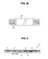
- To the contrary, from the idea that if the source of noise generation can be sealed in a metallic film then the noise will not leak, a countermeasure is commonly undertaken whereby the outer circumference of the FFC product, as shown in Figure 2(a) and Figure 2(b), is formed with a
shield layer 105 whereinmultiple conductors 106 are established linearly and any given conductor is connected to theappropriate shield layer 105 which in turn is connected to a ground line (G). However, this shield does not regulate electrical characteristics. - In other words, with this signal transmission cable, the formation of the shield layer as an EMI countermeasure does decrease the problems caused by noise but form the viewpoint of attempting to accelerate the signal transmission speed it is impossible to ignore the effect of transmission loss caused by the inability of impedance matching within the cable. With this cable, reflection may occur in the cable due to the inability of impedance matching, leading to the reflected signal being emitted as noise outside of the cable.
- The shield is thought to be one of the causes of this type of reflection. In other words, with this cable, it is necessary to use metallic plates or metallic films as a shielding plate in order to prevent noise leakage to the outside. This method is effective as an EMI countermeasure but, from the viewpoint of electrical characteristics, creates inconveniences such as a large increase in electrostatic capacity and a lowering of characteristic impedance due to the existence of a metallic body in proximity to the signal transmission conductor. As a method for lowering this type of electrostatic capacity, physical measures such as decreasing the cross-sectional pile of the conductors, expanding the pitch between the conductors, and expanding the distance between the conductors and metallic bodies are effective but have a large effect on the specifications of the product and cannot be easily changed. Further, due to mobility requirements, the FFC has strict limitations placed on thickness and also when considering the stress placed on the FFC when flexing, a slimmer form is desirable. Of course with an FFC it is conceivable to remove the shield that causes the decrease of impedance, but this would be rash to simply remove the shield due to the effect of the noise.
- In the manner described above, with this cable, it especially becomes extremely difficult to make an FFC appropriate for high speed transmission due to the shield equipped as a noise countermeasure, because the shield layer may impair the electrical property of the cable.
- Furthermore, with the FFC, there is tested characteristic impedance regulation technology, such as that described in patent document 1.
- Patent document 1:
Japanese Patent Application Laid-Open No.20003-31033 - Specifically, in this patent document 1, a flexible flat cable equipped with a metallic layer having an attached conductivity adhesive layer wherein a row of multiple conductors arranged in a parallel manner and a foam insulator with an adhesive layer that is laminated after sandwiching this row of conductors from both sides further sandwich a foam insulator having an adhesive agent on both sides is disclosed. In this manner, this flexible flat cable, due to the lamination of the foam insulator having sandwiched the row of conductors at both ends, the dielectric constant of the foam insulator is combined with the dielectric constant of the air allowing the combined dielectric constant to be lower than the dielectric constant of the insulator that is not yet foaming, making it possible to regulate the electrostatic capacity which is the characteristic impedance factor and make the
characteristic impedance factor 50 Ohms. Furthermore, with this flexible flat cable the foam insulator is relatively large having a thickness of 150µm to 250µm and for the metallic layer having an attached conductivity adhesive layer, a metallic layer laminated with aluminum foil and base film is used. - It is to be noted that many high frequency cables taking into consideration the effect of the shield and electrical characteristics, mostly extremely fine coaxial cables and the like, are being sold, but for a high price and furthermore use specialized connecters which, accompanied by the specialized terminal furnishment necessary for connecting the connecters, require a large amount of wiring production costs and have poor effectiveness making them not generally applicable when compared to the FPC connecters. Furthermore, the high frequency waves are generally classified by MHz bandwidth and GHz bandwidths, but the high frequency cables being sold have specifications that are usable with GHz bandwidths. Because of this regardless of the fact that only the MHz bandwidth is to be used, it is necessary in actuality to use an expensive cable with a GHz bandwidth, imposing a large burden of cost. Also, the technology described above in Patent Document 1, having the objective of regulating the characteristic impedance in general high frequency circuits to an appropriate level of 50 Ohms, is completely inappropriate for machines that require other types of characteristic impedance and differential impedance.
- Accordingly, with cables following the FFC, it is anticipated that it will be possible to show high effects from the shield without incurring losses of the electrical characteristics and the desired differential impedance will be able to be realized.
- The present invention, in consideration of the circumstances, is presented with the objective of being a flexible flat cable, which while maintaining the effect of the shield does not lose the electrical characteristics, also appropriate for use with existing connecters, and making matching electrical characteristics by means of existing processes. The invented flexible flat cable, furthermore, is capable of being established with any number of wires, any length of cable, and any alignment of wiring.
- The flexible flat cable of this invention has the feature of being devised with attention given to the dielectric constant and thickness of the insular material as well as the effects of the shield layer material upon the impedance.
- In other words, the flexible flat cable of the present invention that fulfills the aforementioned objective is equipped with an arrangement of multiple conductors arranged to include a signal line and at least one ground line, first and second insular materials sandwiching the multiple conductors from both ends, shield material attached to a side of the first insular material opposite to the multiple conductors, the shield material being conductive via a conductive adhesive agent with the ground line out of the multiple conductors, and a reinforcement board attached to the side of the second insular material opposite the multiple conductors. In the flexible flat cable, the multiple conductors, each having a conducting width from 0.3±0.03mm, are arranged in a parallel manner with a pitch of 0.5±0.05mm, the first insular material is porous polyethylene trephthalate made of, starting from the side affixed to the shield material, a polyethylene trephthalate film, a substantially 34µm thick porous layer, and an insular adhesive layer, and the shield material is made in a laminating manner, starting from the side affixed to the first insular material, of a conductive adhesive layer made of the conductive adhesive agent, a shield layer made of a polymer-based conductive layer less than 20µm thick that is a prescribed resin formed including air with uniformly dispersed conductive particles, and base film.
- The flexible flat cable of this type of invention uses porous polyethylene trephthalate having a porous layer with a thickness of substantially 34µm as the first insular material. Therefore, in the flexible flat cable of the present invention, by the combination of the dielectric constant of the insular material and the dielectric constant of the air containing the porous layer, the dielectric constant becomes comparatively lower than that of insular material not containing a porous layer. Accordingly, in the flexible flat cable of the present invention, regulation of the electrostatic capacity determined by differential impedance is possible due to the decrease in the dielectric constant.
- In addition, in the flexible flat cable of the present invention, the differential impedance and the electrostatic capacity created by the space between the conductor and the shield layer can be regulated by using a polymer-based conductive layer containing air with a thickness no greater than 20µm and containing uniformly dispersed conductive particles in a prescribed resin, as the shield material.
- Here, it is desirable for the shield to have a thickness of 10µm, so that the differential impedance becomes 100 Ohms.
- In addition, it is desirable for the shield material to have a surface resistivity equal to or below 10 Ohms/square and it is further desirable that the porous layer have a porous ratio of approximately 22%.
- Further, conductive carbon can be used as the conductive particle contained in the shield layer and butylene rubber, polyester, urethane, or the like can be used as the resin forming the shield layer.
- Yet further, starting from the side attached to the reinforcement board, the laminated base film and insular adhesive layer can be used as the second insular material.
- In addition, soft copper that has received surface processing by a prescribed metal plating of tin and such can be used for each of the conductors.
- Also, starting from the side attached to the second insular material, the base film and insular adhesive layer that have been laminated can be used as the reinforcement board.
- The present invention as described above makes it possible to regulate the electrostatic capacity through the use of shield material having low dielectric constant insular material and polymer-based conductive layer, and as a result is able to avoid a decrease in differential impedance and achieve the desired value of 100 Ohms. Accordingly, the present invention is able to maintain the shield effect while avoiding the loss of electrical characteristics. Also, the present invention can be manufactured inexpensively due to its ability to match with electrical characteristics by existing processes and its compatibility with existing connecters, and furthermore can be established with any number of wires, cable length, and wiring arrangement.
-
- Fig. 1 is a cross-sectional view explaining the FFC structure until now.
- Fig. 2(a) is a perspective view explaining the FFC structure until now having a shield layer formed around the circumference of the product to seal the source of noise generation with a metallic film.
- Fig. 2(b) is a planar view explaining the FFC structure until now shown in Fig. 2(a).
- Fig. 3 is a cross-sectional view explaining the structure of the experimentally produced FFC using evaporated silver shield material as a shield material.
- Fig. 4 is an exploded cross-sectional view explaining the detailed structure of the FFC shown in Fig. 3.
- Fig. 5 is a planar view explaining the structure of the FFC shown in Fig. 3.
- Fig. 6 is a cross-sectional view explaining the structure of the polymer-based shield material.
- Fig. 7 is a cross-sectional view explaining the structure of the experimentally produced FFC using polymer-based shield material as a shield material.
- Fig. 8 is an exploded cross-sectional view explaining the detailed structure of the FFC shown in Fig. 7.
- Fig. 9 is a perspective view explaining the structure of the FFC shown in Fig. 7.
- Fig. 10 is a planar view explaining the structure of the FFC shown in Fig. 7.
- Fig. 11(a) is a diagram showing the eye pattern measurement results using the experimentally produced FFC and the eye pattern measurement results from an FFC using shield material made from evaporated silver shield material.
- Fig. 11(b) is a diagram showing the eye pattern measurement results using the experimentally produced FFC and the eye pattern measurement results from an FFC using shield material made from evaporated aluminum shield material.
- Fig. 11(c) is a diagram showing the eye pattern measurement results using the experimentally produced FFC and the eye pattern measurement results from the FFC shown in Fig. 7 using shield material made from polymer-based shield material.
- Fig. 12 is a diagram showing the attenuating rate measurement results caused by the electric field of the simple shield material used in the experimentally produced FFC.
- Fig. 13(a) is a diagram showing the eye pattern measurement results of the experimentally produced FFC and the eye pattern results of the first embodiment.
- Fig. 13(b) is a diagram showing the eye pattern measurement results of the experimentally produced FFC and the eye pattern results of the comparative example.
- Hereinafter, specific embodiments to which the present invention is applied are described in detail with reference to the illustrations.
- This embodiment is a flexible flat cable (Flexible Flat Cable; hereinafter referred to as FFC) used as a connecting cable in various internal systems disposed within various electrical products. This FFC is especially suitable for high frequency and, as a result of the committed research of the inventors and the selection of structure and materials, has attained the ability to maintain the shield effect without losing the electrical characteristics.
- First, in order to clarify the present invention, the FFC achieved through the independent research of the inventors leading to the present invention will be described.
- The inventors, along with using porous polyethylene trephthalate (Hereinafter referred to as PET) as the insular material, composed an FFC using evaporated silver shield material with an attached conductive adhesive agent for the shield material and tested the matching of the electrical characteristics.
- This gives attention to the low drift due to temperature change and the low amount of change even by wide bandwidth of the conductive resistance of the conductive adhesive agent used as the shield material. Actually, the inventors, using specifications shown in the following Table 1 for conductors, insular materials and shield materials, experimentally produced an
FFC 10 as shown in Fig. 3. -
[Table 1] Material Surface Processing Size (mm) PET Thickness (µm) Insular Layer/Shield Layer Thickness (µm) Adhesive Layer Thickness (µm) Total Thickness (µm) Conductors Soft Copper Tin Plating Width: 0.3 Thickness: 0.035 - - - - Insular Material Porous PET - - 4 34 30 68 Shield Material Evaporated Silver PET - - 9 0.1 20 29.1 - In other words, this
FFC 10 is constructed in a manner such thatmultiple conductors 11, arranged in a parallel manner with a pitch of 0.5 (±0.05)mm, are laminated after being sandwiched between the firstinsular material 12 having an attached adhesive agent and the secondinsular material 13, and theshield material 14 is adhered to the side of the firstinsular material 12 opposite theconductors 11 by whereas the prescribed reinforcement board15 is adhered to the side of the secondinsular material 13 opposite theconductors 11. Theshield material 14 and the conductors that become the ground line out of the multiple conductors are made conductive by connecting with each other via the conductiveadhesive agent 16. - More specifically, the
conductors 11 used are soft copper with a width of 0.3 (± 0.03)mm and a thickness of 0.035mm that has received surface processing through tin plating. Also, the firstinsular material 12 as a low dielectric material used is a porous PET having a total width of 68µm and made in a laminating manner, starting form the side attached to theshield material 14, of aPET film 21 made of 4µm thick base film, a 34µm thickporous layer 22, and a 30µm thick insularadhesive layer 23 as shown in Fig. 4. Further, as shown in the same diagram, the secondinsular material 13 used is, in a laminating manner starting form the side attached to the reinforcement board15,PET film 24 made of 12µm thick base film and a 25µm thick insularadhesive layer 25. Furthermore, as shown in the same diagram, theshield material 14 used is evaporated silver shield material made in a laminating manner, starting from the side attached to the firstinsular material 12, of a 20µm thick conductive adhesive layer16, a 0.1µm thickevaporation coating layer 26, and aPET film 27 made of 9µm thick base film having been laminated with a combined thickness of 29.1µm. ThisFFC 10, as shown in Fig. 5 with an arrangement of a ground line (G), a signal line (S), a signal line (S), a ground line (G), a signal line (S), a signal line (S), etc. and including a signal line and at least one ground line, has a wiring arrangement suitable for differential transmissions. - The inventors, using this type of the FFC, measured the characteristic impedance and differential impedance through the so-called TDR (Time Domain Reflectometry) method. Through this measurement, with three prescribed points of the transmission path set as the measurement points, the average value of the measurement results of these measurement points is calculated. The measurement results are shown in the following Table 2. It is to be noted that, the TDR method is able to measure electromagnetic waves caused by high frequency band range with a range of 1MHz to 30 GHz and display the wave shape along a time axis.
- [Table 2]
Table 2 MEASUREMENT RESULTS Materials Used Characteristic impedance (Ohms) Differential Impedance (Ohms) Electrostatic Capacity (at 1MHz) (pF/m) Insular Material Shield Material Porous PET Evaporated Silver PET 50.0 81.3 192 - In the manner described above, the
FFC 10 is able to attain matching of the electrical characteristics and make thecharacteristic impedance 50 Ohms by using the porous PET as the firstinsular material 12 and evaporated silver shield material as theshield material 14. This type of theFFC 10 can be inexpensively manufactured with existing equipment due to its ability to be manufactured through existing manufacturing processes. - Furthermore, the inventors further modified this
FFC 10 and attempted to gain much larger characteristic impedance and set the differential impedance near 100 Ohms. Specifically, the inventors used the porous PET for the insular material in the same way as theFFC 10 but used a polymer-based-based material for the shield material. - The polymer-based shield material, as shown in Fig. 6, has a three-layered structure comprising a
PET film 31 serving as the base film, a polymer-based-basedconductive layer 32 as the shield layer, and a conductiveadhesive layer 33. The polymer-based-basedconductive layer 32 is interfused with uniformly dispersed conductive particles of conductive carbon and the like in the prescribed resin of butylene rubber and polyester, urethane and the like. Here, a shield layer formed in a membranous shape is generally used as the shield material but the polymer-based-based shield material does not have a shield layer formed in a membranous shape but rather has a polymer-basedconductive layer 32 formed in a manner including air by which, from the viewpoint of electrical characteristics, attains characteristics equivalent to a metallic mesh membrane. That is to say, the polymer-based shield material does not have a uniform membranous shield layer and due to its existence with air has anisotropic properties and allows a wider distance between the conductors than shield material made from an evaporated metallic body, and is different from simple metallic shielding material in that it is advantageous in the regulation of electrical characteristics. - In the manner described above, the inventors were able to regulate the electrical characteristics by the construction of appropriately dispersed conductive particles and also, through the use of polymer-based shield material able to attain the shield effect, attempted to increase the characteristic impedance. Actually, the inventors experimentally produced an
FFC 50 like that shown in Fig. 7 using the specifications shown in Table 3 for the conductors, the insular material, and the reinforcement board and using specifications shown in Table 4 for the shield material. - [Table 3]

- [Table 4]

- In other words, this
FFC 50 is constructed in a manner such thatmultiple conductors 51, arranged in a parallel manner with a pitch of 0.5 (±0.05)mm, are laminated after being sandwiched between a firstinsular material 52 having an attached adhesive agent and a secondinsular material 53. Theshield material 54 is adhered to the side of the firstinsular material 52 opposite theconductors 51 whereas the prescribedreinforcement board 55 is adhered to the side of the secondinsular material 53 opposite theconductors 51. Theshield material 54 and theconductor 51 that become the ground line out of themultiple conductors 51 are made conductive via the conductiveadhesive agent 56. - More specifically, in a manner similar to that of
FFC 10, theconductors 51 used are soft copper with a width of 0.3 (±0.03)mm and a thickness of approximately 0.035mm that has received surface processing through tin plating. Also, the firstinsular material 52 as a low dielectric material used is a porous PET having a total width of substantially 68µm and made of, in a laminating manner starting form the side attached to theshield material 54, aPET film 61 made of 4µm thick base film, a 34µm thickporous layer 62, and a 30µm thick insularadhesive layer 63 as shown in Fig. 8. Further, as shown in the same diagram, the secondinsular material 53 used is, in a laminating manner starting form the side attached to thereinforcement board 55, aPET film 64 made of 35µm thick base film and a 25µm thick insularadhesive layer 65. Furthermore, as shown in the same diagram, thereinforcement board 55 used is, in a laminating manner starting from the side attached to the secondinsular material 53, a 40µm thick insularadhesive layer 66 and a 188µm thick PET. In addition, as shown in the same diagram, theshield material 54 used is a polymer-based shield material made, in a laminating manner starting from the side attached to the firstinsular material 52, of a 35µm thick conductiveadhesive layer 56, a 22µm thick polymer-basedconductive layer 68, and aPET film 69 made of 25µm thick base film with a combined thickness of 82µm. ThisFFC 50, as shown in Fig. 9 and Fig. 10 with an arrangement of a ground line (G), a signal line (S),a signal line (S), a ground line (G), a signal line (S), a signal line (S), etc. and including a signal line and at least one ground line, has a wiring arrangement suitable for differential transmissions. - In addition, for comparative purposes, the inventors experimentally produced an FFC using an evaporated silver shield layer comprising a laminated 20mm thick conductive adhesive layer and 9mm thick PET film with 0.1mm thick evaporated silver for a total thickness of 29.1mm, an FFC using an evaporated aluminum shield layer comprising a laminated 25mm thick conductive adhesive layer and 12mm thick PET film with 0.06mm thick evaporated aluminum for a total thickness of 37.06mm, and an FFC with no shield material equipped.
- The inventors, using this type of
FFC 50 and the experimentally produced FFC for comparative purposes, conducted characteristic impedance, differential impedance, electrostatic capacity, and eye pattern measurements. - The characteristic impedance and differential impedance, with three prescribed points of the transmission path set as the measurement points, were measured by the TDR method using a sampling oscilloscope (Model: HP54750A) and a TDR module (Model: HP54754), both produced by the Hewlett-Packard company, and the average value of these measurement results was determined. Also, the electrostatic capacity was measured, having been swept with a frequency from 1MHz to 1.8GHz by an impedance analyzer (Model: 4291B) produced by the Agilent Technologies company, and a measurement value of 1MHz was determined. Further, the eye pattern was measured using the differential transmission method by a sampling oscilloscope (Model: 86100A) and pulse generator (Model: 81133A), both produced by the Agilent Technologies company, and, along with a measured frequency range of 400MHz, a wave frequency with a rising edge introduced at 2.5 ns was determined.
- The measurement results of the characteristic impedance, differential impedance, and electrostatic capacity are shown in the following Table 5. Also, the measurement results of the eye pattern are shown in Fig. 11(a) and Fig. 11(c). In addition, Fig. 11(a) shows the eye pattern measurement results of an FFC using evaporated silver shield material as the shield material, Fig. 11(b) shows the eye pattern measurement results of an FFC using evaporated aluminum shield material as the shield material, and Fig. 11(c) shows the eye pattern measurement results of an
FFC 50 using polymer-based shield material as the shield material. - [Table 5]
Table 5 MEASUREMENT RESULTS Experimentally Produced Product-type Cable Length (mm) Material Used Average Value of Characteristic impedance (Ohms) Average Value of Differential Impedance (Ohms) Electrostatic Capacity (at 1MHz) (p F/m) Insular Layer Shield Layer Without Shield Material 200 Porous PET Nothing 93.8 141.2 48.5 92.6 140.8 50.5 Evaporated Silver 38.7 61.9 205.0 39.2 62.0 204.5 38.2 61.7 205.0 38.5 62.7 207.5 With Shield Material Evaporated Aluminum 44.0 64.3 200.5 44.2 65.8 203.5 Polymer-based Shield Material 72.2 110.9 121.5 71.2 110.5 131.0 - From these measurement results it is understood that through the FFC using evaporated aluminum and evaporated silver shield material for the shield material, the decrease in impedance originating from the increase in electrostatic capacity is due to the introduction of a metallic membrane. On the other hand, it is understood that through the
FFC 50 using polymer-based shield material for the shield material, the decrease of impedance is avoidable due to the electrostatic capacity of approximately 80pF/m, which is comparatively lower than that of other FFCs. - From the eye pattern measurement results it is understood that through the
FFC 50 using polymer-based shield material for the shield material it is possible to attain sufficient compatibility with a 400MHz signal transmission due to the low jitter and clear eye pattern of theFFC 50 compared to other FFCs. In addition, the inventors measured the eye pattern with a measured frequency range of 2.5GHz and a wave frequency with a rising edge introduced at 400ps but in this situation, not shown, through anFFC 50 using polymer-based shield material as the shield material the jitter increased but the eye pattern could be clearly seen and the possibility for compatibility with a signal transmission of 2.5GHz was confirmed. - Here, in a situation where two conductors transmitting differential signals with a characteristic impedance Zo of 50 Ohms are arranged with sufficient separation, the differential impedance becomes 2 × Z0=100 Ohms but two conductors placed in close proximity lead to electrical merging which is known to lower the differential impedance between the conductors. Accordingly, in a situation where two conductors are arranged in close proximity in an FFC, for such reasons as increasing the wire density, a decrease in impedance occurs.
- From this viewpoint, the various types of experimentally produced FFCs can be thought of as having electrical merging between two adjacent conductors at the time of differential signal transmission due to the close proximity of the space between the conductors having a pitch of 0.5(±0.05)mm. As described above, the differential impedance should be, in theory, double the characteristic impedance but, as shown in Table 5, is stuck at a value of approximately 1.5 times to 1.6 times. The occurrence of electrical loss caused by the electrical merging occurring between the adjacent conductors can be thought of as the reason for this.
- However, the
FFC 50 using polymer-based shield material as the shield material results in a characteristic impedance 30 Ohms greater and a differential impedance 45 Ohms greater than other FFCs. This type of theFFC 50 is constructed using, aside from the shield material, the same materials as other FFCs making it effective both for avoiding a decrease in impedance and as a counter-measure to unnecessary radiation (Electromagnetic Interference; EMI). - In addition, from the viewpoint of electrostatic capacity, because of the increase in electrostatic capacity caused by the formation of a plate-like shield layer it is possible to decrease the electrostatic capacity with a mesh-like shield layer but in this situation, from the perspective of mobility, there is concern that the stress placed on the mesh layer may cause detachment and short-circuiting between the conductors. On the other hand, the
FFC 50, through the use of polymer-based shield material as the shield material, is able to regulate the electrical characteristics while avoiding these inconveniences, provide an effective counter-measure for unnecessary radiation, and maintain favorable mobility. - The measurement results of the attenuating rate by the electrical field from the simple shield material used in an experimentally produced FFC are shown in Fig. 12. In addition, in the same diagram the wave frequency (from 1MHz to 1GHz) is shown on the horizontal axis and the attenuating rate is shown on the vertical axis.
- From these measurement results it is understood that the attenuating rate by the electrical field of polymer-based shield material is smaller than that of other membranous shield materials made from evaporated aluminum shield material or evaporated silver shield material. This is due to interfusion of uniformly dispersed conductive particles of conductive carbon and the like in the resin of butylene rubber and the like by the polymer-based conductive shield and this data is able to confirm that the shield layer possesses properties equivalent to a mesh-like shield layer. In addition, it is known that for holding the shield effect favorable results are gained from a multi-layered shield but damaging of the electrical characteristics may occur due to these multiple layers. In the FFC it is ideal to have both a shield effect and electrical traits but, in situations where the wiring is closely packed like a situation where the wiring pitch of the conductors is narrow or the thickness of the cable is thin, the conflicting relationship of the shield effect and electrical traits makes the combination of the two difficult and narrows the maintainable and combinable range of favorable traits from both a physical and electrical viewpoint. The polymer-based shield material, even under the strict specifications mentioned above, possesses properties equivalent to a mesh-like membrane and is therefore extremely effective.
- Meanwhile, the inventors further improved this type of
FFC 50 and attained an FFC able to achieve differential impedance of 100 Ohms as shown in the embodiment of the present invention and achieved precise impedance regulation through the identification of materials and adjustment of width of the polymer-based conductive layer. - Specifically, the inventors used the specifications shown in the following Table 6 for the conductors and reinforcement board along with the specifications shown in the following Table 7 for the insular material. Also, the inventors experimentally produced, as shown in the following Table 8, FFCs using each of two types of polymer-based shield material having polymer-based conductive layers of dispersed carbon shield layers with electrical particles and having thicknesses of 10µm and 20µm, evaporated silver shield material possessing a 0.1µm thick evaporated silver layer, and copper foil shield material possessing a 9µm thick copper foil layer, for the shield material. In addition, for the shield material and insular material, the combinations shown in the following Table 9 were used for the first and second embodiments and the combinations shown in the following Table 10 were used for the first through eighth comparative examples. Here, the porous layer made by porous PET has a porous ratio of 22% and the polymer-based shield material has a surface resistivity below 10 Ohms/square.
- [Table 6]

- [Table 7]

- [Table 8]

- [Table 9]

- [Table 10]

- The inventors measured the differential impedance and eye pattern using these types of FFCs.
- The differential impedance, as described above, with three prescribed points of the transmission path set as the measurement points, was measured by the TDR method using a sampling oscilloscope (Model: HP54750A) and a TDR module (Model: HP54754), both produced by the Hewlett-Packard company, and a measurement probe (Model: ACP40 series GS500/SG500) produced by the Cascade Microtech company and the average value of these measurement results was calculated. Also, as described above, the eye pattern was measured using the differential transmission method by a sampling oscilloscope (Model: 86100A) and pulse generator (Model: 81133A), both produced by the Agilent Technologies company, and, along with a measured frequency range of 400MHz, a wave frequency with a rising edge introduced at 2.5 ns was determined. The differential impedance measurement results of all the embodiments and comparative examples are shown above in Table 9 and Table 10. Furthermore, the eye pattern measurement results of the embodiments and comparative examples are shown in Fig. 13(a) and Fig. 13(b).
- From these measurement results it is understood that, through the use of porous PET for the insular material along with the first and second embodiments using polymer-based shield material with dispersed carbon for the shield material, the differential impedance becomes roughly 100 Ohms. In particular, the 10mm thick polymer-based conductive layer of the first embodiment attains more favorable results when compared to the second embodiment. On the other hand, porous PET was used as the insular material in the first and second comparative examples but it is understood that using evaporated silver shield material and copper foil shield material for the shield material causes a decrease in the differential impedance.
- Also, from the eye pattern measurement results it is understood that in the first embodiment jitter is low and the eye pattern is clear making it sufficiently appropriate for high speed transmissions. On the other hand, in the first comparative example it is understood that the eye pattern is unclear and signal reflection occurs in the transmission path due to the lack of impedance matching. In addition, in the second through eighth comparative examples, not shown diagrammatically, the impedance mismatch results in the eye pattern being unclear.
- The impedance is affected by the thickness and permittivity of the insular material and the material of the shield layer. The porous PET, through the combination of the permittivity of the insular material and the permittivity of the porous layer containing air, has lower permittivity compared to insular layers conventionally used in FFCs not containing air. Accordingly, in an FFC using porous PET as the insular material, it is possible to regulate the electrostatic capacity that determines the differential impedance and set the differential impedance to 100 Ohms due to the decrease in permittivity.
- Also, the material of the shield material laminated above the insular material is an important factor for regulating the electrostatic capacity. In a situation where, for example, the regulation of differential impedance is based on a fixed prescribed material for the shield material in the FFC, it is necessary to take such physical measures as changing the distance between the shield and conductors by changing the cross-sectional area of the conductors, changing the pitch between conductors, and changing the thickness of the insular material. However, in a situation where the cross-sectional area of the conductors and the pitch between conductors has been changed in the FFC, compatibility with conventional FFCs is lost and it becomes necessary to use specialized connection shapes for terminal connectors. Also, in situations where the thickness of the insulating layer has been increased, the cable itself is changed causing problems at the time of implementation. Through the use of the FFC using polymer-based shield material of uniformly dispersed conductive carbon in a resin as the shield material, compared to membranous or mesh-like shield materials, it is possible to regulate and lower the electrostatic capacity occurring between the conductors and the shield layer while preserving favorable mobility and compatibility with existing connectors, which results in the ability to set the differential impedance to 100 Ohms.
- In manner described above, an impedance of 100 Ohms can be realized only in an FFC cable with an insular layer of suitable thickness and permittivity important for regulating the impedance, a suitable combination of materials for the shield material, porous PET that is a 34µm thick porous layer for the insular material, and polymer-based shield material serving as a shield layer made of dispersed conductive carbon for the conductive particles with a thickness below 20µm, desirably 10µm, for the shield material.
- In addition, due to the structure of the insular material and shield material in the FFC it is unnecessary to have special surface treatment in order to connect to the terminal connecter. Further, the FFC can be manufactured inexpensively and without incurring initial cost due to its ability to be used by existing manufacturing processes and be combined with electrical characteristics by existing manufacturing processes. Furthermore, it is possible for the FFC to have the number of wires, cable length, and wire arrangement containing a conductive ground line with a shield layer set up in any manner.
- This type of FFC is ideally suitable for all types of electrical equipment products that require high speed transmission of a signal, for example liquid crystal monitor systems requiring the transmission of high-definition images and, while maintaining the shield effect, is able to avoid damaging the electrical characteristics and, from the perspective of its superior physical characteristics, enables the miniaturization of the electrical equipment products.
- In addition, the present invention, not limited by the embodiments described above, can be arbitrarily modified without departing from the scope of this invention.
Claims (9)
- A flexible flat cable comprising:multiple conductors arranged to include a signal line and at least one ground line;first and second insular materials sandwiching the multiple conductors from both ends;shield material attached to a side of the first insular material opposite to the multiple conductors, the shield material being conductive via a conductive adhesive agent with the ground line out of the multiple conductors; anda reinforcement board attached to the side of the second insular material opposite the multiple conductors,wherein the multiple conductors, each having a conducting width from 0.3± 0.03mm, are arranged in a parallel manner with a pitch of 0.5±0.05mm,
wherein the first insular material is porous polyethylene trephthalate made of, starting from the side affixed to the shield material, a polyethylene trephthalate film, a substantially 34µm thick porous layer, and an insular adhesive layer, and
wherein the shield material is made in a laminating manner, starting from the side affixed to the first insular material, of a conductive adhesive layer made of the conductive adhesive agent, a shield layer made of a polymer-based conductive layer less than 20µm thick that is a prescribed resin formed including air with uniformly dispersed conductive particles, and base film. - The flexible flat cable according to claim 1, wherein the shield layer has a thickness around 10µm.
- The flexible flat cable according to claim 1, wherein the shield material has a surface resistivity of or below 10 Ohms/per square.
- The flexible flat cable according to claim 1, wherein the porous layer has a porous ratio of 22%.
- The flexible flat cable according to claim 1, wherein the conductive particles forming the shield layer are conductive carbon.
- The flexible flat cable according to claim 1, wherein the resin forming the shield layer is butylene rubber, polyester, or urethane.
- The flexible flat cable according to claim 1, wherein the second insular material is made of, in a laminating manner, starting from the side affixed to the reinforcement board, a base film and an insular adhesive layer.
- The flexible flat cable according to claim 1, wherein the respective multiple conductors are made of soft copper and receive surface processing by a prescribed metallic plating.
- The flexible flat cable according to claim 1, wherein the reinforcement board is made in a laminating manner starting from the side affixed to the second insular material, an insular adhesive layer and base film.
Applications Claiming Priority (2)
| Application Number | Priority Date | Filing Date | Title |
|---|---|---|---|
| JP2004153519A JP4526115B2 (en) | 2004-05-24 | 2004-05-24 | Flexible flat cable |
| PCT/JP2005/007623 WO2005114676A1 (en) | 2004-05-24 | 2005-04-21 | Flexible flat cable |
Publications (2)
| Publication Number | Publication Date |
|---|---|
| EP1758133A1 true EP1758133A1 (en) | 2007-02-28 |
| EP1758133A4 EP1758133A4 (en) | 2008-08-20 |
Family
ID=35428601
Family Applications (1)
| Application Number | Title | Priority Date | Filing Date |
|---|---|---|---|
| EP05734647A Withdrawn EP1758133A4 (en) | 2004-05-24 | 2005-04-21 | Flexible flat cable |
Country Status (6)
| Country | Link |
|---|---|
| US (1) | US7399929B2 (en) |
| EP (1) | EP1758133A4 (en) |
| JP (1) | JP4526115B2 (en) |
| KR (1) | KR20070038025A (en) |
| CN (1) | CN100557723C (en) |
| WO (1) | WO2005114676A1 (en) |
Cited By (4)
| Publication number | Priority date | Publication date | Assignee | Title |
|---|---|---|---|---|
| EP2302749A4 (en) * | 2008-06-25 | 2013-04-24 | Yazaki Corp | ELECTRIC BEAM DELIVERY STRUCTURE AND ELECTRICAL BEAM BEAMING STRIP |
| EP2424056A3 (en) * | 2010-08-26 | 2013-10-02 | Advanced Flexible Circuits Co., Ltd. | Bundled flexible cable with water resistant structure |
| WO2021023759A1 (en) * | 2019-08-07 | 2021-02-11 | Kostal Automobil Elektrik Gmbh & Co. Kg | Flexible, electrical flat ribbon cable and coil spring cassette with a flat ribbon cable of this kind |
| US20230154645A1 (en) * | 2019-07-25 | 2023-05-18 | Samsung Electronics Co., Ltd. | Flexible flat cable and method for manufacturing the same |
Families Citing this family (59)
| Publication number | Priority date | Publication date | Assignee | Title |
|---|---|---|---|---|
| JP2007323918A (en) * | 2006-05-31 | 2007-12-13 | Toyobo Co Ltd | Shielded flat cable and its manufacturing method |
| JP5159136B2 (en) * | 2007-03-28 | 2013-03-06 | 株式会社東芝 | Electronics |
| JP5080995B2 (en) * | 2007-03-30 | 2012-11-21 | ソニーケミカル&インフォメーションデバイス株式会社 | Flat cable |
| JP2009009783A (en) * | 2007-06-27 | 2009-01-15 | Fujikura Ltd | Electrical insulator and flexible flat cable |
| TW200908025A (en) * | 2007-06-27 | 2009-02-16 | Sumitomo Electric Industries | High-speed differential transmission cable |
| US7804028B2 (en) * | 2007-12-14 | 2010-09-28 | P-Two Industries Inc. | Flexible flat cable and manufacturing method thereof |
| JP5213106B2 (en) | 2008-01-17 | 2013-06-19 | デクセリアルズ株式会社 | Flat cable |
| JP2009181792A (en) * | 2008-01-30 | 2009-08-13 | Fujikura Ltd | Shielded flat cable and method for manufacturing the same |
| TWM342597U (en) * | 2008-05-08 | 2008-10-11 | Tennrich Int Corp | Easily flexible transmission line with improved characteristic impedance |
| KR100866496B1 (en) * | 2008-06-10 | 2008-11-03 | (주)동방전자 | Manufacturing method of flexible flat cable |
| KR100888063B1 (en) * | 2008-10-21 | 2009-03-11 | 최경덕 | Flexible Printed Circuit Boards for High-Capacity Signal Transmission Media |
| KR100880182B1 (en) * | 2008-06-23 | 2009-01-28 | 최경덕 | Flexible Printed Circuit Boards for High-Capacity Signal Transmission Media |
| KR100990407B1 (en) | 2008-08-08 | 2010-10-29 | 브로콜리 주식회사 | Method of manufacturing flat uniform transmission line |
| US8045297B2 (en) * | 2008-11-25 | 2011-10-25 | Hitachi Global Storage Technologies, Netherlands B.V. | Flex cable and method for lowering flex cable impedance |
| CN101840749B (en) * | 2009-03-20 | 2012-05-23 | 住友电气工业株式会社 | Shielded flat cable |
| EP2402959B1 (en) * | 2009-03-30 | 2021-12-01 | Panasonic Intellectual Property Management Co., Ltd. | Flexible cable |
| DE102009022902B4 (en) * | 2009-03-30 | 2023-10-26 | Pictiva Displays International Limited | Organic optoelectronic component and method for producing an organic optoelectronic component |
| WO2010140520A1 (en) * | 2009-06-01 | 2010-12-09 | 東京特殊電線株式会社 | Flexible flat cable with shield layer |
| TWI387407B (en) * | 2009-06-10 | 2013-02-21 | Htc Corp | Flexible printed circuit and fabrication method thereof |
| CN102054541B (en) * | 2009-11-02 | 2012-06-06 | 易鼎股份有限公司 | Flexible Circuit Cables with Clearance Sections |
| DE102009047329A1 (en) * | 2009-12-01 | 2011-06-09 | Robert Bosch Gmbh | Flexible circuit board and electrical device |
| JP2011204503A (en) | 2010-03-26 | 2011-10-13 | Hitachi Cable Fine Tech Ltd | Flexible flat cable |
| WO2012060818A1 (en) * | 2010-11-02 | 2012-05-10 | Empire Technology Development Llc | High-speed card cable |
| CN102117684B (en) * | 2010-12-23 | 2013-04-24 | 东莞市锐升电线电缆有限公司 | A preparation method of a low-voltage differential signal transmission flexible flat line and the flexible flat line |
| EP2678868B1 (en) * | 2011-02-23 | 2019-05-01 | Miraco, Inc. | Tunable resistance conductive ink circuit |
| US8723042B2 (en) * | 2011-03-17 | 2014-05-13 | Electronics And Telecommunications Research Institute | Flexible flat cable and manufacturing method thereof |
| CN102332323B (en) * | 2011-08-24 | 2013-03-20 | 扬州俊飞铜业科技有限公司 | Production method of tinned copper plastic composite tape for cable |
| US9484123B2 (en) | 2011-09-16 | 2016-11-01 | Prc-Desoto International, Inc. | Conductive sealant compositions |
| JP5825270B2 (en) * | 2012-01-25 | 2015-12-02 | 住友電気工業株式会社 | Multi-core cable |
| US20150301415A1 (en) * | 2012-11-05 | 2015-10-22 | Sharp Kabushiki Kaisha | Liquid crystal display device |
| CN203444797U (en) * | 2013-05-03 | 2014-02-19 | 亳州联滔电子有限公司 | Cable |
| JP6080729B2 (en) * | 2013-09-11 | 2017-02-15 | 三菱電機株式会社 | Multilayer substrate, printed circuit board, semiconductor package substrate, semiconductor package, semiconductor chip, semiconductor device, information processing apparatus and communication apparatus |
| JP2015139946A (en) * | 2014-01-29 | 2015-08-03 | 富士ゼロックス株式会社 | Electronic apparatus, exposure device, and image forming device |
| KR102223784B1 (en) | 2014-06-03 | 2021-03-08 | 삼성디스플레이 주식회사 | Flexible circuit film and display apparatus having the same |
| JP6520544B2 (en) * | 2015-08-10 | 2019-05-29 | 住友電気工業株式会社 | Flat cable |
| CN105390192A (en) * | 2015-12-07 | 2016-03-09 | 杭州乐荣电线电器有限公司 | SFP+ high-frequency high-speed data transmission cable and manufacturing method therefor |
| CN210120253U (en) * | 2016-07-28 | 2020-02-28 | 3M创新有限公司 | Cable and cable assembly |
| JP6721845B2 (en) * | 2016-08-30 | 2020-07-15 | 山一電機株式会社 | Flexible cable connector, flexible cable adapter, and flexible cable |
| JP2018074269A (en) * | 2016-10-26 | 2018-05-10 | 矢崎総業株式会社 | Transmission line |
| KR20180071649A (en) * | 2016-12-20 | 2018-06-28 | 현대자동차주식회사 | Flexible flat cable, vehicle comprising the same and flexible flat cable manufacturing method |
| KR102562430B1 (en) * | 2017-02-28 | 2023-08-01 | 스미토모 덴키 고교 가부시키가이샤 | shielded flat cable |
| CN109585068B (en) * | 2017-09-29 | 2021-03-02 | 贝尔威勒电子(昆山)有限公司 | Long straight high-frequency transmission cable |
| CN107731381A (en) * | 2017-10-25 | 2018-02-23 | 苏州科伦特电源科技有限公司 | Use the busbar structure of braiding structure conductive plate |
| CN110322990B (en) * | 2018-03-28 | 2021-07-16 | 贝尔威勒电子(昆山)有限公司 | Flexible flat cable for high-frequency signal transmission |
| JP7067275B2 (en) * | 2018-05-30 | 2022-05-16 | 住友電気工業株式会社 | Shielded flat cable |
| CN111724930A (en) * | 2019-03-20 | 2020-09-29 | 海信视像科技股份有限公司 | FFC cables and electronics |
| KR102772339B1 (en) | 2019-07-18 | 2025-02-25 | 삼성전자 주식회사 | Flexible cable |
| JP7387412B2 (en) | 2019-12-03 | 2023-11-28 | 日本航空電子工業株式会社 | connector assembly |
| JP7446094B2 (en) | 2019-12-03 | 2024-03-08 | 日本航空電子工業株式会社 | Connection objects, connectors, and harnesses |
| KR102884009B1 (en) | 2020-01-08 | 2025-11-10 | 삼성전자주식회사 | Flexible flat cable and method for manufacturing the same |
| CN111486361A (en) * | 2020-05-27 | 2020-08-04 | 广东田津电子技术有限公司 | L ED lamp bead PI flexible flat cable and processing technology thereof |
| CN111653384B (en) * | 2020-06-22 | 2025-10-28 | 东莞市晟合科技有限公司 | A high-speed transmission FFC |
| TWI727838B (en) * | 2020-06-24 | 2021-05-11 | 貝爾威勒電子股份有限公司 | Cable structure |
| WO2022130895A1 (en) * | 2020-12-15 | 2022-06-23 | 古河電気工業株式会社 | Rotating connector device |
| CN112937473A (en) * | 2021-03-25 | 2021-06-11 | 上海瓒如企业管理中心 | Flexible intelligent automobile wire harness |
| CN114822962A (en) * | 2021-04-21 | 2022-07-29 | 凡甲科技股份有限公司 | data transmission cable |
| CN114005578B (en) * | 2021-11-01 | 2024-07-02 | 苏州华旃航天电器有限公司 | High-speed FFC winding displacement |
| CN114709684A (en) * | 2022-03-14 | 2022-07-05 | 吉林省中赢高科技有限公司 | Novel shielding material's connector assembly and vehicle |
| US20250273885A1 (en) * | 2024-02-28 | 2025-08-28 | International Business Machines Corporation | Flat flexible cable with embedded ground plane |
Family Cites Families (17)
| Publication number | Priority date | Publication date | Assignee | Title |
|---|---|---|---|---|
| JPS5248677U (en) * | 1975-10-03 | 1977-04-06 | ||
| JPS6362108A (en) * | 1986-09-02 | 1988-03-18 | 日本電気株式会社 | Flexible circuit |
| JPH064501Y2 (en) * | 1987-06-10 | 1994-02-02 | 日立電線株式会社 | Flat cable with shield |
| JPS6418520U (en) * | 1987-07-22 | 1989-01-30 | ||
| JPH0569819U (en) * | 1992-02-25 | 1993-09-21 | 日東電工株式会社 | Tape tape for electric wire |
| JP3401973B2 (en) * | 1995-02-06 | 2003-04-28 | 住友電気工業株式会社 | Shielded flat cable |
| JP3582549B2 (en) * | 1996-03-01 | 2004-10-27 | 住友電気工業株式会社 | Flat cable |
| JPH10149726A (en) * | 1996-11-19 | 1998-06-02 | Fujimori Kogyo Kk | Electromagnetic wave shielding film for flat cable |
| DE10026714A1 (en) * | 2000-05-30 | 2001-12-13 | Hueck Folien Gmbh | Composite film, process for its production and its use |
| JP2001345593A (en) * | 2000-05-31 | 2001-12-14 | Kitagawa Ind Co Ltd | Emi tape, emi block, emi electric wire, and emi case |
| EP1229555B1 (en) * | 2000-07-12 | 2006-10-18 | Kabushiki Kaisha Bridgestone | Shielded flat cable |
| JP3921941B2 (en) * | 2000-12-13 | 2007-05-30 | 日立電線株式会社 | Shielded flat cable |
| JP3982210B2 (en) | 2001-07-11 | 2007-09-26 | 日立電線株式会社 | Flexible flat cable |
| JP2003045232A (en) * | 2001-08-03 | 2003-02-14 | Hitachi Cable Ltd | Flat conductor and flat cable using the same |
| US20030178221A1 (en) * | 2002-03-21 | 2003-09-25 | Chiu Cindy Chia-Wen | Anisotropically conductive film |
| JP2004039543A (en) * | 2002-07-05 | 2004-02-05 | Matsushita Electric Ind Co Ltd | Flat wiring cable and magnetic recording device |
| US7091422B1 (en) * | 2005-01-28 | 2006-08-15 | Multek Flexible Circuits, Inc. | Flexible flat cable with insulating layer having distinct adhesives on opposing faces |
-
2004
- 2004-05-24 JP JP2004153519A patent/JP4526115B2/en not_active Expired - Lifetime
-
2005
- 2005-04-21 EP EP05734647A patent/EP1758133A4/en not_active Withdrawn
- 2005-04-21 WO PCT/JP2005/007623 patent/WO2005114676A1/en not_active Ceased
- 2005-04-21 KR KR1020067004174A patent/KR20070038025A/en not_active Withdrawn
- 2005-04-21 CN CNB2005800167102A patent/CN100557723C/en not_active Expired - Fee Related
- 2005-04-21 US US11/569,490 patent/US7399929B2/en not_active Expired - Lifetime
Cited By (6)
| Publication number | Priority date | Publication date | Assignee | Title |
|---|---|---|---|---|
| EP2302749A4 (en) * | 2008-06-25 | 2013-04-24 | Yazaki Corp | ELECTRIC BEAM DELIVERY STRUCTURE AND ELECTRICAL BEAM BEAMING STRIP |
| US8772636B2 (en) | 2008-06-25 | 2014-07-08 | Yazaki Corporation | Wire harness installation structure and wire harness-flattening band |
| EP2424056A3 (en) * | 2010-08-26 | 2013-10-02 | Advanced Flexible Circuits Co., Ltd. | Bundled flexible cable with water resistant structure |
| US20230154645A1 (en) * | 2019-07-25 | 2023-05-18 | Samsung Electronics Co., Ltd. | Flexible flat cable and method for manufacturing the same |
| US11961640B2 (en) * | 2019-07-25 | 2024-04-16 | Samsung Electronics Co., Ltd. | Flexible flat cable and method for manufacturing the same |
| WO2021023759A1 (en) * | 2019-08-07 | 2021-02-11 | Kostal Automobil Elektrik Gmbh & Co. Kg | Flexible, electrical flat ribbon cable and coil spring cassette with a flat ribbon cable of this kind |
Also Published As
| Publication number | Publication date |
|---|---|
| CN100557723C (en) | 2009-11-04 |
| KR20070038025A (en) | 2007-04-09 |
| CN1957426A (en) | 2007-05-02 |
| JP2005339833A (en) | 2005-12-08 |
| US20070193770A1 (en) | 2007-08-23 |
| EP1758133A4 (en) | 2008-08-20 |
| WO2005114676A1 (en) | 2005-12-01 |
| JP4526115B2 (en) | 2010-08-18 |
| US7399929B2 (en) | 2008-07-15 |
Similar Documents
| Publication | Publication Date | Title |
|---|---|---|
| US7399929B2 (en) | Flexible flat cable | |
| US8440911B2 (en) | Flat cable | |
| CN100367417C (en) | Flat cable, flat cable sheet, and method for manufacturing flat cable sheet | |
| US9723709B2 (en) | Method for assigning control channels | |
| US20040048420A1 (en) | Method for embedding an air dielectric transmission line in a printed wiring board(PCB) | |
| US8007316B2 (en) | Contact assembly having an integrally formed capacitive element | |
| KR20100113939A (en) | Flexible flat cable for reducing emi for lvds | |
| GB2229322A (en) | Strip lines | |
| EP4297192A1 (en) | Connector unit, connector, circuit board, electronic apparatus, and electronic system | |
| CN109585068B (en) | Long straight high-frequency transmission cable | |
| JP2020136158A (en) | Flexible flat cable, circuit device and image processor | |
| KR100899107B1 (en) | Flexible flat cable | |
| US20090267711A1 (en) | High frequency circuit | |
| CN101155466B (en) | Printed circuit board | |
| US7828603B1 (en) | Electrical connector with crosstalk compensation | |
| WO2017052815A1 (en) | Impedance matching interconnect | |
| JP7359623B2 (en) | flat cable | |
| KR20110107021A (en) | Conductive Film for Flexible Flat Cable | |
| JP2021068592A (en) | Flat cable | |
| JP7412128B2 (en) | flat cable | |
| JP7359624B2 (en) | flat cable | |
| US20250112383A1 (en) | Extended-range high-speed interconnect | |
| JP7412130B2 (en) | flat cable | |
| US20110298567A1 (en) | System and method for constant characteristic impedance in a flexible trace interconnect array | |
| HK1100719A (en) | Flexible flat cable |
Legal Events
| Date | Code | Title | Description |
|---|---|---|---|
| PUAI | Public reference made under article 153(3) epc to a published international application that has entered the european phase |
Free format text: ORIGINAL CODE: 0009012 |
|
| 17P | Request for examination filed |
Effective date: 20061213 |
|
| AK | Designated contracting states |
Kind code of ref document: A1 Designated state(s): DE FR GB IT NL |
|
| RAP1 | Party data changed (applicant data changed or rights of an application transferred) |
Owner name: SONY CHEMICAL & INFORMATION DEVICE CORPORATION |
|
| DAX | Request for extension of the european patent (deleted) | ||
| RBV | Designated contracting states (corrected) |
Designated state(s): DE FR GB IT NL |
|
| A4 | Supplementary search report drawn up and despatched |
Effective date: 20080722 |
|
| STAA | Information on the status of an ep patent application or granted ep patent |
Free format text: STATUS: THE APPLICATION HAS BEEN WITHDRAWN |
|
| 18W | Application withdrawn |
Effective date: 20100217 |