EP1756988B1 - System and method for routing asynchronous signals - Google Patents
System and method for routing asynchronous signals Download PDFInfo
- Publication number
- EP1756988B1 EP1756988B1 EP05762318A EP05762318A EP1756988B1 EP 1756988 B1 EP1756988 B1 EP 1756988B1 EP 05762318 A EP05762318 A EP 05762318A EP 05762318 A EP05762318 A EP 05762318A EP 1756988 B1 EP1756988 B1 EP 1756988B1
- Authority
- EP
- European Patent Office
- Prior art keywords
- clock
- signal
- signals
- output
- oscillator
- Prior art date
- Legal status (The legal status is an assumption and is not a legal conclusion. Google has not performed a legal analysis and makes no representation as to the accuracy of the status listed.)
- Expired - Fee Related
Links
Images


Classifications
-
- H—ELECTRICITY
- H04—ELECTRIC COMMUNICATION TECHNIQUE
- H04J—MULTIPLEX COMMUNICATION
- H04J3/00—Time-division multiplex systems
- H04J3/02—Details
- H04J3/06—Synchronising arrangements
-
- H—ELECTRICITY
- H04—ELECTRIC COMMUNICATION TECHNIQUE
- H04J—MULTIPLEX COMMUNICATION
- H04J3/00—Time-division multiplex systems
- H04J3/02—Details
- H04J3/06—Synchronising arrangements
- H04J3/0635—Clock or time synchronisation in a network
- H04J3/0685—Clock or time synchronisation in a node; Intranode synchronisation
- H04J3/0688—Change of the master or reference, e.g. take-over or failure of the master
Definitions
- This invention relates to routers and more specifically to broadcast routers that route asynchronous signals.
- a router comprises a device that routes one or more signals appearing at the router input(s) to one or more outputs.
- Routers used in the broadcast industry typically employ at least a first router portion with a plurality of router modules (also referred to as matrix cards) coupled to at least one expansion module.
- the expansion module couples the first router chassis to one or more second router portion to allow further routing of signals.
- Asynchronous signal routing by such linearly expandable routers requires an accurate clock signal throughout the entire route to preserve the integrity of routed data. For an asynchronous signal, a difference in clock frequency from one location to another can cause corruption of the signal and loss of the data represented by that signal. Even a difference in clock frequencies as small as 1 part per million (PPM) can have an undesirable effect on data.
- Typical examples of data corruption include repeated or dropped signal samples.
- a clock signal constitutes a signal that oscillates between a high and a low state at defined intervals.
- Typical clock signals oscillate with a 50% duty cycle.
- clocks having other duty cycles are also commonly employed. Circuits using clock signals for synchronization become active upon one of the rising or falling edge of the clock signal.
- a so-called, "clock multiplexer” refers to a circuit, as typically exists within a linearly expandable router, for selecting at least one clock signal from a plurality of available clock signals.
- the selected clock signal(s) serve to trigger other elements.
- the output signal selected by the clock multiplexer should not include any undefined pluses. Undefined pulses occur, for example, when a selected clock signal undergoes a disruption. Such a disruption can include a missing clock signal as well as a clock signal that fails to switch states as expected. Some times, an input clock signal will remain "stuck" indefinitely at one logic state or the other. Such disruptions frequently produce undefined pulses including runt pulses, short pulses, pulses of indefinite duration, glitches, spikes and the like.
- WO 2004/002089 discloses a router comprising a clock selector (506) for selecting from among first and second clock signals based in part on whether at least one of the first and second clock signals has toggled. If both clock signals fail, no clock can be selected, and the router fails completely.
- a clock selector 506 for selecting from among first and second clock signals based in part on whether at least one of the first and second clock signals has toggled. If both clock signals fail, no clock can be selected, and the router fails completely.
- US 4 794 596 discloses a synchronized data network in which a clock selector is adapted to select between a plurality of master clocks, and in case of failure of these, a local auxiliary clock.
- US4322580 discloses a clock multiplexer with selection out of plural input clock signals. The selection is controlled by monitoring the toggling of each on the input clock signals. Input clock lines of which the signals do not toggle, e.g. due to a failure, are fixed to ground zero level. Toggling is monitored by a monostable multivibrator MV. MV is dimensioned to provide the logic zero as soon as 2 clock pulses are missing.
- Prior art attempts to avid undefined pulses at the output of a clock multiplexer include so-called "safe" clock multiplexers.
- a typical safe clock multiplexer switches from a presently selected input to a next selected input in an orderly manner. Thus, a safe multiplexer does not switch until the selected input clock signal transitions to a known state and the subsequently selected clock signal transitions to the same state as the previously selected clock signal.
- prior art safe clock multiplexers have drawbacks. For example, when a presently selected clock signal fails to transition to a known state, a safe clock multiplexer will often lack the ability to switch to another clock signal. Prior art safe clock multiplexers have not tolerated these and other types of clock disruptions.
- a method for selecting a clock signal from among at least first and second clock signals commences by detecting a failure of a first clock signal to change state and by detecting a failure of a second clock signal to change state.
- a selection occurs from among the first and second clock signals and an oscillator signal, based in part on whether at least one of the first and second clock signals has toggled
- FIGURE 1 illustrates a block schematic diagram of a router according to an illustrative example of the present principles:
- FIGURE 2 illustrates a first alternate arrangement of input and output modules for the router of FIG. 1
- FIGURE 3 illustrates a second alternate arrangement of input and output modules for the router of FIG. 1 ;
- FIGURE 4 illustrates a third alternate arrangement of input and output modules for the router of FIG. 1
- FIGURE 5 illustrates a first network of clock selector circuits for use in the router of FIG. 1 ;
- FIGURE 6 depicts a second network of clock selector circuits for use in the router of FIG. 1
- FIGURE 7 depicts a block schematic diagram of an illustrative embodiment of a clock selector circuit within the networks of FIGS. 5 and 6 ;
- FIGURE 8 depicts a safe clock multiplexer system of for use in the selector circuit of FIG. 4 .
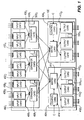
- FIGURE 1 depicts a block schematic of a broadcast router 100 in accordance with a preferred example of the present principles.
- the router 100 comprises at least one, and preferably a plurality of input modules 402 1 , 402 2 ...402 x where x is an integer greater than zero, and at least one, and preferably, a plurality of output modules 404 1 ...404 y , where y is an integer.
- Each input module such as input module 402 1 , comprises at least one, and preferably a plurality of input cards 406 1 , 406 2 ...406 z where z is an integer greater than zero.
- Each input card has at least one, and preferably, a plurality of inputs for receiving signals for multiplexing into an output signal.
- An expansion card 408 within each input module such as module 402 1 , multiplexes the output signals from the input cards 406 1 -406 z into an output signal.
- Each second module such as second module 404 1 , has a matrix 410 card which de-multiplexes the input signals from one or more of the input modules for delivery to at least one, and preferably a plurality of output cards 412 1 , 412 2 ...412 p , where p is an integer greater than zero.
- Each output card delivers one or more output signals to one or more external devices (not shown).
- a control card 414 controls the matrix card 410 in response to an external control signal C to cause the matrix card to route its output signal among various of the output cards 412 1 -412 p . In this way, the matrix card 410 can effectuate routing based on the external control signal C.
- the router 100 of FIG. 1 has each of its input modules 402 1 , 402 2 ...402 x coupled to each of the output modules 404 1 , 402 2. ..404 y .
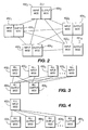
- FIGURE 2 illustrates a first alternate arrangement of input and output cards for the router 100 of FIG. 1 wherein the input and output modules are arranged to provide the same number of inputs and outputs.
- FIGURE 3 illustrates a second alternate arrangement of input and output modules for the router 100 of FIG. 1 in which there are more inputs than outputs.
- FIGURE 4 illustrates a third alternate arrangement of input and output modules for the router 100 of FIG. 1 in which there are more outputs than inputs.
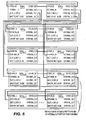
- the input modules 402 1 -402 x and the output modules 404 1 -404 y of FIG. 1 typically each include at least one of clock modules 500 1 -500 n where n ⁇ x + y , with each clock module having a structure as described in greater detail with respect to FIG. 5 .
- each clock module can exist in within one or more the elements within each input and output module of FIG. 1 .
- one or more clock modules 500 1 -500 n could exist as separate modular elements in the router 100, much like one of the input or output modules.
- the clock modules 500 1 -500 n can interconnect with each other in a daisy chain fashion to yield a network 600 of clock modules.
- the clock module 500 1 supplies its clock signal to the clock module 500 2 as well as each of clock modules 500 3 , 500 i + 1 and 500 i + 3 , where i ⁇ n
- the clock module 500 2 supplies its clock signal to each of modules 500 i , 500 i+2 and 500 i+4 .
- Each of the clock modules 500 1 , 500 2 ...500 n also receives the clock signal from a preceding one of clock modules 500 2 ...500 i ...500 n-1 , respectively.
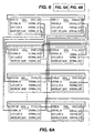
- FIGURE 6 depicts an alternate arrangement of clock modules wherein the modules are arranged in first and second networks 600 1 and 600 2 , with each of the networks 600 1 and 600 2 configured similarly to the clock module network 600 of FIG. 2 .
- one or more of the individual clock modules 500 1 -500 n of network 600 1 provide clock signals to one or more of the clock modules 500 1 -500 n of network 600 2 .
- FIGURE 7 depicts a block schematic diagram of an exemplary clock module 500 i .
- the clock module 500 i of FIG. 4 includes first and second clock inputs that receive first and second clock signals Clock_1 and Clock_2, respectively.
- Each of the external clock signals Clock_1 and Clock_2 can comprise clock signals from a separate upstream clock selector circuit in the network of FIG 2 or a clock signal from a reference clock circuit formed by an oscillator 508.
- the clock selector circuit 500 i includes a pair of toggle detectors 502 and 504 which each receive a separate one of the Clock_1 and Clock_2 signals. Each toggle detector provides an output signal indicative of whether its respective input clock signal has toggled, i.e., a changed from one state to another.
- a logic block 506 receives the output signals of the toggle detectors 502 and 504, along with the output of an oscillator circuit 508 that generates a clock signal useful for meeting the timing requirements of various circuit elements.
- the logic block 506 also receives two external status signals; (1) A_not B and (2) Master_not Slave.
- the state of the status signal A_not B indicates whether or not the clock circuit 500 i will provide the primary clock signal.
- the state of the Master_not Slave signal determines whether the clock circuit 500 i operates as its own master, or as a slave to another clock signal.
- the logic block 506 generates an output control for controlling a safe clock multiplexer system 510 to select among the clock signals Clock_1, Clock_2 and the output signal of the oscillator 508, to provide a single clock signal to downstream elements (not shown).
- the output control signal of the logic block 506 has a prescribed relationship to the logic circuit input signals as shown in Table 1, with the "x" entries constituting "don't care” values.
- the clock circuit 500 i only selects between Clock_2 and Oscillator 508. Under such conditions, the toggling of the Clock_1 signal, and hence the output signal of the toggle detector 504 has no effect. Conversely, when the clock circuit 500 i serves as a slave (i.e., the Master_ Not Slave signal remains at a logic "0" level), the output states of the toggle detector 504, and the output state of the toggle detector 502, determine which of the Clock_1, Clock_2, and oscillator 508 signals appear at the output of the safe clock multiplexer system 510.
- the clock signal selected by the safe clock multiplexer system 510 provides a timing signal for local use as well as for input to elements within the router 100 of FIG. 1 .
- the safe clock multiplexer system 510 of FIG. 4 has the structure shown in FIG. 5 to afford the clock module 500 i of FIG. 3 the ability to tolerate an input clock pulse that has become stuck.
- first and second toggle detectors 701 1 and 701 2 receive the Clock_1 and Clock_2 signals, respectively, as do each of a pair of multiplexers 702 1 and 702 2 , respectively.
- Each of the multiplexers 702 1 and 702 2 receives a signal and a logic "0" level at its second input.
- the toggle detectors 701 1 and 701 2 control the multiplexers 702 1 and 702 1 in accordance with the state of Clock_1 and Clock_2 signals, respectively, as measured against the output signal of the oscillator 508. In other words, each of the toggle detectors 701 1 and 701 2 determines whether a respective one of the Clock_1 and Clock_2 signals has changed state (i.e., toggled) relative to the output signal of the oscillator 508. If a respective one of the toggle detectors 701 1 and 701 2 determines that a corresponding one of the Clock_1 and Clock_2 signals has toggled relative to the oscillator 508 output signal, then that toggle detector gates a corresponding one of the multiplexers 702 1 and 702 2 .
- each of the multiplexers 702 1 and 702 2 passes an associated one of the Clock_1 and Clock_2 signals. Should a respective one of the clock signals Clock_1 and Clock_2 not toggle relative to the oscillator 508 output signal, then the corresponding one of the multiplexers 702 1 and 702 2 will output a logic zero level signal.
- a multiplexer 704 receives at its first and second inputs the output signals of the multiplexers 702 1 and 702 2 , respectively. In accordance with a signal from the logic block 506 of FIG. 4 , the multiplexer passes the output signal of one of the multiplexers 702 1 and 702 2 to a first input of a multiplexer 706 1 and to the input of a toggle detector 708 1 .
- the multiplexer 706 1 has its second input supplied with a signal at a logic zero level.
- the toggle detector 708 1 controls the multiplexer 706 1 in accordance with the relationship between the output signal of the multiplexer 704 and the output signal of the oscillator 508. In other words, the toggle detector 708 1 determines whether the output signal of the multiplexer 704 has changed state relative to the output signal of the oscillator 508. If the output signal of the multiplexer 704 toggles relative to the oscillator 508 output signal, then the toggle detector 708 1 causes the multiplexers 706 1 to pass the output signal of the multiplexer 704. Otherwise, should the output signal of the multiplexer 704 not toggle relative to the output signal of the oscillator 508, the multiplexer 706 1 will output a logic zero level signal.
- a multiplexer 706 2 receives at its first and second inputs the output signal of the oscillator 508 and a logic zero level signal, respectively.
- a toggle detector 708 2 controls the multiplexer 706 2 in accordance with the oscillator 508 output signal. In other words, the toggle detector 708 2 determines whether the output signal of the oscillator 508 periodically changes state. If the oscillator 508 output signal does toggle, then the toggle detector 708 2 gates the multiplexer 706 2 to pass the output signal of the oscillator 508. Otherwise, should the output signal of the oscillator 508 not toggle, then the multiplexer 706 2 will output a logic zero level signal.
- a multiplexer 710 receives at its first and second inputs the output signals of the multiplexers 706 1 and 706 2 , respectively. Like the multiplexer 704, the multiplexer 710 operates under the control of the logic block 506 of FIG. 4 . Thus, depending on output signal of the logic block 506, the multiplexer 710 will either output a selected one of the Clock_1 and Clock_2 signals (assuming at least one has toggled relative to the oscillator 508 output signal) or the output signal of the oscillator 508 (assuming it has toggled.)
- the multiplexers 702 1 and 702 2 and the multiplexers 704 and 710 serve as clock multiplexers as described earlier.
- the safe clock multiplexer system 510 of FIG. 5 precludes the possibility of a missing clock pulse.
- a clock selector circuit 500 i including a safe multiplexer system 510, for distributing clock pulses so as to provide for redundancy while assuring clock synchronism.
Abstract
Description
- This invention relates to routers and more specifically to broadcast routers that route asynchronous signals.
- A router comprises a device that routes one or more signals appearing at the router input(s) to one or more outputs. Routers used in the broadcast industry typically employ at least a first router portion with a plurality of router modules (also referred to as matrix cards) coupled to at least one expansion module. The expansion module couples the first router chassis to one or more second router portion to allow further routing of signals. Many broadcast routers, and especially those that are linearly expandable, route asynchronous signals. Asynchronous signal routing by such linearly expandable routers requires an accurate clock signal throughout the entire route to preserve the integrity of routed data. For an asynchronous signal, a difference in clock frequency from one location to another can cause corruption of the signal and loss of the data represented by that signal. Even a difference in clock frequencies as small as 1 part per million (PPM) can have an undesirable effect on data. Typical examples of data corruption include repeated or dropped signal samples.
- As linearly expandable routers increase in complexity, the problem of supplying an accurate and synchronized clock signal to various elements becomes more difficult. For purposes of discussion, a clock signal constitutes a signal that oscillates between a high and a low state at defined intervals. Typical clock signals oscillate with a 50% duty cycle. However, clocks having other duty cycles are also commonly employed. Circuits using clock signals for synchronization become active upon one of the rising or falling edge of the clock signal.
- A so-called, "clock multiplexer" refers to a circuit, as typically exists within a linearly expandable router, for selecting at least one clock signal from a plurality of available clock signals. The selected clock signal(s) serve to trigger other elements. When selecting among available clock signals, the output signal selected by the clock multiplexer should not include any undefined pluses. Undefined pulses occur, for example, when a selected clock signal undergoes a disruption. Such a disruption can include a missing clock signal as well as a clock signal that fails to switch states as expected. Some times, an input clock signal will remain "stuck" indefinitely at one logic state or the other. Such disruptions frequently produce undefined pulses including runt pulses, short pulses, pulses of indefinite duration, glitches, spikes and the like.
-
WO 2004/002089 discloses a router comprising a clock selector (506) for selecting from among first and second clock signals based in part on whether at least one of the first and second clock signals has toggled. If both clock signals fail, no clock can be selected, and the router fails completely. -
US 4 794 596 discloses a synchronized data network in which a clock selector is adapted to select between a plurality of master clocks, and in case of failure of these, a local auxiliary clock. -
US4322580 (Khan et al.; published on 30. March 1982 ) discloses a clock multiplexer with selection out of plural input clock signals. The selection is controlled by monitoring the toggling of each on the input clock signals. Input clock lines of which the signals do not toggle, e.g. due to a failure, are fixed to ground zero level. Toggling is monitored by a monostable multivibrator MV. MV is dimensioned to provide the logic zero as soon as 2 clock pulses are missing. - Prior art attempts to avid undefined pulses at the output of a clock multiplexer include so-called "safe" clock multiplexers. A typical safe clock multiplexer switches from a presently selected input to a next selected input in an orderly manner. Thus, a safe multiplexer does not switch until the selected input clock signal transitions to a known state and the subsequently selected clock signal transitions to the same state as the previously selected clock signal.
- However, prior art safe clock multiplexers have drawbacks. For example, when a presently selected clock signal fails to transition to a known state, a safe clock multiplexer will often lack the ability to switch to another clock signal. Prior art safe clock multiplexers have not tolerated these and other types of clock disruptions.
- Thus, a need exists for a technique for providing a selected one of a set of clock signals, such as within a linearly expandable router, that overcomes the aforementioned disadvantages
- Briefly in accordance with a preferred embodiment of the present principles, there is provided a method for selecting a clock signal from among at least first and second clock signals. The method commences by detecting a failure of a first clock signal to change state and by detecting a failure of a second clock signal to change state. A selection occurs from among the first and second clock signals and an oscillator signal, based in part on whether at least one of the first and second clock signals has toggled
-
FIGURE 1 illustrates a block schematic diagram of a router according to an illustrative example of the present principles: -
FIGURE 2 illustrates a first alternate arrangement of input and output modules for the router ofFIG. 1 -
FIGURE 3 illustrates a second alternate arrangement of input and output modules for the router ofFIG. 1 ; -
FIGURE 4 illustrates a third alternate arrangement of input and output modules for the router ofFIG. 1 -
FIGURE 5 illustrates a first network of clock selector circuits for use in the router ofFIG. 1 ; -
FIGURE 6 depicts a second network of clock selector circuits for use in the router ofFIG. 1 -
FIGURE 7 depicts a block schematic diagram of an illustrative embodiment of a clock selector circuit within the networks ofFIGS. 5 and6 ; and -
FIGURE 8 depicts a safe clock multiplexer system of for use in the selector circuit ofFIG. 4 . -
FIGURE 1 depicts a block schematic of abroadcast router 100 in accordance with a preferred example of the present principles. In a preferred example, therouter 100 comprises at least one, and preferably a plurality of input modules 4021, 4022...402x where x is an integer greater than zero, and at least one, and preferably, a plurality of output modules 4041...404y, where y is an integer. Each input module, such as input module 4021, comprises at least one, and preferably a plurality of input cards 4061, 4062...406z where z is an integer greater than zero. Each input card has at least one, and preferably, a plurality of inputs for receiving signals for multiplexing into an output signal. Different input cards typically have different signal receiving capabilities to afford the ability to receive signals from a variety of sources. An expansion card 408 within each input module, such as module 4021, multiplexes the output signals from the input cards 4061-406z into an output signal. - Each second module, such as second module 4041, has a
matrix 410 card which de-multiplexes the input signals from one or more of the input modules for delivery to at least one, and preferably a plurality of output cards 4121, 4122...412 p , where p is an integer greater than zero. Each output card delivers one or more output signals to one or more external devices (not shown). Acontrol card 414 controls thematrix card 410 in response to an external control signal C to cause the matrix card to route its output signal among various of the output cards 4121-412 p . In this way, thematrix card 410 can effectuate routing based on the external control signal C. - The
router 100 ofFIG. 1 has each of its input modules 4021, 4022...402x coupled to each of the output modules 4041, 4022...404y. Other arrangements are possible.FIGURE 2 illustrates a first alternate arrangement of input and output cards for therouter 100 ofFIG. 1 wherein the input and output modules are arranged to provide the same number of inputs and outputs.FIGURE 3 illustrates a second alternate arrangement of input and output modules for therouter 100 ofFIG. 1 in which there are more inputs than outputs.FIGURE 4 illustrates a third alternate arrangement of input and output modules for therouter 100 ofFIG. 1 in which there are more outputs than inputs. - The input modules 4021-402x and the output modules 4041-404y of
FIG. 1 typically each include at least one of clock modules 5001-500n where n ≥ x + y, with each clock module having a structure as described in greater detail with respect toFIG. 5 . In practice, separate clock modules can exist in within one or more the elements within each input and output module ofFIG. 1 . Moreover, one or more clock modules 5001-500n could exist as separate modular elements in therouter 100, much like one of the input or output modules. - Referring to
FIG. 5 , the clock modules 5001-500n can interconnect with each other in a daisy chain fashion to yield a network 600 of clock modules. In the embodiment ofFIG. 5 , theclock module 5001 supplies its clock signal to theclock module 5002 as well as each ofclock modules clock module 5002 supplies its clock signal to each ofmodules clock modules clock modules 5002...500 i ...500 n-1 , respectively. -
FIGURE 6 depicts an alternate arrangement of clock modules wherein the modules are arranged in first and second networks 6001 and 6002, with each of the networks 6001 and 6002 configured similarly to the clock module network 600 ofFIG. 2 . As seen inFIG. 6 , one or more of the individual clock modules 5001-500n of network 6001 provide clock signals to one or more of the clock modules 5001-500n of network 6002. -
FIGURE 7 depicts a block schematic diagram of anexemplary clock module 500 i . Theclock module 500 i ofFIG. 4 includes first and second clock inputs that receive first and second clock signals Clock_1 and Clock_2, respectively. Each of the external clock signals Clock_1 and Clock_2 can comprise clock signals from a separate upstream clock selector circuit in the network ofFIG 2 or a clock signal from a reference clock circuit formed by anoscillator 508. - The
clock selector circuit 500 i includes a pair oftoggle detectors logic block 506 receives the output signals of thetoggle detectors oscillator circuit 508 that generates a clock signal useful for meeting the timing requirements of various circuit elements. Thelogic block 506 also receives two external status signals; (1) A_not B and (2) Master_not Slave. The state of the status signal A_not B indicates whether or not theclock circuit 500 i will provide the primary clock signal. The state of the Master_not Slave signal determines whether theclock circuit 500 i operates as its own master, or as a slave to another clock signal. - The
logic block 506 generates an output control for controlling a safeclock multiplexer system 510 to select among the clock signals Clock_1, Clock_2 and the output signal of theoscillator 508, to provide a single clock signal to downstream elements (not shown). The output control signal of thelogic block 506 has a prescribed relationship to the logic circuit input signals as shown in Table 1, with the "x" entries constituting "don't care" values. (In other words, the value of the particular input signal has no effect on the output of thelogic block 506.)TABLE I A_not B Master_Not Slave Toggle Detector 504 Toggle Detector 502Safe clock multiplexer system 510Output 1 1 x x Oscillator 5080 1 x 1 Clock_2 0 1 x 0 Oscillator 508 x 0 1 x Clock_1 x 0 0 1 Clock_2 x 0 0 0 Oscillator 508 - As seen from Table 1, for so long as the Master_ Not Slave signal remains at a logic "1" level, the
clock circuit 500 i only selects between Clock_2 andOscillator 508. Under such conditions, the toggling of the Clock_1 signal, and hence the output signal of thetoggle detector 504 has no effect. Conversely, when theclock circuit 500 i serves as a slave (i.e., the Master_ Not Slave signal remains at a logic "0" level), the output states of thetoggle detector 504, and the output state of thetoggle detector 502, determine which of the Clock_1, Clock_2, andoscillator 508 signals appear at the output of the safeclock multiplexer system 510. The clock signal selected by the safeclock multiplexer system 510 provides a timing signal for local use as well as for input to elements within therouter 100 ofFIG. 1 . - In a preferred embodiment, the safe
clock multiplexer system 510 ofFIG. 4 has the structure shown inFIG. 5 to afford theclock module 500 i ofFIG. 3 the ability to tolerate an input clock pulse that has become stuck. Within the safeclock multiplexer system 510 ofFIG. 5 , first and second toggle detectors 7011 and 7012 receive the Clock_1 and Clock_2 signals, respectively, as do each of a pair of multiplexers 7021 and 7022, respectively. Each of the multiplexers 7021 and 7022 receives a signal and a logic "0" level at its second input. - The toggle detectors 7011 and 7012 control the multiplexers 7021 and 7021 in accordance with the state of Clock_1 and Clock_2 signals, respectively, as measured against the output signal of the
oscillator 508. In other words, each of the toggle detectors 7011 and 7012 determines whether a respective one of the Clock_1 and Clock_2 signals has changed state (i.e., toggled) relative to the output signal of theoscillator 508. If a respective one of the toggle detectors 7011 and 7012 determines that a corresponding one of the Clock_1 and Clock_2 signals has toggled relative to theoscillator 508 output signal, then that toggle detector gates a corresponding one of the multiplexers 7021 and 7022. When gated, each of the multiplexers 7021 and 7022 passes an associated one of the Clock_1 and Clock_2 signals. Should a respective one of the clock signals Clock_1 and Clock_2 not toggle relative to theoscillator 508 output signal, then the corresponding one of the multiplexers 7021 and 7022 will output a logic zero level signal. - A
multiplexer 704 receives at its first and second inputs the output signals of the multiplexers 7021 and 7022, respectively. In accordance with a signal from thelogic block 506 ofFIG. 4 , the multiplexer passes the output signal of one of the multiplexers 7021 and 7022 to a first input of a multiplexer 7061 and to the input of a toggle detector 7081. The multiplexer 7061 has its second input supplied with a signal at a logic zero level. - The toggle detector 7081 controls the multiplexer 7061 in accordance with the relationship between the output signal of the
multiplexer 704 and the output signal of theoscillator 508. In other words, the toggle detector 7081 determines whether the output signal of themultiplexer 704 has changed state relative to the output signal of theoscillator 508. If the output signal of themultiplexer 704 toggles relative to theoscillator 508 output signal, then the toggle detector 7081 causes the multiplexers 7061 to pass the output signal of themultiplexer 704. Otherwise, should the output signal of themultiplexer 704 not toggle relative to the output signal of theoscillator 508, the multiplexer 7061 will output a logic zero level signal. - A multiplexer 7062 receives at its first and second inputs the output signal of the
oscillator 508 and a logic zero level signal, respectively. A toggle detector 7082 controls the multiplexer 7062 in accordance with theoscillator 508 output signal. In other words, the toggle detector 7082 determines whether the output signal of theoscillator 508 periodically changes state. If theoscillator 508 output signal does toggle, then the toggle detector 7082 gates the multiplexer 7062 to pass the output signal of theoscillator 508. Otherwise, should the output signal of theoscillator 508 not toggle, then the multiplexer 7062 will output a logic zero level signal. - A
multiplexer 710 receives at its first and second inputs the output signals of the multiplexers 7061 and 7062, respectively. Like themultiplexer 704, themultiplexer 710 operates under the control of thelogic block 506 ofFIG. 4 . Thus, depending on output signal of thelogic block 506, themultiplexer 710 will either output a selected one of the Clock_1 and Clock_2 signals (assuming at least one has toggled relative to theoscillator 508 output signal) or the output signal of the oscillator 508 (assuming it has toggled.) - An important distinction exists between the multiplexers 7021 and 7022 and the
multiplexers multiplexers clock multiplexer system 510 ofFIG. 5 precludes the possibility of a missing clock pulse. By controlling the passage of the Clock_1 and Clock_2 signals relative to theoscillator 508 output signal and by controlling the passage of theoscillator 508 output only if it has toggled, the safeclock multiplexer system 510 avoids a situation in which any or all of the clocks become stuck in a no-clock state. - The foregoing describes a
clock selector circuit 500 i , including asafe multiplexer system 510, for distributing clock pulses so as to provide for redundancy while assuring clock synchronism.
Claims (10)
- Apparatus comprising:a clock selector (506) for selecting from among first and second clock signals (Clock_1, Clock_2), and an oscillator (508) signal, as a common output clock signal, based on whether at least one of the first and second clock signals (Clock_1, Clock_2) has toggled,a safe clock multiplexer system (502, 504, 510) for detecting whether each of the first and second clock signals (Clock_1, Clock_2) has toggled compared to the oscillator (508) signal, and if not replacing said each non-toggling clock signal (Clock_1, Clock_2) with a signal at the same fixed logic state.
- The apparatus according to claim 1 wherein the safe clock multiplexer circuit (502, 504, 510) includes a pair of toggle detectors (502, 504), each determining whether a separate one of the first and second clock signals (Clock_1, Clock_2) has toggled compared to the oscillator (508) signal.
- The apparatus according to claim 1 wherein the clock selector circuit (506) selects from among said first and second clock signal (Clock_1, Clock_2), and the oscillator (508) signal, as a common output clock signal, based in part on whether at least one of the first and second clock signals (Clock_1, Clock_2) has toggled and whether the clock selector circuit (506) serves as a master or as a slave to another clock selector circuit.
- The apparatus according to claim 1 wherein the clock selector circuit (506) selects from among said first and second clock signal (Clock_1, Clock_2), and the oscillator (508) output signal, as a common output clock signal, based in part on:i) whether at least one of the first and second clock signals (Clock_1, Clock_2) has toggled,ii) whether the clock serves as its own master, or as a slave to another clock selector circuit, and
- The apparatus according to claim 1 wherein the clock selector circuit comprises:a first toggle detector (502) for generating an output signal determinative of whether the first external clock signal (Clock_1) has toggled;a second toggle detector (504) for generating an output signal determinative of whether the second external clock signal (Clock_2) has toggled;a logic block (506) for providing an output control signal which varies based in part on the output signal of the first and second toggle detectors (502, 504); anda multiplexer system (510) for selecting among said first and second clock signal (Clock_1, Clock_2), and said oscillator (508) signal, as a common output clock signal for the at least first router in accordance with the logic block (506) output signal.
- The apparatus according to claim 5 wherein the logic block (506) provides its output control signal based in part on whether at least one of the first and second clock signals (Clock_1, Clock_2) has toggled, and whether the clock serves as its own master, or as a slave to another clock selector circuit.
- The apparatus according to claim 5 wherein the logic block (506) provides its output control signal based in part on:i) whether at least one of the first and second clock signals (Clock_1, Clock_2) has toggled,ii) whether the clock serves as its own master, or as a slave to another clock selector circuit, andiii) whether the common output clock signal will serve as a primary clock signal.
- The apparatus according to claim 1 further comprising:a second clock selector for selecting from among said first and second clock signals, and an oscillator signal, as a common output clock signal, based in part on whether at least one of the first and second clock signals has toggled compared to the oscillator signal.
- A method for selecting a clock signal, comprising the steps of
detecting a failure of a first clock signal (Clock_1) to toggle
detecting a failure of a second clock signal (Clock_2) to toggle; and
selecting from among the first and second clock signals (Clock_1, Clock_2) and an oscillator (508) signal, based on whether at least one of the first and second clock signals (Clock_1, Clock_2) has toggled compared to the oscillator (508) signal and
if one of the first and second clock signals (Clock_1, Clock_2) has not toggled, then replacing each non-toggling clock signal with a signal at the same fixed logic state. - The method according to claim 9 wherein the selecting step further comprises selecting from among said first and second clock signal (Clock_1, Clock_2), and an oscillator (508) signal, as a common output clock signal, based in part on whether the clock serves as its own master or as a slave to another clock selector circuit.
Applications Claiming Priority (3)
| Application Number | Priority Date | Filing Date | Title |
|---|---|---|---|
| US58018904P | 2004-06-16 | 2004-06-16 | |
| US58018804P | 2004-06-16 | 2004-06-16 | |
| PCT/US2005/019115 WO2006009605A1 (en) | 2004-06-16 | 2005-06-01 | System and method for routing asynchronous signals |
Publications (2)
| Publication Number | Publication Date |
|---|---|
| EP1756988A1 EP1756988A1 (en) | 2007-02-28 |
| EP1756988B1 true EP1756988B1 (en) | 2011-01-05 |
Family
ID=34972785
Family Applications (1)
| Application Number | Title | Priority Date | Filing Date |
|---|---|---|---|
| EP05762318A Expired - Fee Related EP1756988B1 (en) | 2004-06-16 | 2005-06-01 | System and method for routing asynchronous signals |
Country Status (7)
| Country | Link |
|---|---|
| EP (1) | EP1756988B1 (en) |
| JP (1) | JP4650956B2 (en) |
| KR (1) | KR101095832B1 (en) |
| CN (1) | CN101095300B (en) |
| CA (1) | CA2569018C (en) |
| DE (1) | DE602005025761D1 (en) |
| WO (1) | WO2006009605A1 (en) |
Families Citing this family (1)
| Publication number | Priority date | Publication date | Assignee | Title |
|---|---|---|---|---|
| CN105376042B (en) * | 2015-10-27 | 2019-04-02 | 国家电网公司 | A kind of ZH-550 clock synchronization system |
Citations (3)
| Publication number | Priority date | Publication date | Assignee | Title |
|---|---|---|---|---|
| US4794596A (en) * | 1985-07-01 | 1988-12-27 | Gloyne Francis R | Data network synchronisation |
| EP0530393A1 (en) * | 1991-09-02 | 1993-03-10 | Siemens Aktiengesellschaft | Method and apparatus for synchronising a clockcircuit of a switching communication system |
| US6121816A (en) * | 1999-04-23 | 2000-09-19 | Semtech Corporation | Slave clock generation system and method for synchronous telecommunications networks |
Family Cites Families (6)
| Publication number | Priority date | Publication date | Assignee | Title |
|---|---|---|---|---|
| US4322580A (en) * | 1980-09-02 | 1982-03-30 | Gte Automatic Electric Labs Inc. | Clock selection circuit |
| US5479648A (en) * | 1994-08-30 | 1995-12-26 | Stratus Computer, Inc. | Method and apparatus for switching clock signals in a fault-tolerant computer system |
| US6658580B1 (en) * | 2000-05-20 | 2003-12-02 | Equipe Communications Corporation | Redundant, synchronous central timing systems with constant master voltage controls and variable slave voltage controls |
| US7023442B2 (en) * | 2000-06-28 | 2006-04-04 | Sun Microsystems, Inc. | Transferring a digital video stream through a series of hardware modules |
| US6999546B2 (en) * | 2000-12-29 | 2006-02-14 | Nokia, Inc. | System and method for timing references for line interfaces |
| WO2004002089A1 (en) * | 2002-06-21 | 2003-12-31 | Thomson Licensing S.A. | A multi-chassis broadcast router having a common clock |
-
2005
- 2005-06-01 CA CA2569018A patent/CA2569018C/en not_active Expired - Fee Related
- 2005-06-01 DE DE602005025761T patent/DE602005025761D1/en active Active
- 2005-06-01 WO PCT/US2005/019115 patent/WO2006009605A1/en not_active Application Discontinuation
- 2005-06-01 EP EP05762318A patent/EP1756988B1/en not_active Expired - Fee Related
- 2005-06-01 CN CN2005800196590A patent/CN101095300B/en not_active Expired - Fee Related
- 2005-06-01 KR KR1020067026532A patent/KR101095832B1/en not_active IP Right Cessation
- 2005-06-01 JP JP2007516524A patent/JP4650956B2/en not_active Expired - Fee Related
Patent Citations (3)
| Publication number | Priority date | Publication date | Assignee | Title |
|---|---|---|---|---|
| US4794596A (en) * | 1985-07-01 | 1988-12-27 | Gloyne Francis R | Data network synchronisation |
| EP0530393A1 (en) * | 1991-09-02 | 1993-03-10 | Siemens Aktiengesellschaft | Method and apparatus for synchronising a clockcircuit of a switching communication system |
| US6121816A (en) * | 1999-04-23 | 2000-09-19 | Semtech Corporation | Slave clock generation system and method for synchronous telecommunications networks |
Also Published As
| Publication number | Publication date |
|---|---|
| CA2569018A1 (en) | 2006-01-26 |
| DE602005025761D1 (en) | 2011-02-17 |
| CN101095300A (en) | 2007-12-26 |
| KR20070022756A (en) | 2007-02-27 |
| CA2569018C (en) | 2013-12-10 |
| EP1756988A1 (en) | 2007-02-28 |
| KR101095832B1 (en) | 2011-12-16 |
| JP4650956B2 (en) | 2011-03-16 |
| WO2006009605A1 (en) | 2006-01-26 |
| CN101095300B (en) | 2012-05-16 |
| JP2008503917A (en) | 2008-02-07 |
Similar Documents
| Publication | Publication Date | Title |
|---|---|---|
| EP1097511B1 (en) | Slave clock generation system and method for synchronous telecommunications networks | |
| KR100598476B1 (en) | Apparatus/method for distributing a clock signal | |
| US7627003B1 (en) | Automatic clock synchronization and distribution circuit for counter clock flow pipelined systems | |
| US6895189B1 (en) | Optical synchronization system | |
| EP2871550B1 (en) | Clocking for pipelined routing | |
| US7308592B2 (en) | Redundant oscillator distribution in a multi-processor server system | |
| EP0841834B1 (en) | Method and apparatus for a hitless switch-over between redundant signals | |
| US6832347B1 (en) | Clock synchronization and fault protection for a telecommunications device | |
| KR100871205B1 (en) | System for Concluding Phase of Multi-Clock | |
| EP3938862A1 (en) | Clock distribution resonator system | |
| US5381416A (en) | Detection of skew fault in a multiple clock system | |
| US5666079A (en) | Binary relative delay line | |
| US7656215B2 (en) | Clock generator circuit, clock selector circuit, and semiconductor integrated circuit | |
| EP1756988B1 (en) | System and method for routing asynchronous signals | |
| US8116321B2 (en) | System and method for routing asynchronous signals | |
| US5327402A (en) | Clock supply apparatus | |
| US7721133B2 (en) | Systems and methods of synchronizing reference frequencies | |
| US7350116B1 (en) | Clock synchronization and fault protection for a telecommunications device | |
| US4975594A (en) | Frequency detector circuit | |
| JPH0897750A (en) | Clock reception distribution system | |
| US20110050297A1 (en) | System employing synchronized crystal oscillator-based clock | |
| KR100280210B1 (en) | Clock generation / distribution apparatus and method in ATM switching system | |
| US7468991B2 (en) | Methods and devices for synchronizing the timing of logic cards in a packet switching system without data loss | |
| JP4192581B2 (en) | Clock switching device | |
| JPH06261028A (en) | Clock distribution system for synchronization communications equipment |
Legal Events
| Date | Code | Title | Description |
|---|---|---|---|
| PUAI | Public reference made under article 153(3) epc to a published international application that has entered the european phase |
Free format text: ORIGINAL CODE: 0009012 |
|
| 17P | Request for examination filed |
Effective date: 20061212 |
|
| AK | Designated contracting states |
Kind code of ref document: A1 Designated state(s): DE FR GB |
|
| DAX | Request for extension of the european patent (deleted) | ||
| RBV | Designated contracting states (corrected) |
Designated state(s): DE FR GB |
|
| 17Q | First examination report despatched |
Effective date: 20071023 |
|
| RAP1 | Party data changed (applicant data changed or rights of an application transferred) |
Owner name: THOMSON LICENSING |
|
| GRAP | Despatch of communication of intention to grant a patent |
Free format text: ORIGINAL CODE: EPIDOSNIGR1 |
|
| GRAS | Grant fee paid |
Free format text: ORIGINAL CODE: EPIDOSNIGR3 |
|
| GRAA | (expected) grant |
Free format text: ORIGINAL CODE: 0009210 |
|
| AK | Designated contracting states |
Kind code of ref document: B1 Designated state(s): DE FR GB |
|
| REG | Reference to a national code |
Ref country code: GB Ref legal event code: FG4D |
|
| REF | Corresponds to: |
Ref document number: 602005025761 Country of ref document: DE Date of ref document: 20110217 Kind code of ref document: P |
|
| REG | Reference to a national code |
Ref country code: DE Ref legal event code: R096 Ref document number: 602005025761 Country of ref document: DE Effective date: 20110217 |
|
| REG | Reference to a national code |
Ref country code: DE Ref legal event code: R084 Ref document number: 602005025761 Country of ref document: DE |
|
| REG | Reference to a national code |
Ref country code: GB Ref legal event code: 746 Effective date: 20110309 |
|
| PLBE | No opposition filed within time limit |
Free format text: ORIGINAL CODE: 0009261 |
|
| STAA | Information on the status of an ep patent application or granted ep patent |
Free format text: STATUS: NO OPPOSITION FILED WITHIN TIME LIMIT |
|
| 26N | No opposition filed |
Effective date: 20111006 |
|
| REG | Reference to a national code |
Ref country code: DE Ref legal event code: R097 Ref document number: 602005025761 Country of ref document: DE Effective date: 20111006 |
|
| PGFP | Annual fee paid to national office [announced via postgrant information from national office to epo] |
Ref country code: DE Payment date: 20150625 Year of fee payment: 11 |
|
| REG | Reference to a national code |
Ref country code: FR Ref legal event code: PLFP Year of fee payment: 12 |
|
| REG | Reference to a national code |
Ref country code: DE Ref legal event code: R119 Ref document number: 602005025761 Country of ref document: DE |
|
| PG25 | Lapsed in a contracting state [announced via postgrant information from national office to epo] |
Ref country code: DE Free format text: LAPSE BECAUSE OF NON-PAYMENT OF DUE FEES Effective date: 20170103 |
|
| REG | Reference to a national code |
Ref country code: FR Ref legal event code: PLFP Year of fee payment: 13 |
|
| REG | Reference to a national code |
Ref country code: FR Ref legal event code: PLFP Year of fee payment: 14 |
|
| PGFP | Annual fee paid to national office [announced via postgrant information from national office to epo] |
Ref country code: FR Payment date: 20180620 Year of fee payment: 14 |
|
| PGFP | Annual fee paid to national office [announced via postgrant information from national office to epo] |
Ref country code: GB Payment date: 20180627 Year of fee payment: 14 |
|
| GBPC | Gb: european patent ceased through non-payment of renewal fee |
Effective date: 20190601 |
|
| PG25 | Lapsed in a contracting state [announced via postgrant information from national office to epo] |
Ref country code: GB Free format text: LAPSE BECAUSE OF NON-PAYMENT OF DUE FEES Effective date: 20190601 |
|
| PG25 | Lapsed in a contracting state [announced via postgrant information from national office to epo] |
Ref country code: FR Free format text: LAPSE BECAUSE OF NON-PAYMENT OF DUE FEES Effective date: 20190630 |
|
| P01 | Opt-out of the competence of the unified patent court (upc) registered |
Effective date: 20230621 |