EP1756876B1 - High density led array - Google Patents
High density led array Download PDFInfo
- Publication number
- EP1756876B1 EP1756876B1 EP05734339A EP05734339A EP1756876B1 EP 1756876 B1 EP1756876 B1 EP 1756876B1 EP 05734339 A EP05734339 A EP 05734339A EP 05734339 A EP05734339 A EP 05734339A EP 1756876 B1 EP1756876 B1 EP 1756876B1
- Authority
- EP
- European Patent Office
- Prior art keywords
- micro
- array
- reflector
- perimeter shape
- dense array
- Prior art date
- Legal status (The legal status is an assumption and is not a legal conclusion. Google has not performed a legal analysis and makes no representation as to the accuracy of the status listed.)
- Active
Links
- 238000012856 packing Methods 0.000 claims abstract description 61
- 239000004065 semiconductor Substances 0.000 claims abstract description 42
- 230000007704 transition Effects 0.000 claims description 30
- 230000008878 coupling Effects 0.000 claims description 16
- 238000010168 coupling process Methods 0.000 claims description 16
- 238000005859 coupling reaction Methods 0.000 claims description 16
- 238000001228 spectrum Methods 0.000 claims description 8
- 239000002826 coolant Substances 0.000 claims description 6
- 238000001816 cooling Methods 0.000 description 23
- 238000013459 approach Methods 0.000 description 11
- ORQBXQOJMQIAOY-UHFFFAOYSA-N nobelium Chemical compound [No] ORQBXQOJMQIAOY-UHFFFAOYSA-N 0.000 description 11
- 239000000463 material Substances 0.000 description 10
- 239000000758 substrate Substances 0.000 description 10
- 238000003491 array Methods 0.000 description 6
- 238000000034 method Methods 0.000 description 6
- 238000012544 monitoring process Methods 0.000 description 6
- 230000008569 process Effects 0.000 description 6
- 238000005516 engineering process Methods 0.000 description 5
- 230000003287 optical effect Effects 0.000 description 5
- 230000005855 radiation Effects 0.000 description 5
- 238000007514 turning Methods 0.000 description 5
- 230000007423 decrease Effects 0.000 description 4
- 238000004519 manufacturing process Methods 0.000 description 4
- 230000000694 effects Effects 0.000 description 3
- 238000003754 machining Methods 0.000 description 3
- 230000013011 mating Effects 0.000 description 3
- 230000005540 biological transmission Effects 0.000 description 2
- 230000015556 catabolic process Effects 0.000 description 2
- 238000000576 coating method Methods 0.000 description 2
- 230000006378 damage Effects 0.000 description 2
- 238000006731 degradation reaction Methods 0.000 description 2
- 238000010586 diagram Methods 0.000 description 2
- 238000009826 distribution Methods 0.000 description 2
- 230000002708 enhancing effect Effects 0.000 description 2
- 238000005530 etching Methods 0.000 description 2
- 238000007726 management method Methods 0.000 description 2
- 239000002184 metal Substances 0.000 description 2
- 229910052751 metal Inorganic materials 0.000 description 2
- 238000012986 modification Methods 0.000 description 2
- 230000004048 modification Effects 0.000 description 2
- 238000007639 printing Methods 0.000 description 2
- 238000000926 separation method Methods 0.000 description 2
- 239000011800 void material Substances 0.000 description 2
- RYGMFSIKBFXOCR-UHFFFAOYSA-N Copper Chemical compound [Cu] RYGMFSIKBFXOCR-UHFFFAOYSA-N 0.000 description 1
- 230000003466 anti-cipated effect Effects 0.000 description 1
- 230000015572 biosynthetic process Effects 0.000 description 1
- 238000005266 casting Methods 0.000 description 1
- 230000008859 change Effects 0.000 description 1
- 239000012809 cooling fluid Substances 0.000 description 1
- 229910052802 copper Inorganic materials 0.000 description 1
- 239000010949 copper Substances 0.000 description 1
- 230000003467 diminishing effect Effects 0.000 description 1
- 238000005242 forging Methods 0.000 description 1
- 238000010438 heat treatment Methods 0.000 description 1
- 230000000977 initiatory effect Effects 0.000 description 1
- 239000007788 liquid Substances 0.000 description 1
- 238000001459 lithography Methods 0.000 description 1
- 239000011295 pitch Substances 0.000 description 1
- 230000009467 reduction Effects 0.000 description 1
- 230000003595 spectral effect Effects 0.000 description 1
- 238000012795 verification Methods 0.000 description 1
Images


Classifications
-
- F—MECHANICAL ENGINEERING; LIGHTING; HEATING; WEAPONS; BLASTING
- F21—LIGHTING
- F21K—NON-ELECTRIC LIGHT SOURCES USING LUMINESCENCE; LIGHT SOURCES USING ELECTROCHEMILUMINESCENCE; LIGHT SOURCES USING CHARGES OF COMBUSTIBLE MATERIAL; LIGHT SOURCES USING SEMICONDUCTOR DEVICES AS LIGHT-GENERATING ELEMENTS; LIGHT SOURCES NOT OTHERWISE PROVIDED FOR
- F21K9/00—Light sources using semiconductor devices as light-generating elements, e.g. using light-emitting diodes [LED] or lasers
-
- H—ELECTRICITY
- H01—ELECTRIC ELEMENTS
- H01L—SEMICONDUCTOR DEVICES NOT COVERED BY CLASS H10
- H01L25/00—Assemblies consisting of a plurality of individual semiconductor or other solid state devices ; Multistep manufacturing processes thereof
- H01L25/03—Assemblies consisting of a plurality of individual semiconductor or other solid state devices ; Multistep manufacturing processes thereof all the devices being of a type provided for in the same subgroup of groups H01L27/00 - H01L33/00, or in a single subclass of H10K, H10N, e.g. assemblies of rectifier diodes
- H01L25/04—Assemblies consisting of a plurality of individual semiconductor or other solid state devices ; Multistep manufacturing processes thereof all the devices being of a type provided for in the same subgroup of groups H01L27/00 - H01L33/00, or in a single subclass of H10K, H10N, e.g. assemblies of rectifier diodes the devices not having separate containers
- H01L25/075—Assemblies consisting of a plurality of individual semiconductor or other solid state devices ; Multistep manufacturing processes thereof all the devices being of a type provided for in the same subgroup of groups H01L27/00 - H01L33/00, or in a single subclass of H10K, H10N, e.g. assemblies of rectifier diodes the devices not having separate containers the devices being of a type provided for in group H01L33/00
- H01L25/0753—Assemblies consisting of a plurality of individual semiconductor or other solid state devices ; Multistep manufacturing processes thereof all the devices being of a type provided for in the same subgroup of groups H01L27/00 - H01L33/00, or in a single subclass of H10K, H10N, e.g. assemblies of rectifier diodes the devices not having separate containers the devices being of a type provided for in group H01L33/00 the devices being arranged next to each other
-
- H—ELECTRICITY
- H01—ELECTRIC ELEMENTS
- H01L—SEMICONDUCTOR DEVICES NOT COVERED BY CLASS H10
- H01L2924/00—Indexing scheme for arrangements or methods for connecting or disconnecting semiconductor or solid-state bodies as covered by H01L24/00
- H01L2924/0001—Technical content checked by a classifier
- H01L2924/0002—Not covered by any one of groups H01L24/00, H01L24/00 and H01L2224/00
-
- H—ELECTRICITY
- H01—ELECTRIC ELEMENTS
- H01L—SEMICONDUCTOR DEVICES NOT COVERED BY CLASS H10
- H01L33/00—Semiconductor devices with at least one potential-jump barrier or surface barrier specially adapted for light emission; Processes or apparatus specially adapted for the manufacture or treatment thereof or of parts thereof; Details thereof
- H01L33/48—Semiconductor devices with at least one potential-jump barrier or surface barrier specially adapted for light emission; Processes or apparatus specially adapted for the manufacture or treatment thereof or of parts thereof; Details thereof characterised by the semiconductor body packages
- H01L33/58—Optical field-shaping elements
- H01L33/60—Reflective elements
-
- H—ELECTRICITY
- H01—ELECTRIC ELEMENTS
- H01L—SEMICONDUCTOR DEVICES NOT COVERED BY CLASS H10
- H01L33/00—Semiconductor devices with at least one potential-jump barrier or surface barrier specially adapted for light emission; Processes or apparatus specially adapted for the manufacture or treatment thereof or of parts thereof; Details thereof
- H01L33/48—Semiconductor devices with at least one potential-jump barrier or surface barrier specially adapted for light emission; Processes or apparatus specially adapted for the manufacture or treatment thereof or of parts thereof; Details thereof characterised by the semiconductor body packages
- H01L33/64—Heat extraction or cooling elements
- H01L33/644—Heat extraction or cooling elements in intimate contact or integrated with parts of the device other than the semiconductor body
-
- H—ELECTRICITY
- H01—ELECTRIC ELEMENTS
- H01L—SEMICONDUCTOR DEVICES NOT COVERED BY CLASS H10
- H01L33/00—Semiconductor devices with at least one potential-jump barrier or surface barrier specially adapted for light emission; Processes or apparatus specially adapted for the manufacture or treatment thereof or of parts thereof; Details thereof
- H01L33/48—Semiconductor devices with at least one potential-jump barrier or surface barrier specially adapted for light emission; Processes or apparatus specially adapted for the manufacture or treatment thereof or of parts thereof; Details thereof characterised by the semiconductor body packages
- H01L33/64—Heat extraction or cooling elements
- H01L33/648—Heat extraction or cooling elements the elements comprising fluids, e.g. heat-pipes
Definitions
- This invention relates to high-density light emitting semiconductor device arrays and, more particularly, to a light emitting diode (LED) array having optical elements directed toward optimizing high-density packing of the LEDs in balance with collection and collimation of the LEDs' radiant output.
- LED light emitting diode
- Light-emitting semiconductor devices may be arranged in various configurations, such as arrays, for lighting applications. Examples of these applications include: lithographic processes used, e.g., in fabricating semiconductor devices, and curing processes used, e.g., for ink printing and fabrication of DVDs. These applications generally have associated parameters, including, e.g., a photoreaction may contemplate provision of one or more radiant power densities at the work surface, at one or more wavelengths, applied over one or more periods of time and within thermal limitations.
- the light emitting semiconductor devices generally are employed to deliver against the parameter.
- the light emitting semiconductor devices typically have certain operating characteristics and specifications.
- the characteristics include: total power emitted; power stability; radiance; radiant intensity; the wavelength(s) of the radiant output; the coherence of the radiant output; the collimation of the radiant output; as well as other operative functionalitles provided by the semiconductor device as a light system (e.g., ability to provide pulsed operation and/or effective thermal management).
- the light emitting semiconductor device's specifications generally are associated with its fabrication and, among other things, are directed to preclude destruction and/or forestall degradation of the devices. These specifications generally include operating temperatures and applied, electrical power.
- a LED array may have some difficulty in that delivery. That follows because a typical LED in an array has a widely distributed radiant output. Indeed, a typical LED mounted alone on a planar substrate will exhibit a radiant output distributed characteristically across the hemisphere centered at the LED. Given such distribution, only some portion, often relatively small, of that radiant output is directed toward the work surface, thus diminishing the radiant power density at or across the surface. Moreover, such distribution implicates that, as the work surface becomes more physically separated from the LED, the radiant power density at or across the work surface will decrease rapidly, i.e., the decrease generally is anticipated to be proportional to the square of the separation.
- a basic LED array may simply be disposed physically proximate the work surface.
- this approach generally is undesirable because, e.g., close proximity tends to necessitate undesirable changes to tooling and/or shielding.
- an array may locate conventional refractive lenses above the LEDs. This approach contemplates that each LED is associated with a conventional lens so that the lens collects and collimates the LED's radiant output.
- a LED is mounted in a reflector (e.g., having a parabolic form).
- reflective optics generally collect and collimate a substantial portion of the LED's radiant output.
- conventional reflective optics generally are not used in a tightly packed or dense array because of their size.
- a typical application of conventional reflective optics is illustrated by LED flashlights in which one or more LEDs are mounted in a large reflective optic, so that the optic collects light from such LEDs.
- An array of light emitting semiconductor devices in accordance with the invention is defined in claim 1 and includes optical elements selected toward optimizing high-density packing of the devices in the array in balance with collection and collimation of the devices' radiant output.
- an array of LEDs is coupled with a micro-reflector array, which micro-reflector array includes a plurality of micro-reflector elements.
- Each such micro-reflector element is a parabolic reflector, or otherwise has a basic volumetric form associated with a selected surface of revolution.
- Each such micro-reflector element has a lower portion and an upper portion.
- the upper portion is characterized by a packing edge having a selected perimeter shape.
- the perimeter shape if responsive to the volumetric form, will be a circle, because this shape is the outline of any cross-section taken at the upper portion of an element having a volumetric form associated with a surface of revolution. Because circles do not pack as densely as may be desired and because, when packed, circles leave gaps there between, in this example embodiment, each individual element's packing edge preferably has a perimeter shape other than that responsive to the volumetric form.
- the packing edge preferably has a perimeter shape selected so as to enhance mating with the packing edges of the micro-reflector elements adjacent such individual element in the array and, thereby, among other things, increase the packing density of the LED array.
- the packing edge typically is a selected polygon, such as a square or a hexagon.
- the micro-reflector array comprises more than one type of micro-reflector element, the pluralities of each such type of elements typically being arranged in a selected pattern thereamong.
- An example includes employing one micro-reflector element having a packing edge of one perimeter shape and another micro-reflector element having a packing edge of a second perimeter shape.
- various combinations of perimeter shapes may be used without deviating from the principles of the invention, including: (a) one perimeter shape being a circle, with the other being a polygon; (b) both perimeter shapes being circles, but with different radii and (c) both perimeter shapes being polygons, but the polygons being different in type and/or size (e.g., squares and octagons).
- off-setting the micro-reflector elements in the array may be employed to enhance packing density.
- the two elements' volumetric forms typically will be distinct, including: (i) both associated with the same type of surface of revolution (e.g., both parabolic), but having different size; (ii) each being associated with a respective, but different type of surface of revolution (e.g., one parabolic and the other non- parabolic); (iii) one associated with a surface of revolution and the other being a selected polyhedron; and (iv) each being associated with a respective, but different type or size of polyhedron.
- FIG. 1 is a block diagram of a photoreactive system 10 in accordance with the invention.
- the photoreactive system 10 comprises a light emitting subsystem 12, a controller 14, a power source 16 and a cooling subsystem 18.
- the light emitting subsystem 12 preferably comprises a plurality of semiconductor devices 19.
- the semiconductor devices provide a radiant output 24.
- the radiant output 24 Is directed to a work piece 26.
- Returned radiation 28 may be directed back to the light emitting system 12 from the work piece 26 (e.g., via reflection of the radiant output 24).
- the radiant output 24 preferably is directed to the work piece 26 via coupling optics 30.
- the coupling optics 30 include a micro-reflector array.
- each semiconductor device providing radiant output 24 is associated with a respective micro-reflector element on a selected basis.
- each micro-reflector element of the array may have one associated LED.
- each micro-reflector may have more than one associated LED, e.g., three LEDs, one emitting in the green spectrum, one emitting in the red spectrum and one emitting in the blue spectrum.
- micro-reflector arrays including various numbers, arrangements and other relationships of LEDs to micro-reflector elements, so as to enhance radiant output, is shown and described in US 2005218468 entitled “MICRO-REFLECTORS ON A SUBSTRATE FOR HIGH-DENSITY LED ARRAY",
- the coupling optics 30 may also include other layers, materials, structure or other elements, any or all of which elements may be variously implemented without departing from the principles of this invention. Such one or more layers, materials or other structure may be interposed between the semiconductor devices 19 and the work piece 26.
- the coupling optics 30 may include one or more lenses, or a micro-lens array, disposed between the devices 19 and the work piece 26, so as to enhance collection, condensing, or collimation of one or more device's radiant output and/or to otherwise improve the quality or effective quantity of the radiant output 24 (as well as the radiant power density at or about the work piece 26).
- each of the layers, materials or other structure of the coupling optics 30 interposed in the path of the radiant output 24 (and/or returned radiation 28) have a selected index of refraction.
- each index of refraction By properly selecting each index of refraction, reflection at interfaces between layers, materials and other structure may be selectively controlled. As an example, by controlling differences in such indexes at a selected interface disposed between the semiconductor devices 19 and the work piece 26, reflection at that interface may be controlled. Such control could be to reduce the reflection, toward eliminating or, at least, minimizing it, so as to enhance the transmission of radiant output at that interface for ultimate delivery to the work piece 26. Such control could also be to direct or re-direct selected radiation for other predetermined objectives. Control of indexes of refraction so as to enhance radiant output is shown and described in U.S. Patent Application US2005253252
- Coupling optics 30 may be employed for various purposes.
- Example purposes include, among others, to protect the semiconductor devices 19, to retain cooling fluid associated with the cooling subsystem 18, to collect, condense and/or collimate the radiant output 24, to collect, direct or reject returned radiation 28, or for other purposes, alone or in combination.
- coupling optics 30 In accordance with the invention are employed and: implemented so as to enhance packing density of the devices in the array in balance with and while enhancing the effective quality or quantity of the devices' radiant output 24 (e.g., through collection and collimation), particularly as that output Is directed to the work piece 26.
- Selected of the plurality of semiconductor devices 19 may be coupled to the controller 14 via coupling electronics 22, so as to provide data to the controller 14.
- the controller preferably is also implemented to control such data-providing semiconductor devices, e.g., again via coupling electronics 22.
- the controller 14 preferably is also connected to, and implemented to control, each of the power source 16 and the cooling subsystem 18. Moreover, the controller 14 preferably receives data from respective such source 16 and subsystem 18.
- controller 14 may also be connected to, and implemented to control, elements 32, 34.
- Element 32 is internal of the photoreactive system 10.
- Element 34 is external of the photoreactive system 10, but is understood to be associated with the work piece 26 (e.g., handling, cooling or other external equipment) or to be active in, or otherwise related to performance of, the photoreaction the system 10 supports.
- the data received by the controller 14 from one or more of the power source 16, the cooling subsystem 18, the light emitting subsystem 12, and/or elements 32, 34 may be of various types.
- the data may be representative of one or more characteristics associated with semiconductor devices 19, respectively.
- the data may be representative of one or more characteristics associated with the respective component 12, 16, 18, 32, 34 providing the data.
- the data may be representative of one or more characteristics associated with the work piece 26 (e.g., representative of the radiant power density or spectral component(s) delivered to the work piece).
- the data may be representative of characteristics associated with the photoreaction (e.g., so as to monitor and control the photoreaction's progress, quality, or other indicators).
- the data may be representative of some combination of these characteristics.
- the controller 14 is implemented to control one or more of the power source 16, cooling subsystem 18, light emitting subsystem12 (including one or more such coupled semiconductor devices), and/or the elements 32, 34.
- the controller 14 may be implemented to either (a) increase the power source's supply of power to one or more of the semiconductor devices, (b) increase cooling of the light emitting subsystem via the cooling subsystem 18 (i.e., certain light emitting devices, if cooled, provide greater radiant output), (c) increase the time during which the power is supplied to such devices, or (d) a combination of the above.
- the cooling subsystem 18 is implemented to manage the thermal behavior of the light remitting subsystem 12. That is, generally, the cooling subsystem 18 provides for cooling of such subsystem 12 and, more specifically, the semiconductor devices 19.
- the cooling subsystem 18 may also be implemented to cool the work piece 26 and/or the space between the piece 26 and the photoreactive system 10 (e.g., particularly, the light emitting subsystem 12). Cooling systems providing thermal management in photoreactive systems generally, and providing for direct cooling of light emitting semiconductor devices in particular, are shown and described in U.S. Patent Application US2005218468 .
- the photoreactive systel 10 may be used for various applications.
- Examples include, without limitation, curing applications ranging from ink printing to the fabrication of DVDs and lithography.
- the applications in which the photoreactive system 10 is employed have associated parameters. That is, an application may contemplate parameters such as: provision of one or more levels of radiant power density, at one or more wavelengths, applied over one or more periods of time and within thermal limitations,
- the semiconductor devices 19 generally are employed to deliver against the parameters.
- the semiconductor devices 19 topically have certain operating specifications, which specifications generally are associated with the semiconductor devices' fabrication and, among other things, should be followed In order to preclude destruction and/or forestall degradation of the devices.
- other components of the system 10 also typically have associated operating specifications.
- the photoreactive system 10 preferably supports monitoring of the application's parameters.
- the photoreactive system 10 preferably provides for monitoring of the semiconductor devices 19, including as to respective characteristics and specifications.
- the photoreactive system 10 preferably also provides for monitoring of selected other components of the system 10, including as to respective characteristics and specifications. Providing such monitoring enables verification of the system's proper operation and, conversely, determination as to whether the system 10 is operating in any way other than property.
- Monitoring also supports control of the system's operation, such as to enable and/or enhance the system's proper operation and/or performance of the application (e.g., to balance between the array's radiant outputs and its operating temperature, so as to preclude heating the array beyond its specifications while also directing radiant energy to the work piece 26 sufficient to properly complete the photoreaction(s) of the application).
- control of the system's operation such as to enable and/or enhance the system's proper operation and/or performance of the application (e.g., to balance between the array's radiant outputs and its operating temperature, so as to preclude heating the array beyond its specifications while also directing radiant energy to the work piece 26 sufficient to properly complete the photoreaction(s) of the application).
- the subsystem 12 preferably is implemented using a dense array of light emitting semiconductor devices 19.
- the subsystem 12 preferably is implemented using a high-density, light emitting diode (LED) array.
- the LED array preferably is associated with coupling optics 30 in the form of a micro-reflector array. A high-density LED array is shown and described in U.S. Patent Application No.
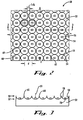
- Figure 2 is a top view of a portion of a dense LED array 50 as shown and described in the documents previously incorporated by reference. Although this array 50 omits certain aspects of the invention, it is described with reference to Figures 2 and 3 because it serves to illustrate aspects of, or relevant to, the invention.
- Array 50 is provided in a substrate 52 having a plurality of micro-reflector elements 54 formed therein.
- a LED 56 is provided within each micro-reflector element 54. Although only one LED is shown associated with a micro-reflector element 54, it is understood, as previously described, that each micro-reflector element 54 may be associated with more than one LED without departing from the principles of the invention.
- each of the micro-reflector elements 54 typically is an opening in the substrate 52, the opening being void or substantially void and having a selected volume and volumetric form, so as to accommodate the associated one or more LEDs.
- the elements 54 are shown implemented as openings in a substrate, it is understood that the elements 54 may be otherwise implemented without departing from the principles of the invention, including, e.g., being formed in a layer or other material disposed on top of the substrate or being formed in a combination of such layer or other material together with a substrate having openings.
- the substrate, layer and other materials may be any of a variety of materials, without departing from the principles of the invention.
- micro-reflector elements 54 may be implemented using various technologies. As examples, the micro-reflector elements may be formed using lithographical technology, machining, stamping, casting, forging, or other processes, or combinations of one or more of these. To illustrate, micro-reflector elements 54 may be formed by etching, so as to provide truncated, inverted, square pyramidal forms. To further illustrate, micro-reflector elements 54 may be formed by machining openings (e.g., via lasers and/or plasma). To illustrate still further, micro-reflector elements 54 may be formed by stamping parabolic forms in copper or other suitable material. To yet further illustrate, micro-reflector elements 54 may also be formed by a combination of etching, together with machining or other technology. In this further illustration, a substrate is etched to form openings. Each opening is then machined to provide desired shape or shapes.
- FIG 3 shows a side view of the LED array of Figure 2 , taken along line 3-3.
- Each micro-reflector element 54 includes one or more reflective surfaces 58. These reflective surface(s) 58 preferably are implemented so as to reflect one or more selected spectra of the radiant output(s) of the respective LEDs 56 of the array 50.
- the reflective surface(s) 58 may be implemented using various processes, including, as non-exhaustive examples, via selected metal or other coatings.
- each such micro-reflector element 54 also has a basic volumetric form.
- the basic volumetric form is the shape that provides the basis for the collection and collimation of the radiant output of the LEDs 56.
- the basic volumetric form correlates to a surface of revolution and, in particular, is illustrated as a hemispherical form.
- each such micro-reflector element 54 has an upper portion 55, a lower portion 57 and a longitudinal axis 59 there between.
- Each element 54 has a packing edge 60 disposed at the top of the upper portion 55.
- the packing edge 60 has a selected perimeter shape, the perimeter shape enclosing an area. The edge's perimeter shape is understood to contribute to the packing capabilities of the micro-reflector elements 54 in forming the array 50.
- the edge's perimeter shape is a circle.
- the perimeter shape is such because it is responsive to the volumetric form which is maintained in this micro-reflector element. Indeed, the perimeter shape will be a circle whenever the element maintains the volumetric form to the upper portion, because a circle is the outline of any cross-section of any volumetric form correlative to a surface of revolution.
- the array 50 provides for packing of LEDs 56 densely, but with some characteristics that provide avenues for enhancement.
- packing based on circular perimeter shapes leads to gaps 62 between the micro-reflector elements 54, in which gaps no LED is present to provide radiant output and no micro-reflector element collects or collimates.
- the packing is dense, but less dense than is possible, e.g., with micro-reflective elements having packing edges of non-circular perimeter shapes.
- example embodiments of a LED array in accordance with the invention tend to have at least one type of micro-reflector element characterized by a packing edge having a perimeter shape other than that responsive to the volumetric form, particularly if the volumetric form correlates to a surface of revolution. More generally, the packing edges of the micro-reflector array have one or more perimeter shapes selected so as to enhance mating among packing edges across the micro-reflector elements so as to enhance the packing density of the LED array in balance with collection and collimation of the emitting semiconductor devices' radiant output.
- FIG. 4 a top view is shown of a portion of a dense LED array 70, in accordance with the invention.
- Array 70 is provided in a substrate 72 having a plurality of micro-reflector elements 74 formed therein, such formation and implementation thereof being as previously described.
- a LED 76 is provided within each micro-reflector element 74. Again, although only one LED is shown associated with a micro-reflector element 74, it is understood, as previously described, that each micro-reflector element 74 may be associated with more than one LED 76, without departing from the principles of the invention.
- Each micro-reflector element 74 includes one or more reflective surfaces 78. These reflective surface(s) 78 preferably are implemented so as to reflect one or more selected spectra of the radiant output(s) of the respective LEDs 76.
- the reflective surface(s) 78 may be implemented using various processes, including, as non-exhaustive examples, via selected metal or other coatings.
- each such micro-reflector element 74 has a basic volumetric form.
- the basic volumetric form provides the basis for the collection and collimation of the radiant output of the LEDs 76.
- the basic volumetric form correlates to a volume resulting from a surface of revolution and, as in Figures 2 and 3 , is hemispherical.
- the hemispherical form of the element 74 is illustrated via the element's lower portion 80, together with phantom lines 82.
- the phantom lines 82 indicate that, as is described below and unlike as in Figures 2 and 3 , the micro-reflector element 74 does not maintain the basic volumetric form.
- a selected upper portion 84 of the element 74 follows a volumetric form or forms transitioning (here immediately, but in other embodiments, step-wise or smoothly) from the basic volumetric form so as to provide for the perimeter shape of the element's packing edge 86.
- Each micro-reflector element 74 has a packing edge 86.
- the packing edge 86 has a selected perimeter shape. As previously described, the perimeter shape is understood to contribute to the packing capabilities of the micro-reflector elements 74 in forming the array 70. As shown, the edge's perimeter shape is a square (i.e., father than the circle of Figures 2 and 3 ).
- micro-reflector array 70 of Figures 4 and 5 tend to mate along their adjacent edges (e.g., like tiles), thereby substantially eliminating the gaps 62 that are shown in Figures 2 and 3 .
- the micro-reflector elements 74 pack more closely center-to-center, so that the array 70 is more dense than the array 50 of Figures 2 and 3 .
- the " ⁇ " may vary depending on the selected area enclosed by the packing edge relative to the projected area of the opening at the upper portion of the micro-reflector were the micro-reflector to maintain the basic volumetric form.
- This is illustrated in Figure 6 in that the " ⁇ " between the projected area of the parabolic form at the upper portion 106, as delineate by phantom lines 115, will vary depending on the type and size of the perimeter shape 112 of the packing edge 110.
- " ⁇ " and thus packing density will generally be inversely proportional to changes in the size of hexagonal perimeter shape.
- While selecting a packing edge may result in denser packing, it is understood generally to result in an optical cost. As an example, that selection may reduce collimation of the radiant output of the LEDs 76 and, as such, potential reduction of radiant power density at or about the work piece 26.
- This is illustrated in Figure 9 , wherein a micro-reflector element 150 is shown, together with changes in volumetric form associated with various packing edge perimeter shapes 152a, 152b, 152c.
- the element 150 has reflective surfaces 154, which surfaces are implemented so as to collect and collimate the radiant output of a particular light emitting semiconductor 156.
- shapes 152a, 152b and 152c indicate that, as the perimeter shape's size decreases (152c>152b>152a) relative to the volumetric form, less and less of the surfaces 154 remain to collect and collimate.
- additional coupling optics 30, such as a microlens array disposed between the array 70 and the work piece 26, may be employed.
- such selection of the type and size of the perimeter shape(s) of a micro-reflector array - as well as, and in conjunction with, selection of other coupling optics, the volumetric form(s), the number, size, types and performance (e.g., near field radiation pattern) of LEDs deployed in each micro-reflector element, and the transition from the basic volumetric form to the perimeter shape - is directed toward optimizing high-density packing of the emitting semiconductor devices in the array in balance with collection and collimation of the devices' radiant output.
- FIG. 6 an example embodiment is shown of one LED 100 in a micro-reflector element 102, in accordance with the invention.
- the LED 100 is understood to be part of an LED array, the LED array being coupled with an micro-reflector array, which micro-reflector array includes a plurality of micro-reflector elements substantially the same as micro-reflector element 102.
- the micro-reflector element 102 has a lower portion 104 and an upper portion 106, and a longitudinal axis 108 oriented and extending therebetween.
- Such micro-reflector element 102 is a parabolic reflector; that is, the element 102 has a basic volumetric form correlating to a surface of revolution that forms a parabolic volume.
- the micro-reflector element's lower portion 104 generally has disposed thereat the LED 100. However, as previously, stated, a plurality of LEDs may be associated with the element 102 and, in that case, generally will be disposed at or about the lower portion 104.
- the micro-reflector element's upper portion 106 is characterized by a packing edge 110.
- the packing edge 110 has a selected perimeter shape 112, here a hexagon.
- this element's packing edge 110 has a perimeter shape 112 selected so as to enhance mating with the packing edges of the other micro-reflector elements (not shown) that are adjacent to this element in the array and decrease the separation, center-to-center, of the LEDs in the array.
- the perimeter shape preferably is also selected in contemplation of the effect such shape has on the collection and collimation of the radiant output of the LED (particularly, as such shape alters the micro-reflector's volumetric form.
- packing density of the LED array is enhanced in balance with the collection and collimation of the radiant output so as to optimize performance of the array, particularly in the context of the photoreactive application for which it is being employed.
- the micro-reflector array provides a common packing edge 110 for all its micro-reflector elements 102 (e.g., hexagons of the same size), it is understood that the array may be otherwise configured. That is, the micro-reflector array may be implemented to employ one micro-reflector element 102 having a packing edge 110 of one perimeter shape 112 and at least one other micro-reflector element having a packing edge 110 of a second perimeter shape 112.
- various combinations of perimeter shapes may be used without deviating from the principles of the invention, including: (a) one perimeter shape being a circle, with the other being a polygon; (b) both perimeter shapes being circles, but with different radii; and (c) both perimeter shapes being polygons, but the polygons being of different types and/or sizes (e.g., squares and octagons).
- the micro-reflector array includes more than one type of micro-reflector element
- the pluralities of each such type of elements typically are arranged in a selected pattern thereamong.
- Such patterns may employ off-sets among elements in order to enhance packing density Examples of these perimeter shapes and patterns, including use of off-sets, are shown in Figure 7 .
- volumetric forms include: (i) both elements correlating to the same type of surface of revolution (e.g., both parabolic), but having different size; (ii) each element correlating to a respective, but different type of surface of revolution (e.g., one parabolic and the other non- parabolic); (iii) one element correlating to a surface of revolution and the other being a selected polyhedron; and (iv) each element being associated with a respective, but different type and/or size of polyhedron. Any such form may be truncated at either/both the bottom or/and the top.
- the micro-reflector element 102 is fabricated so as to selectively transition in form along the longitudinal axis 108, at some point or range, between the elements' lower and upper portions 104, 106.
- the cross-section of the element 102 changes from the circles 116 given by the basic volumetric form (here, the parabolic form) to the polygons 118 given by the packing edge 110 (here, hexagons).
- the transition is indicated by the circle 116, in phantom lines, disposed in the lower portion 104 and by a portion of a hexagon 118, in phantom lines, disposed at a transition portion 120 of the element 102.
- the transition portion 120 is understood to include the range along the longitudinal axis 108, starting at initiation of the transition from the cross-section of the basic volumetric form and ending where the cross-section of the element 102 becomes the perimeter shape 112.
- the transition portion 120 is effectively a point along the longitudinal axis 108. That is, the transition is immediate, in that the perimeter shape 112 is established and unchanged from the upper portion 106 toward the lower portion 104, until its intersection with the basic volumetric form.
- transition may be accomplished by providing the exact, unchanged perimeter shape 112 of the packing edge 110 from the upper portion 106, toward the lower portion 104, until the perimeter shape 112 intersects the basic volumetric form. Doing so, effects an immediate transition at that intersection.
- the transition may also be accomplished by providing one or more intermediate cross-sectional shapes (e.g., in the transition portion, having neither the circle(s) of the basic volumetric form or the exact perimeter shape of the packing edge). This alternative effects a smooth or stepped transition along the longitudinal axis.
- FIG. 8 Examples of smooth and stepped transitions are shown in Figure 8 .
- the basic volumetric form is hemispheric and the packing edge's perimeter shape is square.
- an immediate transition is depicted by reference lines 112'. These lines 112' represent that the perimeter shape 112 is established and unchanged from the upper portion 106 toward the lower portion 104, until the transition portion 120 is established by intersection of the perimeter shape with the basic volumetric form.
- the perimeter shape is projected toward the lower portion, whereupon one or more cross-sections are used in transition between the perimeter shape (e.g., polygon) and the basic volumetric form's circles.
- phantom lines 114 show a stepped transition, as the perimeter shape is replaced by a cross-sectional shape providing two successively less-steep pitches before intersection with the basic volumetric shape.
- phantom lines 116 show a smooth transition, as the perimeter shape is replaced by a cross-sectional shape providing a continuously-curved line before intersection with the basic volumetric shape.
- the array preferably comprises part of light emitting subsystem 12 of photoreactive system 10, as previously described and shown in Figure 1 .
- the photoreactive system 10 includes cooling subsystem 18, implemented to manage the thermal behavior of the light emitting subsystem 12.
- the cooling subsystem 18 provides direct cooling of the semiconductor devices, in accordance with the disclosures shown and described in U.S. Patent Application US2005218468
- micro-reflector elements 200 include slots 202 disposed in the elements' respective lower portions. Coolant 204 is provided so as to enter through respective slots 202. Preferably, slots 202 are positioned below the focal point, which typically is the location of the semiconductor device 19. Coolant 204 flows through the slots (either by pressurization, convection, or otherwise, or both) and exits from the top of the elements 200. Coupling optics 30 preferably are employed, in part, to contain the coolant 204.
- semiconductor devices 19 are disposed in an array of micro-reflector elements 220.
- Coupling optics 30 is implemented having deflectors 222.
- these deflectors 222 like the coupling optics 30, have a selected index of refraction so as to minimize reflection of the radiant output (i.e., maximizing transmission to the work piece 26).
- one or more deflectors 222 are implemented having a selected shape, length and volume, and are dispose toward each device 19 and element 220.
- at least one such deflector 222 is centered, or substantially centered, on the respective element 220 (e.g., is aligned with the longitudinal axis of the element, as such axis is previously described for example embodiments).
- the deflector 222 so implemented arid disposed, divert a selected portion of the coolant 204 so as to flow into the respective element 220. Such diversion will tend to cause turbulence in the coolant (e.g., swirling around), which together with direct contact, cools the device 19. Although turbulence is indicated here, use of turbulence generally contemplates a balancing of its benefits (e.g., enhanced cooling performance) against its detriments.
Abstract
Description
- This application claims priority from
U.S. Provisional Application Serial Number 60/561,771, filed April 12, 2004 - This invention relates to high-density light emitting semiconductor device arrays and, more particularly, to a light emitting diode (LED) array having optical elements directed toward optimizing high-density packing of the LEDs in balance with collection and collimation of the LEDs' radiant output.
- From documents
EP 01 272 39 (A1 ),US 6,367,950 (B1 ),EP 0 326 668 (A2 ),US 6,527,411 (B1 );DE 2 941 634 (A1 ); andWO 03/096387 (A2 - Light-emitting semiconductor devices may be arranged in various configurations, such as arrays, for lighting applications. Examples of these applications include: lithographic processes used, e.g., in fabricating semiconductor devices, and curing processes used, e.g., for ink printing and fabrication of DVDs. These applications generally have associated parameters, including, e.g., a photoreaction may contemplate provision of one or more radiant power densities at the work surface, at one or more wavelengths, applied over one or more periods of time and within thermal limitations.
- In these applications, the light emitting semiconductor devices generally are employed to deliver against the parameter. At the same time, the light emitting semiconductor devices typically have certain operating characteristics and specifications. The characteristics include: total power emitted; power stability; radiance; radiant intensity; the wavelength(s) of the radiant output; the coherence of the radiant output; the collimation of the radiant output; as well as other operative functionalitles provided by the semiconductor device as a light system (e.g., ability to provide pulsed operation and/or effective thermal management). In turn, the light emitting semiconductor device's specifications generally are associated with its fabrication and, among other things, are directed to preclude destruction and/or forestall degradation of the devices. These specifications generally include operating temperatures and applied, electrical power.
- Where the application requires delivery of a relatively high radiant power density at or across the work surface, a LED array may have some difficulty in that delivery. That follows because a typical LED in an array has a widely distributed radiant output. Indeed, a typical LED mounted alone on a planar substrate will exhibit a radiant output distributed characteristically across the hemisphere centered at the LED. Given such distribution, only some portion, often relatively small, of that radiant output is directed toward the work surface, thus diminishing the radiant power density at or across the surface. Moreover, such distribution implicates that, as the work surface becomes more physically separated from the LED, the radiant power density at or across the work surface will decrease rapidly, i.e., the decrease generally is anticipated to be proportional to the square of the separation.
- Several approaches may be used to achieve radiant power density from a LED array so as to properly perform a particular process. In one example approach, a basic LED array may simply be disposed physically proximate the work surface. However, even if close proximity delivers appropriate power density, this approach generally is undesirable because, e.g., close proximity tends to necessitate undesirable changes to tooling and/or shielding. In another example approach, an array may locate conventional refractive lenses above the LEDs. This approach contemplates that each LED is associated with a conventional lens so that the lens collects and collimates the LED's radiant output. While this approach will tend to increase radiant power density, collecting and collimated a substantial preponderance of any LED's distributed radiant output contemplates a lens having a relatively large diameter, as well as other challenges. While this provides some performance increase, achieving the necessary diameter may be difficult, if not impossible. Moreover, using a lens of such diameter may be at odds with use of a densely-packed LED array and, as such, would be undesirable.
- Another example approach to enhancing radiant power density contemplates using conventional reflective optics. In this approach, a LED is mounted in a reflector (e.g., having a parabolic form). Unlike refractive optics, reflective optics generally collect and collimate a substantial portion of the LED's radiant output. Even so, conventional reflective optics generally are not used in a tightly packed or dense array because of their size. For example, a typical application of conventional reflective optics is illustrated by LED flashlights in which one or more LEDs are mounted in a large reflective optic, so that the optic collects light from such LEDs.
- Accordingly, there is a need for high-density light emitting semiconductor device array and, more particularly, for LED arrays having optical elements directed toward optimizing high-density packing of the LEDs in balance with collection and collimation of the LEDs' radiant output.
- An array of light emitting semiconductor devices in accordance with the invention is defined in claim 1 and includes optical elements selected toward optimizing high-density packing of the devices in the array in balance with collection and collimation of the devices' radiant output.
- In an example embodiment in accordance with the invention, an array of LEDs is coupled with a micro-reflector array, which micro-reflector array includes a plurality of micro-reflector elements. Each such micro-reflector element is a parabolic reflector, or otherwise has a basic volumetric form associated with a selected surface of revolution.
- Each such micro-reflector element has a lower portion and an upper portion. The upper portion is characterized by a packing edge having a selected perimeter shape. The perimeter shape, if responsive to the volumetric form, will be a circle, because this shape is the outline of any cross-section taken at the upper portion of an element having a volumetric form associated with a surface of revolution. Because circles do not pack as densely as may be desired and because, when packed, circles leave gaps there between, in this example embodiment, each individual element's packing edge preferably has a perimeter shape other than that responsive to the volumetric form. That is, the packing edge preferably has a perimeter shape selected so as to enhance mating with the packing edges of the micro-reflector elements adjacent such individual element in the array and, thereby, among other things, increase the packing density of the LED array. To illustrate, the packing edge typically is a selected polygon, such as a square or a hexagon.
- In other example embodiments, the micro-reflector array comprises more than one type of micro-reflector element, the pluralities of each such type of elements typically being arranged in a selected pattern thereamong. An example includes employing one micro-reflector element having a packing edge of one perimeter shape and another micro-reflector element having a packing edge of a second perimeter shape. In this example, various combinations of perimeter shapes may be used without deviating from the principles of the invention, including: (a) one perimeter shape being a circle, with the other being a polygon; (b) both perimeter shapes being circles, but with different radii and (c) both perimeter shapes being polygons, but the polygons being different in type and/or size (e.g., squares and octagons). In this example, as well, off-setting the micro-reflector elements in the array may be employed to enhance packing density. Moreover, in this example, the two elements' volumetric forms typically will be distinct, including: (i) both associated with the same type of surface of revolution (e.g., both parabolic), but having different size; (ii) each being associated with a respective, but different type of surface of revolution (e.g., one parabolic and the other non- parabolic); (iii) one associated with a surface of revolution and the other being a selected polyhedron; and (iv) each being associated with a respective, but different type or size of polyhedron.
- These and other embodiments are described in more detail in the following detailed descriptions and the figures.
- The foregoing is not intended to be an exhaustive list of embodiments and features of the present invention. Persons skilled in the art are capable of appreciating other embodiments and features from the following detailed description in conjunction with the drawings.
-
-
Figure 1 is a block diagram of a photoreactive system in accordance with the invention. -
Figure 2 is a top view of a portion of a dense LED array. -
Figure 3 shows a side view of the LED array ofFigure 2 , taken along line 3-3. -
Figure 4 is a top view of a portion of a dense LED array, in accordance with the invention. -
Figure 5 shows a side view of the LED array ofFigure 2 , taken along line 5-5. -
Figure 6 shows an example embodiment in accordance with the invention. -
Figure 7 shows examples of perimeter shapes and patterns, in accordance with the invention. -
Figure 8 shows examples of smooth and stepped transitions in micro-reflector elements, in accordance with the invention. -
Figure 9 shows a micro-reflector element, depicting change in volumetric form associated with various perimeter shapes, in accordance with the invention. -
Figure 10 shows a first approach for direct cooling an array, in accordance with the invention. -
Figure 11 shows a second approach for direct cooling an array, in accordance with the invention. -
Figure 1 is a block diagram of aphotoreactive system 10 in accordance with the invention. In this example embodiment, thephotoreactive system 10 comprises alight emitting subsystem 12, acontroller 14, apower source 16 and acooling subsystem 18. - The
light emitting subsystem 12 preferably comprises a plurality ofsemiconductor devices 19. The semiconductor devices provide aradiant output 24. Theradiant output 24 Is directed to awork piece 26. Returnedradiation 28 may be directed back to thelight emitting system 12 from the work piece 26 (e.g., via reflection of the radiant output 24). - The
radiant output 24 preferably is directed to thework piece 26 viacoupling optics 30. Thecoupling optics 30 include a micro-reflector array. In employing such micro-reflector array, each semiconductor device providingradiant output 24 is associated with a respective micro-reflector element on a selected basis. As an example, each micro-reflector element of the array may have one associated LED. As another example, each micro-reflector may have more than one associated LED, e.g., three LEDs, one emitting in the green spectrum, one emitting in the red spectrum and one emitting in the blue spectrum. Use of micro-reflector arrays, including various numbers, arrangements and other relationships of LEDs to micro-reflector elements, so as to enhance radiant output, is shown and described inUS 2005218468 entitled "MICRO-REFLECTORS ON A SUBSTRATE FOR HIGH-DENSITY LED ARRAY", - The
coupling optics 30 may also include other layers, materials, structure or other elements, any or all of which elements may be variously implemented without departing from the principles of this invention. Such one or more layers, materials or other structure may be interposed between thesemiconductor devices 19 and thework piece 26. As an example, thecoupling optics 30 may include one or more lenses, or a micro-lens array, disposed between thedevices 19 and thework piece 26, so as to enhance collection, condensing, or collimation of one or more device's radiant output and/or to otherwise improve the quality or effective quantity of the radiant output 24 (as well as the radiant power density at or about the work piece 26). - Preferably, each of the layers, materials or other structure of the
coupling optics 30 interposed in the path of the radiant output 24 (and/or returned radiation 28) have a selected index of refraction. By properly selecting each index of refraction, reflection at interfaces between layers, materials and other structure may be selectively controlled. As an example, by controlling differences in such indexes at a selected interface disposed between thesemiconductor devices 19 and thework piece 26, reflection at that interface may be controlled. Such control could be to reduce the reflection, toward eliminating or, at least, minimizing it, so as to enhance the transmission of radiant output at that interface for ultimate delivery to thework piece 26. Such control could also be to direct or re-direct selected radiation for other predetermined objectives. Control of indexes of refraction so as to enhance radiant output is shown and described in U.S. Patent ApplicationUS2005253252 - Coupling
optics 30 may be employed for various purposes. Example purposes include, among others, to protect thesemiconductor devices 19, to retain cooling fluid associated with thecooling subsystem 18, to collect, condense and/or collimate theradiant output 24, to collect, direct or reject returnedradiation 28, or for other purposes, alone or in combination. Generally, however, as described further herein,coupling optics 30 In accordance with the invention are employed and: implemented so as to enhance packing density of the devices in the array in balance with and while enhancing the effective quality or quantity of the devices' radiant output 24 (e.g., through collection and collimation), particularly as that output Is directed to thework piece 26. - Selected of the plurality of
semiconductor devices 19 may be coupled to thecontroller 14 viacoupling electronics 22, so as to provide data to thecontroller 14. As described further below, the controller preferably is also implemented to control such data-providing semiconductor devices, e.g., again viacoupling electronics 22. Thecontroller 14 preferably is also connected to, and implemented to control, each of thepower source 16 and thecooling subsystem 18. Moreover, thecontroller 14 preferably receives data from respectivesuch source 16 andsubsystem 18. - In addition to the
power source 16,cooling subsystem 18 and light emittingsubsystem 12, thecontroller 14 may also be connected to, and implemented to control,elements Element 32, as shown, is internal of thephotoreactive system 10.Element 34, as shown, is external of thephotoreactive system 10, but is understood to be associated with the work piece 26 (e.g., handling, cooling or other external equipment) or to be active in, or otherwise related to performance of, the photoreaction thesystem 10 supports. - The data received by the
controller 14 from one or more of thepower source 16, thecooling subsystem 18, thelight emitting subsystem 12, and/orelements semiconductor devices 19, respectively. As another example, the data may be representative of one or more characteristics associated with therespective component - The
controller 14, in receipt of any such data, preferably is implemented to respond to that data. Preferably, responsive to such data from any such component, thecontroller 14 is implemented to control one or more of thepower source 16,cooling subsystem 18, light emitting subsystem12 (including one or more such coupled semiconductor devices), and/or theelements controller 14 may be implemented to either (a) increase the power source's supply of power to one or more of the semiconductor devices, (b) increase cooling of the light emitting subsystem via the cooling subsystem 18 (i.e., certain light emitting devices, if cooled, provide greater radiant output), (c) increase the time during which the power is supplied to such devices, or (d) a combination of the above. - The
cooling subsystem 18 is implemented to manage the thermal behavior of thelight remitting subsystem 12. That is, generally, thecooling subsystem 18 provides for cooling ofsuch subsystem 12 and, more specifically, thesemiconductor devices 19. Thecooling subsystem 18 may also be implemented to cool thework piece 26 and/or the space between thepiece 26 and the photoreactive system 10 (e.g., particularly, the light emitting subsystem 12). Cooling systems providing thermal management in photoreactive systems generally, and providing for direct cooling of light emitting semiconductor devices in particular, are shown and described in U.S. Patent ApplicationUS2005218468 . - The
photoreactive systel 10 may be used for various applications. - Examples include, without limitation, curing applications ranging from ink printing to the fabrication of DVDs and lithography. Generally, the applications in which the
photoreactive system 10 is employed have associated parameters. That is, an application may contemplate parameters such as: provision of one or more levels of radiant power density, at one or more wavelengths, applied over one or more periods of time and within thermal limitations, In these applications, thesemiconductor devices 19 generally are employed to deliver against the parameters. However, thesemiconductor devices 19 topically have certain operating specifications, which specifications generally are associated with the semiconductor devices' fabrication and, among other things, should be followed In order to preclude destruction and/or forestall degradation of the devices. As well, other components of thesystem 10 also typically have associated operating specifications. These specifications generally include ranges (e.g., maximum and minimum) for operating temperatures and applied, electrical power. Accordingly, thephotoreactive system 10 preferably supports monitoring of the application's parameters. In addition, thephotoreactive system 10 preferably provides for monitoring of thesemiconductor devices 19, including as to respective characteristics and specifications. Moreover, thephotoreactive system 10 preferably also provides for monitoring of selected other components of thesystem 10, including as to respective characteristics and specifications. Providing such monitoring enables verification of the system's proper operation and, conversely, determination as to whether thesystem 10 is operating in any way other than property. Monitoring also supports control of the system's operation, such as to enable and/or enhance the system's proper operation and/or performance of the application (e.g., to balance between the array's radiant outputs and its operating temperature, so as to preclude heating the array beyond its specifications while also directing radiant energy to thework piece 26 sufficient to properly complete the photoreaction(s) of the application). Such monitoring and control in a photoreactive system is shown and described in U.S. Patent ApplicationUS2005230600 . entitled "LED ARRAY HALVING ARRAY-BASED LED DETECTORS", - Generally, it is recognized that some applications may require relatively high radiant power density at or about the work piece, so as to properly perform the application. Accordingly, it is desirable to implement a
light emitting subsystem 12 that can deliver such power density. To do so, thesubsystem 12 preferably is implemented using a dense array of light emittingsemiconductor devices 19. In particular, thesubsystem 12 preferably is implemented using a high-density, light emitting diode (LED) array. As previously described, the LED array preferably is associated withcoupling optics 30 in the form of a micro-reflector array. A high-density LED array is shown and described inU.S. Patent Application No. 10/984,589, filed November 8, 2004 US2005218468 . Although LED arrays may be used and are described in detail herein, it is understood that thesemiconductor devices 19, and array(s) 20 of same, may be implemented using other light emitting technologies without departing from the principles of the invention, which technologies include, without limitation, organic LEDs, laser diodes, and other semiconductor lasers. -
Figure 2 is a top view of a portion of adense LED array 50 as shown and described in the documents previously incorporated by reference. Although thisarray 50 omits certain aspects of the invention, it is described with reference toFigures 2 and 3 because it serves to illustrate aspects of, or relevant to, the invention. -
Array 50 is provided in asubstrate 52 having a plurality ofmicro-reflector elements 54 formed therein. ALED 56 is provided within eachmicro-reflector element 54. Although only one LED is shown associated with amicro-reflector element 54, it is understood, as previously described, that eachmicro-reflector element 54 may be associated with more than one LED without departing from the principles of the invention. - In this
array 50, each of themicro-reflector elements 54 typically is an opening in thesubstrate 52, the opening being void or substantially void and having a selected volume and volumetric form, so as to accommodate the associated one or more LEDs. Although theelements 54 are shown implemented as openings in a substrate, it is understood that theelements 54 may be otherwise implemented without departing from the principles of the invention, including, e.g., being formed in a layer or other material disposed on top of the substrate or being formed in a combination of such layer or other material together with a substrate having openings. The substrate, layer and other materials may be any of a variety of materials, without departing from the principles of the invention. - The
micro-reflector elements 54 may be implemented using various technologies. As examples, the micro-reflector elements may be formed using lithographical technology, machining, stamping, casting, forging, or other processes, or combinations of one or more of these. To illustrate,micro-reflector elements 54 may be formed by etching, so as to provide truncated, inverted, square pyramidal forms. To further illustrate,micro-reflector elements 54 may be formed by machining openings (e.g., via lasers and/or plasma). To illustrate still further,micro-reflector elements 54 may be formed by stamping parabolic forms in copper or other suitable material. To yet further illustrate,micro-reflector elements 54 may also be formed by a combination of etching, together with machining or other technology. In this further illustration, a substrate is etched to form openings. Each opening is then machined to provide desired shape or shapes. -
Figure 3 shows a side view of the LED array ofFigure 2 , taken along line 3-3. Eachmicro-reflector element 54 includes one or more reflective surfaces 58. These reflective surface(s) 58 preferably are implemented so as to reflect one or more selected spectra of the radiant output(s) of therespective LEDs 56 of thearray 50. The reflective surface(s) 58 may be implemented using various processes, including, as non-exhaustive examples, via selected metal or other coatings. - In this LED array, each such
micro-reflector element 54 also has a basic volumetric form. The basic volumetric form is the shape that provides the basis for the collection and collimation of the radiant output of theLEDs 56. Here, the basic volumetric form correlates to a surface of revolution and, in particular, is illustrated as a hemispherical form. - In turn, each such
micro-reflector element 54 has anupper portion 55, alower portion 57 and alongitudinal axis 59 there between. Eachelement 54 has a packingedge 60 disposed at the top of theupper portion 55. The packingedge 60 has a selected perimeter shape, the perimeter shape enclosing an area. The edge's perimeter shape is understood to contribute to the packing capabilities of themicro-reflector elements 54 in forming thearray 50. - As shown, the edge's perimeter shape is a circle. The perimeter shape is such because it is responsive to the volumetric form which is maintained in this micro-reflector element. Indeed, the perimeter shape will be a circle whenever the element maintains the volumetric form to the upper portion, because a circle is the outline of any cross-section of any volumetric form correlative to a surface of revolution.
- With circular perimeter shapes for the edges of all
micro-reflector elements 54, thearray 50 provides for packing ofLEDs 56 densely, but with some characteristics that provide avenues for enhancement. As an example, packing based on circular perimeter shapes leads togaps 62 between themicro-reflector elements 54, in which gaps no LED is present to provide radiant output and no micro-reflector element collects or collimates. In addition, the packing is dense, but less dense than is possible, e.g., with micro-reflective elements having packing edges of non-circular perimeter shapes. - Because circles do not pack as densely as may be desired and because, when packed, circles leave gaps there between, example embodiments of a LED array in accordance with the invention tend to have at least one type of micro-reflector element characterized by a packing edge having a perimeter shape other than that responsive to the volumetric form, particularly if the volumetric form correlates to a surface of revolution. More generally, the packing edges of the micro-reflector array have one or more perimeter shapes selected so as to enhance mating among packing edges across the micro-reflector elements so as to enhance the packing density of the LED array in balance with collection and collimation of the emitting semiconductor devices' radiant output.
- Turning to
Figure 4 , a top view is shown of a portion of adense LED array 70, in accordance with the invention.Array 70 is provided in asubstrate 72 having a plurality ofmicro-reflector elements 74 formed therein, such formation and implementation thereof being as previously described. ALED 76 is provided within eachmicro-reflector element 74. Again, although only one LED is shown associated with amicro-reflector element 74, it is understood, as previously described, that eachmicro-reflector element 74 may be associated with more than oneLED 76, without departing from the principles of the invention. - Turning to
Figure 5 , a side view is shown of theLED array 70 ofFigure 4 , taken along line 5-5. Eachmicro-reflector element 74 includes one or more reflective surfaces 78. These reflective surface(s) 78 preferably are implemented so as to reflect one or more selected spectra of the radiant output(s) of therespective LEDs 76. The reflective surface(s) 78 may be implemented using various processes, including, as non-exhaustive examples, via selected metal or other coatings. - In this
LED array 70, each suchmicro-reflector element 74 has a basic volumetric form. As previously described, the basic volumetric form provides the basis for the collection and collimation of the radiant output of theLEDs 76. Here, the basic volumetric form correlates to a volume resulting from a surface of revolution and, as inFigures 2 and 3 , is hemispherical. The hemispherical form of theelement 74 is illustrated via the element'slower portion 80, together withphantom lines 82. The phantom lines 82 indicate that, as is described below and unlike as inFigures 2 and 3 , themicro-reflector element 74 does not maintain the basic volumetric form. Rather a selectedupper portion 84 of theelement 74 follows a volumetric form or forms transitioning (here immediately, but in other embodiments, step-wise or smoothly) from the basic volumetric form so as to provide for the perimeter shape of the element'spacking edge 86. - Each
micro-reflector element 74 has a packingedge 86. The packingedge 86 has a selected perimeter shape. As previously described, the perimeter shape is understood to contribute to the packing capabilities of themicro-reflector elements 74 in forming thearray 70. As shown, the edge's perimeter shape is a square (i.e., father than the circle ofFigures 2 and 3 ). - Because of the edge's square perimeter shape, the elements of
micro-reflector array 70 ofFigures 4 and 5 tend to mate along their adjacent edges (e.g., like tiles), thereby substantially eliminating thegaps 62 that are shown inFigures 2 and 3 . Moreover, themicro-reflector elements 74 pack more closely center-to-center, so that thearray 70 is more dense than thearray 50 ofFigures 2 and 3 . As to the packing density, an illustrative comparison is shown in theFigures 2-5 : for thearray 50 ofFigures 2 and 3 , the distance betweenLEDs 56 center-to-center is "d", "d" being equivalent to the hemisphere's diameter, whereas, for thearray 70 ofFigures 4 and 5 , the distance between LEDs is "d-2Δ" where "d" is again the hemisphere's diameter and "Δ" is the lateral overlap of the element's hemisphere relative to each adjacent hemisphere. - In this illustration, it is understood that the "Δ" may vary depending on the selected area enclosed by the packing edge relative to the projected area of the opening at the upper portion of the micro-reflector were the micro-reflector to maintain the basic volumetric form. This is illustrated in
Figure 6 in that the "Δ" between the projected area of the parabolic form at theupper portion 106, as delineate byphantom lines 115, will vary depending on the type and size of theperimeter shape 112 of thepacking edge 110. As examples, "Δ", and thus packing density, will generally be inversely proportional to changes in the size of hexagonal perimeter shape. - To further illustrate increased packing density via selection of a square packing edge as shown in
Figures 4-5 , tworepresentative reflector elements 74 having square perimeter shapes are depicted inFigure 2 , together with an indication of the magnitude of 2Δ relative to the cross-sectional area of theupper portion 55 ofmicro-reflector element 54. - While selecting a packing edge may result in denser packing, it is understood generally to result in an optical cost. As an example, that selection may reduce collimation of the radiant output of the
LEDs 76 and, as such, potential reduction of radiant power density at or about thework piece 26. This is illustrated inFigure 9 , wherein amicro-reflector element 150 is shown, together with changes in volumetric form associated with various packing edge perimeter shapes 152a, 152b, 152c. Theelement 150 hasreflective surfaces 154, which surfaces are implemented so as to collect and collimate the radiant output of a particularlight emitting semiconductor 156. However, regardless of the type of perimeter shape,shapes surfaces 154 remain to collect and collimate. To address this optical cost, as previously described,additional coupling optics 30, such as a microlens array disposed between thearray 70 and thework piece 26, may be employed. More generally, though, as a central aspect of the invention, such selection of the type and size of the perimeter shape(s) of a micro-reflector array - as well as, and in conjunction with, selection of other coupling optics, the volumetric form(s), the number, size, types and performance (e.g., near field radiation pattern) of LEDs deployed in each micro-reflector element, and the transition from the basic volumetric form to the perimeter shape - is directed toward optimizing high-density packing of the emitting semiconductor devices in the array in balance with collection and collimation of the devices' radiant output. - Turning back to
Figure 6 , an example embodiment is shown of oneLED 100 in amicro-reflector element 102, in accordance with the invention. Here, theLED 100 is understood to be part of an LED array, the LED array being coupled with an micro-reflector array, which micro-reflector array includes a plurality of micro-reflector elements substantially the same asmicro-reflector element 102. - The
micro-reflector element 102 has alower portion 104 and anupper portion 106, and alongitudinal axis 108 oriented and extending therebetween. Suchmicro-reflector element 102 is a parabolic reflector; that is, theelement 102 has a basic volumetric form correlating to a surface of revolution that forms a parabolic volume. The micro-reflector element'slower portion 104 generally has disposed thereat theLED 100. However, as previously, stated, a plurality of LEDs may be associated with theelement 102 and, in that case, generally will be disposed at or about thelower portion 104. - The micro-reflector element's
upper portion 106 is characterized by apacking edge 110. Thepacking edge 110 has a selectedperimeter shape 112, here a hexagon. In this example embodiment, this element'spacking edge 110 has aperimeter shape 112 selected so as to enhance mating with the packing edges of the other micro-reflector elements (not shown) that are adjacent to this element in the array and decrease the separation, center-to-center, of the LEDs in the array. The perimeter shape preferably is also selected in contemplation of the effect such shape has on the collection and collimation of the radiant output of the LED (particularly, as such shape alters the micro-reflector's volumetric form. Thereby, packing density of the LED array is enhanced in balance with the collection and collimation of the radiant output so as to optimize performance of the array, particularly in the context of the photoreactive application for which it is being employed. - While this example embodiment suggests that the micro-reflector array provides a
common packing edge 110 for all its micro-reflector elements 102 (e.g., hexagons of the same size), it is understood that the array may be otherwise configured. That is, the micro-reflector array may be implemented to employ onemicro-reflector element 102 having a packingedge 110 of oneperimeter shape 112 and at least one other micro-reflector element having a packingedge 110 of asecond perimeter shape 112. In this example and other embodiments, various combinations of perimeter shapes may be used without deviating from the principles of the invention, including: (a) one perimeter shape being a circle, with the other being a polygon; (b) both perimeter shapes being circles, but with different radii; and (c) both perimeter shapes being polygons, but the polygons being of different types and/or sizes (e.g., squares and octagons). In such example embodiments where the micro-reflector array includes more than one type of micro-reflector element, the pluralities of each such type of elements typically are arranged in a selected pattern thereamong. Such patterns may employ off-sets among elements in order to enhance packing density Examples of these perimeter shapes and patterns, including use of off-sets, are shown inFigure 7 . - Moreover, in such example embodiments where two types of micro-reflector elements having different packing edges, such elements will also typically have distinct volumetric forms. Examples of various volumetric forms include: (i) both elements correlating to the same type of surface of revolution (e.g., both parabolic), but having different size; (ii) each element correlating to a respective, but different type of surface of revolution (e.g., one parabolic and the other non- parabolic); (iii) one element correlating to a surface of revolution and the other being a selected polyhedron; and (iv) each element being associated with a respective, but different type and/or size of polyhedron. Any such form may be truncated at either/both the bottom or/and the top.
- Turning back to
Figure 6 , in order to provide apacking edge 110 of any such selectedperimeter shape 112, themicro-reflector element 102 is fabricated so as to selectively transition in form along thelongitudinal axis 108, at some point or range, between the elements' lower andupper portions element 102 changes from thecircles 116 given by the basic volumetric form (here, the parabolic form) to thepolygons 118 given by the packing edge 110 (here, hexagons). - In
Figure 6 , the transition is indicated by thecircle 116, in phantom lines, disposed in thelower portion 104 and by a portion of ahexagon 118, in phantom lines, disposed at atransition portion 120 of theelement 102. Thetransition portion 120 is understood to include the range along thelongitudinal axis 108, starting at initiation of the transition from the cross-section of the basic volumetric form and ending where the cross-section of theelement 102 becomes theperimeter shape 112. Here, thetransition portion 120 is effectively a point along thelongitudinal axis 108. That is, the transition is immediate, in that theperimeter shape 112 is established and unchanged from theupper portion 106 toward thelower portion 104, until its intersection with the basic volumetric form. - As in
Figure 6 , transition may be accomplished by providing the exact,unchanged perimeter shape 112 of thepacking edge 110 from theupper portion 106, toward thelower portion 104, until theperimeter shape 112 intersects the basic volumetric form. Doing so, effects an immediate transition at that intersection. However, in the alternative, the transition may also be accomplished by providing one or more intermediate cross-sectional shapes (e.g., in the transition portion, having neither the circle(s) of the basic volumetric form or the exact perimeter shape of the packing edge). This alternative effects a smooth or stepped transition along the longitudinal axis. - Examples of smooth and stepped transitions are shown in
Figure 8 . InFigure 8 , for illustration, the basic volumetric form is hemispheric and the packing edge's perimeter shape is square. Again, an immediate transition is depicted byreference lines 112'. Theselines 112' represent that theperimeter shape 112 is established and unchanged from theupper portion 106 toward thelower portion 104, until thetransition portion 120 is established by intersection of the perimeter shape with the basic volumetric form. In the alternative, the perimeter shape is projected toward the lower portion, whereupon one or more cross-sections are used in transition between the perimeter shape (e.g., polygon) and the basic volumetric form's circles. More specifically,phantom lines 114 show a stepped transition, as the perimeter shape is replaced by a cross-sectional shape providing two successively less-steep pitches before intersection with the basic volumetric shape. In turn,phantom lines 116 show a smooth transition, as the perimeter shape is replaced by a cross-sectional shape providing a continuously-curved line before intersection with the basic volumetric shape. - Turning to
Figures 10 and 11 , two approaches are depicted relating to direct cooling of LEDs and/or other semiconductor devices used in a dense array, according to the invention. The array preferably comprises part of light emittingsubsystem 12 ofphotoreactive system 10, as previously described and shown inFigure 1 . Moreover, thephotoreactive system 10 includescooling subsystem 18, implemented to manage the thermal behavior of thelight emitting subsystem 12. Preferably, thecooling subsystem 18 provides direct cooling of the semiconductor devices, in accordance with the disclosures shown and described in U.S. Patent ApplicationUS2005218468 - In
Figure 10 ,micro-reflector elements 200 includeslots 202 disposed in the elements' respective lower portions.Coolant 204 is provided so as to enter throughrespective slots 202. Preferably,slots 202 are positioned below the focal point, which typically is the location of thesemiconductor device 19.Coolant 204 flows through the slots (either by pressurization, convection, or otherwise, or both) and exits from the top of theelements 200. Couplingoptics 30 preferably are employed, in part, to contain thecoolant 204. - In
Figure 11 ,semiconductor devices 19 are disposed in an array ofmicro-reflector elements 220. Couplingoptics 30 is implemented havingdeflectors 222. Typically, thesedeflectors 222, like thecoupling optics 30, have a selected index of refraction so as to minimize reflection of the radiant output (i.e., maximizing transmission to the work piece 26). Here, one ormore deflectors 222 are implemented having a selected shape, length and volume, and are dispose toward eachdevice 19 andelement 220. Preferably, at least onesuch deflector 222 is centered, or substantially centered, on the respective element 220 (e.g., is aligned with the longitudinal axis of the element, as such axis is previously described for example embodiments). Thedeflector 222, so implemented arid disposed, divert a selected portion of thecoolant 204 so as to flow into therespective element 220. Such diversion will tend to cause turbulence in the coolant (e.g., swirling around), which together with direct contact, cools thedevice 19. Although turbulence is indicated here, use of turbulence generally contemplates a balancing of its benefits (e.g., enhanced cooling performance) against its detriments. - Persons skilled in the art will recognize that many modifications and variations are possible in the details, materials, and arrangements of the parts and actions which have been described and illustrated in order to explain the nature of this invention and that such modifications and variations do not depart from the scope of the teachings and claims contained therein.
Claims (12)
- A dense array of light emitting semiconductor devices (19, 50, 70), the array providing radiant output (24) directed to a work piece (26), the array comprising:a plurality of first micro-reflector elements (54, 74, 102, 150, 200) wherein at least one such micro-reflector element has one or a plurality of associated light emitting semi-conductor devices, each such micro-reflector element having an upper portion (55, 106), a lower portion (57, 104) and a transition portion disposed between the upper and lower portions, each such element including a packing edge (60, 86, 110) disposed in the upper portion, the packing edge having a perimeter shape, each such element having a basic volumetric form, the cross-section of which volumetric form has a outline that differs from the perimeter shape of the packing edge and wherein, in the transition portion, the cross-section of the volumetric form transitions to provide for the perimeter shape, characterised in that said plurality of first the micro-reflector elements (54, 74, 102, 150) include slots (202) disposed in the lower portion, through which slots (202) coolant flows to directly cool the semiconductor devices.
- The dense array of claim 1, wherein at least one such micro-reflector element (54, 74.102.150, 200) has three light emitting diodes, one such diode emitting in the red spectrum, one emitting in the green spectrum and one emitting in the blue spectrum.
- The dense array of claim 1, wherein coupling optics interposed between the semiconductor devices (19, 56, 76 100, 156) and the work piece (26) comprise a lens structure.
- The dense array of claim 1, wherein the basic volumetric form correlates to a surface of revolution.
- The dense array of claim 4 wherein the volumetric form comprises at least one of a parabolic form a hemispherical form and a conic form
- The dense array of claim 4 wherein the volumetric form is truncated in one or both of the lower or upper portions of the element.
- The dense array of claims 1, wherein the basic volumetric form correlates to a polyhedron
- The dense array of claim 1, wherein the transition portion exhibits an immediate, smooth or stepped transition.
- The dense array of claims 8, wherein, at the interface between the transition portion and the upper portion (55, 106), the cross-section of the element has an outline congruent to the perimeter shape of the packing edge (60, 86, 110).
- The dense array of claim 1, further comprising a plurality of second micro-reflector elements, each such second micro-reflector element having an upper portion, a lower portion and a transition portion disposed between the upper and lower portions, each such second micro-reflector element including a packing edge disposed in the upper portion, the packing edge having a perimeter shape, each such second micro-reflector element having a basic volumetric form, the cross-section of which volumetric form has a outline that differs from the perimeter shape of the packing edge and wherein, in the transition portion, the cross-section of the volumetric form transitions to provide for the perimeter shape and, wherein the perimeter shape of the plurality of second micro-reflector elements differs from the perimeter shape of the plurality of first micro-reflector elements.
- The dense array of claim 1, wherein the perimeter shape is a polygon.
- A photoreactive system, the system (10) providing radiant output (24) directed to a work piece (26) in association with a photoreaction, the system (10) comprising:a light emitting subsystem, the light emitting subsystem including a dense array of light emitting semiconductor devices (19, 50, 70) according to one of claims 1 to 13. 3.
Priority Applications (1)
| Application Number | Priority Date | Filing Date | Title |
|---|---|---|---|
| PL05734339T PL1756876T3 (en) | 2004-04-12 | 2005-04-12 | High density led array |
Applications Claiming Priority (2)
| Application Number | Priority Date | Filing Date | Title |
|---|---|---|---|
| US56177104P | 2004-04-12 | 2004-04-12 | |
| PCT/US2005/012608 WO2005101535A2 (en) | 2004-04-12 | 2005-04-12 | High density led array |
Publications (3)
| Publication Number | Publication Date |
|---|---|
| EP1756876A2 EP1756876A2 (en) | 2007-02-28 |
| EP1756876A4 EP1756876A4 (en) | 2009-01-07 |
| EP1756876B1 true EP1756876B1 (en) | 2011-03-30 |
Family
ID=35150647
Family Applications (1)
| Application Number | Title | Priority Date | Filing Date |
|---|---|---|---|
| EP05734339A Active EP1756876B1 (en) | 2004-04-12 | 2005-04-12 | High density led array |
Country Status (9)
| Country | Link |
|---|---|
| US (2) | US7071493B2 (en) |
| EP (1) | EP1756876B1 (en) |
| AT (1) | ATE503963T1 (en) |
| DE (1) | DE602005027201D1 (en) |
| DK (1) | DK1756876T3 (en) |
| ES (1) | ES2363435T3 (en) |
| PL (1) | PL1756876T3 (en) |
| PT (1) | PT1756876E (en) |
| WO (1) | WO2005101535A2 (en) |
Families Citing this family (50)
| Publication number | Priority date | Publication date | Assignee | Title |
|---|---|---|---|---|
| TWI229946B (en) * | 2002-05-08 | 2005-03-21 | Phoseon Technology Inc | High efficiency solid-state light source and methods of use and manufacture |
| JP3773525B2 (en) * | 2003-08-07 | 2006-05-10 | 松下電器産業株式会社 | LED lighting source |
| US7524085B2 (en) * | 2003-10-31 | 2009-04-28 | Phoseon Technology, Inc. | Series wiring of highly reliable light sources |
| US7819550B2 (en) * | 2003-10-31 | 2010-10-26 | Phoseon Technology, Inc. | Collection optics for led array with offset hemispherical or faceted surfaces |
| WO2005090686A2 (en) * | 2004-03-15 | 2005-09-29 | Onscreen Technologies, Inc. | Rapid dispatch emergency signs |
| WO2005091392A1 (en) | 2004-03-18 | 2005-09-29 | Phoseon Technology, Inc. | Micro-reflectors on a substrate for high-density led array |
| US7235878B2 (en) | 2004-03-18 | 2007-06-26 | Phoseon Technology, Inc. | Direct cooling of LEDs |
| EP1743384B1 (en) * | 2004-03-30 | 2015-08-05 | Phoseon Technology, Inc. | Led array having array-based led detectors |
| WO2005101535A2 (en) * | 2004-04-12 | 2005-10-27 | Phoseon Technology, Inc. | High density led array |
| US8077305B2 (en) * | 2004-04-19 | 2011-12-13 | Owen Mark D | Imaging semiconductor structures using solid state illumination |
| US7138659B2 (en) * | 2004-05-18 | 2006-11-21 | Onscreen Technologies, Inc. | LED assembly with vented circuit board |
| JP4800324B2 (en) * | 2004-12-30 | 2011-10-26 | フォーセン テクノロジー インク | Exposure equipment |
| US7932535B2 (en) * | 2005-11-02 | 2011-04-26 | Nuventix, Inc. | Synthetic jet cooling system for LED module |
| US7642527B2 (en) * | 2005-12-30 | 2010-01-05 | Phoseon Technology, Inc. | Multi-attribute light effects for use in curing and other applications involving photoreactions and processing |
| US8044412B2 (en) | 2006-01-20 | 2011-10-25 | Taiwan Semiconductor Manufacturing Company, Ltd | Package for a light emitting element |
| US7521726B2 (en) | 2006-03-15 | 2009-04-21 | Illinois Tool Works Inc. | Collimated LED array with reflector |
| US7637628B2 (en) * | 2006-06-13 | 2009-12-29 | Light-Pod, Inc. | LED light pod with modular optics and heat dissipation structure |
| US7784972B2 (en) * | 2006-12-22 | 2010-08-31 | Nuventix, Inc. | Thermal management system for LED array |
| TWI336962B (en) * | 2007-02-08 | 2011-02-01 | Touch Micro System Tech | White light emitting diode package structure having silicon substrate and method of making the same |
| TW200834962A (en) * | 2007-02-08 | 2008-08-16 | Touch Micro System Tech | LED array package structure having Si-substrate and method of making the same |
| TW200837974A (en) * | 2007-03-01 | 2008-09-16 | Touch Micro System Tech | Light emitting diode package structure and manufacturing method thereof |
| US20090050921A1 (en) * | 2007-08-23 | 2009-02-26 | Philips Lumileds Lighting Company Llc | Light Emitting Diode Array |
| US20100067224A1 (en) * | 2007-08-24 | 2010-03-18 | Yu-Chao Wu | Light emitting system |
| KR100891810B1 (en) * | 2007-11-06 | 2009-04-07 | 삼성전기주식회사 | White light emitting device |
| US20090154137A1 (en) * | 2007-12-14 | 2009-06-18 | Philips Lumileds Lighting Company, Llc | Illumination Device Including Collimating Optics |
| JP5517418B2 (en) * | 2008-04-30 | 2014-06-11 | キヤノン株式会社 | Light emitting device |
| US8578854B2 (en) * | 2008-05-23 | 2013-11-12 | Esko-Graphics Imaging Gmbh | Curing of photo-curable printing plates using a light tunnel of mirrored walls and having a polygonal cross-section like a kaleidoscope |
| US20110116262A1 (en) * | 2009-11-13 | 2011-05-19 | Phoseon Technology, Inc. | Economical partially collimating reflective micro optical array |
| EP2532946A4 (en) * | 2010-02-05 | 2013-10-02 | With Ltd Liability Dis Plus Soc | Method for producing a light-radiating surface and a lighting device for implementing the method |
| US8581269B2 (en) | 2010-02-10 | 2013-11-12 | Lumen Dynamics Group Inc. | Modular high density LED array light sources |
| US8198109B2 (en) | 2010-08-27 | 2012-06-12 | Quarkstar Llc | Manufacturing methods for solid state light sheet or strip with LEDs connected in series for general illumination |
| US8415704B2 (en) | 2010-09-22 | 2013-04-09 | Ut-Battelle, Llc | Close-packed array of light emitting devices |
| US8192051B2 (en) | 2010-11-01 | 2012-06-05 | Quarkstar Llc | Bidirectional LED light sheet |
| DE102011086915A1 (en) | 2011-01-26 | 2012-07-26 | Carl Zeiss Smt Gmbh | Illumination system for microlithographic projection exposure system, has LED for generating illumination radiation in UV range at specific wavelength |
| US8314566B2 (en) | 2011-02-22 | 2012-11-20 | Quarkstar Llc | Solid state lamp using light emitting strips |
| US8410726B2 (en) | 2011-02-22 | 2013-04-02 | Quarkstar Llc | Solid state lamp using modular light emitting elements |
| US8485691B2 (en) | 2011-05-13 | 2013-07-16 | Lumenpulse Lighting, Inc. | High powered light emitting diode lighting unit |
| DE102011107893A1 (en) * | 2011-07-18 | 2013-01-24 | Heraeus Noblelight Gmbh | Optoelectronic module with improved optics |
| EP2872337B1 (en) | 2012-07-12 | 2022-03-30 | HP Scitex Ltd | Led illuminaton source |
| US20140357425A1 (en) * | 2013-05-31 | 2014-12-04 | Nike, Inc. | Golf ball with visible light-cured coating and method |
| KR102086359B1 (en) * | 2013-08-23 | 2020-03-10 | 삼성전자주식회사 | Light emitting module |
| US9752748B2 (en) | 2013-12-05 | 2017-09-05 | Martin Professional Aps | Projecting light fixture with a plurality of lenslets packed in an optimized dense circular pattern |
| US20160106872A1 (en) * | 2014-10-17 | 2016-04-21 | Seth Martinez | Handheld device for destroying microorganisms |
| KR101671808B1 (en) * | 2014-12-03 | 2016-11-03 | 주식회사 필옵틱스 | Uv cure apparatus using light emitting diode |
| US10209005B2 (en) | 2015-10-05 | 2019-02-19 | Sunlite Science & Technology, Inc. | UV LED systems and methods |
| US10712669B2 (en) | 2015-12-30 | 2020-07-14 | Asml Netherlands B.V. | Method and apparatus for direct write maskless lithography |
| CN108700820B (en) | 2015-12-30 | 2021-07-09 | Asml荷兰有限公司 | Method and apparatus for direct write maskless lithography |
| WO2017114653A1 (en) | 2015-12-30 | 2017-07-06 | Asml Netherlands B.V. | Method and apparatus for direct write maskless lithography |
| TWM535782U (en) * | 2016-09-22 | 2017-01-21 | Excellence Opto Inc | Structure of light-emitting-diode array light-cup with focus positioning function |
| US10687478B2 (en) | 2018-09-21 | 2020-06-23 | Austin Rouse | Optimized LED lighting array for horticultural applications |
Family Cites Families (87)
| Publication number | Priority date | Publication date | Assignee | Title |
|---|---|---|---|---|
| GB1218852A (en) * | 1968-04-02 | 1971-01-13 | English Electric Co Ltd | High voltage thyristor equipment |
| US4435732A (en) * | 1973-06-04 | 1984-03-06 | Hyatt Gilbert P | Electro-optical illumination control system |
| US4011575A (en) * | 1974-07-26 | 1977-03-08 | Litton Systems, Inc. | Light emitting diode array having a plurality of conductive paths for each light emitting diode |
| US4271408A (en) | 1978-10-17 | 1981-06-02 | Stanley Electric Co., Ltd. | Colored-light emitting display |
| FR2547087B1 (en) * | 1983-05-30 | 1985-07-12 | Radiotechnique Compelec | SEMICONDUCTOR CRYSTAL DISPLAY PANEL ELEMENT AND PANEL COMPRISING SAID ELEMENT |
| US4595289A (en) * | 1984-01-25 | 1986-06-17 | At&T Bell Laboratories | Inspection system utilizing dark-field illumination |
| JPH0825302B1 (en) * | 1984-09-27 | 1996-03-13 | Sanyo Denki Kk | |
| US4684801A (en) * | 1986-02-28 | 1987-08-04 | Carroll Touch Inc. | Signal preconditioning for touch entry device |
| KR880014692A (en) * | 1987-05-30 | 1988-12-24 | 강진구 | Semiconductor Light Emitting Device with Reflector |
| JPH01197141A (en) | 1988-02-02 | 1989-08-08 | Stanley Electric Co Ltd | Rear combination lamp for automobile |
| EP0454174B1 (en) * | 1990-04-27 | 1997-03-05 | Omron Corporation | Light emitting semiconductor device with Fresnel lens |
| US5150623A (en) * | 1990-07-17 | 1992-09-29 | The Boeing Company | Inspection device for flush head bolts and rivets |
| US5195102A (en) * | 1991-09-13 | 1993-03-16 | Litton Systems Inc. | Temperature controlled laser diode package |
| JP3025109B2 (en) * | 1992-03-11 | 2000-03-27 | シャープ株式会社 | Light source and light source device |
| US5397867A (en) * | 1992-09-04 | 1995-03-14 | Lucas Industries, Inc. | Light distribution for illuminated keyboard switches and displays |
| JPH06301304A (en) * | 1993-02-19 | 1994-10-28 | Minolta Camera Co Ltd | Fixing device |
| FR2707223B1 (en) * | 1993-07-07 | 1995-09-29 | Valeo Vision | Improved signaling light with light-emitting diodes. |
| US5424544A (en) * | 1994-04-29 | 1995-06-13 | Texas Instruments Incorporated | Inter-pixel thermal isolation for hybrid thermal detectors |
| US5632551A (en) * | 1994-07-18 | 1997-05-27 | Grote Industries, Inc. | LED vehicle lamp assembly |
| US5698866A (en) * | 1994-09-19 | 1997-12-16 | Pdt Systems, Inc. | Uniform illuminator for phototherapy |
| US5660461A (en) * | 1994-12-08 | 1997-08-26 | Quantum Devices, Inc. | Arrays of optoelectronic devices and method of making same |
| US5522225A (en) * | 1994-12-19 | 1996-06-04 | Xerox Corporation | Thermoelectric cooler and temperature sensor subassembly with improved temperature control |
| US5554849A (en) * | 1995-01-17 | 1996-09-10 | Flir Systems, Inc. | Micro-bolometric infrared staring array |
| US5623510A (en) * | 1995-05-08 | 1997-04-22 | The United States Of America As Represented By The United States Department Of Energy | Tunable, diode side-pumped Er: YAG laser |
| SG42307A1 (en) * | 1996-01-09 | 1997-08-15 | Peng Seng Toh | Measurement and inspection of leads on integrated circuit packages |
| US5806965A (en) * | 1996-01-30 | 1998-09-15 | R&M Deese, Inc. | LED beacon light |
| IL118872A (en) * | 1996-07-16 | 2000-06-01 | Orbot Instr Ltd | Optical inspection method and apparatus |
| US6058012A (en) * | 1996-08-26 | 2000-05-02 | Compaq Computer Corporation | Apparatus, method and system for thermal management of an electronic system having semiconductor devices |
| US5857767A (en) * | 1996-09-23 | 1999-01-12 | Relume Corporation | Thermal management system for L.E.D. arrays |
| US5715270A (en) * | 1996-09-27 | 1998-02-03 | Mcdonnell Douglas Corporation | High efficiency, high power direct diode laser systems and methods therefor |
| US5877899A (en) * | 1997-05-13 | 1999-03-02 | Northeast Robotics Llc | Imaging system and method for imaging indicia on wafer |
| US6163036A (en) * | 1997-09-15 | 2000-12-19 | Oki Data Corporation | Light emitting element module with a parallelogram-shaped chip and a staggered chip array |
| US6200134B1 (en) * | 1998-01-20 | 2001-03-13 | Kerr Corporation | Apparatus and method for curing materials with radiation |
| US6239702B1 (en) * | 1998-03-10 | 2001-05-29 | Raytheon Company | Electromagnetic energy detection |
| US6088185A (en) * | 1998-06-05 | 2000-07-11 | Seagate Technology, Inc. | Rotational vibration detection using a velocity sense coil |
| US6536923B1 (en) * | 1998-07-01 | 2003-03-25 | Sidler Gmbh & Co. | Optical attachment for a light-emitting diode and brake light for a motor vehicle |
| JP3195294B2 (en) * | 1998-08-27 | 2001-08-06 | スタンレー電気株式会社 | Vehicle lighting |
| US6291839B1 (en) * | 1998-09-11 | 2001-09-18 | Lulileds Lighting, U.S. Llc | Light emitting device having a finely-patterned reflective contact |
| US6534791B1 (en) * | 1998-11-27 | 2003-03-18 | Lumileds Lighting U.S., Llc | Epitaxial aluminium-gallium nitride semiconductor substrate |
| US20010042866A1 (en) * | 1999-02-05 | 2001-11-22 | Carrie Carter Coman | Inxalygazn optical emitters fabricated via substrate removal |
| US6320206B1 (en) * | 1999-02-05 | 2001-11-20 | Lumileds Lighting, U.S., Llc | Light emitting devices having wafer bonded aluminum gallium indium nitride structures and mirror stacks |
| DE19931689A1 (en) * | 1999-07-08 | 2001-01-11 | Patent Treuhand Ges Fuer Elektrische Gluehlampen Mbh | Planar LED assembly on thermally-conductive board, increases cooling, component packing density and life, whilst permitting active device integration to form display- or illumination panel in or on e.g. vehicle |
| TW457732B (en) * | 1999-08-27 | 2001-10-01 | Lumileds Lighting Bv | Luminaire, optical element and method of illuminating an object |
| JP4131891B2 (en) * | 1999-09-03 | 2008-08-13 | ローム株式会社 | Lens array and method for manufacturing lens array |
| US6788895B2 (en) * | 1999-12-10 | 2004-09-07 | Altera Corporation | Security mapping and auto reconfiguration |
| US6318886B1 (en) * | 2000-02-11 | 2001-11-20 | Whelen Engineering Company | High flux led assembly |
| US7320593B2 (en) * | 2000-03-08 | 2008-01-22 | Tir Systems Ltd. | Light emitting diode light source for curing dental composites |
| US6419384B1 (en) * | 2000-03-24 | 2002-07-16 | Buztronics Inc | Drinking vessel with indicator activated by inertial switch |
| KR100869866B1 (en) * | 2000-06-29 | 2008-11-24 | 코닌클리즈케 필립스 일렉트로닉스 엔.브이. | Optoelectric element |
| JP4142234B2 (en) * | 2000-07-04 | 2008-09-03 | 株式会社エンプラス | Surface light source device and liquid crystal display device |
| US6527411B1 (en) * | 2000-08-01 | 2003-03-04 | Visteon Corporation | Collimating lamp |
| US6578989B2 (en) * | 2000-09-29 | 2003-06-17 | Omron Corporation | Optical device for an optical element and apparatus employing the device |
| US7714301B2 (en) * | 2000-10-27 | 2010-05-11 | Molecular Devices, Inc. | Instrument excitation source and calibration method |
| US6525335B1 (en) * | 2000-11-06 | 2003-02-25 | Lumileds Lighting, U.S., Llc | Light emitting semiconductor devices including wafer bonded heterostructures |
| GB2369428B (en) * | 2000-11-22 | 2004-11-10 | Imperial College | Detection system |
| CA2332190A1 (en) * | 2001-01-25 | 2002-07-25 | Efos Inc. | Addressable semiconductor array light source for localized radiation delivery |
| US7075112B2 (en) * | 2001-01-31 | 2006-07-11 | Gentex Corporation | High power radiation emitter device and heat dissipating package for electronic components |
| US6547249B2 (en) * | 2001-03-29 | 2003-04-15 | Lumileds Lighting U.S., Llc | Monolithic series/parallel led arrays formed on highly resistive substrates |
| US6755647B2 (en) * | 2001-04-26 | 2004-06-29 | New Photonics, Llc | Photocuring device with axial array of light emitting diodes and method of curing |
| US6607286B2 (en) * | 2001-05-04 | 2003-08-19 | Lumileds Lighting, U.S., Llc | Lens and lens cap with sawtooth portion for light emitting diode |
| US6630689B2 (en) * | 2001-05-09 | 2003-10-07 | Lumileds Lighting, U.S. Llc | Semiconductor LED flip-chip with high reflectivity dielectric coating on the mesa |
| US6578986B2 (en) * | 2001-06-29 | 2003-06-17 | Permlight Products, Inc. | Modular mounting arrangement and method for light emitting diodes |
| US6551217B2 (en) * | 2001-07-10 | 2003-04-22 | Yuriy Kaganovsky | Combination exercise apparatus |
| US6785001B2 (en) * | 2001-08-21 | 2004-08-31 | Silicon Light Machines, Inc. | Method and apparatus for measuring wavelength jitter of light signal |
| JP4067802B2 (en) * | 2001-09-18 | 2008-03-26 | 松下電器産業株式会社 | Lighting device |
| US6498355B1 (en) * | 2001-10-09 | 2002-12-24 | Lumileds Lighting, U.S., Llc | High flux LED array |
| US6561640B1 (en) * | 2001-10-31 | 2003-05-13 | Xerox Corporation | Systems and methods of printing with ultraviolet photosensitive resin-containing materials using light emitting devices |
| US6480389B1 (en) * | 2002-01-04 | 2002-11-12 | Opto Tech Corporation | Heat dissipation structure for solid-state light emitting device package |
| US6796698B2 (en) * | 2002-04-01 | 2004-09-28 | Gelcore, Llc | Light emitting diode-based signal light |
| TWI229946B (en) * | 2002-05-08 | 2005-03-21 | Phoseon Technology Inc | High efficiency solid-state light source and methods of use and manufacture |
| DE10223201C1 (en) * | 2002-05-24 | 2003-05-28 | Fraunhofer Ges Forschung | Optical detection device for optical data has primary detection diode and secondary detection diodes coupled to respective read-out circuits with different read-out rates |
| US6573536B1 (en) * | 2002-05-29 | 2003-06-03 | Optolum, Inc. | Light emitting diode light source |
| US20040134603A1 (en) * | 2002-07-18 | 2004-07-15 | Hideo Kobayashi | Method and apparatus for curing adhesive between substrates, and disc substrate bonding apparatus |
| US6822991B2 (en) * | 2002-09-30 | 2004-11-23 | Lumileds Lighting U.S., Llc | Light emitting devices including tunnel junctions |
| US6880954B2 (en) * | 2002-11-08 | 2005-04-19 | Smd Software, Inc. | High intensity photocuring system |
| US6708501B1 (en) * | 2002-12-06 | 2004-03-23 | Nanocoolers, Inc. | Cooling of electronics by electrically conducting fluids |
| TW571449B (en) * | 2002-12-23 | 2004-01-11 | Epistar Corp | Light-emitting device having micro-reflective structure |
| US7211299B2 (en) * | 2003-01-09 | 2007-05-01 | Con-Trol-Cure, Inc. | UV curing method and apparatus |
| US7465909B2 (en) * | 2003-01-09 | 2008-12-16 | Con-Trol-Cure, Inc. | UV LED control loop and controller for causing emitting UV light at a much greater intensity for UV curing |
| US7175712B2 (en) * | 2003-01-09 | 2007-02-13 | Con-Trol-Cure, Inc. | Light emitting apparatus and method for curing inks, coatings and adhesives |
| US7102172B2 (en) * | 2003-10-09 | 2006-09-05 | Permlight Products, Inc. | LED luminaire |
| US7179670B2 (en) * | 2004-03-05 | 2007-02-20 | Gelcore, Llc | Flip-chip light emitting diode device without sub-mount |
| WO2005091392A1 (en) * | 2004-03-18 | 2005-09-29 | Phoseon Technology, Inc. | Micro-reflectors on a substrate for high-density led array |
| US7235878B2 (en) * | 2004-03-18 | 2007-06-26 | Phoseon Technology, Inc. | Direct cooling of LEDs |
| EP1743384B1 (en) * | 2004-03-30 | 2015-08-05 | Phoseon Technology, Inc. | Led array having array-based led detectors |
| WO2005101535A2 (en) * | 2004-04-12 | 2005-10-27 | Phoseon Technology, Inc. | High density led array |
| US8077305B2 (en) * | 2004-04-19 | 2011-12-13 | Owen Mark D | Imaging semiconductor structures using solid state illumination |
-
2005
- 2005-04-12 WO PCT/US2005/012608 patent/WO2005101535A2/en active Application Filing
- 2005-04-12 EP EP05734339A patent/EP1756876B1/en active Active
- 2005-04-12 DK DK05734339.4T patent/DK1756876T3/en active
- 2005-04-12 PT PT05734339T patent/PT1756876E/en unknown
- 2005-04-12 AT AT05734339T patent/ATE503963T1/en active
- 2005-04-12 PL PL05734339T patent/PL1756876T3/en unknown
- 2005-04-12 ES ES05734339T patent/ES2363435T3/en active Active
- 2005-04-12 US US11/104,954 patent/US7071493B2/en active Active
- 2005-04-12 DE DE602005027201T patent/DE602005027201D1/en active Active
-
2006
- 2006-05-12 US US11/434,544 patent/US20070051964A1/en not_active Abandoned
Also Published As
| Publication number | Publication date |
|---|---|
| US20050247947A1 (en) | 2005-11-10 |
| US7071493B2 (en) | 2006-07-04 |
| ATE503963T1 (en) | 2011-04-15 |
| DE602005027201D1 (en) | 2011-05-12 |
| WO2005101535A2 (en) | 2005-10-27 |
| EP1756876A2 (en) | 2007-02-28 |
| US20070051964A1 (en) | 2007-03-08 |
| PT1756876E (en) | 2011-06-02 |
| EP1756876A4 (en) | 2009-01-07 |
| DK1756876T3 (en) | 2011-07-18 |
| PL1756876T3 (en) | 2011-10-31 |
| ES2363435T3 (en) | 2011-08-04 |
| WO2005101535A3 (en) | 2007-04-05 |
Similar Documents
| Publication | Publication Date | Title |
|---|---|---|
| EP1756876B1 (en) | High density led array | |
| US8485692B2 (en) | LED-based light source with sharply defined field angle | |
| KR101241474B1 (en) | Illumination device with light emitting diodes and movable light adjustment member | |
| EP2789897B1 (en) | Light source and illuminating device | |
| KR200485222Y1 (en) | Linear fresnel optic for reducing angular spread of light from led array | |
| JP5395801B2 (en) | LIGHTING DEVICE WITH LIGHT EMITTING DIODE | |
| TWI518875B (en) | Coating method for an optoelectronic chip-on-board module | |
| US8487519B2 (en) | Light emitting device | |
| US20080025047A1 (en) | Light source comprising edge emitting elements | |
| US20120257386A1 (en) | Led based illumination module with a reflective mask | |
| US20110025190A1 (en) | Luminous device | |
| CA2749498A1 (en) | Led lens | |
| WO2002097325A1 (en) | Multiple source collimated beam luminaire | |
| TWI640412B (en) | Curing device and method with multi-wavelength led | |
| WO2013088296A1 (en) | Optical arrangement with diffractive optics | |
| KR200484992Y1 (en) | Edge weighted spacing of leds for improved uniformity range | |
| KR20160056089A (en) | Light emitting apparatus | |
| JP7073591B2 (en) | Improved thermal management in laser-based lighting with faceted ball lenses | |
| US11499695B2 (en) | Optical member and light emission device | |
| US20110149565A1 (en) | Lighting module with diffractive optical element | |
| JP2016111340A (en) | Lighting device with faceted reflector | |
| JP2021144858A (en) | Light source device, optical lens and method for manufacturing optical lens |
Legal Events
| Date | Code | Title | Description |
|---|---|---|---|
| PUAI | Public reference made under article 153(3) epc to a published international application that has entered the european phase |
Free format text: ORIGINAL CODE: 0009012 |
|
| 17P | Request for examination filed |
Effective date: 20061110 |
|
| AK | Designated contracting states |
Kind code of ref document: A2 Designated state(s): AT BE BG CH CY CZ DE DK EE ES FI FR GB GR HU IE IS IT LI LT LU MC NL PL PT RO SE SI SK TR |
|
| AX | Request for extension of the european patent |
Extension state: AL BA HR LV MK YU |
|
| PUAK | Availability of information related to the publication of the international search report |
Free format text: ORIGINAL CODE: 0009015 |
|
| DAX | Request for extension of the european patent (deleted) | ||
| A4 | Supplementary search report drawn up and despatched |
Effective date: 20081205 |
|
| RIC1 | Information provided on ipc code assigned before grant |
Ipc: H01L 33/00 20060101ALI20081202BHEP Ipc: F21K 7/00 20060101AFI20081202BHEP |
|
| 17Q | First examination report despatched |
Effective date: 20090211 |
|
| GRAP | Despatch of communication of intention to grant a patent |
Free format text: ORIGINAL CODE: EPIDOSNIGR1 |
|
| RIC1 | Information provided on ipc code assigned before grant |
Ipc: H01L 33/00 20100101ALI20100707BHEP Ipc: F21K 99/00 20100101AFI20100707BHEP |
|
| GRAS | Grant fee paid |
Free format text: ORIGINAL CODE: EPIDOSNIGR3 |
|
| GRAA | (expected) grant |
Free format text: ORIGINAL CODE: 0009210 |
|
| AK | Designated contracting states |
Kind code of ref document: B1 Designated state(s): AT BE BG CH CY CZ DE DK EE ES FI FR GB GR HU IE IS IT LI LT LU MC NL PL PT RO SE SI SK TR |
|
| REG | Reference to a national code |
Ref country code: GB Ref legal event code: FG4D |
|
| REG | Reference to a national code |
Ref country code: CH Ref legal event code: EP |
|
| REG | Reference to a national code |
Ref country code: IE Ref legal event code: FG4D |
|
| REF | Corresponds to: |
Ref document number: 602005027201 Country of ref document: DE Date of ref document: 20110512 Kind code of ref document: P |
|
| REG | Reference to a national code |
Ref country code: DE Ref legal event code: R096 Ref document number: 602005027201 Country of ref document: DE Effective date: 20110512 |
|
| REG | Reference to a national code |
Ref country code: PT Ref legal event code: SC4A Free format text: AVAILABILITY OF NATIONAL TRANSLATION Effective date: 20110526 |
|
| REG | Reference to a national code |
Ref country code: CH Ref legal event code: PFA Owner name: PHOSEON TECHNOLOGY, INC. Free format text: PHOSEON TECHNOLOGY, INC.#14974 N.W. GREENBRIER PARKWAY#BEAVERTON, OR 97006-5776 (US) -TRANSFER TO- PHOSEON TECHNOLOGY, INC.#7425 NW EVERGREEN PARKWAY#HILLSBORO, OR 97124 (US) Ref country code: CH Ref legal event code: NV Representative=s name: ISLER & PEDRAZZINI AG |
|
| REG | Reference to a national code |
Ref country code: SE Ref legal event code: TRGR |
|
| RAP2 | Party data changed (patent owner data changed or rights of a patent transferred) |
Owner name: PHOSEON TECHNOLOGY, INC. |
|
| REG | Reference to a national code |
Ref country code: NL Ref legal event code: T3 |
|
| REG | Reference to a national code |
Ref country code: DK Ref legal event code: T3 |
|
| PG25 | Lapsed in a contracting state [announced via postgrant information from national office to epo] |
Ref country code: LT Free format text: LAPSE BECAUSE OF FAILURE TO SUBMIT A TRANSLATION OF THE DESCRIPTION OR TO PAY THE FEE WITHIN THE PRESCRIBED TIME-LIMIT Effective date: 20110330 |
|
| PGFP | Annual fee paid to national office [announced via postgrant information from national office to epo] |
Ref country code: SE Payment date: 20110518 Year of fee payment: 7 |
|
| REG | Reference to a national code |
Ref country code: ES Ref legal event code: FG2A Ref document number: 2363435 Country of ref document: ES Kind code of ref document: T3 Effective date: 20110804 |
|
| LTIE | Lt: invalidation of european patent or patent extension |
Effective date: 20110330 |
|
| REG | Reference to a national code |
Ref country code: GR Ref legal event code: EP Ref document number: 20110401544 Country of ref document: GR Effective date: 20110714 |
|
| PG25 | Lapsed in a contracting state [announced via postgrant information from national office to epo] |
Ref country code: CY Free format text: LAPSE BECAUSE OF FAILURE TO SUBMIT A TRANSLATION OF THE DESCRIPTION OR TO PAY THE FEE WITHIN THE PRESCRIBED TIME-LIMIT Effective date: 20110330 Ref country code: PL Free format text: LAPSE BECAUSE OF FAILURE TO SUBMIT A TRANSLATION OF THE DESCRIPTION OR TO PAY THE FEE WITHIN THE PRESCRIBED TIME-LIMIT Effective date: 20110330 Ref country code: SI Free format text: LAPSE BECAUSE OF FAILURE TO SUBMIT A TRANSLATION OF THE DESCRIPTION OR TO PAY THE FEE WITHIN THE PRESCRIBED TIME-LIMIT Effective date: 20110330 |
|
| PGFP | Annual fee paid to national office [announced via postgrant information from national office to epo] |
Ref country code: DK Payment date: 20110519 Year of fee payment: 7 |
|
| PG25 | Lapsed in a contracting state [announced via postgrant information from national office to epo] |
Ref country code: EE Free format text: LAPSE BECAUSE OF FAILURE TO SUBMIT A TRANSLATION OF THE DESCRIPTION OR TO PAY THE FEE WITHIN THE PRESCRIBED TIME-LIMIT Effective date: 20110330 |
|
| REG | Reference to a national code |
Ref country code: PL Ref legal event code: T3 |
|
| REG | Reference to a national code |
Ref country code: DE Ref legal event code: R081 Ref document number: 602005027201 Country of ref document: DE Owner name: PHOSEON TECHNOLOGY, INC., US Free format text: FORMER OWNER: PHOSEON TECHNOLOGY, INC., BEAVERTON, US Effective date: 20110908 Ref country code: DE Ref legal event code: R081 Ref document number: 602005027201 Country of ref document: DE Owner name: PHOSEON TECHNOLOGY, INC., HILLSBORO, US Free format text: FORMER OWNER: PHOSEON TECHNOLOGY, INC., BEAVERTON, OREG., US Effective date: 20110908 |
|
| PG25 | Lapsed in a contracting state [announced via postgrant information from national office to epo] |
Ref country code: MC Free format text: LAPSE BECAUSE OF NON-PAYMENT OF DUE FEES Effective date: 20110430 Ref country code: SK Free format text: LAPSE BECAUSE OF FAILURE TO SUBMIT A TRANSLATION OF THE DESCRIPTION OR TO PAY THE FEE WITHIN THE PRESCRIBED TIME-LIMIT Effective date: 20110330 Ref country code: RO Free format text: LAPSE BECAUSE OF FAILURE TO SUBMIT A TRANSLATION OF THE DESCRIPTION OR TO PAY THE FEE WITHIN THE PRESCRIBED TIME-LIMIT Effective date: 20110330 Ref country code: IS Free format text: LAPSE BECAUSE OF FAILURE TO SUBMIT A TRANSLATION OF THE DESCRIPTION OR TO PAY THE FEE WITHIN THE PRESCRIBED TIME-LIMIT Effective date: 20110730 |
|
| PGFP | Annual fee paid to national office [announced via postgrant information from national office to epo] |
Ref country code: CZ Payment date: 20110524 Year of fee payment: 7 Ref country code: PL Payment date: 20110517 Year of fee payment: 7 |
|
| REG | Reference to a national code |
Ref country code: HU Ref legal event code: AG4A Ref document number: E011766 Country of ref document: HU |
|
| REG | Reference to a national code |
Ref country code: IE Ref legal event code: MM4A |
|
| PLBE | No opposition filed within time limit |
Free format text: ORIGINAL CODE: 0009261 |
|
| STAA | Information on the status of an ep patent application or granted ep patent |
Free format text: STATUS: NO OPPOSITION FILED WITHIN TIME LIMIT |
|
| 26N | No opposition filed |
Effective date: 20120102 |
|
| REG | Reference to a national code |
Ref country code: DE Ref legal event code: R097 Ref document number: 602005027201 Country of ref document: DE Effective date: 20120102 |
|
| PG25 | Lapsed in a contracting state [announced via postgrant information from national office to epo] |
Ref country code: IE Free format text: LAPSE BECAUSE OF NON-PAYMENT OF DUE FEES Effective date: 20110412 |
|
| REG | Reference to a national code |
Ref country code: IE Ref legal event code: NE4A |
|
| REG | Reference to a national code |
Ref country code: DE Ref legal event code: R082 Ref document number: 602005027201 Country of ref document: DE Representative=s name: RECHTS- UND PATENTANWAELTE LORENZ SEIDLER GOSS, DE Ref country code: DE Ref legal event code: R082 Ref document number: 602005027201 Country of ref document: DE Representative=s name: LORENZ SEIDLER GOSSEL RECHTSANWAELTE PATENTANW, DE |
|
| PGFP | Annual fee paid to national office [announced via postgrant information from national office to epo] |
Ref country code: IT Payment date: 20120423 Year of fee payment: 8 |
|
| PGFP | Annual fee paid to national office [announced via postgrant information from national office to epo] |
Ref country code: FI Payment date: 20120830 Year of fee payment: 8 |
|
| PGRI | Patent reinstated in contracting state [announced from national office to epo] |
Ref country code: IE Effective date: 20120927 |
|
| PGFP | Annual fee paid to national office [announced via postgrant information from national office to epo] |
Ref country code: TR Payment date: 20120903 Year of fee payment: 8 Ref country code: GR Payment date: 20120831 Year of fee payment: 8 |
|
| REG | Reference to a national code |
Ref country code: SE Ref legal event code: EUG |
|
| PGFP | Annual fee paid to national office [announced via postgrant information from national office to epo] |
Ref country code: ES Payment date: 20120426 Year of fee payment: 8 Ref country code: HU Payment date: 20120903 Year of fee payment: 8 |
|
| PGFP | Annual fee paid to national office [announced via postgrant information from national office to epo] |
Ref country code: PT Payment date: 20120712 Year of fee payment: 8 |
|
| PG25 | Lapsed in a contracting state [announced via postgrant information from national office to epo] |
Ref country code: SE Free format text: LAPSE BECAUSE OF NON-PAYMENT OF DUE FEES Effective date: 20120413 |
|
| PGFP | Annual fee paid to national office [announced via postgrant information from national office to epo] |
Ref country code: AT Payment date: 20120321 Year of fee payment: 8 |
|
| PG25 | Lapsed in a contracting state [announced via postgrant information from national office to epo] |
Ref country code: LU Free format text: LAPSE BECAUSE OF NON-PAYMENT OF DUE FEES Effective date: 20110412 |
|
| PG25 | Lapsed in a contracting state [announced via postgrant information from national office to epo] |
Ref country code: BG Free format text: LAPSE BECAUSE OF FAILURE TO SUBMIT A TRANSLATION OF THE DESCRIPTION OR TO PAY THE FEE WITHIN THE PRESCRIBED TIME-LIMIT Effective date: 20110630 |
|
| REG | Reference to a national code |
Ref country code: PL Ref legal event code: LAPE |
|
| PG25 | Lapsed in a contracting state [announced via postgrant information from national office to epo] |
Ref country code: PL Free format text: LAPSE BECAUSE OF NON-PAYMENT OF DUE FEES Effective date: 20120412 |
|
| PGFP | Annual fee paid to national office [announced via postgrant information from national office to epo] |
Ref country code: NL Payment date: 20130427 Year of fee payment: 9 |
|
| REG | Reference to a national code |
Ref country code: PT Ref legal event code: MM4A Free format text: LAPSE DUE TO NON-PAYMENT OF FEES Effective date: 20131014 |
|
| REG | Reference to a national code |
Ref country code: DK Ref legal event code: EBP Effective date: 20130430 |
|
| REG | Reference to a national code |
Ref country code: GR Ref legal event code: ML Ref document number: 20110401544 Country of ref document: GR Effective date: 20131104 |
|
| PG25 | Lapsed in a contracting state [announced via postgrant information from national office to epo] |
Ref country code: CZ Free format text: LAPSE BECAUSE OF NON-PAYMENT OF DUE FEES Effective date: 20130412 Ref country code: PT Free format text: LAPSE BECAUSE OF NON-PAYMENT OF DUE FEES Effective date: 20131014 |
|
| PG25 | Lapsed in a contracting state [announced via postgrant information from national office to epo] |
Ref country code: HU Free format text: LAPSE BECAUSE OF NON-PAYMENT OF DUE FEES Effective date: 20130413 Ref country code: GR Free format text: LAPSE BECAUSE OF NON-PAYMENT OF DUE FEES Effective date: 20131104 Ref country code: FI Free format text: LAPSE BECAUSE OF NON-PAYMENT OF DUE FEES Effective date: 20130412 Ref country code: IT Free format text: LAPSE BECAUSE OF NON-PAYMENT OF DUE FEES Effective date: 20130412 |
|
| PG25 | Lapsed in a contracting state [announced via postgrant information from national office to epo] |
Ref country code: DK Free format text: LAPSE BECAUSE OF NON-PAYMENT OF DUE FEES Effective date: 20130430 |
|
| REG | Reference to a national code |
Ref country code: ES Ref legal event code: FD2A Effective date: 20140613 |
|
| PG25 | Lapsed in a contracting state [announced via postgrant information from national office to epo] |
Ref country code: ES Free format text: LAPSE BECAUSE OF NON-PAYMENT OF DUE FEES Effective date: 20130413 |
|
| REG | Reference to a national code |
Ref country code: NL Ref legal event code: V1 Effective date: 20141101 |
|
| REG | Reference to a national code |
Ref country code: AT Ref legal event code: MM01 Ref document number: 503963 Country of ref document: AT Kind code of ref document: T Effective date: 20140412 |
|
| PG25 | Lapsed in a contracting state [announced via postgrant information from national office to epo] |
Ref country code: NL Free format text: LAPSE BECAUSE OF NON-PAYMENT OF DUE FEES Effective date: 20141101 Ref country code: AT Free format text: LAPSE BECAUSE OF NON-PAYMENT OF DUE FEES Effective date: 20140412 |
|
| PG25 | Lapsed in a contracting state [announced via postgrant information from national office to epo] |
Ref country code: TR Free format text: LAPSE BECAUSE OF NON-PAYMENT OF DUE FEES Effective date: 20130412 |
|
| REG | Reference to a national code |
Ref country code: FR Ref legal event code: PLFP Year of fee payment: 12 |
|
| REG | Reference to a national code |
Ref country code: FR Ref legal event code: PLFP Year of fee payment: 13 |
|
| REG | Reference to a national code |
Ref country code: FR Ref legal event code: PLFP Year of fee payment: 14 |
|
| PGFP | Annual fee paid to national office [announced via postgrant information from national office to epo] |
Ref country code: IE Payment date: 20200423 Year of fee payment: 16 Ref country code: FR Payment date: 20200416 Year of fee payment: 16 Ref country code: CH Payment date: 20200414 Year of fee payment: 16 |
|
| PGFP | Annual fee paid to national office [announced via postgrant information from national office to epo] |
Ref country code: GB Payment date: 20200430 Year of fee payment: 16 Ref country code: BE Payment date: 20200430 Year of fee payment: 16 |
|
| GBPC | Gb: european patent ceased through non-payment of renewal fee |
Effective date: 20210412 |
|
| REG | Reference to a national code |
Ref country code: BE Ref legal event code: MM Effective date: 20210430 |
|
| PG25 | Lapsed in a contracting state [announced via postgrant information from national office to epo] |
Ref country code: LI Free format text: LAPSE BECAUSE OF NON-PAYMENT OF DUE FEES Effective date: 20210430 Ref country code: CH Free format text: LAPSE BECAUSE OF NON-PAYMENT OF DUE FEES Effective date: 20210430 Ref country code: GB Free format text: LAPSE BECAUSE OF NON-PAYMENT OF DUE FEES Effective date: 20210412 Ref country code: FR Free format text: LAPSE BECAUSE OF NON-PAYMENT OF DUE FEES Effective date: 20210430 |
|
| PG25 | Lapsed in a contracting state [announced via postgrant information from national office to epo] |
Ref country code: IE Free format text: LAPSE BECAUSE OF NON-PAYMENT OF DUE FEES Effective date: 20210412 |
|
| PG25 | Lapsed in a contracting state [announced via postgrant information from national office to epo] |
Ref country code: BE Free format text: LAPSE BECAUSE OF NON-PAYMENT OF DUE FEES Effective date: 20210430 |
|
| PGFP | Annual fee paid to national office [announced via postgrant information from national office to epo] |
Ref country code: DE Payment date: 20230427 Year of fee payment: 19 |