EP1755302A2 - Distortion compensation in wireless digital transmitters - Google Patents
Distortion compensation in wireless digital transmitters Download PDFInfo
- Publication number
- EP1755302A2 EP1755302A2 EP05258020A EP05258020A EP1755302A2 EP 1755302 A2 EP1755302 A2 EP 1755302A2 EP 05258020 A EP05258020 A EP 05258020A EP 05258020 A EP05258020 A EP 05258020A EP 1755302 A2 EP1755302 A2 EP 1755302A2
- Authority
- EP
- European Patent Office
- Prior art keywords
- phase adjustment
- correction
- quadrature
- reference signal
- adjustment result
- Prior art date
- Legal status (The legal status is an assumption and is not a legal conclusion. Google has not performed a legal analysis and makes no representation as to the accuracy of the status listed.)
- Granted
Links
Images






Classifications
-
- H—ELECTRICITY
- H04—ELECTRIC COMMUNICATION TECHNIQUE
- H04L—TRANSMISSION OF DIGITAL INFORMATION, e.g. TELEGRAPHIC COMMUNICATION
- H04L27/00—Modulated-carrier systems
- H04L27/32—Carrier systems characterised by combinations of two or more of the types covered by groups H04L27/02, H04L27/10, H04L27/18 or H04L27/26
- H04L27/34—Amplitude- and phase-modulated carrier systems, e.g. quadrature-amplitude modulated carrier systems
- H04L27/36—Modulator circuits; Transmitter circuits
- H04L27/366—Arrangements for compensating undesirable properties of the transmission path between the modulator and the demodulator
- H04L27/367—Arrangements for compensating undesirable properties of the transmission path between the modulator and the demodulator using predistortion
- H04L27/368—Arrangements for compensating undesirable properties of the transmission path between the modulator and the demodulator using predistortion adaptive predistortion
-
- H—ELECTRICITY
- H03—ELECTRONIC CIRCUITRY
- H03F—AMPLIFIERS
- H03F1/00—Details of amplifiers with only discharge tubes, only semiconductor devices or only unspecified devices as amplifying elements
- H03F1/32—Modifications of amplifiers to reduce non-linear distortion
- H03F1/3241—Modifications of amplifiers to reduce non-linear distortion using predistortion circuits
- H03F1/3247—Modifications of amplifiers to reduce non-linear distortion using predistortion circuits using feedback acting on predistortion circuits
-
- H—ELECTRICITY
- H04—ELECTRIC COMMUNICATION TECHNIQUE
- H04L—TRANSMISSION OF DIGITAL INFORMATION, e.g. TELEGRAPHIC COMMUNICATION
- H04L27/00—Modulated-carrier systems
- H04L27/32—Carrier systems characterised by combinations of two or more of the types covered by groups H04L27/02, H04L27/10, H04L27/18 or H04L27/26
- H04L27/34—Amplitude- and phase-modulated carrier systems, e.g. quadrature-amplitude modulated carrier systems
- H04L27/36—Modulator circuits; Transmitter circuits
- H04L27/362—Modulation using more than one carrier, e.g. with quadrature carriers, separately amplitude modulated
- H04L27/364—Arrangements for overcoming imperfections in the modulator, e.g. quadrature error or unbalanced I and Q levels
-
- H—ELECTRICITY
- H04—ELECTRIC COMMUNICATION TECHNIQUE
- H04L—TRANSMISSION OF DIGITAL INFORMATION, e.g. TELEGRAPHIC COMMUNICATION
- H04L27/00—Modulated-carrier systems
- H04L27/0014—Carrier regulation
- H04L2027/0016—Stabilisation of local oscillators
Definitions
- the present invention generally relates to distortion compensation, and more particularly, to a distortion compensation technique applied to a transmitter for transmitting quadrature modulated signals in wireless digital communication systems.
- IF intermediate frequency
- RF radio frequency
- Such broadband mobile communication systems require bandpass filters to have steep filter characteristics, as well as a flat characteristic over the entire passband, in order to sufficiently reduce high-frequency components generated during the frequency conversion.
- bandpass filters since sophisticated and high-performance devices and circuits are required in broadband radio transmission, the device scale and the manufacturing cost increase consequently. To avoid this inconvenience, direct RF modulation schemes for converting baseband signals directly to RF signals are attracting attentions.
- a portion of the output signal (quadrature modulated signal) of the transmitter is subjected to quadrature demodulation to produce a feedback signal, and the feedback signal is compared with a transmission signal (reference signal) prior to quadrature modulation. Based on the comparison result, a weighting factor for distortion compensation is updated in real time.
- the transmission signal (reference signal) is multiplied by the updated weighting factor in order to give an inverted characteristic to the transmission signal in advance, and then quadrature modulation and power amplification are performed on the distortion compensated transmission signal. After the quadrature modulation and power amplification, the transmission signal is finally transmitted from the transmitter. See, for example, International Patent Publication WO 03/103163 .
- the transmission signal (reference signal) is delayed using a delay element in the comparison process with the feedback signal in order to make the phases of the transmissions signal and the feed back signal be consistent with each other. Even if the delay time is correctly set in the delay element, the phase of the feedback signal itself fluctuates due to clock jitter caused by thermal noise or external disturbance. In short, it is difficult for a conventional adaptive predistortion technique to guarantee stable and reliable distortion compensation, which technique is likely to generate undesirable out-of-band power radiation.
- Japanese Patent Application Laid-open (Kokai) No. 6-37831A discloses a linear transmission circuit of a wireless digital transmission scheme having a non-linear distortion compensating circuit for a high power amplifier.
- the phase difference between the reference signal and the feedback signal is measured during the rising period of a burst signal, and the demodulation phase of the feedback signal is adjusted based on the measurement result so as to allow the measurement of the phase difference to be performed with least measuring error.
- This technique aims to guarantee correct operation of distortion compensation.
- FIG. 1 is a diagram illustrating phase adjustment results performed in normal operation and abnormal operation of the oscillator for a down converter.
- the phase In the normal operation, the phase is set to substantially 90 degrees to maintain orthogonality.
- the phase In contrast, during malfunctioning of the oscillator, the phase varies randomly ranging from -180° to 180° even after the phase adjustment.
- the present invention is conceived in view of the above-described problems in the prior art, and it is an object of the invention to provide a distortion compensation technique that allows a transmitter to transmit a high-quality distortion-compensated and quadrature modulated signal, without causing undesirable leakage of out-of-band radiation.
- phase difference between the feedback signal and the reference signal reside in a normal range, and if the phase difference is in the normal range, distortion compensation and/or other corrections for quadrature modulation are performed.
- a distortion compensating device applied to a transmitter for transmitting a quadrature modulated signal in a wireless digital communication system includes:
- correction for quadrature modulation is performed if the phase adjustment comparison result satisfies the prescribed condition at least a prescribed number of times.
- correction for quadrature modulation examples include direct current (DC) offset correction, orthogonality correction, and amplitude correction performed on the in-phase component and the quadrature component of the reference signal.
- DC direct current
- distortion compensation is performed if the difference between the current phase adjustment result and the previous phase adjustment result is within a prescribed range.
- a distortion compensating method applied to a transmitter for transmitting a quadrature modulated signal in a wireless digital communication system includes the steps of:
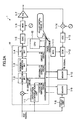
- FIG. 2A is a schematic block diagram of a distortion compensating device 10 applied to a transmitter 1 of a direct RF modulation type
- FIG. 2B is a schematic block diagram of CPU 1-15 shown in FIG. 2A
- the transmitter 1 (or the distortion compensating device 10) includes a distortion compensation unit 1-1, a direct current (DC) correction unit 1-2, an orthogonality correction unit 1-3, an IQ correction unit 1-4, a digital-to-analog converter (DAC) 1-5, and a CPU 1-15.
- DC direct current
- DAC digital-to-analog converter
- the transmitter 1 also includes a quadrature modulator (MOD) 1-6, a power amplifier (PA) 1-7, a delay unit 1-8, memories 1-9 and 1-10, a digital oscillator (NCO) 1-11, a quadrature demodulator (DEM) 1-12, an analog-to-digital converter (ADC) 1-13, and a down converter 1-14.
- MOD quadrature modulator
- PA power amplifier
- PA power amplifier
- delay unit 1-8 memories 1-9 and 1-10
- NCO digital oscillator
- DEM quadrature demodulator
- ADC analog-to-digital converter
- the CPU 1-15 includes a phase adjusting unit 21, a phase adjustment result storing unit 22, a phase adjustment result comparison and determination unit 23, and a correction control unit 24, as illustrated in FIG. 2B.
- the correction control unit 24 has a quadrature modulation correcting instruction generator 25, and a distortion compensation control instruction generator 29.
- the quadrature modulation correcting generator generates, for example, a DC offset correction instruction 26 for controlling the operation of the DC correction unit 1-2, an orthogonality correction instruction 27 for controlling the operation of the orthogonality correction unit 1-3, and an IQ amplitude correction instruction 28 for controlling the operation of the IQ correction unit 1-4.
- a portion of the transmission signal to be output from the power amplifier (PA) 1-7 is branched, and subjected to frequency conversion to an intermediate frequency by the down converter 1-14, which signal is then converted to a digital signal by the analog-to-digital converter (ADC) 1-13.
- the A/D converted signal is subjected to quadrature demodulation by the quadrature demodulator (DEM) 1-12, and stored as a feedback signal (FB) in the memory 1-10.
- a portion of the transmission signal input to the transmitter 1 is also branched and used as a reference signal (Ref).
- the reference signal is delayed at the delay unit 1-8 for a duration corresponding to the feedback time of the feedback signal (FB), and then stored in the memory 1-9.
- the phase adjusting unit 21 of the CPU 1-15 adjusts and sets initial phase ⁇ in the NCO 1-11 for quadrature demodulation of a current feedback signal, based on feedback signal FB and reference signal Ref read from the memories 1-10 and 1-9, respectively.
- the phase adjustment result storing unit 22 stores the phase adjustment result (phase ⁇ ).
- the phase adjustment result comparison and determination unit 23 compares the current phase adjustment result with the previous phase adjustment result stored in the phase adjustment result storing unit 22, and determines whether the comparison result satisfies a prescribed condition (for example, whether the difference between the current and previous phase adjustment results resides in a prescribed range).
- the correction control unit 24 controls distortion compensation and/or correction for quadrature modulation (including DC correction, orthogonality correction, and IQ amplitude correction) based on the comparison result of the current and previous phase adjustment results.
- the CPU 1-15 also determines a distortion compensation weighting factor (or coefficient) for the distortion compensation unit 1-1, based on comparison between the reference signal (Ref) and the feedback signal (FB) read from the memories 1-9 and 1-10, respectively, and supplies the weighting factor (or coefficient) to the distortion compensation unit 1-1.
- the distortion compensation unit 1-1 updates the weighting factor in real time, in response to the receipt of the newly supplied weighting factor, and multiplies the reference signal (Ref) by the updated weighting factor to give an inverted distortion characteristic of the power amp characteristic or other distortion characteristics to the reference signal (transmission signal) in advance. In this manner, distortion due to power amplifier (PA) 1-7 and other components is compensated for.
- the above-described distortion compensation is performed when the CPU 1-15 supplies a distortion compensation instruction, that is, when the phase adjustment comparison result satisfies a prescribed condition.
- the initial phase of the digital oscillator (NCO) 1-11 used for the quadrature demodulator (DEM) 1-12 is adjusted.
- the CPU 1-15 performs arithmetic operations using the reference signal (Ref) data and the feedback signal (FB) data read from the memories 1-9 and 1-10, respectively.
- ⁇ tan ⁇ 1 C real / C imaginary is determined.
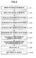
- the phase ⁇ is set as the initial phase of the digital oscillator (NCO) 1-11 used for the quadrature demodulator (DEM) 1-12. This operations flow is illustrated in FIG. 3.
- feedback signal (FB) data are written in memory 1-10 (step 2-1), and reference signal (Ref) data are written in memory 1-9 (step 2-2). All the feedback signal (FB) data items written in the memory 1-10 are read (step 2-3) and integrated (step 2-4). Similarly, all the reference signal (Ref) data items written in the memory 1-9 are read (step 2-5) and integrated (step 2-6).
- step 2-7 and step 2-8, respectively the real part and the imaginary part of the correlation value are calculated (step 2-7 and step 2-8, respectively) using equation (4), and a phase ⁇ is calculated from the real part and the imaginary part of the correlation value (step 2-9).
- the determined phase ⁇ is set as the initial phase of the digital oscillator (NCO) 1-11.
- FIG. 4A and FIG. 4B are diagrams showing direct current (DC) offset correction.
- the DC correction unit 1-2 has a first adder 3a-1 for adding an in-phase (Ich) correction value to the in-phase (Ich) component, and a second adder 3a-2 for adding a quadrature (Qch) correction value to the quadrature (Qch) component.
- Ref Ref_ich + j ⁇ Ref_qch
- FB FB_ich + j ⁇ FB_qch
- FIG. 4B(1) and FIG. 4B(2) illustrate a reference signal (Ref) vector and a phase-adjusted feedback signal (FB) vector, respectively.
- the reference signal (Ref) vector does not contain direct current (DC) offset component
- the phase-adjusted feedback signal (FB) contains a direct current (DC) vector component generated by the quadrature modulator (MOD) 1-6 and/or other elements.
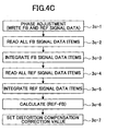
- FIG. 4C is an operations flow of direct current (DC) offset correction.
- the current feedback signal (FB) is subjected to phase adjustment and written in the memory 1-10 (step 3c-1). Then, all the feedback signal (FB) data items are read from the memory 1-10 (step 3c-2) and integrated (step 3c-3).
- All the reference signal (Ref) data items are also read from the memory 1-9 (step 3c-4) and integrated (step 3c-5).
- the reference signal (Ref) data have also been written in the memory 1-9 in the step of phase adjustment.
- a correction vector is calculated by subtracting the integrated feedback signal (FB) from the integrated reference signal (Ref) (step 3c-6), and the calculated correction vector is set as the direct current (DC) correction value (step 3c-7).
- An output signal from the quadrature modulator (MOD) 1-6 contains deviation from orthogonality, and is expressed as I ⁇ cos ⁇ ⁇ t + Q ⁇ sin ⁇ ⁇ t + ⁇ where ⁇ denotes an angular frequency of quadrature modulation, ⁇ denotes the deviation angle from orthogonality, I denotes the in-phase component of the input signal, and Q denotes the quadrature component of the input signal.
- This output signal is fed back to the quadrature demodulator (DEM) 1-12, and an arithmetic operation expressed as I ⁇ cos ⁇ ⁇ t + Q ⁇ sin ⁇ ⁇ t + ⁇ ⁇ cos ⁇ ⁇ t + j ⁇ sin ⁇ ⁇ t is carried out on the feedback signal when it is quadrature demodulated and converted to a baseband signal.
- DEM quadrature demodulator
- Deviation angle ⁇ from orthogonality is determined in the following process.
- Ref Ref_ich + j ⁇ Ref_qch
- FB FB_ich + j ⁇ FB_qch
- FIG. 5A illustrates an example of the orthogonality correction unit 1-3
- FIG. 5B illustrates an operations flow of the orthogonality correction process.
- the orthogonality correction unit 1-3 has a tangent table 4a-1 for acquiring tan ⁇ and a secant (1/cos) table 4a-2 for acquiring (1/cos ⁇ ) of the deviation angle ⁇ from orthogonality.
- parameters I' and Q' with the orthogonality corrected are output.
- the current feedback signal (FB) is subjected to phase adjustment and written in the memory 1-10 (step 4b-1).
- a feedback signal (FB) data item is read from the memory 1-10 (step 4b-2), and a power level Pow-FB of this feedback signal (FB) is calculated (step 4b-3).
- a reference signal (Ref) data item is read from the memory 1-9 (step 4b-4), and a power level Pow-Ref of this reference signal (Ref) is calculated (step 4b-5).
- the current reference signal (Ref) data item has been written in the memory 1-9 in the step of phase adjustment.
- step 4b-6 the product (Ref_ich)(Ref_qch) of the real part and the imaginary part of the reference signal is calculated (step 4b-6).
- the steps 4b-2 through 4b-6 are repeated until all the feedback signal (FB) data items and the reference signal (Ref) data items are processed (step 4b-7).
- step 4b-7 When all the data items have been processed (YES in step 4b-7), the power levels Pow_FB of all the feedback signal data items are integrated and averaged (step 4b-8). Similarly, the power levels Pow_Ref of all the reference signal data items are integrated and averaged (step 4b-9). The products (Ref_ich) (Ref_qch) of all the reference signal data items are also integrated and averaged (step 4b-10).
- a deviation angle ⁇ from orthogonality is calculated using Equation (18) (step 4b-11). This deviation angle ⁇ is used as the orthogonality correction value (step 4b-12).
- Errors in amplitudes of in-phase component (I) and quadrature component (Q) are determined by (FB_Bal)-(Ref_Bal), and the amplitudes of the in-phase component (I) and the quadrature component (Q) are corrected based on the determined error.
- FIG. 6A illustrates an example of the IQ correction unit 1-4
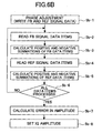
- FIG. 6B illustrates an operations flow of the IQ correction process.
- the IQ correction unit 1-4 is configured to multiply the in-phase component (I) and the quadrature component (Q) by the in-phase (Ich) correction value and the quadrature (Qch) correction value, respectively.
- the current feedback signal (FB) is subjected to phase adjustment and written in the memory 1-10 (step 5b-1).
- Feedback signal (FB) data items are read from the memory 1-10 (step 5b-2), and a positive summation (i.e., the summation of all the positive feedback signal data values) and a negative summation (i.e., the summation of all the negative feedback signal data values) are determined (step 5b-3).
- Reference signal (FB) data items are also read from the memory 1-9 (step 5b-4), and a positive summation (i.e., the summation of all the positive reference signal data values) and a negative summation (i.e., the summation of all the negative reference signal data values) are determined (step 5b-5).
- the steps 5b-2 through 5b-5 are repeated until all the feedback signal (FB) data items and the reference signal (Ref) data items (step 4b-7) are processed.
- step 5b-6 When all the data items have been processed (YES in step 5b-6), an error in amplitude is calculated from the mean absolute FB_Bal of the feedback signals and the mean absolute Ref_Bal of the reference signals (step 5b-7). Based on the calculated error, amplitude correction values for the in-phase component (I) and the quadrature component (Q) of the input signal (transmission signal) are determined (step 5b-8).
- the above described distortion compensation and correction for quadrature modulation are performed only when a phase adjustment value (i.e., a phase difference between the feedback signal and the reference signal) is correctly determined because, with an incorrect phase adjustment value, distortion compensation and/or correction for quadrature modulation cannot be correctly performed.
- a phase adjustment value i.e., a phase difference between the feedback signal and the reference signal
- phase difference between the feedback signal and the reference signal resides in a correct range based on determination as to whether the current phase adjustment result is within an acceptable error range with respect to the previous phase adjustment results.
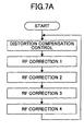
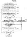
- FIG. 7A, FIG. 7B, and FIG. 8 are flowcharts of distortion compensation control and quadrature modulation correction control.
- distortion compensation various types of RF quadrature modulation corrections e.g., RF correction 1 through RF correction 4
- the CPU 1-5 as illustrated in FIG. 7A, using a prescribed criterion as to the appropriateness of the phase adjustment performed on the feedback signal.
- FIG. 7B is a sub-routine of any one of RF correction controls for quadrature modulation.
- a target correction counts value (or the number of corrections) is set to a prescribed value K (step 7-1), and a successful phase adjustment counts value (i.e., the number of phase adjustments performed with correct phase values) is set to zero for initialization (step 7-2).
- the previous phase adjustment result (phase adjusting value ⁇ ) is read from the phase adjustment result storing unit 22 shown in FIG. 2B (step 7-3), while a current phase adjustment result (phase adjusting value ⁇ ') is acquired by the phase adjusting unit 21 (step 7-4).
- the current phase adjusting value ⁇ ' is compared with the previous phase adjusting value ⁇ and it is determined by the phase adjustment comparison and determination unit 23 whether the difference ⁇ '- ⁇ between the current and previous phase adjustment results is within the range from -N° to N° (step 7-5).
- step 7-5 If the difference between the current phase adjusting value ⁇ ' and the previous phase adjusting value ⁇ is within the range from -N° to N° (YES in step 7-5), the successful phase adjustment counts value is incremented (step 7-6). If the current phase adjustment result differs from the previous phase adjustment result by an amount that exceeds the ⁇ N range (NO in step 7-5), the successful phase adjustment counts value is maintained at zero (step 7-7), and the process jumps to step 7-10 described below.
- step 7-8 After incrementing of the successful phase adjustment counts value, it is determined by the phase adjustment result comparison and determination unit 23 whether the successful phase adjustment counts value is at or above a prescribed value "m" (step 7-8). If the successful phase adjustment counts value is not greater than "m" (NO in step 7-8), the process jumps to step 7-10 without performing RF correction.
- the correction control unit 24 If the successful phase adjustment counts value is greater than "m" (YES in step 7-8), the correction control unit 24 generates an instruction for RF correction (for example, an instruction for DC offset correction) to cause the associated element or functional block to perform this RF correction, and the correction counts value is incremented (step 7-9). Then, it is determined whether the RF correction has been performed at least K times (step 7-10). If the correction counts value does not reach K (NO in step 7-10), the process returns to step 7-3 to repeat the process until the RF correction has been performed at least K times.
- RF correction for example, an instruction for DC offset correction
- step 7-10 If the correction counts value reaches K (YES in step 7-10), the sub-routine finishes, and the process returns to the main flow shown in FIG. 7A to perform next RF correction control.
- phase adjustment result ( ⁇ ) is within the correct range at least a prescribed number (m) of times
- RF correction is performed and this RF correction process is repeated until the RF correction is performed at least a target number of times (K times).
- N is an acceptable phase error
- m and K are natural numbers.
- FIG. 8 is a flowchart of the sub-routine of distortion compensation control shown in FIG. 7A.
- the previous phase adjustment result phase adjusting value ⁇
- a current phase adjustment result phase adjusting value ⁇ '
- the current phase adjusting value ⁇ ' is compared with the previous phase adjusting value ⁇ and it is determined by the phase adjustment comparison and determination unit 23 whether the difference ⁇ '- ⁇ between the current and previous phase adjustment results is within the range from -N° to N° (step 8-4).
- the correction control unit 24 allows distortion compensation to be performed (step 8-5), and determines whether the current timing is in the distortion compensation period (step 8-6). The distortion compensation is performed until the end of the distortion compensation period. If the current timing is out of the distortion compensation period (NO in step 8-6), distortion compensation is not performed (step 8-7).
Landscapes
- Engineering & Computer Science (AREA)
- Computer Networks & Wireless Communication (AREA)
- Signal Processing (AREA)
- Physics & Mathematics (AREA)
- Nonlinear Science (AREA)
- Power Engineering (AREA)
- Digital Transmission Methods That Use Modulated Carrier Waves (AREA)
- Transmitters (AREA)
- Amplifiers (AREA)
Abstract
Description
- The present invention generally relates to distortion compensation, and more particularly, to a distortion compensation technique applied to a transmitter for transmitting quadrature modulated signals in wireless digital communication systems.
- In mobile communications, including IMT-2000, broadband radio services are being offered, and especially, broader-band radio transmission is being discussed for the next-generation mobile communication schemes. In general, complex baseband signals are first converted to an intermediate frequency (IF) band, and the IF signals are further converted to radio frequency (RF) signals suitable for broadband radio transmission.
- Such broadband mobile communication systems require bandpass filters to have steep filter characteristics, as well as a flat characteristic over the entire passband, in order to sufficiently reduce high-frequency components generated during the frequency conversion. However, since sophisticated and high-performance devices and circuits are required in broadband radio transmission, the device scale and the manufacturing cost increase consequently. To avoid this inconvenience, direct RF modulation schemes for converting baseband signals directly to RF signals are attracting attentions.
- Meanwhile, in recent years and continuing, highly efficiency digital transmission schemes are widely employed in wireless communication systems. When employing a multi-level phase modulation scheme known as one of the high efficiency transmission schemes, a technique for reducing non-linear distortion in a power amplifier and adjacent channel leakage at a transmission end is required to improve power efficiency. This technique, known as distortion compensation, is an adaptive predistortion type for a transmission amplifier.
- With a distortion compensating transmission amp of an adaptive predistortion type, a portion of the output signal (quadrature modulated signal) of the transmitter is subjected to quadrature demodulation to produce a feedback signal, and the feedback signal is compared with a transmission signal (reference signal) prior to quadrature modulation. Based on the comparison result, a weighting factor for distortion compensation is updated in real time. The transmission signal (reference signal) is multiplied by the updated weighting factor in order to give an inverted characteristic to the transmission signal in advance, and then quadrature modulation and power amplification are performed on the distortion compensated transmission signal. After the quadrature modulation and power amplification, the transmission signal is finally transmitted from the transmitter. See, for example, International Patent Publication
WO 03/103163 - However, with such a direct RF modulation scheme, errors are generated in both the in-phase component and the quadrature component of the transmission signal to be supplied to the quadrature modulator, due to variation in analog devices and change over time. As a result, undesirable leakage of waves is generated as imaginary components in the modulated analog transmission signals, which causes degradation of the transmission signal quality.
- In addition, the transmission signal (reference signal) is delayed using a delay element in the comparison process with the feedback signal in order to make the phases of the transmissions signal and the feed back signal be consistent with each other. Even if the delay time is correctly set in the delay element, the phase of the feedback signal itself fluctuates due to clock jitter caused by thermal noise or external disturbance. In short, it is difficult for a conventional adaptive predistortion technique to guarantee stable and reliable distortion compensation, which technique is likely to generate undesirable out-of-band power radiation.
- Another publication, Japanese Patent Application Laid-open (Kokai)
No. 6-37831A - However, due to malfunction of analog circuits, including an oscillator for a down converter, the phase difference between the reference signal and the feedback signal may not be correctly determined. In this case, distortion compensation and/or other corrections cannot be performed correctly, causing abnormal operations.
- FIG. 1 is a diagram illustrating phase adjustment results performed in normal operation and abnormal operation of the oscillator for a down converter. In the normal operation, the phase is set to substantially 90 degrees to maintain orthogonality. In contrast, during malfunctioning of the oscillator, the phase varies randomly ranging from -180° to 180° even after the phase adjustment.
- The present invention is conceived in view of the above-described problems in the prior art, and it is an object of the invention to provide a distortion compensation technique that allows a transmitter to transmit a high-quality distortion-compensated and quadrature modulated signal, without causing undesirable leakage of out-of-band radiation.
- In a preferred embodiment, it is determined whether the phase difference between the feedback signal and the reference signal reside in a normal range, and if the phase difference is in the normal range, distortion compensation and/or other corrections for quadrature modulation are performed.
- In one aspect of the invention, a distortion compensating device applied to a transmitter for transmitting a quadrature modulated signal in a wireless digital communication system is provided. The distortion compensating device includes:
- (a) a phase adjusting unit configured to determine a phase adjustment value for a feedback signal subjected to quadrature demodulation, based on comparison between the feedback signal and a reference signal to be transmitted from the transmitter;
- (b) a phase adjustment result storing unit configured to store a current phase adjustment result representing the determined phase adjustment value;
- (c) a phase adjustment result comparison and determination unit configured to compare a current phase adjustment result with a previous phase adjustment result; and
- (d) a correction control unit configured to allow correction for quadrature modulation to be performed if the phase adjustment comparison result satisfies a prescribed condition.
- In a preferred example, correction for quadrature modulation is performed if the phase adjustment comparison result satisfies the prescribed condition at least a prescribed number of times.
- Examples of correction for quadrature modulation include direct current (DC) offset correction, orthogonality correction, and amplitude correction performed on the in-phase component and the quadrature component of the reference signal.
- In another preferred example, distortion compensation is performed if the difference between the current phase adjustment result and the previous phase adjustment result is within a prescribed range.
- In another aspect of the invention, a distortion compensating method applied to a transmitter for transmitting a quadrature modulated signal in a wireless digital communication system is provided. This method includes the steps of:
- (a) determining a current phase adjustment value for a feedback signal subjected to quadrature demodulation, based on comparison between the feedback signal and a reference signal to be transmitted from the transmitter;
- (b) comparing the current phase adjustment value with a previous phase adjustment value; and
- (c) allowing correction for quadrature modulation to be performed if the current phase adjustment value resides in an acceptable error range with respect to the previous phase adjustment value at least a prescribed number of times.
- Other objects, features, and advantages of the present invention will become more apparent from the following detailed description when read in conjunction with the accompanying drawings, in which:
- FIG. 1 is a diagram illustrating phase adjustment results in normal operation and abnormal operation;
- FIG. 2A is a schematic block diagram of a distortion compensating device applied to a transmitter, and FIG. 2B is a functional block diagram of the CPU used in the distortion compensating device shown in FIG. 2A;
- FIG. 3 is a flowchart of the phase adjustment operations for setting a phase adjustment value θ for a feedback signal;
- FIG. 4A and FIG. 4B are schematic diagrams for explaining direct current (DC) offset correction, and FIG. 4C is a flowchart of DC offset correction;
- FIG. 5A is a schematic circuit diagram for explaining orthogonality correction, and FIG. 5B is a flowchart of operations for orthogonality correction;
- FIG. 6A is a schematic diagram for explaining amplitude correction for the in-phase component (I) and the quadrature component (Q) of the input signal, and FIG. 6B is a flowchart of operations for IQ amplitude correction;
- FIG. 7A is an outlined operations flow of the distortion compensation, and FIG. 7B is a detailed operations flow of correction control for direct RF type quadrature modulation according to an embodiment of the invention; and
- FIG. 8 is a detailed operations flow of distortion compensation control according to an embodiment of the invention.
- FIG. 2A is a schematic block diagram of a
distortion compensating device 10 applied to atransmitter 1 of a direct RF modulation type, and FIG. 2B is a schematic block diagram of CPU 1-15 shown in FIG. 2A. The transmitter 1 (or the distortion compensating device 10) includes a distortion compensation unit 1-1, a direct current (DC) correction unit 1-2, an orthogonality correction unit 1-3, an IQ correction unit 1-4, a digital-to-analog converter (DAC) 1-5, and a CPU 1-15. Thetransmitter 1 also includes a quadrature modulator (MOD) 1-6, a power amplifier (PA) 1-7, a delay unit 1-8, memories 1-9 and 1-10, a digital oscillator (NCO) 1-11, a quadrature demodulator (DEM) 1-12, an analog-to-digital converter (ADC) 1-13, and a down converter 1-14. - The CPU 1-15 includes a
phase adjusting unit 21, a phase adjustmentresult storing unit 22, a phase adjustment result comparison anddetermination unit 23, and acorrection control unit 24, as illustrated in FIG. 2B. Thecorrection control unit 24 has a quadrature modulation correctinginstruction generator 25, and a distortion compensationcontrol instruction generator 29. The quadrature modulation correcting generator generates, for example, a DC offsetcorrection instruction 26 for controlling the operation of the DC correction unit 1-2, anorthogonality correction instruction 27 for controlling the operation of the orthogonality correction unit 1-3, and an IQamplitude correction instruction 28 for controlling the operation of the IQ correction unit 1-4. - A portion of the transmission signal to be output from the power amplifier (PA) 1-7 is branched, and subjected to frequency conversion to an intermediate frequency by the down converter 1-14, which signal is then converted to a digital signal by the analog-to-digital converter (ADC) 1-13. The A/D converted signal is subjected to quadrature demodulation by the quadrature demodulator (DEM) 1-12, and stored as a feedback signal (FB) in the memory 1-10.
- A portion of the transmission signal input to the
transmitter 1 is also branched and used as a reference signal (Ref). The reference signal is delayed at the delay unit 1-8 for a duration corresponding to the feedback time of the feedback signal (FB), and then stored in the memory 1-9. - The
phase adjusting unit 21 of the CPU 1-15 adjusts and sets initial phase θ in the NCO 1-11 for quadrature demodulation of a current feedback signal, based on feedback signal FB and reference signal Ref read from the memories 1-10 and 1-9, respectively. The phase adjustmentresult storing unit 22 stores the phase adjustment result (phase θ). The phase adjustment result comparison anddetermination unit 23 compares the current phase adjustment result with the previous phase adjustment result stored in the phase adjustmentresult storing unit 22, and determines whether the comparison result satisfies a prescribed condition (for example, whether the difference between the current and previous phase adjustment results resides in a prescribed range). Thecorrection control unit 24 controls distortion compensation and/or correction for quadrature modulation (including DC correction, orthogonality correction, and IQ amplitude correction) based on the comparison result of the current and previous phase adjustment results. - Returning to FIG. 2A, the CPU 1-15 also determines a distortion compensation weighting factor (or coefficient) for the distortion compensation unit 1-1, based on comparison between the reference signal (Ref) and the feedback signal (FB) read from the memories 1-9 and 1-10, respectively, and supplies the weighting factor (or coefficient) to the distortion compensation unit 1-1. The distortion compensation unit 1-1 updates the weighting factor in real time, in response to the receipt of the newly supplied weighting factor, and multiplies the reference signal (Ref) by the updated weighting factor to give an inverted distortion characteristic of the power amp characteristic or other distortion characteristics to the reference signal (transmission signal) in advance. In this manner, distortion due to power amplifier (PA) 1-7 and other components is compensated for.
- The above-described distortion compensation is performed when the CPU 1-15 supplies a distortion compensation instruction, that is, when the phase adjustment comparison result satisfies a prescribed condition.
- Next, adjustment of the initial phase θ is explained below. To deal with the phase fluctuation of the feedback signal (FB), the initial phase of the digital oscillator (NCO) 1-11 used for the quadrature demodulator (DEM) 1-12 is adjusted.
- The CPU 1-15 performs arithmetic operations using the reference signal (Ref) data and the feedback signal (FB) data read from the memories 1-9 and 1-10, respectively. Reference signal (Ref) and the feedback signal (FB) are expressed as


where Ref denotes a reference signal, Ref_ich denotes the in-phase component of the reference signal, Ref_qch denotes the quadrature component of the reference signal, FB denotes a feedback signal, FB_ich denotes the in-phase component of the feedback signal, and FB_qch denotes the quadrature component of the feedback signal. - A correlation value C is calculated by

- If FB=Ref×Aexp(-jθ) holds, the correlation value C is also expressed as

- From exp(jθ)=cosθ+jsinθ, the real part and the imaginary part of the correlation value are expressed as


- Based on the correlation result,

- First, feedback signal (FB) data are written in memory 1-10 (step 2-1), and reference signal (Ref) data are written in memory 1-9 (step 2-2). All the feedback signal (FB) data items written in the memory 1-10 are read (step 2-3) and integrated (step 2-4). Similarly, all the reference signal (Ref) data items written in the memory 1-9 are read (step 2-5) and integrated (step 2-6).
- Then, the real part and the imaginary part of the correlation value are calculated (step 2-7 and step 2-8, respectively) using equation (4), and a phase θ is calculated from the real part and the imaginary part of the correlation value (step 2-9). The determined phase θ is set as the initial phase of the digital oscillator (NCO) 1-11.
- Next, explanation is made of DC offset correction carried out by the DC correction unit 1-2.
- FIG. 4A and FIG. 4B are diagrams showing direct current (DC) offset correction. As illustrated in FIG. 4A, the DC correction unit 1-2 has a
first adder 3a-1 for adding an in-phase (Ich) correction value to the in-phase (Ich) component, and asecond adder 3a-2 for adding a quadrature (Qch) correction value to the quadrature (Qch) component. - Using the reference signal (Ref) and the phase-adjusted feedback signal (FB), which signals are expressed as


- FIG. 4B(1) and FIG. 4B(2) illustrate a reference signal (Ref) vector and a phase-adjusted feedback signal (FB) vector, respectively. The reference signal (Ref) vector does not contain direct current (DC) offset component, while the phase-adjusted feedback signal (FB) contains a direct current (DC) vector component generated by the quadrature modulator (MOD) 1-6 and/or other elements.
- FIG. 4C is an operations flow of direct current (DC) offset correction. The current feedback signal (FB) is subjected to phase adjustment and written in the memory 1-10 (step 3c-1). Then, all the feedback signal (FB) data items are read from the memory 1-10 (step 3c-2) and integrated (step 3c-3).
- All the reference signal (Ref) data items are also read from the memory 1-9 (step 3c-4) and integrated (step 3c-5). The reference signal (Ref) data have also been written in the memory 1-9 in the step of phase adjustment. A correction vector is calculated by subtracting the integrated feedback signal (FB) from the integrated reference signal (Ref) (step 3c-6), and the calculated correction vector is set as the direct current (DC) correction value (step 3c-7).
- Next, explanation is made of orthogonality correction carried out by the orthogonality correction unit 1-3. An output signal from the quadrature modulator (MOD) 1-6 contains deviation from orthogonality, and is expressed as

where ω denotes an angular frequency of quadrature modulation, φ denotes the deviation angle from orthogonality, I denotes the in-phase component of the input signal, and Q denotes the quadrature component of the input signal. - This output signal is fed back to the quadrature demodulator (DEM) 1-12, and an arithmetic operation expressed as

- The real part of equation (7) becomes


- The imaginary part of equation (7) becomes


- Deviation angle φ from orthogonality is determined in the following process. Using the reference signal (Ref) and the feedback signal (FB) expressed as


- If the feedback signal (FB) contains phase rotation of θ and deviation angle φ from orthogonality, then the feed back signal (FB) is expressed as


- From the foregoing description, the deviation angle φ from orthogonality is expressed as

- FIG. 5A illustrates an example of the orthogonality correction unit 1-3, and FIG. 5B illustrates an operations flow of the orthogonality correction process. The orthogonality correction unit 1-3 is configured to perform the above-described arithmetic operations, which are represented by


- In the operation flow shown in FIG. 5B, the current feedback signal (FB) is subjected to phase adjustment and written in the memory 1-10 (
step 4b-1). A feedback signal (FB) data item is read from the memory 1-10 (step 4b-2), and a power level Pow-FB of this feedback signal (FB) is calculated (step 4b-3). - Then, a reference signal (Ref) data item is read from the memory 1-9 (
step 4b-4), and a power level Pow-Ref of this reference signal (Ref) is calculated (step 4b-5). The current reference signal (Ref) data item has been written in the memory 1-9 in the step of phase adjustment. - Then, the product (Ref_ich)(Ref_qch) of the real part and the imaginary part of the reference signal is calculated (
step 4b-6). Thesteps 4b-2 through 4b-6 are repeated until all the feedback signal (FB) data items and the reference signal (Ref) data items are processed (step 4b-7). - When all the data items have been processed (YES in
step 4b-7), the power levels Pow_FB of all the feedback signal data items are integrated and averaged (step 4b-8). Similarly, the power levels Pow_Ref of all the reference signal data items are integrated and averaged (step 4b-9). The products (Ref_ich) (Ref_qch) of all the reference signal data items are also integrated and averaged (step 4b-10). - Based on the feedback signal average power level Pow_FB, the reference signal average power level Pow_Ref, and the average product (Ref_ich)(Ref_qch) of the real part and the imaginary part of the reference signal, a deviation angle φ from orthogonality is calculated using Equation (18) (
step 4b-11). This deviation angle φ is used as the orthogonality correction value (step 4b-12). - Next, explanation is made of amplitude correction for the in-phase component (I) and the quadrature component (Q) carried out by the IQ correction unit 1-4. If the cumulative value of the reference signals is expressed as Ref_Acm=ΣRef, and if the cumulative value of the feedback signals is expressed as FB_Acm=ΣFB, the mean absolute value of the reference signal Ref_Bal and the mean absolute value of the feedback signal FB_Bal are expressed, respectively, as


- Errors in amplitudes of in-phase component (I) and quadrature component (Q) are determined by (FB_Bal)-(Ref_Bal), and the amplitudes of the in-phase component (I) and the quadrature component (Q) are corrected based on the determined error.
- FIG. 6A illustrates an example of the IQ correction unit 1-4, and FIG. 6B illustrates an operations flow of the IQ correction process. The IQ correction unit 1-4 is configured to multiply the in-phase component (I) and the quadrature component (Q) by the in-phase (Ich) correction value and the quadrature (Qch) correction value, respectively.
- In operations shown in FIG. 6B, the current feedback signal (FB) is subjected to phase adjustment and written in the memory 1-10 (
step 5b-1). Feedback signal (FB) data items are read from the memory 1-10 (step 5b-2), and a positive summation (i.e., the summation of all the positive feedback signal data values) and a negative summation (i.e., the summation of all the negative feedback signal data values) are determined (step 5b-3). - Reference signal (FB) data items are also read from the memory 1-9 (
step 5b-4), and a positive summation (i.e., the summation of all the positive reference signal data values) and a negative summation (i.e., the summation of all the negative reference signal data values) are determined (step 5b-5). Thesteps 5b-2 through 5b-5 are repeated until all the feedback signal (FB) data items and the reference signal (Ref) data items (step 4b-7) are processed. - When all the data items have been processed (YES in
step 5b-6), an error in amplitude is calculated from the mean absolute FB_Bal of the feedback signals and the mean absolute Ref_Bal of the reference signals (step 5b-7). Based on the calculated error, amplitude correction values for the in-phase component (I) and the quadrature component (Q) of the input signal (transmission signal) are determined (step 5b-8). - In the embodiment, the above described distortion compensation and correction for quadrature modulation (including DC offset correction, orthogonality correction, and IQ amplitude correction) are performed only when a phase adjustment value (i.e., a phase difference between the feedback signal and the reference signal) is correctly determined because, with an incorrect phase adjustment value, distortion compensation and/or correction for quadrature modulation cannot be correctly performed.
- To realize this, it is determined whether the phase difference between the feedback signal and the reference signal resides in a correct range based on determination as to whether the current phase adjustment result is within an acceptable error range with respect to the previous phase adjustment results.
- FIG. 7A, FIG. 7B, and FIG. 8 are flowcharts of distortion compensation control and quadrature modulation correction control. With the
distortion compensating device 10 shown in FIG. 2A and FIG. 2B, distortion compensation various types of RF quadrature modulation corrections (e.g.,RF correction 1 through RF correction 4) are controlled by the CPU 1-5, as illustrated in FIG. 7A, using a prescribed criterion as to the appropriateness of the phase adjustment performed on the feedback signal. - FIG. 7B is a sub-routine of any one of RF correction controls for quadrature modulation. In the example shown in FIG. 7B, a target correction counts value (or the number of corrections) is set to a prescribed value K (step 7-1), and a successful phase adjustment counts value (i.e., the number of phase adjustments performed with correct phase values) is set to zero for initialization (step 7-2).
- Then, the previous phase adjustment result (phase adjusting value θ) is read from the phase adjustment
result storing unit 22 shown in FIG. 2B (step 7-3), while a current phase adjustment result (phase adjusting value θ') is acquired by the phase adjusting unit 21 (step 7-4). The current phase adjusting value θ' is compared with the previous phase adjusting value θ and it is determined by the phase adjustment comparison anddetermination unit 23 whether the difference θ'-θ between the current and previous phase adjustment results is within the range from -N° to N° (step 7-5). - If the difference between the current phase adjusting value θ' and the previous phase adjusting value θ is within the range from -N° to N° (YES in step 7-5), the successful phase adjustment counts value is incremented (step 7-6). If the current phase adjustment result differs from the previous phase adjustment result by an amount that exceeds the ±N range (NO in step 7-5), the successful phase adjustment counts value is maintained at zero (step 7-7), and the process jumps to step 7-10 described below.
- After incrementing of the successful phase adjustment counts value, it is determined by the phase adjustment result comparison and
determination unit 23 whether the successful phase adjustment counts value is at or above a prescribed value "m" (step 7-8). If the successful phase adjustment counts value is not greater than "m" (NO in step 7-8), the process jumps to step 7-10 without performing RF correction. - If the successful phase adjustment counts value is greater than "m" (YES in step 7-8), the
correction control unit 24 generates an instruction for RF correction (for example, an instruction for DC offset correction) to cause the associated element or functional block to perform this RF correction, and the correction counts value is incremented (step 7-9). Then, it is determined whether the RF correction has been performed at least K times (step 7-10). If the correction counts value does not reach K (NO in step 7-10), the process returns to step 7-3 to repeat the process until the RF correction has been performed at least K times. - If the correction counts value reaches K (YES in step 7-10), the sub-routine finishes, and the process returns to the main flow shown in FIG. 7A to perform next RF correction control.
- In this manner, if the phase adjustment result (θ) is within the correct range at least a prescribed number (m) of times, RF correction is performed and this RF correction process is repeated until the RF correction is performed at least a target number of times (K times). In the operations flow, N is an acceptable phase error, and m and K are natural numbers.
- FIG. 8 is a flowchart of the sub-routine of distortion compensation control shown in FIG. 7A. When distortion compensation control is started (step 8-1), the previous phase adjustment result (phase adjusting value θ) is read from the phase adjustment
result storing unit 22 shown in FIG. 2B (step 8-2), while a current phase adjustment result (phase adjusting value θ') is acquired by the phase adjusting unit 21 (step 8-3). The current phase adjusting value θ' is compared with the previous phase adjusting value θ and it is determined by the phase adjustment comparison anddetermination unit 23 whether the difference θ'-θ between the current and previous phase adjustment results is within the range from -N° to N° (step 8-4). - If the difference between the current phase adjusting value θ' and the previous phase adjusting value θ is within the range from -N° to N° (YES in step 8-4), the
correction control unit 24 allows distortion compensation to be performed (step 8-5), and determines whether the current timing is in the distortion compensation period (step 8-6). The distortion compensation is performed until the end of the distortion compensation period. If the current timing is out of the distortion compensation period (NO in step 8-6), distortion compensation is not performed (step 8-7). - In this manner, appropriateness of performing distortion compensation is determined based on whether the comparison result of the current and previous phase adjustment results satisfies a prescribed condition.
- With this arrangement, abnormal operation of distortion compensation and/or RF correction for quadrature modulation due to malfunction of an oscillator for the down converter and other elements in an analog section can be prevented.
- Because distortion compensation and/or correction for quadrature modulation are performed only when the phase adjustment values are correctly set, undesirable out-of-band radiation can be reduced from the output signal from the transmitter.
Claims (10)
- A distortion compensating device applied to a transmitter for transmitting a quadrature modulated signal in a wireless digital communication system, thee distortion compensating device comprising:a phase adjusting unit configured to determine a phase adjustment value for a feedback signal subjected to quadrature demodulation, based on comparison between the feedback signal and a reference signal to be transmitted from the transmitter;a phase adjustment result storing unit configured to store a current phase adjustment result representing the determined phase adjustment value;a phase adjustment result comparison and determination unit configured to compare the current phase adjustment result with a previous phase adjustment result; anda correction control unit configured to allow correction for quadrature modulation to be performed if the phase adjustment comparison result satisfies a prescribed condition.
- The distortion compensating device of claim 1, wherein the correction control unit allows the correction for quadrature modulation to be performed if the current phase adjustment result is within an acceptable error range with respect to the previous phase adjustment result at least a prescribed number of times.
- The distortion compensating device of claim 1, wherein the correction control unit generates an instruction for performing direct current offset correction on an in-phase component and a quadrature component of the reference signal if the current phase adjustment result is within an acceptable error range with respect to the previous phase adjustment result at least a prescribed number of times.
- The distortion compensating device of claim 1, wherein the correction control unit generates an instruction for performing orthogonality correction on an in-phase component and a quadrature component of the reference signal if the current phase adjustment result is within an acceptable error range with respect to the previous phase adjustment result at least a prescribed number of times.
- The distortion compensating device of claim 1, wherein the correction control unit generates an instruction for performing amplitude correction on an in-phase component and a quadrature component of the reference signal if the current phase adjustment result is within an acceptable error range with respect to the previous phase adjustment result at least a prescribed number of times.
- The distortion compensating device of claim 1, wherein the correction control unit allows distortion compensation to be performed if the difference between the current phase adjustment result and the previous phase adjustment result resides in a prescribed range.
- A distortion compensating method applied to a transmitter for transmitting a quadrature modulated signal in a wireless digital communication system, the method comprising the steps of:determining a current phase adjustment value for a feedback signal subjected to quadrature demodulation, based on comparison between the feedback signal and a reference signal to be transmitted from the transmitter;comparing the current phase adjustment value with a previous phase adjustment value; andallowing correction for quadrature modulation to be performed if the current phase adjustment value resides in an acceptable error range with respect to the previous phase adjustment value at least a prescribed number of times.
- The distortion compensating method of claim 7, wherein at least one of direct current offset correction, orthogonality correction, and amplitude correction for an in-phase component and a quadrature component of the reference signal are performed if the current phase adjustment value resides in the acceptable error range with respect to the previous phase adjustment value at least a prescribed number of times.
- The distortion compensating method of claim 7, further comprising the step of:allowing distortion compensation to be performed on the reference signal if the current phase adjustment value resides in the acceptable error range with respect to the previous phase adjustment value at least a prescribed number of times.
- The distortion compensation method of claim 7, further comprising the step of:performing the correction for quadrature modulation on the reference signal repeatedly a target number of times.
Applications Claiming Priority (1)
| Application Number | Priority Date | Filing Date | Title |
|---|---|---|---|
| JP2005236814A JP4299819B2 (en) | 2005-08-17 | 2005-08-17 | Distortion compensation apparatus and distortion compensation method |
Publications (3)
| Publication Number | Publication Date |
|---|---|
| EP1755302A2 true EP1755302A2 (en) | 2007-02-21 |
| EP1755302A3 EP1755302A3 (en) | 2007-09-12 |
| EP1755302B1 EP1755302B1 (en) | 2009-02-18 |
Family
ID=37433686
Family Applications (1)
| Application Number | Title | Priority Date | Filing Date |
|---|---|---|---|
| EP05258020A Expired - Lifetime EP1755302B1 (en) | 2005-08-17 | 2005-12-23 | Distortion compensation in wireless digital transmitters |
Country Status (4)
| Country | Link |
|---|---|
| US (1) | US7688914B2 (en) |
| EP (1) | EP1755302B1 (en) |
| JP (1) | JP4299819B2 (en) |
| DE (1) | DE602005012819D1 (en) |
Cited By (2)
| Publication number | Priority date | Publication date | Assignee | Title |
|---|---|---|---|---|
| EP2148486A1 (en) * | 2008-07-25 | 2010-01-27 | STMicroelectronics N.V. | Method and system for processing imperfections of a radiofrequency transmission chain and communication device incorporating such a transmission channel. |
| US7688914B2 (en) * | 2005-08-17 | 2010-03-30 | Fujitsu Limited | Distortion compensation in wireless digital communication |
Families Citing this family (8)
| Publication number | Priority date | Publication date | Assignee | Title |
|---|---|---|---|---|
| US7606539B2 (en) * | 2006-08-07 | 2009-10-20 | Infineon Technologies Ag | Adaptive predistorter coupled to a nonlinear element |
| EP2194684B1 (en) | 2007-09-26 | 2012-12-19 | Fujitsu Limited | Transmitter-receiver amplifier and method for compensating delay deviation |
| US8023588B1 (en) | 2008-04-08 | 2011-09-20 | Pmc-Sierra, Inc. | Adaptive predistortion of non-linear amplifiers with burst data |
| JP5637065B2 (en) * | 2011-05-13 | 2014-12-10 | 住友電気工業株式会社 | Amplifier circuit and wireless communication device |
| JP6003749B2 (en) * | 2013-03-22 | 2016-10-05 | 富士通株式会社 | Modulation apparatus and modulation method |
| JP6264149B2 (en) * | 2014-03-28 | 2018-01-24 | 富士通株式会社 | Wireless device and wireless access system |
| JP2017098711A (en) * | 2015-11-20 | 2017-06-01 | 富士通株式会社 | Distortion compensation device and distortion compensation method |
| US11903011B2 (en) * | 2021-10-29 | 2024-02-13 | Qualcomm Incorporated | Adjusting base station transmit power based on user equipment signal measurements |
Citations (1)
| Publication number | Priority date | Publication date | Assignee | Title |
|---|---|---|---|---|
| EP1511181A1 (en) | 2002-05-31 | 2005-03-02 | Fujitsu Limited | Distortion compenasator |
Family Cites Families (7)
| Publication number | Priority date | Publication date | Assignee | Title |
|---|---|---|---|---|
| JPH0637831A (en) | 1992-07-17 | 1994-02-10 | Fujitsu Ltd | Linear transmitter circuit |
| SE512623C2 (en) * | 1997-11-03 | 2000-04-10 | Ericsson Telefon Ab L M | Procedure and device in a telecommunications problem |
| US6493400B1 (en) * | 1999-04-19 | 2002-12-10 | Bae Systems Aerospace Electronics Inc. | Harmonic cancellation system |
| DE60238508D1 (en) | 2002-05-31 | 2011-01-13 | Fujitsu Ltd | DISTORTION COMPENSATION DEVICE |
| US7469491B2 (en) * | 2004-01-27 | 2008-12-30 | Crestcom, Inc. | Transmitter predistortion circuit and method therefor |
| JP4376689B2 (en) * | 2004-04-21 | 2009-12-02 | 富士通株式会社 | Quadrature modulation system |
| JP4299819B2 (en) * | 2005-08-17 | 2009-07-22 | 富士通株式会社 | Distortion compensation apparatus and distortion compensation method |
-
2005
- 2005-08-17 JP JP2005236814A patent/JP4299819B2/en not_active Expired - Fee Related
- 2005-12-23 EP EP05258020A patent/EP1755302B1/en not_active Expired - Lifetime
- 2005-12-23 DE DE602005012819T patent/DE602005012819D1/en not_active Expired - Lifetime
- 2005-12-27 US US11/319,046 patent/US7688914B2/en not_active Expired - Fee Related
Patent Citations (1)
| Publication number | Priority date | Publication date | Assignee | Title |
|---|---|---|---|---|
| EP1511181A1 (en) | 2002-05-31 | 2005-03-02 | Fujitsu Limited | Distortion compenasator |
Cited By (3)
| Publication number | Priority date | Publication date | Assignee | Title |
|---|---|---|---|---|
| US7688914B2 (en) * | 2005-08-17 | 2010-03-30 | Fujitsu Limited | Distortion compensation in wireless digital communication |
| EP2148486A1 (en) * | 2008-07-25 | 2010-01-27 | STMicroelectronics N.V. | Method and system for processing imperfections of a radiofrequency transmission chain and communication device incorporating such a transmission channel. |
| US8254856B2 (en) | 2008-07-25 | 2012-08-28 | Stmicroelectronics N.V. | Method and system for processing imperfections of a radio frequency transmission subsystem and communication appliance incorporating such a transmission subsystem |
Also Published As
| Publication number | Publication date |
|---|---|
| EP1755302B1 (en) | 2009-02-18 |
| US20070042726A1 (en) | 2007-02-22 |
| EP1755302A3 (en) | 2007-09-12 |
| JP4299819B2 (en) | 2009-07-22 |
| JP2007053552A (en) | 2007-03-01 |
| DE602005012819D1 (en) | 2009-04-02 |
| US7688914B2 (en) | 2010-03-30 |
Similar Documents
| Publication | Publication Date | Title |
|---|---|---|
| US7915954B2 (en) | Amplifier predistortion and autocalibration method and apparatus | |
| US6973138B1 (en) | Advanced adaptive pre-distortion in a radio frequency transmitter | |
| US7539268B2 (en) | Transmission/reception arrangement and method for reducing nonlinearities in output signals from a transmission/reception arrangement | |
| US8520772B2 (en) | Communication device and power correction method | |
| EP1694285B1 (en) | A transmitter circuit and method for modulation distortion compensation | |
| EP1755302B1 (en) | Distortion compensation in wireless digital transmitters | |
| JP5012581B2 (en) | Distortion compensation amplification apparatus and correction method | |
| US6957044B2 (en) | Satellite communication apparatus | |
| WO2007100114A1 (en) | Transmitter and carrier leak detection method | |
| JP5034319B2 (en) | Distortion compensation apparatus and distortion compensation method | |
| US8867660B2 (en) | Method and system to measure and compensate undue DCO frequency peaks at GFSK ramp down | |
| US20190058497A1 (en) | Transmitter, communication unit and method for reducing harmonic distortion in a training mode | |
| US9438281B2 (en) | Distortion-compensation device and distortion-compensation method | |
| JP2000115123A (en) | OFDM distortion compensation circuit | |
| JP2007195056A (en) | Distortion compensation apparatus and distortion compensation method | |
| EP2547059B1 (en) | Transmitter including calibration of an in-phase/Quadrature (I/Q) modulator and associated methods | |
| CN101238643B (en) | DC offset correction device and method thereof | |
| US20050201487A1 (en) | Pre-distortion method, measurement arrangement, pre-distorter structure, transmitter, receiver and connecting device | |
| WO2011145346A1 (en) | Transmitting apparatus | |
| JP2010147780A (en) | transceiver |
Legal Events
| Date | Code | Title | Description |
|---|---|---|---|
| PUAI | Public reference made under article 153(3) epc to a published international application that has entered the european phase |
Free format text: ORIGINAL CODE: 0009012 |
|
| AK | Designated contracting states |
Kind code of ref document: A2 Designated state(s): AT BE BG CH CY CZ DE DK EE ES FI FR GB GR HU IE IS IT LI LT LU LV MC NL PL PT RO SE SI SK TR |
|
| AX | Request for extension of the european patent |
Extension state: AL BA HR MK YU |
|
| PUAL | Search report despatched |
Free format text: ORIGINAL CODE: 0009013 |
|
| AK | Designated contracting states |
Kind code of ref document: A3 Designated state(s): AT BE BG CH CY CZ DE DK EE ES FI FR GB GR HU IE IS IT LI LT LU LV MC NL PL PT RO SE SI SK TR |
|
| AX | Request for extension of the european patent |
Extension state: AL BA HR MK YU |
|
| RIC1 | Information provided on ipc code assigned before grant |
Ipc: H03G 1/04 20060101ALI20070807BHEP Ipc: H03F 1/32 20060101ALI20070807BHEP Ipc: H04L 27/36 20060101AFI20061127BHEP |
|
| 17P | Request for examination filed |
Effective date: 20080305 |
|
| 17Q | First examination report despatched |
Effective date: 20080418 |
|
| AKX | Designation fees paid |
Designated state(s): DE FR GB |
|
| GRAP | Despatch of communication of intention to grant a patent |
Free format text: ORIGINAL CODE: EPIDOSNIGR1 |
|
| GRAS | Grant fee paid |
Free format text: ORIGINAL CODE: EPIDOSNIGR3 |
|
| GRAA | (expected) grant |
Free format text: ORIGINAL CODE: 0009210 |
|
| AK | Designated contracting states |
Kind code of ref document: B1 Designated state(s): DE FR GB |
|
| REG | Reference to a national code |
Ref country code: GB Ref legal event code: FG4D |
|
| REF | Corresponds to: |
Ref document number: 602005012819 Country of ref document: DE Date of ref document: 20090402 Kind code of ref document: P |
|
| PLBE | No opposition filed within time limit |
Free format text: ORIGINAL CODE: 0009261 |
|
| STAA | Information on the status of an ep patent application or granted ep patent |
Free format text: STATUS: NO OPPOSITION FILED WITHIN TIME LIMIT |
|
| 26N | No opposition filed |
Effective date: 20091119 |
|
| REG | Reference to a national code |
Ref country code: FR Ref legal event code: PLFP Year of fee payment: 11 |
|
| REG | Reference to a national code |
Ref country code: FR Ref legal event code: PLFP Year of fee payment: 12 |
|
| REG | Reference to a national code |
Ref country code: FR Ref legal event code: PLFP Year of fee payment: 13 |
|
| PGFP | Annual fee paid to national office [announced via postgrant information from national office to epo] |
Ref country code: DE Payment date: 20181211 Year of fee payment: 14 |
|
| PGFP | Annual fee paid to national office [announced via postgrant information from national office to epo] |
Ref country code: GB Payment date: 20181219 Year of fee payment: 14 Ref country code: FR Payment date: 20181121 Year of fee payment: 14 |
|
| REG | Reference to a national code |
Ref country code: DE Ref legal event code: R119 Ref document number: 602005012819 Country of ref document: DE |
|
| GBPC | Gb: european patent ceased through non-payment of renewal fee |
Effective date: 20191223 |
|
| PG25 | Lapsed in a contracting state [announced via postgrant information from national office to epo] |
Ref country code: GB Free format text: LAPSE BECAUSE OF NON-PAYMENT OF DUE FEES Effective date: 20191223 Ref country code: FR Free format text: LAPSE BECAUSE OF NON-PAYMENT OF DUE FEES Effective date: 20191231 Ref country code: DE Free format text: LAPSE BECAUSE OF NON-PAYMENT OF DUE FEES Effective date: 20200701 |