EP1754976A1 - Test Fixture With Clamping Top Plate Using Magnetic Force - Google Patents
Test Fixture With Clamping Top Plate Using Magnetic Force Download PDFInfo
- Publication number
- EP1754976A1 EP1754976A1 EP05107610A EP05107610A EP1754976A1 EP 1754976 A1 EP1754976 A1 EP 1754976A1 EP 05107610 A EP05107610 A EP 05107610A EP 05107610 A EP05107610 A EP 05107610A EP 1754976 A1 EP1754976 A1 EP 1754976A1
- Authority
- EP
- European Patent Office
- Prior art keywords
- test fixture
- cover
- electronic device
- test
- platform
- Prior art date
- Legal status (The legal status is an assumption and is not a legal conclusion. Google has not performed a legal analysis and makes no representation as to the accuracy of the status listed.)
- Granted
Links
Images




Classifications
-
- G—PHYSICS
- G01—MEASURING; TESTING
- G01R—MEASURING ELECTRIC VARIABLES; MEASURING MAGNETIC VARIABLES
- G01R31/00—Arrangements for testing electric properties; Arrangements for locating electric faults; Arrangements for electrical testing characterised by what is being tested not provided for elsewhere
- G01R31/28—Testing of electronic circuits, e.g. by signal tracer
- G01R31/2801—Testing of printed circuits, backplanes, motherboards, hybrid circuits or carriers for multichip packages [MCP]
- G01R31/2806—Apparatus therefor, e.g. test stations, drivers, analysers, conveyors
- G01R31/2808—Holding, conveying or contacting devices, e.g. test adapters, edge connectors, extender boards
Definitions
- An electronic component testing fixture positions and then clamps a component between a test bed platform and a manually removable clamping plate using magnetic attractive force.
- the testing of electronic components or devices during manufacturing involves use of a test fixture to accurately position the device under test so that electrical contacts are properly engaged to perform the test. Inaccurate placement or lack of appropriate electrical contact could result in a false rejection of the device under test and significant waste.
- power contacts and control system contacts on circuit board devices are engaged with matching contacts on a test fixture by manually or mechanically placing the circuit board device on the test fixture.
- Guide pins or other physical barriers are located on the test bed to accurately guide and locate the device to be tested into the correct testing position.
- the electrical contacts may be soldered, or engaged with tight fitting connectors, and the circuit boards are usually snap-locked, fastened or clamped securely in a housing to avoid malfunctions or short circuits in use.
- Test fixtures therefore include temporary means of making electrical contact which minimize the risk damage to the device under test and which aim to involve minimal time in positioning and withdrawing the devices under test to increase the speed of testing.
- Pneumatic, hydraulic or mechanical clamping systems including robotic systems are commonly used for this clamping function.
- all such systems require physical space in the manufacturing facility, require maintenance due to inevitable wear and tear of moving parts, and require periodic adjustments to maintain accuracy, consume power, impose operating and capital costs, and often create significant noise or safety hazards.
- the test fixture and associated clamping system must be housed within a protective housing such as a radio frequency housing, a noise suppression housing, a dust proof housing, a temperature controlled housing or other protected environments.
- the use of mechanical, pneumatic or hydraulic clamping systems significantly increases the necessary space volume of any protective enclosure consuming manufacturing space and imposing various costs on the manufacturing process.
- Figure 1 is a top isometric view of one embodiment showing a test fixture with test platform with cylindrical pins as device positioning guides and at an elevated position a retention cover with manual grip handle having matching cylindrical recesses and having a cylindrical recess socket in each corner to house permanent corner.
- Figure 2 is a like top isometric view showing an electronic device positioned on the electrically conductive contacts protruding from the test platform and aligned by the cylindrical pins serving as device positioning guides.
- Figure 3 is a front isometric view showing the electronic device for testing position within the test platform and showing containment housing with hinged lid surrounding the entire test platform.
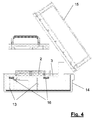
- Figure 4 is a vertical sectional view through the housing and test platform as indicated with lines 4-4 in Figure 3.
- Figure 5 is an isometric view along the same section shown in Figure 4.
- Figure 6 is a bottom isometric view of the test fixture showing the bottom of the test platform with electrical contacts and platform magnetic members housed beneath the platform and showing the device retention cover with a receiving socket for receiving the electronic device therein.
- Figure 7 is a detailed sectional view along lines 7-7 of Figure 2.
- test fixture for testing an electronic device, including: a test platform including electrically conductive contacts protruding from a device receiving surface in the test platform; a positioning guide disposed on the device receiving surface; a device retention cover; where the test platform includes a platform magnetic member and the retention cover includes a cover magnetic member, the platform magnetic member and the cover magnetic member being mutually magnetically attractive.
- a method of producing an electronic device including: preparing the test fixture, for testing the electronic device; placing the electronic device using the at least one device positioning guide disposed on the device receiving surface; and placing the device retention cover upon the electronic device to apply a force to the electronic device.
- test fixture 1 is provided for testing an electronic device 2 such as the illustrated circuit board for a wireless communication device.
- the test fixture 1 includes a test platform 3 including electrically conducting contacts 4 (best seen in Figure 1) which protrude from a device receiving surface 5 of the test platform 3.
- the test platform 3 includes device positioning guides 6 disposed on the device receiving surface 5.
- the device positioning guides 6 comprise cylindrical pins.
- various other device positioning guides 6 can be provided such as planar members, shape conforming surfaces or rectangular protrusions for example.
- test platform 3 can be easily reconfigured for various types of electronic devices 2 by removing the cylindrical pins 6 and relocating guides to different positions to accommodate different electronic devices 2.
- the device retention cover 7 in the embodiment shown is a simple rectangular machined plate having a manual grip 8. As best seen in Figure 6, the device retention cover 7 preferably includes a device receiving socket 9 that engages the device 2 and exerts a downward pressure to maintain adequate contact with the electrically conducting contacts 4.
- the device retention cover 7 is manually positioned using cylindrical recesses 10 positioned to match the cylindrical pins 6. Further, to guide the cover 7, the test platform 3 includes three peripheral walls 11 disposed on the device receiving surface 5 each aligned with an outside edge of the retention cover 7 when the retention cover 7 is a covered position over the electronic device 2. To improve manual guiding of the cover 7, the peripheral wall 11 includes an inwardly chamfered cover guiding edge 12.
- the text platform 3 includes adjustable height removable support legs 13 and is housed within a container housing 14 with a hinged lid 15 for access.
- the support leg 13 provides adaptability to change the test fixture 1 for varying sizes of electronic devices 2
- the containment housing 14 being a simple rectangular housing with hinged lid 15 can be adapted for various sizes and shapes of electronic devices 2 for testing.
- the containment housing 14 comprises a radio frequency blocking enclosure.
- other protective environments can be provided in a like manner such as noise suppression housing, a dust proof housing or a temperature control housing.
- the test platform 3 includes a platform magnetic member 16 as illustrated in each of the four corners.
- the retention cover 7 likewise includes four cover magnetic members 17 are removably housed within a recess socket 18. It will be understood that in order to exert a clamping pressure on the electronic device 2, that the platform magnetic members 16 and the cover magnetic members 17 are mutually magnetically attractive. The degree of compressive force applied by the retention cover 7 can be easily modified by selecting appropriate permanent magnets for the platform magnetic member 16 and retention cover member 17.
- the platform magnetic members 16 and retention cover magnetic members 17 are preferably mutually aligned on an axis normal to the test platform 3 as illustrated in the accompanying drawings. Alignment avoids any twisting of the cover 7 relative to the test platform 3 during installation and withdrawal.
- the components of the test fixture 1 are preferably modular in design, easily removed and replaced in various positions.
- the modular design results in easy modification, flexibility and relative low cost.
- the test fixture 1 is low cost and small size having only one moving part, the cover 7, that is manually positioned. Wear and tear of the fixture 1, maintenance and calibration are substantially reduced if not completely eliminated.
- the manual operation will alert the person performing the test to any misalignment or malfunction. As a result, safe operation is ensured, the device requires less space than mechanically operating clamping devices, and will be longer lasting requiring little maintenance while remaining simple to modify for various manufacturing applications.
Landscapes
- Engineering & Computer Science (AREA)
- Computer Hardware Design (AREA)
- Microelectronics & Electronic Packaging (AREA)
- General Engineering & Computer Science (AREA)
- Physics & Mathematics (AREA)
- General Physics & Mathematics (AREA)
- Testing Of Individual Semiconductor Devices (AREA)
- Testing Electric Properties And Detecting Electric Faults (AREA)
- Sampling And Sample Adjustment (AREA)
- Investigating Strength Of Materials By Application Of Mechanical Stress (AREA)
Abstract
Description
- An electronic component testing fixture positions and then clamps a component between a test bed platform and a manually removable clamping plate using magnetic attractive force.
- The testing of electronic components or devices during manufacturing involves use of a test fixture to accurately position the device under test so that electrical contacts are properly engaged to perform the test. Inaccurate placement or lack of appropriate electrical contact could result in a false rejection of the device under test and significant waste.
- For example, power contacts and control system contacts on circuit board devices are engaged with matching contacts on a test fixture by manually or mechanically placing the circuit board device on the test fixture. Guide pins or other physical barriers are located on the test bed to accurately guide and locate the device to be tested into the correct testing position.
- In the in use application of a circuit board device, the electrical contacts may be soldered, or engaged with tight fitting connectors, and the circuit boards are usually snap-locked, fastened or clamped securely in a housing to avoid malfunctions or short circuits in use.
- However, in a test fixture, such secure means of making electrical contacts are inefficient and would interfere with the speed of testing required during manufacture. Test fixtures therefore include temporary means of making electrical contact which minimize the risk damage to the device under test and which aim to involve minimal time in positioning and withdrawing the devices under test to increase the speed of testing.
- Since many electronic devices are very light weight and flexible, merely placing the devices in a test fixture is insufficient to ensure that proper electrical contact is made. Commonly the device is physically clamped to exert pressure on the matching electric contacts and ensure that a reliable connection is made for conducting the testing procedure.
- Pneumatic, hydraulic or mechanical clamping systems, including robotic systems are commonly used for this clamping function. However, all such systems require physical space in the manufacturing facility, require maintenance due to inevitable wear and tear of moving parts, and require periodic adjustments to maintain accuracy, consume power, impose operating and capital costs, and often create significant noise or safety hazards. In many cases, the test fixture and associated clamping system must be housed within a protective housing such as a radio frequency housing, a noise suppression housing, a dust proof housing, a temperature controlled housing or other protected environments. The use of mechanical, pneumatic or hydraulic clamping systems significantly increases the necessary space volume of any protective enclosure consuming manufacturing space and imposing various costs on the manufacturing process.
- In order that the subject matter may be readily understood, one embodiment of the subject matter is illustrated by way of example in the accompanying drawings.
- Figure 1 is a top isometric view of one embodiment showing a test fixture with test platform with cylindrical pins as device positioning guides and at an elevated position a retention cover with manual grip handle having matching cylindrical recesses and having a cylindrical recess socket in each corner to house permanent corner.
- Figure 2 is a like top isometric view showing an electronic device positioned on the electrically conductive contacts protruding from the test platform and aligned by the cylindrical pins serving as device positioning guides.
- Figure 3 is a front isometric view showing the electronic device for testing position within the test platform and showing containment housing with hinged lid surrounding the entire test platform.
- Figure 4 is a vertical sectional view through the housing and test platform as indicated with lines 4-4 in Figure 3.
- Figure 5 is an isometric view along the same section shown in Figure 4.
- Figure 6 is a bottom isometric view of the test fixture showing the bottom of the test platform with electrical contacts and platform magnetic members housed beneath the platform and showing the device retention cover with a receiving socket for receiving the electronic device therein.
- Figure 7 is a detailed sectional view along lines 7-7 of Figure 2.
- Further details of the test fixture and its advantages will be apparent from the detailed description included below.
- There is provided a test fixture, for testing an electronic device, including: a test platform including electrically conductive contacts protruding from a device receiving surface in the test platform; a positioning guide disposed on the device receiving surface; a device retention cover; where the test platform includes a platform magnetic member and the retention cover includes a cover magnetic member, the platform magnetic member and the cover magnetic member being mutually magnetically attractive.
- Further, there is provided a method of producing an electronic device including: preparing the test fixture, for testing the electronic device; placing the electronic device using the at least one device positioning guide disposed on the device receiving surface; and placing the device retention cover upon the electronic device to apply a force to the electronic device.
- With reference to Figures 1 and 2, the
test fixture 1 is provided for testing anelectronic device 2 such as the illustrated circuit board for a wireless communication device. - The
test fixture 1 includes atest platform 3 including electrically conducting contacts 4 (best seen in Figure 1) which protrude from adevice receiving surface 5 of thetest platform 3. - As best seen in Figures 2 and 3, the
test platform 3 includesdevice positioning guides 6 disposed on thedevice receiving surface 5. In the embodiment illustrated, thedevice positioning guides 6 comprise cylindrical pins. However, it will understood that depending on the configuration of theelectronic device 2, various otherdevice positioning guides 6 can be provided such as planar members, shape conforming surfaces or rectangular protrusions for example. - It will also be understood that the
test platform 3 can be easily reconfigured for various types ofelectronic devices 2 by removing thecylindrical pins 6 and relocating guides to different positions to accommodate differentelectronic devices 2. - The
device retention cover 7 in the embodiment shown is a simple rectangular machined plate having amanual grip 8. As best seen in Figure 6, thedevice retention cover 7 preferably includes a device receiving socket 9 that engages thedevice 2 and exerts a downward pressure to maintain adequate contact with the electrically conductingcontacts 4. - The
device retention cover 7 is manually positioned usingcylindrical recesses 10 positioned to match thecylindrical pins 6. Further, to guide thecover 7, thetest platform 3 includes threeperipheral walls 11 disposed on thedevice receiving surface 5 each aligned with an outside edge of theretention cover 7 when theretention cover 7 is a covered position over theelectronic device 2. To improve manual guiding of thecover 7, theperipheral wall 11 includes an inwardly chamferedcover guiding edge 12. - As shown in Figures 4 and 6, preferably the
text platform 3 includes adjustable heightremovable support legs 13 and is housed within acontainer housing 14 with ahinged lid 15 for access. As illustrated, thesupport leg 13 provides adaptability to change thetest fixture 1 for varying sizes ofelectronic devices 2 and thecontainment housing 14 being a simple rectangular housing with hingedlid 15 can be adapted for various sizes and shapes ofelectronic devices 2 for testing. In one embodiment for example, thecontainment housing 14 comprises a radio frequency blocking enclosure. However, other protective environments can be provided in a like manner such as noise suppression housing, a dust proof housing or a temperature control housing. - Turning to Figures 1, 4 and 6, it can be seen that the
test platform 3 includes a platformmagnetic member 16 as illustrated in each of the four corners. Theretention cover 7 likewise includes four cover magnetic members 17 are removably housed within a recess socket 18. It will be understood that in order to exert a clamping pressure on theelectronic device 2, that the platformmagnetic members 16 and the cover magnetic members 17 are mutually magnetically attractive. The degree of compressive force applied by theretention cover 7 can be easily modified by selecting appropriate permanent magnets for the platformmagnetic member 16 and retention cover member 17. - The platform
magnetic members 16 and retention cover magnetic members 17 are preferably mutually aligned on an axis normal to thetest platform 3 as illustrated in the accompanying drawings. Alignment avoids any twisting of thecover 7 relative to thetest platform 3 during installation and withdrawal. - As illustrated, the components of the
test fixture 1 are preferably modular in design, easily removed and replaced in various positions. The modular design results in easy modification, flexibility and relative low cost. Compared to mechanical clamping systems, pneumatic or hydraulically actuated clamping devices, thetest fixture 1 is low cost and small size having only one moving part, thecover 7, that is manually positioned. Wear and tear of thefixture 1, maintenance and calibration are substantially reduced if not completely eliminated. The manual operation will alert the person performing the test to any misalignment or malfunction. As a result, safe operation is ensured, the device requires less space than mechanically operating clamping devices, and will be longer lasting requiring little maintenance while remaining simple to modify for various manufacturing applications.
Claims (19)
- A test fixture (1), for testing an electronic device (2), comprising:a test platform (3) comprising electrically conductive contacts (4) on a device receiving surface (5) thereof;at least one device positioning guide (6) disposed on said device receiving surface (5);a device retention cover (7)wherein the test platform (3) comprises a platform magnetic member (16) and the retention cover (7) comprises a cover magnetic member (17), the platform magnetic member (16) and the cover magnetic member (17) being mutually magnetically attractive.
- A test fixture (1) according to claim 1 wherein at least one of the platform magnetic member (16) and the cover magnetic member (17) comprise a permanent magnet.
- A test fixture (1) according to claim 1 or claim 2 wherein the platform magnetic member (16) and the cover magnetic member (17) are mutually aligned on an axis normal to the test platform (3).
- A test fixture (1) according to any one of claims 1 to 3 wherein the cover magnetic member (17) is removably housed within recessed socket (18).
- A test fixture (1) according to any one of claims 1 to 4 wherein the at least one device positioning guide (6) comprises a cylindrical pin (6).
- A test fixture (1) according to claim 5 wherein the retention cover (7) comprises at least one recess (10) matching said cylindrical pin (6).
- A test fixture (1) according to any one of claims 1 to 6 wherein the test platform (3) comprises at least one cover alignment guide (11) disposed on said device receiving surface (5).
- A test fixture (1) according to claim 7 wherein the at least one cover alignment guide (11) comprises a peripheral wall (11) aligned with an outside edge of the retention cover (7) in a covered position.
- A test fixture (1) according to claim 8 wherein the peripheral wall (11) comprises an inwardly chamfered cover guiding edge (12).
- A test fixture (1) according to any one of claims 1 to 9 wherein the retention cover (7) has a test platform facing surface with a device receiving socket (9).
- A test fixture (1) according to claim 10 wherein the retention cover (7) has a manual grip (8).
- A test fixture (1) according to any one of claims 1 to 11 wherein the test platform (3) comprises support legs (13).
- A test fixture (1) according to any one of claims 1 to 12 wherein the test platform (3) comprises a containment housing (14).
- A test fixture (1) according to claim 13 wherein the containment housing (14) comprises a radio frequency blocking enclosure.
- A test fixture (1) according to claim 13 or claim 14 wherein the containment housing (14) has a hinged lid (15).
- A method of producing an electronic device, comprising:preparing a test fixture (1) according to any one of claims 1 to 15, for testing the electronic device (2);placing the electronic device (2) using the at least one device positioning guide (6) disposed on said device receiving surface (5); andplacing the device retention cover (7) upon the electronic device (2) to apply a force to the electronic device (2).
- A method according to claim 16 wherein the step of placing the electronic device (2) on said device receiving surface (5) is manually performed.
- A method according to claim 16 or claim 17 wherein the step of placing the device retention cover (7) upon the electronic device (2) to apply a force to the electronic device (2) is manually performed.
- A method according to any one of claims 16 to 18 wherein the method comprises the further step of closing the lid (15) after the step of placing the device retention cover (7) upon the electronic device (2).
Priority Applications (4)
| Application Number | Priority Date | Filing Date | Title |
|---|---|---|---|
| EP05107610A EP1754976B1 (en) | 2005-08-18 | 2005-08-18 | Test Fixture With Clamping Top Plate Using Magnetic Force |
| AT05107610T ATE483167T1 (en) | 2005-08-18 | 2005-08-18 | TEST HOLDER WITH COVER PLATE FOR LOCKING USING MAGNETIC FORCE |
| DE602005023863T DE602005023863D1 (en) | 2005-08-18 | 2005-08-18 | Test holder with cover plate for magnetic force locking |
| CA2550176A CA2550176C (en) | 2005-08-18 | 2006-06-14 | Clamping top plate using magnetic force |
Applications Claiming Priority (1)
| Application Number | Priority Date | Filing Date | Title |
|---|---|---|---|
| EP05107610A EP1754976B1 (en) | 2005-08-18 | 2005-08-18 | Test Fixture With Clamping Top Plate Using Magnetic Force |
Publications (2)
| Publication Number | Publication Date |
|---|---|
| EP1754976A1 true EP1754976A1 (en) | 2007-02-21 |
| EP1754976B1 EP1754976B1 (en) | 2010-09-29 |
Family
ID=35658895
Family Applications (1)
| Application Number | Title | Priority Date | Filing Date |
|---|---|---|---|
| EP05107610A Expired - Lifetime EP1754976B1 (en) | 2005-08-18 | 2005-08-18 | Test Fixture With Clamping Top Plate Using Magnetic Force |
Country Status (4)
| Country | Link |
|---|---|
| EP (1) | EP1754976B1 (en) |
| AT (1) | ATE483167T1 (en) |
| CA (1) | CA2550176C (en) |
| DE (1) | DE602005023863D1 (en) |
Cited By (10)
| Publication number | Priority date | Publication date | Assignee | Title |
|---|---|---|---|---|
| CN103165314A (en) * | 2011-12-11 | 2013-06-19 | 湖北港源电气有限公司 | Light touch switch |
| DE102012209353A1 (en) * | 2012-06-04 | 2013-12-05 | Continental Automotive Gmbh | Test device for testing a printed circuit board |
| ITRM20130545A1 (en) * | 2013-10-04 | 2015-04-05 | Enea Agenzia Naz Per Le Nuo Ve Tecnologie | "FIXING DEVICE FOR ORGANIC, INORGANIC OR HYBRID ELECTRONIC DEVICES FOR MEASUREMENTS IN THE ENVIRONMENT WITH CONTROLLED OR VACUUM ATMOSPHERE" |
| US9410907B2 (en) | 2013-12-19 | 2016-08-09 | Clarus Vision, Inc. | Methods and apparatuses for testing capacitive touch screen films |
| CN111137807A (en) * | 2019-12-12 | 2020-05-12 | 苏州市运泰利自动化设备有限公司 | A large-scale pneumatic lifting platform with automatic locking |
| DE102011054260B4 (en) | 2011-10-06 | 2020-06-18 | Ingun Prüfmittelbau Gmbh | Device and method for testing printed circuit boards |
| CN113791246A (en) * | 2021-09-01 | 2021-12-14 | 广东凯威检测技术股份有限公司 | Radio frequency conduction test fixture |
| CN115014608A (en) * | 2022-06-06 | 2022-09-06 | 江西永旺磁力检测有限公司 | Magnetic field jacking force testing equipment and magnetic force testing method |
| CN118483457A (en) * | 2024-04-11 | 2024-08-13 | 徐州领测半导体科技有限公司 | Integrated circuit test fixture with position correction function |
| KR102893253B1 (en) * | 2024-06-19 | 2025-12-03 | (주)티에이치엔 | Jig for instant short circuit test |
Citations (5)
| Publication number | Priority date | Publication date | Assignee | Title |
|---|---|---|---|---|
| US5572144A (en) * | 1993-02-22 | 1996-11-05 | Seagate Technology | Test jig and method for probing a printed circuit board |
| US5831160A (en) * | 1997-05-22 | 1998-11-03 | Hewlett-Packard Company | Test fixture clamping system |
| US20020074993A1 (en) * | 2000-02-23 | 2002-06-20 | Boswell Bryan D. | RF isolation test device accommodating multiple nest plates for testing different devices and providing variable testing options |
| US20040226167A1 (en) * | 2003-05-14 | 2004-11-18 | Benq Corporation | Screw mounting jig |
| US20040257097A1 (en) * | 2003-06-19 | 2004-12-23 | Serge Beaucag | Vacuum-actuated test fixture for testing printed circuit boards |
-
2005
- 2005-08-18 DE DE602005023863T patent/DE602005023863D1/en not_active Expired - Lifetime
- 2005-08-18 EP EP05107610A patent/EP1754976B1/en not_active Expired - Lifetime
- 2005-08-18 AT AT05107610T patent/ATE483167T1/en not_active IP Right Cessation
-
2006
- 2006-06-14 CA CA2550176A patent/CA2550176C/en active Active
Patent Citations (5)
| Publication number | Priority date | Publication date | Assignee | Title |
|---|---|---|---|---|
| US5572144A (en) * | 1993-02-22 | 1996-11-05 | Seagate Technology | Test jig and method for probing a printed circuit board |
| US5831160A (en) * | 1997-05-22 | 1998-11-03 | Hewlett-Packard Company | Test fixture clamping system |
| US20020074993A1 (en) * | 2000-02-23 | 2002-06-20 | Boswell Bryan D. | RF isolation test device accommodating multiple nest plates for testing different devices and providing variable testing options |
| US20040226167A1 (en) * | 2003-05-14 | 2004-11-18 | Benq Corporation | Screw mounting jig |
| US20040257097A1 (en) * | 2003-06-19 | 2004-12-23 | Serge Beaucag | Vacuum-actuated test fixture for testing printed circuit boards |
Cited By (13)
| Publication number | Priority date | Publication date | Assignee | Title |
|---|---|---|---|---|
| DE102011054260B4 (en) | 2011-10-06 | 2020-06-18 | Ingun Prüfmittelbau Gmbh | Device and method for testing printed circuit boards |
| CN103165314A (en) * | 2011-12-11 | 2013-06-19 | 湖北港源电气有限公司 | Light touch switch |
| DE102012209353A1 (en) * | 2012-06-04 | 2013-12-05 | Continental Automotive Gmbh | Test device for testing a printed circuit board |
| US9632132B2 (en) | 2012-06-04 | 2017-04-25 | Continental Automotive Gmbh | Test device for testing a flat module |
| DE102012209353B4 (en) | 2012-06-04 | 2018-12-06 | Continental Automotive Gmbh | Test device for testing a printed circuit board |
| ITRM20130545A1 (en) * | 2013-10-04 | 2015-04-05 | Enea Agenzia Naz Per Le Nuo Ve Tecnologie | "FIXING DEVICE FOR ORGANIC, INORGANIC OR HYBRID ELECTRONIC DEVICES FOR MEASUREMENTS IN THE ENVIRONMENT WITH CONTROLLED OR VACUUM ATMOSPHERE" |
| US9410907B2 (en) | 2013-12-19 | 2016-08-09 | Clarus Vision, Inc. | Methods and apparatuses for testing capacitive touch screen films |
| CN111137807A (en) * | 2019-12-12 | 2020-05-12 | 苏州市运泰利自动化设备有限公司 | A large-scale pneumatic lifting platform with automatic locking |
| CN113791246A (en) * | 2021-09-01 | 2021-12-14 | 广东凯威检测技术股份有限公司 | Radio frequency conduction test fixture |
| CN113791246B (en) * | 2021-09-01 | 2023-11-28 | 凯威检测科技(广东)有限公司 | Radio frequency conduction test fixture |
| CN115014608A (en) * | 2022-06-06 | 2022-09-06 | 江西永旺磁力检测有限公司 | Magnetic field jacking force testing equipment and magnetic force testing method |
| CN118483457A (en) * | 2024-04-11 | 2024-08-13 | 徐州领测半导体科技有限公司 | Integrated circuit test fixture with position correction function |
| KR102893253B1 (en) * | 2024-06-19 | 2025-12-03 | (주)티에이치엔 | Jig for instant short circuit test |
Also Published As
| Publication number | Publication date |
|---|---|
| ATE483167T1 (en) | 2010-10-15 |
| CA2550176A1 (en) | 2007-02-18 |
| CA2550176C (en) | 2012-04-10 |
| DE602005023863D1 (en) | 2010-11-11 |
| EP1754976B1 (en) | 2010-09-29 |
Similar Documents
| Publication | Publication Date | Title |
|---|---|---|
| US7755378B2 (en) | Clamping top plate using magnetic force | |
| EP1754976A1 (en) | Test Fixture With Clamping Top Plate Using Magnetic Force | |
| EP1995602B1 (en) | Probe board, test fixture, method for making a probe board, and method for testing a printed circuit board | |
| US7470140B1 (en) | Integrated chip clamp adjustment assembly and method | |
| DE60315813D1 (en) | DEVICE FOR AN INTERFACE BETWEEN ELECTRONIC HOUSINGS AND TEST DEVICES | |
| US20140082926A1 (en) | Conformal fixture cover | |
| CN209927971U (en) | Drawer type circuit board automatic checkout device | |
| CN215986200U (en) | Drawbridge drawer type electromagnetic shielding box | |
| EP0454347A2 (en) | Vacuum-actuated test fixture for testing electronic components | |
| KR20250040529A (en) | Wafer Test System | |
| CA1269758A (en) | Electronic test fixture with cassette system | |
| KR20140114683A (en) | Jig for examining product with printed circuit with connecting guide | |
| KR102661512B1 (en) | Electrostatic chuck filter box and mounting bracket | |
| US6672914B1 (en) | Methods and apparatus for mounting a bus bar assembly | |
| US20250239428A1 (en) | Spare fuse clip | |
| US6262571B1 (en) | Adjustable electrical connector for test fixture nest | |
| US20090075514A1 (en) | Test socket | |
| US20240052870A1 (en) | Flexible Shoulder Pin Module For Installing A Panel On An Assembly | |
| US5801543A (en) | Device for testing printed circuit boards and/or flat modules | |
| CN223692478U (en) | Fully automatic circuit testing equipment | |
| US9702741B2 (en) | In store display calibration system | |
| CN217241070U (en) | Circuit board press fitting equipment | |
| KR102681161B1 (en) | Semiconductor package test socket mounting jig | |
| CN224012086U (en) | A work platform adaptable to different EPS controller housings | |
| CN211878120U (en) | Fixing device for detecting printed circuit board |
Legal Events
| Date | Code | Title | Description |
|---|---|---|---|
| PUAI | Public reference made under article 153(3) epc to a published international application that has entered the european phase |
Free format text: ORIGINAL CODE: 0009012 |
|
| 17P | Request for examination filed |
Effective date: 20050818 |
|
| AK | Designated contracting states |
Kind code of ref document: A1 Designated state(s): AT BE BG CH CY CZ DE DK EE ES FI FR GB GR HU IE IS IT LI LT LU LV MC NL PL PT RO SE SI SK TR |
|
| AX | Request for extension of the european patent |
Extension state: AL BA HR MK YU |
|
| 17Q | First examination report despatched |
Effective date: 20070209 |
|
| AKX | Designation fees paid |
Designated state(s): AT BE BG CH CY CZ DE DK EE ES FI FR GB GR HU IE IS IT LI LT LU LV MC NL PL PT RO SE SI SK TR |
|
| AXX | Extension fees paid |
Extension state: HR Payment date: 20050818 Extension state: AL Payment date: 20050818 Extension state: YU Payment date: 20050818 Extension state: MK Payment date: 20050818 Extension state: BA Payment date: 20050818 |
|
| GRAP | Despatch of communication of intention to grant a patent |
Free format text: ORIGINAL CODE: EPIDOSNIGR1 |
|
| GRAS | Grant fee paid |
Free format text: ORIGINAL CODE: EPIDOSNIGR3 |
|
| GRAA | (expected) grant |
Free format text: ORIGINAL CODE: 0009210 |
|
| AK | Designated contracting states |
Kind code of ref document: B1 Designated state(s): AT BE BG CH CY CZ DE DK EE ES FI FR GB GR HU IE IS IT LI LT LU LV MC NL PL PT RO SE SI SK TR |
|
| AX | Request for extension of the european patent |
Extension state: AL BA HR MK YU |
|
| REG | Reference to a national code |
Ref country code: GB Ref legal event code: FG4D |
|
| REG | Reference to a national code |
Ref country code: CH Ref legal event code: EP |
|
| REG | Reference to a national code |
Ref country code: IE Ref legal event code: FG4D |
|
| REF | Corresponds to: |
Ref document number: 602005023863 Country of ref document: DE Date of ref document: 20101111 Kind code of ref document: P |
|
| PG25 | Lapsed in a contracting state [announced via postgrant information from national office to epo] |
Ref country code: LT Free format text: LAPSE BECAUSE OF FAILURE TO SUBMIT A TRANSLATION OF THE DESCRIPTION OR TO PAY THE FEE WITHIN THE PRESCRIBED TIME-LIMIT Effective date: 20100929 Ref country code: FI Free format text: LAPSE BECAUSE OF FAILURE TO SUBMIT A TRANSLATION OF THE DESCRIPTION OR TO PAY THE FEE WITHIN THE PRESCRIBED TIME-LIMIT Effective date: 20100929 Ref country code: AT Free format text: LAPSE BECAUSE OF FAILURE TO SUBMIT A TRANSLATION OF THE DESCRIPTION OR TO PAY THE FEE WITHIN THE PRESCRIBED TIME-LIMIT Effective date: 20100929 |
|
| REG | Reference to a national code |
Ref country code: NL Ref legal event code: VDEP Effective date: 20100929 |
|
| LTIE | Lt: invalidation of european patent or patent extension |
Effective date: 20100929 |
|
| PG25 | Lapsed in a contracting state [announced via postgrant information from national office to epo] |
Ref country code: SI Free format text: LAPSE BECAUSE OF FAILURE TO SUBMIT A TRANSLATION OF THE DESCRIPTION OR TO PAY THE FEE WITHIN THE PRESCRIBED TIME-LIMIT Effective date: 20100929 |
|
| PG25 | Lapsed in a contracting state [announced via postgrant information from national office to epo] |
Ref country code: GR Free format text: LAPSE BECAUSE OF FAILURE TO SUBMIT A TRANSLATION OF THE DESCRIPTION OR TO PAY THE FEE WITHIN THE PRESCRIBED TIME-LIMIT Effective date: 20101230 Ref country code: SE Free format text: LAPSE BECAUSE OF FAILURE TO SUBMIT A TRANSLATION OF THE DESCRIPTION OR TO PAY THE FEE WITHIN THE PRESCRIBED TIME-LIMIT Effective date: 20100929 Ref country code: LV Free format text: LAPSE BECAUSE OF FAILURE TO SUBMIT A TRANSLATION OF THE DESCRIPTION OR TO PAY THE FEE WITHIN THE PRESCRIBED TIME-LIMIT Effective date: 20100929 |
|
| PG25 | Lapsed in a contracting state [announced via postgrant information from national office to epo] |
Ref country code: IS Free format text: LAPSE BECAUSE OF FAILURE TO SUBMIT A TRANSLATION OF THE DESCRIPTION OR TO PAY THE FEE WITHIN THE PRESCRIBED TIME-LIMIT Effective date: 20110129 Ref country code: PT Free format text: LAPSE BECAUSE OF FAILURE TO SUBMIT A TRANSLATION OF THE DESCRIPTION OR TO PAY THE FEE WITHIN THE PRESCRIBED TIME-LIMIT Effective date: 20110131 Ref country code: NL Free format text: LAPSE BECAUSE OF FAILURE TO SUBMIT A TRANSLATION OF THE DESCRIPTION OR TO PAY THE FEE WITHIN THE PRESCRIBED TIME-LIMIT Effective date: 20100929 Ref country code: EE Free format text: LAPSE BECAUSE OF FAILURE TO SUBMIT A TRANSLATION OF THE DESCRIPTION OR TO PAY THE FEE WITHIN THE PRESCRIBED TIME-LIMIT Effective date: 20100929 Ref country code: IT Free format text: LAPSE BECAUSE OF FAILURE TO SUBMIT A TRANSLATION OF THE DESCRIPTION OR TO PAY THE FEE WITHIN THE PRESCRIBED TIME-LIMIT Effective date: 20100929 Ref country code: CZ Free format text: LAPSE BECAUSE OF FAILURE TO SUBMIT A TRANSLATION OF THE DESCRIPTION OR TO PAY THE FEE WITHIN THE PRESCRIBED TIME-LIMIT Effective date: 20100929 Ref country code: SK Free format text: LAPSE BECAUSE OF FAILURE TO SUBMIT A TRANSLATION OF THE DESCRIPTION OR TO PAY THE FEE WITHIN THE PRESCRIBED TIME-LIMIT Effective date: 20100929 Ref country code: RO Free format text: LAPSE BECAUSE OF FAILURE TO SUBMIT A TRANSLATION OF THE DESCRIPTION OR TO PAY THE FEE WITHIN THE PRESCRIBED TIME-LIMIT Effective date: 20100929 |
|
| PG25 | Lapsed in a contracting state [announced via postgrant information from national office to epo] |
Ref country code: BE Free format text: LAPSE BECAUSE OF FAILURE TO SUBMIT A TRANSLATION OF THE DESCRIPTION OR TO PAY THE FEE WITHIN THE PRESCRIBED TIME-LIMIT Effective date: 20100929 |
|
| PG25 | Lapsed in a contracting state [announced via postgrant information from national office to epo] |
Ref country code: ES Free format text: LAPSE BECAUSE OF FAILURE TO SUBMIT A TRANSLATION OF THE DESCRIPTION OR TO PAY THE FEE WITHIN THE PRESCRIBED TIME-LIMIT Effective date: 20110109 |
|
| PLBE | No opposition filed within time limit |
Free format text: ORIGINAL CODE: 0009261 |
|
| STAA | Information on the status of an ep patent application or granted ep patent |
Free format text: STATUS: NO OPPOSITION FILED WITHIN TIME LIMIT |
|
| PG25 | Lapsed in a contracting state [announced via postgrant information from national office to epo] |
Ref country code: DK Free format text: LAPSE BECAUSE OF FAILURE TO SUBMIT A TRANSLATION OF THE DESCRIPTION OR TO PAY THE FEE WITHIN THE PRESCRIBED TIME-LIMIT Effective date: 20100929 Ref country code: PL Free format text: LAPSE BECAUSE OF FAILURE TO SUBMIT A TRANSLATION OF THE DESCRIPTION OR TO PAY THE FEE WITHIN THE PRESCRIBED TIME-LIMIT Effective date: 20100929 |
|
| REG | Reference to a national code |
Ref country code: DE Ref legal event code: R097 Ref document number: 602005023863 Country of ref document: DE Effective date: 20110630 |
|
| PG25 | Lapsed in a contracting state [announced via postgrant information from national office to epo] |
Ref country code: MC Free format text: LAPSE BECAUSE OF NON-PAYMENT OF DUE FEES Effective date: 20110831 |
|
| REG | Reference to a national code |
Ref country code: CH Ref legal event code: PL |
|
| PG25 | Lapsed in a contracting state [announced via postgrant information from national office to epo] |
Ref country code: CH Free format text: LAPSE BECAUSE OF NON-PAYMENT OF DUE FEES Effective date: 20110831 Ref country code: LI Free format text: LAPSE BECAUSE OF NON-PAYMENT OF DUE FEES Effective date: 20110831 |
|
| REG | Reference to a national code |
Ref country code: IE Ref legal event code: MM4A |
|
| PG25 | Lapsed in a contracting state [announced via postgrant information from national office to epo] |
Ref country code: IE Free format text: LAPSE BECAUSE OF NON-PAYMENT OF DUE FEES Effective date: 20110818 |
|
| PG25 | Lapsed in a contracting state [announced via postgrant information from national office to epo] |
Ref country code: LU Free format text: LAPSE BECAUSE OF NON-PAYMENT OF DUE FEES Effective date: 20110818 Ref country code: CY Free format text: LAPSE BECAUSE OF EXPIRATION OF PROTECTION Effective date: 20100929 |
|
| PG25 | Lapsed in a contracting state [announced via postgrant information from national office to epo] |
Ref country code: BG Free format text: LAPSE BECAUSE OF FAILURE TO SUBMIT A TRANSLATION OF THE DESCRIPTION OR TO PAY THE FEE WITHIN THE PRESCRIBED TIME-LIMIT Effective date: 20101229 Ref country code: TR Free format text: LAPSE BECAUSE OF FAILURE TO SUBMIT A TRANSLATION OF THE DESCRIPTION OR TO PAY THE FEE WITHIN THE PRESCRIBED TIME-LIMIT Effective date: 20100929 |
|
| PG25 | Lapsed in a contracting state [announced via postgrant information from national office to epo] |
Ref country code: HU Free format text: LAPSE BECAUSE OF FAILURE TO SUBMIT A TRANSLATION OF THE DESCRIPTION OR TO PAY THE FEE WITHIN THE PRESCRIBED TIME-LIMIT Effective date: 20100929 |
|
| REG | Reference to a national code |
Ref country code: DE Ref legal event code: R082 Ref document number: 602005023863 Country of ref document: DE Representative=s name: MERH-IP MATIAS ERNY REICHL HOFFMANN, DE |
|
| REG | Reference to a national code |
Ref country code: DE Ref legal event code: R082 Ref document number: 602005023863 Country of ref document: DE Representative=s name: MERH-IP MATIAS ERNY REICHL HOFFMANN, DE Effective date: 20140925 Ref country code: DE Ref legal event code: R081 Ref document number: 602005023863 Country of ref document: DE Owner name: BLACKBERRY LIMITED, WATERLOO, CA Free format text: FORMER OWNER: RESEARCH IN MOTION LTD., WATERLOO, ONTARIO, CA Effective date: 20140925 Ref country code: DE Ref legal event code: R082 Ref document number: 602005023863 Country of ref document: DE Representative=s name: MERH-IP MATIAS ERNY REICHL HOFFMANN PATENTANWA, DE Effective date: 20140925 |
|
| REG | Reference to a national code |
Ref country code: FR Ref legal event code: PLFP Year of fee payment: 12 |
|
| REG | Reference to a national code |
Ref country code: FR Ref legal event code: PLFP Year of fee payment: 13 |
|
| REG | Reference to a national code |
Ref country code: FR Ref legal event code: PLFP Year of fee payment: 14 |
|
| REG | Reference to a national code |
Ref country code: DE Ref legal event code: R082 Ref document number: 602005023863 Country of ref document: DE Ref country code: DE Ref legal event code: R081 Ref document number: 602005023863 Country of ref document: DE Owner name: MALIKIE INNOVATIONS LTD., IE Free format text: FORMER OWNER: BLACKBERRY LIMITED, WATERLOO, ONTARIO, CA |
|
| PGFP | Annual fee paid to national office [announced via postgrant information from national office to epo] |
Ref country code: DE Payment date: 20240828 Year of fee payment: 20 |
|
| PGFP | Annual fee paid to national office [announced via postgrant information from national office to epo] |
Ref country code: GB Payment date: 20240827 Year of fee payment: 20 |
|
| PGFP | Annual fee paid to national office [announced via postgrant information from national office to epo] |
Ref country code: FR Payment date: 20240826 Year of fee payment: 20 |
|
| REG | Reference to a national code |
Ref country code: DE Ref legal event code: R071 Ref document number: 602005023863 Country of ref document: DE |
|
| REG | Reference to a national code |
Ref country code: GB Ref legal event code: PE20 Expiry date: 20250817 |