EP1754110B1 - Projection objective for a microlithographic projection exposure apparatus - Google Patents
Projection objective for a microlithographic projection exposure apparatus Download PDFInfo
- Publication number
- EP1754110B1 EP1754110B1 EP05751684A EP05751684A EP1754110B1 EP 1754110 B1 EP1754110 B1 EP 1754110B1 EP 05751684 A EP05751684 A EP 05751684A EP 05751684 A EP05751684 A EP 05751684A EP 1754110 B1 EP1754110 B1 EP 1754110B1
- Authority
- EP
- European Patent Office
- Prior art keywords
- projection objective
- projection
- section
- wavefront
- optically active
- Prior art date
- Legal status (The legal status is an assumption and is not a legal conclusion. Google has not performed a legal analysis and makes no representation as to the accuracy of the status listed.)
- Ceased
Links
Images

Classifications
-
- G—PHYSICS
- G02—OPTICS
- G02B—OPTICAL ELEMENTS, SYSTEMS OR APPARATUS
- G02B13/00—Optical objectives specially designed for the purposes specified below
- G02B13/24—Optical objectives specially designed for the purposes specified below for reproducing or copying at short object distances
-
- G—PHYSICS
- G02—OPTICS
- G02B—OPTICAL ELEMENTS, SYSTEMS OR APPARATUS
- G02B13/00—Optical objectives specially designed for the purposes specified below
- G02B13/18—Optical objectives specially designed for the purposes specified below with lenses having one or more non-spherical faces, e.g. for reducing geometrical aberration
-
- G—PHYSICS
- G02—OPTICS
- G02B—OPTICAL ELEMENTS, SYSTEMS OR APPARATUS
- G02B27/00—Optical systems or apparatus not provided for by any of the groups G02B1/00 - G02B26/00, G02B30/00
- G02B27/0025—Optical systems or apparatus not provided for by any of the groups G02B1/00 - G02B26/00, G02B30/00 for optical correction, e.g. distorsion, aberration
-
- G—PHYSICS
- G03—PHOTOGRAPHY; CINEMATOGRAPHY; ANALOGOUS TECHNIQUES USING WAVES OTHER THAN OPTICAL WAVES; ELECTROGRAPHY; HOLOGRAPHY
- G03F—PHOTOMECHANICAL PRODUCTION OF TEXTURED OR PATTERNED SURFACES, e.g. FOR PRINTING, FOR PROCESSING OF SEMICONDUCTOR DEVICES; MATERIALS THEREFOR; ORIGINALS THEREFOR; APPARATUS SPECIALLY ADAPTED THEREFOR
- G03F7/00—Photomechanical, e.g. photolithographic, production of textured or patterned surfaces, e.g. printing surfaces; Materials therefor, e.g. comprising photoresists; Apparatus specially adapted therefor
- G03F7/20—Exposure; Apparatus therefor
- G03F7/2002—Exposure; Apparatus therefor with visible light or UV light, through an original having an opaque pattern on a transparent support, e.g. film printing, projection printing; by reflection of visible or UV light from an original such as a printed image
- G03F7/2008—Exposure; Apparatus therefor with visible light or UV light, through an original having an opaque pattern on a transparent support, e.g. film printing, projection printing; by reflection of visible or UV light from an original such as a printed image characterised by the reflectors, diffusers, light or heat filtering means or anti-reflective means used
-
- G—PHYSICS
- G03—PHOTOGRAPHY; CINEMATOGRAPHY; ANALOGOUS TECHNIQUES USING WAVES OTHER THAN OPTICAL WAVES; ELECTROGRAPHY; HOLOGRAPHY
- G03F—PHOTOMECHANICAL PRODUCTION OF TEXTURED OR PATTERNED SURFACES, e.g. FOR PRINTING, FOR PROCESSING OF SEMICONDUCTOR DEVICES; MATERIALS THEREFOR; ORIGINALS THEREFOR; APPARATUS SPECIALLY ADAPTED THEREFOR
- G03F7/00—Photomechanical, e.g. photolithographic, production of textured or patterned surfaces, e.g. printing surfaces; Materials therefor, e.g. comprising photoresists; Apparatus specially adapted therefor
- G03F7/70—Microphotolithographic exposure; Apparatus therefor
- G03F7/70058—Mask illumination systems
- G03F7/7015—Details of optical elements
-
- G—PHYSICS
- G03—PHOTOGRAPHY; CINEMATOGRAPHY; ANALOGOUS TECHNIQUES USING WAVES OTHER THAN OPTICAL WAVES; ELECTROGRAPHY; HOLOGRAPHY
- G03F—PHOTOMECHANICAL PRODUCTION OF TEXTURED OR PATTERNED SURFACES, e.g. FOR PRINTING, FOR PROCESSING OF SEMICONDUCTOR DEVICES; MATERIALS THEREFOR; ORIGINALS THEREFOR; APPARATUS SPECIALLY ADAPTED THEREFOR
- G03F7/00—Photomechanical, e.g. photolithographic, production of textured or patterned surfaces, e.g. printing surfaces; Materials therefor, e.g. comprising photoresists; Apparatus specially adapted therefor
- G03F7/70—Microphotolithographic exposure; Apparatus therefor
- G03F7/70058—Mask illumination systems
- G03F7/70191—Optical correction elements, filters or phase plates for controlling intensity, wavelength, polarisation, phase or the like
-
- G—PHYSICS
- G03—PHOTOGRAPHY; CINEMATOGRAPHY; ANALOGOUS TECHNIQUES USING WAVES OTHER THAN OPTICAL WAVES; ELECTROGRAPHY; HOLOGRAPHY
- G03F—PHOTOMECHANICAL PRODUCTION OF TEXTURED OR PATTERNED SURFACES, e.g. FOR PRINTING, FOR PROCESSING OF SEMICONDUCTOR DEVICES; MATERIALS THEREFOR; ORIGINALS THEREFOR; APPARATUS SPECIALLY ADAPTED THEREFOR
- G03F7/00—Photomechanical, e.g. photolithographic, production of textured or patterned surfaces, e.g. printing surfaces; Materials therefor, e.g. comprising photoresists; Apparatus specially adapted therefor
- G03F7/70—Microphotolithographic exposure; Apparatus therefor
- G03F7/70216—Mask projection systems
- G03F7/70225—Optical aspects of catadioptric systems, i.e. comprising reflective and refractive elements
-
- G—PHYSICS
- G03—PHOTOGRAPHY; CINEMATOGRAPHY; ANALOGOUS TECHNIQUES USING WAVES OTHER THAN OPTICAL WAVES; ELECTROGRAPHY; HOLOGRAPHY
- G03F—PHOTOMECHANICAL PRODUCTION OF TEXTURED OR PATTERNED SURFACES, e.g. FOR PRINTING, FOR PROCESSING OF SEMICONDUCTOR DEVICES; MATERIALS THEREFOR; ORIGINALS THEREFOR; APPARATUS SPECIALLY ADAPTED THEREFOR
- G03F7/00—Photomechanical, e.g. photolithographic, production of textured or patterned surfaces, e.g. printing surfaces; Materials therefor, e.g. comprising photoresists; Apparatus specially adapted therefor
- G03F7/70—Microphotolithographic exposure; Apparatus therefor
- G03F7/70216—Mask projection systems
- G03F7/70308—Optical correction elements, filters or phase plates for manipulating imaging light, e.g. intensity, wavelength, polarisation, phase or image shift
-
- G—PHYSICS
- G03—PHOTOGRAPHY; CINEMATOGRAPHY; ANALOGOUS TECHNIQUES USING WAVES OTHER THAN OPTICAL WAVES; ELECTROGRAPHY; HOLOGRAPHY
- G03F—PHOTOMECHANICAL PRODUCTION OF TEXTURED OR PATTERNED SURFACES, e.g. FOR PRINTING, FOR PROCESSING OF SEMICONDUCTOR DEVICES; MATERIALS THEREFOR; ORIGINALS THEREFOR; APPARATUS SPECIALLY ADAPTED THEREFOR
- G03F7/00—Photomechanical, e.g. photolithographic, production of textured or patterned surfaces, e.g. printing surfaces; Materials therefor, e.g. comprising photoresists; Apparatus specially adapted therefor
- G03F7/70—Microphotolithographic exposure; Apparatus therefor
- G03F7/70483—Information management; Active and passive control; Testing; Wafer monitoring, e.g. pattern monitoring
- G03F7/70591—Testing optical components
-
- G—PHYSICS
- G03—PHOTOGRAPHY; CINEMATOGRAPHY; ANALOGOUS TECHNIQUES USING WAVES OTHER THAN OPTICAL WAVES; ELECTROGRAPHY; HOLOGRAPHY
- G03F—PHOTOMECHANICAL PRODUCTION OF TEXTURED OR PATTERNED SURFACES, e.g. FOR PRINTING, FOR PROCESSING OF SEMICONDUCTOR DEVICES; MATERIALS THEREFOR; ORIGINALS THEREFOR; APPARATUS SPECIALLY ADAPTED THEREFOR
- G03F7/00—Photomechanical, e.g. photolithographic, production of textured or patterned surfaces, e.g. printing surfaces; Materials therefor, e.g. comprising photoresists; Apparatus specially adapted therefor
- G03F7/70—Microphotolithographic exposure; Apparatus therefor
- G03F7/70483—Information management; Active and passive control; Testing; Wafer monitoring, e.g. pattern monitoring
- G03F7/70591—Testing optical components
- G03F7/706—Aberration measurement
-
- G—PHYSICS
- G03—PHOTOGRAPHY; CINEMATOGRAPHY; ANALOGOUS TECHNIQUES USING WAVES OTHER THAN OPTICAL WAVES; ELECTROGRAPHY; HOLOGRAPHY
- G03F—PHOTOMECHANICAL PRODUCTION OF TEXTURED OR PATTERNED SURFACES, e.g. FOR PRINTING, FOR PROCESSING OF SEMICONDUCTOR DEVICES; MATERIALS THEREFOR; ORIGINALS THEREFOR; APPARATUS SPECIALLY ADAPTED THEREFOR
- G03F7/00—Photomechanical, e.g. photolithographic, production of textured or patterned surfaces, e.g. printing surfaces; Materials therefor, e.g. comprising photoresists; Apparatus specially adapted therefor
- G03F7/70—Microphotolithographic exposure; Apparatus therefor
- G03F7/708—Construction of apparatus, e.g. environment aspects, hygiene aspects or materials
- G03F7/70975—Assembly, maintenance, transport or storage of apparatus
-
- H—ELECTRICITY
- H10—SEMICONDUCTOR DEVICES; ELECTRIC SOLID-STATE DEVICES NOT OTHERWISE PROVIDED FOR
- H10P—GENERIC PROCESSES OR APPARATUS FOR THE MANUFACTURE OR TREATMENT OF DEVICES COVERED BY CLASS H10
- H10P76/00—Manufacture or treatment of masks on semiconductor bodies, e.g. by lithography or photolithography
- H10P76/20—Manufacture or treatment of masks on semiconductor bodies, e.g. by lithography or photolithography of masks comprising organic materials
- H10P76/204—Manufacture or treatment of masks on semiconductor bodies, e.g. by lithography or photolithography of masks comprising organic materials of organic photoresist masks
- H10P76/2041—Photolithographic processes
-
- G—PHYSICS
- G03—PHOTOGRAPHY; CINEMATOGRAPHY; ANALOGOUS TECHNIQUES USING WAVES OTHER THAN OPTICAL WAVES; ELECTROGRAPHY; HOLOGRAPHY
- G03F—PHOTOMECHANICAL PRODUCTION OF TEXTURED OR PATTERNED SURFACES, e.g. FOR PRINTING, FOR PROCESSING OF SEMICONDUCTOR DEVICES; MATERIALS THEREFOR; ORIGINALS THEREFOR; APPARATUS SPECIALLY ADAPTED THEREFOR
- G03F7/00—Photomechanical, e.g. photolithographic, production of textured or patterned surfaces, e.g. printing surfaces; Materials therefor, e.g. comprising photoresists; Apparatus specially adapted therefor
- G03F7/70—Microphotolithographic exposure; Apparatus therefor
- G03F7/70216—Mask projection systems
- G03F7/70241—Optical aspects of refractive lens systems, i.e. comprising only refractive elements
Definitions
- the invention relates to a projection objective for microlithographic projection exposure apparatus, such as those used for the production of microstructured components.
- Microlithographic projection exposure apparatus such as those used for the production of large-scale integrated electrical circuits, have an illumination device which is used to generate a projection light beam.
- the projection light beam is aimed at a reticle which contains structures to be imaged by the projection exposure system, and which is arranged in an object plane of a projection objective.
- the projection objective forms a reduced image of the structures of the reticle on a photosensitive surface, which is located an image plane of the projection objective and may for example be applied on a wafer.
- Imaging errors can therefore be tolerated only to a very small extent.
- imaging errors which occur are assigned to the following categories.
- imaging errors which result from the design of the projection objective i.e. in particular the specification of dimensions, materials and distances in the optical elements contained in the projection objective.
- imaging errors which are attributable to production or material errors and which it is generally sensible to correct only once the objective is finished.
- production errors include so-called form errors, which are intended to mean deviations from surface accuracy in the case of optical surfaces.
- Material errors do not generally affect the condition of the optically active surfaces, i.e. ones through which projection light passes, but lead to inhomogeneous refractive index profiles inside the optical element.
- the possible causes of such imaging errors due to production or material will more generally be referred to below as perturbations, which may be locally very limited but which may even extend over a sizeable region of the optical element in question.
- the optical element whose surface is to be locally reprocessed for perturbation compensation is preferably a plane-parallel plate, which is arranged between the reticle and the projection objective of the projection exposure apparatus.
- the known corrective element may furthermore be arranged inside the objective, before or after a shutter contained therein, in which case a position where the projection light beam has a particularly small cross section is preferred.
- a projection objective of a microlithographic projection exposure apparatus having a plurality of optical elements arranged in N ⁇ 2 successive sections A 1 to A N of the projection objective which are separated from one another by pupil planes or intermediate image planes.
- the invention is based on the discovery that the optically active surfaces have fundamental differences in terms of their suitability for correcting wavefront deformations by appropriate reprocessing.
- An essential criterion in this regard involves the sections of the projection objective, separated from one another by pupil planes or intermediate image planes, where the surfaces being considered for reprocessing lie.
- a wavefront deformation which is present in one section, and whose field dependency with respect to the azimuth angle has an odd symmetry can only be corrected by a reprocessed surface in the same section but not by a reprocessed surface in a neighbouring section. Only with reprocessed surfaces lying in the next but one section, or more generally in the n ⁇ 2k th section, is it possible to achieve almost complete correction.
- the wavefront deformation caused by it could be corrected by reprocessing an optically active surface which lies in the same section as the perturbation.
- a third optical element which is arranged in or close to a pupil plane must also have a locally reprocessed optically active surface. With a total of three reprocessed surfaces at positions selected in this way inside the projection objective, it is therefore possible to correct all wavefront deformations sufficiently well.
- Figure 1 shows a meridian section through a projection objective, denoted overall by 10, of a microlithographic projection exposure apparatus in a sequential representation.
- the sequential representation is more favourable here; a true representation of this projection objective, which also shows two plane mirrors used for the beam deviation, can be found in the Applicant's WO 2004/ 010164 A2 .
- the projection objective 10 is designed to image structures of a reticle (not shown in Figure 1 ), which is introduced into an object plane 12 of the projection objective 10 during operation of the projection exposure apparatus, onto a photosensitive surface (also not represented). This surface may be applied on a wafer, for example, and it is arranged in an image plane 14 of the projection objective 10.
- the projection objective 10 has a plane-parallel plate P arranged on the entry side and a multiplicity of lenses, of which only a few lenses L1 to L8 and L13 and L19 that are more important for the explanation of the exemplary embodiment are provided with their own references in Figure 1 for the sake of clarity.
- the projection objective 10 furthermore contains a spherical imaging mirror, denoted by S, through which light can be seen to pass in the sequential representation of Figure 1 .
- the route of the projection light through the projection objective 10 will be described below with reference to ray paths 15, which originate from two field points FP1 and FP2 arranged in the object plane 12.
- the projection light 15 After passing through the plane-parallel plate P, the projection light 15 arrives at a plane deviating mirror (not shown in the sequential representation) and subsequently passes through the lenses L1 to L4. After reflection at the spherical imaging mirror S, which is arranged in a pupil plane E1, the projection light passes back through the lenses L1 to L4 in the reverse order.
- the illuminated field in the object plane 12 is arranged offset with respect to the optical axis 16 of the projection objective 10, after reflection at the imaging mirror S the light beam travels along a route which leads to a spatial offset with respect to the incident light beam. Behind the lens L1, this offset between the light beam incident on the imaging mirror S and the light beam reflected by it is so great that the reflected light beam does not strike the first deviating mirror but instead, after passing through the lens L6, arrives at a second plane deviating mirror (which also cannot be seen in the sequential representation).
- the projection light After reflection at the second deviating mirror, the projection light passes through a multiplicity of further lenses L7 to L19 and a plane-parallel closure plate, and finally arrives at the image plane 14 of the projection objective 10.
- the primary ray 18 passes through the lens L2 below the optical axis 16, whereas after reflection at the imaging mirror S, it passes through the same lens L2 above the optical axis 16, i.e. point-reflected relative to the first case.
- the inversion of the imaging through the pupil plane E1 can also be seen at the position of the intermediate image 20 produced in the intermediate image plane E2, which is turned over relative to the object (field points FP1 and FP2) in the object plane 12.
- the lens L2 has a perturbation indicated by 22 which, as explained, does not need to be rotationally symmetric with respect to the optical axis 16.
- the cause of this perturbation may, for example, be a form error or a refractive index inhomogeneity of the lens material.
- the effect of the perturbation 22 is that all light waves which pass through the perturbation 22 are deformed in an undesirable way.
- light waves originate from all field points in the object plane 12. Whether the wavefront of one of these light waves will be deformed, and the way in which it is deformed, generally depends on the field point from which the relevant light wave originates. As a rule, specifically with perturbations outside a pupil plane, there are even field points whose light waves are not affected at all by the perturbation since they do not pass through the perturbation.
- the position of the perturbation 22 is known, as will initially be assumed here, then it is possible to determine for the light waves originating from each individual field point whether, and if so how, the wavefront of the respective light wave is deformed by the perturbation 22.
- the Zernike polynomials Z r may be employed to describe the wavefront deformation associated with a field point.
- a tilt of the wavefront, as described for instance by the Zernike polynomial Z 2 may for example be commensurately stronger the further the field points are away from the optical axis.
- the field dependency of the wavefront deformation caused by the perturbation may likewise be described by Zernike polynomials Z r .
- the wavefront deformation is also referred to as being expanded in the field coordinates.
- the radial coordinate r in this case denotes the radial coordinate, i.e. the distance from the optical axis, and ⁇ denotes the azimuth angle.
- Table 1 gives the residual error remaining as an RMS (root mean square value) and the corrective potential, indicated as a percentage, for suitably reprocessed surfaces F i in different sections A1 to A4.
- the simulation is in this case based on the assumption that the perturbation 22 on the lens L2 can be described by the Zernike polynomial Z 13 .
- a field-independent component (offset) of a wavefront deformation i.e. one which is common to all the field points, cannot be corrected by local reprocessing of surfaces in the sections A1 to A4, but only by reprocessing of surfaces which lie in or close to one of the pupil planes E1, E3. Since wavefront deformations often have such an offset component as well, not just two but three surfaces will have to be reprocessed in order to be able to at least approximately correct wavefront deformations of the most general type.
Landscapes
- Physics & Mathematics (AREA)
- General Physics & Mathematics (AREA)
- Optics & Photonics (AREA)
- Health & Medical Sciences (AREA)
- Engineering & Computer Science (AREA)
- Environmental & Geological Engineering (AREA)
- Epidemiology (AREA)
- Public Health (AREA)
- Lenses (AREA)
- Exposure Of Semiconductors, Excluding Electron Or Ion Beam Exposure (AREA)
- Exposure And Positioning Against Photoresist Photosensitive Materials (AREA)
Abstract
Description
- The invention relates to a projection objective for microlithographic projection exposure apparatus, such as those used for the production of microstructured components.
- Microlithographic projection exposure apparatus, such as those used for the production of large-scale integrated electrical circuits, have an illumination device which is used to generate a projection light beam. The projection light beam is aimed at a reticle which contains structures to be imaged by the projection exposure system, and which is arranged in an object plane of a projection objective. The projection objective forms a reduced image of the structures of the reticle on a photosensitive surface, which is located an image plane of the projection objective and may for example be applied on a wafer.
- Owing to the small size of the structures to be imaged, stringent requirements are placed on the imaging properties of the projection objective. Imaging errors can therefore be tolerated only to a very small extent.
- In general, imaging errors which occur are assigned to the following categories. On the one hand, there are imaging errors which result from the design of the projection objective, i.e. in particular the specification of dimensions, materials and distances in the optical elements contained in the projection objective. These design errors will not be considered below.
- On the other hand, there are imaging errors which are attributable to production or material errors and which it is generally sensible to correct only once the objective is finished. Examples of production errors include so-called form errors, which are intended to mean deviations from surface accuracy in the case of optical surfaces. Material errors, however, do not generally affect the condition of the optically active surfaces, i.e. ones through which projection light passes, but lead to inhomogeneous refractive index profiles inside the optical element. The possible causes of such imaging errors due to production or material will more generally be referred to below as perturbations, which may be locally very limited but which may even extend over a sizeable region of the optical element in question.
- In order to correct the wavefront deformations caused by such perturbations, it is known to apply corrective structures to suitable optical surfaces of the projection objective by means of reprocessing, which generally involves material erosion. The reprocessing gives the surface an aspherical shape that is generally not rotationally symmetric, and which differs from the shape on which the design of the projection objective was based. Such reprocessing methods are described at length in an article by C. Hofmann et al. entitled "Nanometer Asphären: Wie herstellen und wofür?", Feinwerktechnik und Meßtechnik 99 (1991), 10, pp. 437 to 440.
- The way in which the corrective structures required for the compensation may be deduced from the wavefront deformations, which can generally be recorded by measuring techniques, is described at length in
US 6 268 903 B1 . In the method described there, the optical element whose surface is to be locally reprocessed for perturbation compensation is preferably a plane-parallel plate, which is arranged between the reticle and the projection objective of the projection exposure apparatus. The known corrective element may furthermore be arranged inside the objective, before or after a shutter contained therein, in which case a position where the projection light beam has a particularly small cross section is preferred. - However, it has been found that not all optically active surfaces inside the projection objective are equally suitable for correcting a wavefront deformation by local reprocessing. Since projection objectives generally contain a large number of optically active surfaces, it is not in fact readily possible to determine the correction potential computationally for all these surfaces. As a rule, therefore, empirical values or rules of thumb are relied upon when choosing which optically active surfaces should be reprocessed in order to compensate for perturbations. For example, a small diameter of the projection light beam is highlighted as an essential criterion in the method known from the aforementioned
US 6 268 903 B1 . - It has been found, however, that the imaging properties often cannot be improved sufficiently with the known criteria for the selection of surfaces to be reprocessed.
- It is therefore an object of the invention to provide a projection objective in which more effective compensation for wavefront deformations that occur is achieved by reprocessing of optically active surfaces.
- This object is achieved by a projection objective of a microlithographic projection exposure apparatus, having a plurality of optical elements arranged in N ≥ 2 successive sections A1 to AN of the projection objective which are separated from one another by pupil planes or intermediate image planes. In order to correct a wavefront deformation, at least two optical elements respectively have an optically active surface locally reprocessed aspherically, a first optical element being arranged in one section Aj, j = 1...N and a second optical element being arranged in another section Ak, k = 1...N, and the absolute value difference |k - j| being an odd number greater than 1.
- The invention is based on the discovery that the optically active surfaces have fundamental differences in terms of their suitability for correcting wavefront deformations by appropriate reprocessing. An essential criterion in this regard involves the sections of the projection objective, separated from one another by pupil planes or intermediate image planes, where the surfaces being considered for reprocessing lie. In fact, it has been found that a wavefront deformation which is present in one section, and whose field dependency with respect to the azimuth angle has an odd symmetry, can only be corrected by a reprocessed surface in the same section but not by a reprocessed surface in a neighbouring section. Only with reprocessed surfaces lying in the next but one section, or more generally in the n ± 2kth section, is it possible to achieve almost complete correction.
- The reason for this is that an image inversion occurs in pupil and intermediate image planes, which affects only the odd components but not the even components of the field dependency of a wavefront deformation caused by the perturbation.
- If there was only a single perturbation at a known position in a projection objective, then the wavefront deformation caused by it could be corrected by reprocessing an optically active surface which lies in the same section as the perturbation. In general, however, there are a multiplicity of perturbations at unknown positions distributed over a plurality of sections of the projection objective. Their perturbing effects are superimposed and deform the wavefront together.
- For this reason, it is necessary to reprocess surfaces either in at least two immediately adjacent sections, or in sections between which there are an even number of other sections. This means that for each perturbation, a correction is carried out in the same section n, in the next but one section n ± 2 or more generally in the section n ± 2k, k = 0, 1, 2, .... only this will ensure that any field-dependent wavefront deformation which is caused by the deformation, and which contains both even and odd symmetry components, can be corrected almost completely.
- If, as is generally desirable, it is also necessary to correct a field-independent wavefront error, i.e. one which is common to all the field points, then a third optical element which is arranged in or close to a pupil plane must also have a locally reprocessed optically active surface. With a total of three reprocessed surfaces at positions selected in this way inside the projection objective, it is therefore possible to correct all wavefront deformations sufficiently well.
- An exemplary embodiment of the invention will be explained below with reference to the drawing, in which:
- Figure 1
- shows a projection objective according to the invention in a sequential representation;
- Figure 2
- shows a three-dimensional representation of an even wavefront deformation;
- Figure 3
- shows a three-dimensional representation of an even wavefront deformation which is independent of the azimuth angle;
- Figure 4
- shows a three-dimensional representation of an odd wavefront deformation.
-
Figure 1 shows a meridian section through a projection objective, denoted overall by 10, of a microlithographic projection exposure apparatus in a sequential representation. As will be explained below, the sequential representation is more favourable here; a true representation of this projection objective, which also shows two plane mirrors used for the beam deviation, can be found in the Applicant'sWO 2004/ 010164 A2 . - The
projection objective 10 is designed to image structures of a reticle (not shown inFigure 1 ), which is introduced into an object plane 12 of theprojection objective 10 during operation of the projection exposure apparatus, onto a photosensitive surface (also not represented). This surface may be applied on a wafer, for example, and it is arranged in animage plane 14 of theprojection objective 10. - The
projection objective 10 has a plane-parallel plate P arranged on the entry side and a multiplicity of lenses, of which only a few lenses L1 to L8 and L13 and L19 that are more important for the explanation of the exemplary embodiment are provided with their own references inFigure 1 for the sake of clarity. Theprojection objective 10 furthermore contains a spherical imaging mirror, denoted by S, through which light can be seen to pass in the sequential representation ofFigure 1 . - The route of the projection light through the
projection objective 10 will be described below with reference toray paths 15, which originate from two field points FP1 and FP2 arranged in the object plane 12. After passing through the plane-parallel plate P, theprojection light 15 arrives at a plane deviating mirror (not shown in the sequential representation) and subsequently passes through the lenses L1 to L4. After reflection at the spherical imaging mirror S, which is arranged in a pupil plane E1, the projection light passes back through the lenses L1 to L4 in the reverse order. - Since the illuminated field in the object plane 12 is arranged offset with respect to the
optical axis 16 of theprojection objective 10, after reflection at the imaging mirror S the light beam travels along a route which leads to a spatial offset with respect to the incident light beam. Behind the lens L1, this offset between the light beam incident on the imaging mirror S and the light beam reflected by it is so great that the reflected light beam does not strike the first deviating mirror but instead, after passing through the lens L6, arrives at a second plane deviating mirror (which also cannot be seen in the sequential representation). - After reflection at the second deviating mirror, the projection light passes through a multiplicity of further lenses L7 to L19 and a plane-parallel closure plate, and finally arrives at the
image plane 14 of theprojection objective 10. - There is an intermediate image plane E2 between the lenses L5 and L6, and a further pupil plane E3 in the lens L13. The two pupil planes E1 and E3, as well as the intermediate image plane E2, subdivide the
overall projection objective 10 into a total of four sections A1, A2, A3 and A4, the lenses L2, L3 and L4 being associated both with the section A1 and with the section A2 depending on the transmission direction of the projection light. - The pupil planes E1 and E3, as well as the intermediate image plane E2, respectively have the property that they turn over the image, i.e. they invert the imaging of the system. This will be explained in relation to the pupil plane E1 with reference to the example of a
primary ray 18 originating from the field point FP1. In the section A1, i.e. before reflection at the imaging mirror S, theprimary ray 18 passes through the lens L2 below theoptical axis 16, whereas after reflection at the imaging mirror S, it passes through the same lens L2 above theoptical axis 16, i.e. point-reflected relative to the first case. - The inversion of the imaging through the pupil plane E1 can also be seen at the position of the
intermediate image 20 produced in the intermediate image plane E2, which is turned over relative to the object (field points FP1 and FP2) in the object plane 12. - Similar considerations apply to the other pupil plane E3 and the intermediate image plane E2.
- It will now be assumed that on its surface F5 - these are numbered sequentially through the projection objective 10 - the lens L2 has a perturbation indicated by 22 which, as explained, does not need to be rotationally symmetric with respect to the
optical axis 16. The cause of this perturbation may, for example, be a form error or a refractive index inhomogeneity of the lens material. - The effect of the
perturbation 22 is that all light waves which pass through theperturbation 22 are deformed in an undesirable way. In this context, it should borne in mind that light waves originate from all field points in the object plane 12. Whether the wavefront of one of these light waves will be deformed, and the way in which it is deformed, generally depends on the field point from which the relevant light wave originates. As a rule, specifically with perturbations outside a pupil plane, there are even field points whose light waves are not affected at all by the perturbation since they do not pass through the perturbation. - It is simplest to describe wavefront deformations in an exit pupil, since the ideal wavefront there is a spherical wave. The so-called Zernike polynomials Zr are often employed to describe wavefront deformations, these being a function system usually represented in polar coordinates, which are orthogonal in the unit circle. A wavefront deformation can then be described as a vector in an infinite-dimensional vector space, the basis of which is spanned by the Zernike polynomials. In this context, the wavefront deformation is also referred to as being expanded in the Zernike polynomials Zr. The coefficients of this expansion are the components of the aforementioned vector.
- If the position of the
perturbation 22 is known, as will initially be assumed here, then it is possible to determine for the light waves originating from each individual field point whether, and if so how, the wavefront of the respective light wave is deformed by theperturbation 22. For example, the Zernike polynomials Zr may be employed to describe the wavefront deformation associated with a field point. Conversely, it is possible to determine therefrom how a particular wavefront deformation, defined by a single Zernike polynomial Zr, is distributed over the individual field points. A tilt of the wavefront, as described for instance by the Zernike polynomial Z2, may for example be commensurately stronger the further the field points are away from the optical axis. - The field dependency of the wavefront deformation caused by the perturbation may likewise be described by Zernike polynomials Zr. For this reason, the wavefront deformation is also referred to as being expanded in the field coordinates.
-
Figures 2 to 4 show a three-dimensional representation of the Zernike polynomials Z5, Z9 and Z8, respectively, which are given by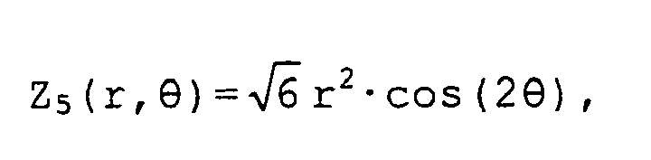

and
- The radial coordinate r in this case denotes the radial coordinate, i.e. the distance from the optical axis, and θ denotes the azimuth angle.
- The Zernike polynomial Z5(r,θ) represented in
Figure 2 is an even function with respect to point reflections on the optical axis. For such a point reflection, which is described by the coordinate transformation
θ → θ + 180° and
r → r
the following applies
- Since it is independent of the azimuth angle θ, the Zernike polynomial Z9(r,θ) represented in
Figure 3 is likewise an even function with respect to point reflections. - The Zernike polynomial Z8(r,θ) represented in
Figure 4 , however, is an odd function with respect to such point reflections, since
- If it is assumed here for the sake of simplicity that the field dependency of a wavefront deformation can be described just by the Zernike polynomial Z5, which is even with respect to point reflections, then it can be seen that such a field dependency is unchanged by an image inversion associated with passing through a pupil plane or intermediate image plane E1, E3, or E2. Similar considerations apply to the rotationally symmetric wavefront deformation represented in
Figure 3 , since this is described by the Zernike polynomial Z9 which is also even. - The situation, however, is different for a wavefront deformation whose field dependency can be described just by an odd Zernike polynomial, for example the Zernike polynomial Z8 represented in
Figure 4 . In this case, the effect of the image inversion at a pupil plane or intermediate image plane E1, E3, or E2 is that the field dependencies are no longer the same before and after such a plane. - If the
perturbation 22 on the lens L2 is now to be compensated for by reprocessing an optically active surface on one of the other optical elements, then the aforementioned different symmetry properties of the field dependencies when the light waves pass through pupil planes or intermediate image planes E1, E2, E3 have wide-ranging consequences. This is because since the field dependencies of the wavefront deformations can generally be described only by a combination of even and odd Zernike polynomials, the field-dependency components assigned to these polynomials are transformed in different ways when passing through pupil planes or intermediate image planes E1, E2, E3. - This means that in the section A2 next to the section A1 containing the
perturbation 22, it is generally not possible to find an optically active surface on optical elements contained therein with which the odd components of the field dependencies can be eliminated by suitable reprocessing. Perturbation compensation on a single optically active surface in this section A2 is successful only for the even components of the field dependency. - In the subsequent section A3, however, it is again possible to compensate substantially for the
perturbation 22 in the section A1 by reprocessing a single optically active surface, since the image inversions caused by the pupil plane E1 and the intermediate image plane E2 balance each other out. - The different corrective potentials of optically active surfaces, according to which of the sections A1 to A4 contains the corresponding surface, has been demonstrated with the aid of simulations. Table 1 gives the residual error remaining as an RMS (root mean square value) and the corrective potential, indicated as a percentage, for suitably reprocessed surfaces Fi in different sections A1 to A4. The simulation is in this case based on the assumption that the
perturbation 22 on the lens L2 can be described by the Zernike polynomial Z13. - It can be seen clearly from the table that only the surfaces F6 and F24, respectively lying in the same section A1 and in the next but one section A3, can substantially reduce the imaging errors due to the
perturbation 22 by suitable reprocessing, and therefore have a large corrective potential. The surfaces F16 and F46 which lie in the sections A2 and A4, respectively, and which would likewise be considered for conventional corrective surface configuration, have only a very small corrective potential compared with these.Table 1: Corrective potential of different correction surfaces REPROCESSED SURFACE SECTION ERROR (RMS) CORRECTIVE POTENTIAL no reprocessing - 1.6 0% F6 A1 0.1 95.7% F16 A2 1.3 15.8% F24 A3 0.2 86.1% F46 A4 1.3 21.7% - In the preceding discussion, it was assumed that there is only one
perturbation 22 whose position is known. However, a wavefront deformation is contributed to in general by a plurality of perturbations, which furthermore cannot be located, or at least not with tolerable outlay. This means that it is not generally possible correct a wavefront deformation by a single reprocessed surface. If one surface in the section A1 and another surface in the section A3 were reprocessed, for example, then generally no contributions to the wavefront deformation which are attributable to perturbations in the section A2 lying in between could therefore be corrected. - It follows from this argument that an effective correction of unknown perturbations can generally be carried out only by reprocessing surfaces in at least two sections which are consecutive, or between which there are an even number of other sections. In the present exemplary embodiment, these could be the section combinations A1 and A2, A2 and A3, A3 and A4, A1 and A4.
- With the measures described above, it is only possible to correct components of a wavefront deformation which vary from field point to field point. A field-independent component (offset) of a wavefront deformation, i.e. one which is common to all the field points, cannot be corrected by local reprocessing of surfaces in the sections A1 to A4, but only by reprocessing of surfaces which lie in or close to one of the pupil planes E1, E3. Since wavefront deformations often have such an offset component as well, not just two but three surfaces will have to be reprocessed in order to be able to at least approximately correct wavefront deformations of the most general type.
Claims (6)
- Projection objective of a microlithographic projection
exposure apparatus, comprising a plurality of optical elements (P, S, L1 to L8, L13, L19) arranged in N ≥ 2 successive sections A1 to AN of the projection objective (10) which are separated from one another by pupil planes (E1, E3) or intermediate image planes (E2),
characterised in that
in order to correct a wavefront deformation, at least two optical elements respectively have an optically active surface locally reprocessed aspherically, a first optical element being arranged in one section Aj, j = 1...N and a second optical element being arranged in another section Ak, k = 1...N, and the absolute value difference |k - j| being an odd number greater than 1. - Projection objective according to Claim 1, characterised
in that a third optical element, which is arranged in or close to a pupil plane (E1, E3), also has an optically active surface locally reprocessed aspherically. - Projection objective according to Claim 1 or 2, characterised in that the local reprocessing is not rotationally symmetric with respect to an optical axis.
- Projection objective according to one of the preceding
claims, characterised in that the reprocessing is carried out by local material erosion. - Projection objective according to Claim 4, characterised
in that the local material erosion amounts to less than 500 nm, preferably less than 200 nm. - Projection objective according to one of the preceding
claims, characterised in that the wavefront deformation is caused by a form error or a refractive index inhomogeneity in one of the optical elements.
Applications Claiming Priority (2)
| Application Number | Priority Date | Filing Date | Title |
|---|---|---|---|
| US57852204P | 2004-06-10 | 2004-06-10 | |
| PCT/EP2005/005930 WO2005121899A1 (en) | 2004-06-10 | 2005-06-02 | Projection objective for a microlithographic projection exposure apparatus |
Publications (2)
| Publication Number | Publication Date |
|---|---|
| EP1754110A1 EP1754110A1 (en) | 2007-02-21 |
| EP1754110B1 true EP1754110B1 (en) | 2008-07-30 |
Family
ID=34970291
Family Applications (1)
| Application Number | Title | Priority Date | Filing Date |
|---|---|---|---|
| EP05751684A Ceased EP1754110B1 (en) | 2004-06-10 | 2005-06-02 | Projection objective for a microlithographic projection exposure apparatus |
Country Status (6)
| Country | Link |
|---|---|
| US (6) | US8064041B2 (en) |
| EP (1) | EP1754110B1 (en) |
| JP (2) | JP5629050B2 (en) |
| KR (2) | KR101500052B1 (en) |
| DE (1) | DE602005008591D1 (en) |
| WO (1) | WO2005121899A1 (en) |
Families Citing this family (8)
| Publication number | Priority date | Publication date | Assignee | Title |
|---|---|---|---|---|
| KR101500052B1 (en) | 2004-06-10 | 2015-03-09 | 칼 짜이스 에스엠티 게엠베하 | Projection objective for a microlithographic projection exposure apparatus |
| EP1746463A2 (en) | 2005-07-01 | 2007-01-24 | Carl Zeiss SMT AG | Method for correcting a lithographic projection objective and projection objective of such a kind |
| JP5174810B2 (en) | 2006-06-16 | 2013-04-03 | カール・ツァイス・エスエムティー・ゲーエムベーハー | Projection objective of microlithography projection exposure apparatus |
| US9715214B2 (en) | 2010-09-24 | 2017-07-25 | The Arizona Board Of Regents On Behalf Of The University Of Arizona | Confocal rainbow volume holographic imaging system |
| WO2013059727A1 (en) * | 2011-10-21 | 2013-04-25 | The Arizona Board Of Regents On Behalf Of The University Of Arizona | Volume holographic imaging system (vhis) endoscope |
| DE102012112773B4 (en) * | 2012-12-20 | 2020-04-30 | Jenoptik Optical Systems Gmbh | Method for producing a wavefront-corrected optical arrangement from at least two optical elements and use of the method |
| JP6360825B2 (en) | 2013-04-03 | 2018-07-18 | オリンパス株式会社 | Imaging optical system, illumination device and observation device |
| DE112015003924T5 (en) * | 2014-10-03 | 2017-05-18 | Olympus Corporation | Microscope device for scanning in the direction of the optical axis |
Family Cites Families (38)
| Publication number | Priority date | Publication date | Assignee | Title |
|---|---|---|---|---|
| FI81898C (en) * | 1988-06-23 | 1990-12-10 | Partek Ab | ANORDNING FOER RULLNING AV ISOLERMATERIALSKIKT. |
| US5117255A (en) | 1990-09-19 | 1992-05-26 | Nikon Corporation | Projection exposure apparatus |
| US5148314A (en) | 1991-06-06 | 1992-09-15 | Chen Chungte W | Optical systems employing refractive and diffractive optical elements to correct for chromatic aberration |
| US5592259A (en) | 1991-08-09 | 1997-01-07 | Nikon Corporation | Photomask, an exposure method and a projection exposure apparatus |
| US5392119A (en) | 1993-07-13 | 1995-02-21 | Litel Instruments | Plate correction of imaging systems |
| JP3341269B2 (en) | 1993-12-22 | 2002-11-05 | 株式会社ニコン | Projection exposure apparatus, exposure method, semiconductor manufacturing method, and projection optical system adjustment method |
| US6333776B1 (en) | 1994-03-29 | 2001-12-25 | Nikon Corporation | Projection exposure apparatus |
| JP3893626B2 (en) | 1995-01-25 | 2007-03-14 | 株式会社ニコン | Projection optical apparatus adjustment method, projection optical apparatus, exposure apparatus, and exposure method |
| US6545746B1 (en) * | 1996-03-04 | 2003-04-08 | Nikon Corporation | Projection exposure apparatus |
| DE69702641T2 (en) | 1996-03-07 | 2001-04-05 | Koninkl Philips Electronics Nv | EXPOSURE SYSTEM AND EXPOSURE DEVICE FOR UV LITHOGRAPHY |
| US6157498A (en) | 1996-06-19 | 2000-12-05 | Nikon Corporation | Dual-imaging optical system |
| DE19639586A1 (en) | 1996-09-26 | 1998-04-02 | Zeiss Carl Fa | Catadioptric microlithography reduction lens |
| JP4192279B2 (en) | 1996-09-27 | 2008-12-10 | 株式会社ニコン | Projection optical system manufacturing method, projection optical system manufactured by the manufacturing method, projection exposure apparatus and method, and semiconductor device manufacturing method |
| JPH1145842A (en) | 1997-07-24 | 1999-02-16 | Nikon Corp | Projection exposure apparatus and exposure method, adjustment method of the exposure apparatus, and circuit device manufacturing method |
| US6522386B1 (en) | 1997-07-24 | 2003-02-18 | Nikon Corporation | Exposure apparatus having projection optical system with aberration correction element |
| JP2000091209A (en) | 1998-09-14 | 2000-03-31 | Nikon Corp | Exposure apparatus manufacturing method, exposure apparatus, and device manufacturing method |
| US6396067B1 (en) | 1998-05-06 | 2002-05-28 | Koninklijke Philips Electronics N.V. | Mirror projection system for a scanning lithographic projection apparatus, and lithographic apparatus comprising such a system |
| DE19827603A1 (en) | 1998-06-20 | 1999-12-23 | Zeiss Carl Fa | Projection light exposure system for microlithography |
| US6867922B1 (en) * | 1999-06-14 | 2005-03-15 | Canon Kabushiki Kaisha | Projection optical system and projection exposure apparatus using the same |
| JP4717974B2 (en) | 1999-07-13 | 2011-07-06 | 株式会社ニコン | Catadioptric optical system and projection exposure apparatus provided with the optical system |
| US6366389B1 (en) | 1999-08-17 | 2002-04-02 | Michael Wraback | High contrast, ultrafast optically-addressed ultraviolet light modulator based upon optical anisotropy |
| JP2001168000A (en) * | 1999-12-03 | 2001-06-22 | Nikon Corp | Method of manufacturing exposure apparatus and method of manufacturing micro device using exposure apparatus manufactured by the method |
| TW538256B (en) | 2000-01-14 | 2003-06-21 | Zeiss Stiftung | Microlithographic reduction projection catadioptric objective |
| JP2002250865A (en) * | 2000-06-14 | 2002-09-06 | Nikon Corp | Projection optical system, exposure apparatus, and manufacturing method thereof |
| JP4245286B2 (en) | 2000-10-23 | 2009-03-25 | 株式会社ニコン | Catadioptric optical system and exposure apparatus provided with the optical system |
| JP2004514943A (en) | 2000-11-28 | 2004-05-20 | カール・ツアイス・エスエムテイ・アーゲー | Catadioptric projection system for 157nm lithography |
| JP4552337B2 (en) | 2000-12-28 | 2010-09-29 | 株式会社ニコン | Projection optical system manufacturing method and exposure apparatus manufacturing method |
| DE10120446C2 (en) * | 2001-04-26 | 2003-04-17 | Zeiss Carl | Projection exposure system and method for compensating imaging errors in a projection exposure system, in particular for micro-lithography |
| US20040246595A1 (en) | 2001-05-15 | 2004-12-09 | Beach Allan David | Optical imaging system with aberration correcting means |
| EP1306698A1 (en) * | 2001-10-26 | 2003-05-02 | Nikon Corporation | Multilayer reflective mirrors for EUV, wavefront-aberration-correction methods for the same, and EUV optical systems comprising the same |
| EP1369608A3 (en) | 2002-05-23 | 2005-06-01 | Nsk Ltd | Linear guide apparatus |
| EP1523692A2 (en) | 2002-07-18 | 2005-04-20 | Carl Zeiss SMT AG | Catadioptric projection objective |
| CN100462844C (en) * | 2002-08-23 | 2009-02-18 | 株式会社尼康 | Projection optical system, lithography method, exposure device and method of using same |
| DE10258715B4 (en) | 2002-12-10 | 2006-12-21 | Carl Zeiss Smt Ag | Method for producing an optical imaging system |
| EP2722703A3 (en) | 2003-05-06 | 2014-07-23 | Nikon Corporation | Projection optical system, and exposure apparatus and exposure method |
| JP2005064310A (en) | 2003-08-18 | 2005-03-10 | Nikon Corp | Optical system aberration adjustment method, optical system, exposure apparatus, and exposure method |
| KR101500052B1 (en) | 2004-06-10 | 2015-03-09 | 칼 짜이스 에스엠티 게엠베하 | Projection objective for a microlithographic projection exposure apparatus |
| EP1746463A2 (en) | 2005-07-01 | 2007-01-24 | Carl Zeiss SMT AG | Method for correcting a lithographic projection objective and projection objective of such a kind |
-
2005
- 2005-06-02 KR KR1020127024577A patent/KR101500052B1/en not_active Expired - Lifetime
- 2005-06-02 EP EP05751684A patent/EP1754110B1/en not_active Ceased
- 2005-06-02 WO PCT/EP2005/005930 patent/WO2005121899A1/en not_active Ceased
- 2005-06-02 KR KR1020067025324A patent/KR101492266B1/en not_active Expired - Lifetime
- 2005-06-02 JP JP2007526253A patent/JP5629050B2/en not_active Expired - Fee Related
- 2005-06-02 DE DE602005008591T patent/DE602005008591D1/en not_active Expired - Lifetime
- 2005-06-02 US US11/570,263 patent/US8064041B2/en active Active
-
2011
- 2011-10-13 US US13/272,440 patent/US8902407B2/en not_active Expired - Lifetime
-
2013
- 2013-06-18 JP JP2013127604A patent/JP5681236B2/en not_active Expired - Fee Related
-
2014
- 2014-10-06 US US14/506,992 patent/US9280058B2/en not_active Expired - Lifetime
-
2016
- 2016-01-28 US US15/008,519 patent/US9588445B2/en not_active Expired - Fee Related
-
2017
- 2017-01-20 US US15/411,015 patent/US9977338B2/en not_active Expired - Fee Related
-
2018
- 2018-04-26 US US15/963,278 patent/US20180373155A1/en not_active Abandoned
Also Published As
| Publication number | Publication date |
|---|---|
| WO2005121899A1 (en) | 2005-12-22 |
| JP5681236B2 (en) | 2015-03-04 |
| US20120033296A1 (en) | 2012-02-09 |
| US9588445B2 (en) | 2017-03-07 |
| US20160282729A1 (en) | 2016-09-29 |
| JP2013228751A (en) | 2013-11-07 |
| JP5629050B2 (en) | 2014-11-19 |
| US9280058B2 (en) | 2016-03-08 |
| KR101500052B1 (en) | 2015-03-09 |
| US20150055109A1 (en) | 2015-02-26 |
| KR101492266B1 (en) | 2015-02-11 |
| DE602005008591D1 (en) | 2008-09-11 |
| KR20120130229A (en) | 2012-11-29 |
| US20180373155A1 (en) | 2018-12-27 |
| KR20070020059A (en) | 2007-02-16 |
| US8064041B2 (en) | 2011-11-22 |
| JP2008502012A (en) | 2008-01-24 |
| EP1754110A1 (en) | 2007-02-21 |
| US20170227853A1 (en) | 2017-08-10 |
| US9977338B2 (en) | 2018-05-22 |
| US20080123069A1 (en) | 2008-05-29 |
| US8902407B2 (en) | 2014-12-02 |
Similar Documents
| Publication | Publication Date | Title |
|---|---|---|
| US9977338B2 (en) | Projection objective for a microlithographic projection exposure apparatus | |
| JP4178862B2 (en) | Reflective projection lens for EUV photolithography | |
| US8659744B2 (en) | Method for correcting a lithography projection objective, and such a projection objective | |
| JP2004525398A (en) | Projection system for EUV lithography | |
| US10018907B2 (en) | Method of operating a microlithographic projection apparatus | |
| KR102881419B1 (en) | Projection optical unit for microlithography and method for manufacturing structured components | |
| US20090213345A1 (en) | Microlithography exposure apparatus using polarized light and microlithography projection system having concave primary and secondary mirrors | |
| JP5913471B2 (en) | Catadioptric projection objective having an inclined deflection mirror, projection exposure apparatus, projection exposure method, and mirror | |
| WO2014012660A2 (en) | Method for operating a microlithographic projection exposure apparatus | |
| SG182908A1 (en) | Illumination system, lithographic apparatus and method | |
| US20100231884A1 (en) | Imaging optical system and related installation and method | |
| EP2761355B1 (en) | Imaging catoptric euv projection optical unit | |
| US20070223119A1 (en) | Reflection-type projection-optical systems, and exposure apparatus comprising same | |
| US9933710B2 (en) | Projection exposure method and projection exposure apparatus | |
| US20070297047A1 (en) | Projection optical system | |
| KR20080011301A (en) | Imaging systems that can be used in imaging systems, in particular microlithographic projection illumination units | |
| US7522260B1 (en) | Method for correcting astigmatism in a microlithography projection exposure apparatus, a projection objective of such a projection exposure apparatus, and a fabrication method for micropatterned components | |
| Ishiyama et al. | High-NA projection lens design for exposure tools |
Legal Events
| Date | Code | Title | Description |
|---|---|---|---|
| PUAI | Public reference made under article 153(3) epc to a published international application that has entered the european phase |
Free format text: ORIGINAL CODE: 0009012 |
|
| 17P | Request for examination filed |
Effective date: 20061130 |
|
| AK | Designated contracting states |
Kind code of ref document: A1 Designated state(s): DE NL |
|
| DAX | Request for extension of the european patent (deleted) | ||
| RBV | Designated contracting states (corrected) |
Designated state(s): DE NL |
|
| GRAP | Despatch of communication of intention to grant a patent |
Free format text: ORIGINAL CODE: EPIDOSNIGR1 |
|
| GRAS | Grant fee paid |
Free format text: ORIGINAL CODE: EPIDOSNIGR3 |
|
| GRAA | (expected) grant |
Free format text: ORIGINAL CODE: 0009210 |
|
| AK | Designated contracting states |
Kind code of ref document: B1 Designated state(s): DE NL |
|
| REF | Corresponds to: |
Ref document number: 602005008591 Country of ref document: DE Date of ref document: 20080911 Kind code of ref document: P |
|
| PLBE | No opposition filed within time limit |
Free format text: ORIGINAL CODE: 0009261 |
|
| STAA | Information on the status of an ep patent application or granted ep patent |
Free format text: STATUS: NO OPPOSITION FILED WITHIN TIME LIMIT |
|
| 26N | No opposition filed |
Effective date: 20090506 |
|
| PGFP | Annual fee paid to national office [announced via postgrant information from national office to epo] |
Ref country code: DE Payment date: 20170621 Year of fee payment: 13 |
|
| PGFP | Annual fee paid to national office [announced via postgrant information from national office to epo] |
Ref country code: NL Payment date: 20170620 Year of fee payment: 13 |
|
| REG | Reference to a national code |
Ref country code: DE Ref legal event code: R119 Ref document number: 602005008591 Country of ref document: DE |
|
| REG | Reference to a national code |
Ref country code: NL Ref legal event code: MM Effective date: 20180701 |
|
| PG25 | Lapsed in a contracting state [announced via postgrant information from national office to epo] |
Ref country code: NL Free format text: LAPSE BECAUSE OF NON-PAYMENT OF DUE FEES Effective date: 20180701 |
|
| PG25 | Lapsed in a contracting state [announced via postgrant information from national office to epo] |
Ref country code: DE Free format text: LAPSE BECAUSE OF NON-PAYMENT OF DUE FEES Effective date: 20190101 |
|
| P01 | Opt-out of the competence of the unified patent court (upc) registered |
Effective date: 20230525 |